ICGOO在线商城 > 集成电路(IC) > 数据采集 - ADCs/DAC - 专用型 > AD7891ASZ-2
 Datasheet下载
- 型号: AD7891ASZ-2
- 制造商: Analog
- 库位|库存: xxxx|xxxx
- 要求:
| 数量阶梯 | 香港交货 | 国内含税 |
| +xxxx | $xxxx | ¥xxxx |
查看当月历史价格
查看今年历史价格
AD7891ASZ-2产品简介:
ICGOO电子元器件商城为您提供AD7891ASZ-2由Analog设计生产,在icgoo商城现货销售,并且可以通过原厂、代理商等渠道进行代购。 AD7891ASZ-2价格参考。AnalogAD7891ASZ-2封装/规格:数据采集 - ADCs/DAC - 专用型, 数据采集系统(DAS) 12 b 500k 串行,并联 44-MQFP(10x10)。您可以下载AD7891ASZ-2参考资料、Datasheet数据手册功能说明书,资料中有AD7891ASZ-2 详细功能的应用电路图电压和使用方法及教程。
AD7891ASZ-2是Analog Devices Inc.(ADI公司)生产的一款专用型数据采集ADC(模数转换器)。它属于AD789x系列,是一款高精度、低功耗的12位逐次逼近寄存器(SAR)ADC。以下是其主要应用场景:

 1. 工业自动化与控制
AD7891ASZ-2广泛应用于工业自动化系统中,特别是在需要精确测量和控制的场合。例如,在温度、压力、流量等传感器信号的采集过程中,该ADC可以提供高精度的数据转换,确保控制系统能够准确获取环境参数,从而实现高效的闭环控制。

 2. 电力监控与能源管理
在电力监控系统中,AD7891ASZ-2可用于电压、电流等电参数的实时监测。它的高精度和低功耗特性使得它非常适合用于智能电网、电表等设备中,帮助实现精确的能量计量和管理。

 3. 医疗设备
该ADC也适用于医疗设备中的信号采集,如心电图(ECG)、血压计等。这些设备要求ADC具备高分辨率和低噪声特性,以确保采集到的生理信号准确无误。AD7891ASZ-2的低功耗和小尺寸设计使其非常适合便携式医疗设备。

 4. 汽车电子
在汽车电子领域,AD7891ASZ-2可用于各种传感器信号的采集,如发动机温度、车速、油压等。它能够在恶劣的汽车环境中稳定工作,并提供可靠的数据转换,支持车辆的智能化管理和安全控制。

 5. 测试与测量仪器
AD7891ASZ-2还常用于各种测试与测量仪器中,如示波器、万用表等。这些仪器需要高精度的ADC来捕捉微弱的电信号,而AD7891ASZ-2的性能正好满足这一需求,确保测量结果的准确性。

 6. 消费电子产品
在一些高端消费电子产品中,如智能家居设备、音频处理设备等,AD7891ASZ-2也可以发挥重要作用。它的小尺寸和低功耗特性使其适合集成到小型化、便携式的消费电子产品中,同时保证了产品的性能和用户体验。

总之,AD7891ASZ-2凭借其高精度、低功耗、小尺寸等特点,广泛应用于多个领域,尤其适合对数据采集精度要求较高的应用场景。
| 参数 | 数值 |
| 产品目录 | 集成电路 (IC)半导体 |
| 描述 | IC DAS 12BIT 8CH 44-MQFP模数转换器 - ADC Bipolar Inpt SGL-Sup Parallel 8CH 12B |
| 产品分类 | |
| 品牌 | Analog Devices Inc |
| 产品手册 | |
| 产品图片 |
|
| rohs | 符合RoHS无铅 / 符合限制有害物质指令(RoHS)规范要求 |
| 产品系列 | 数据转换器IC,模数转换器 - ADC,Analog Devices AD7891ASZ-2- |
| 数据手册 | |
| 产品型号 | AD7891ASZ-2 |
| 产品种类 | 模数转换器 - ADC |
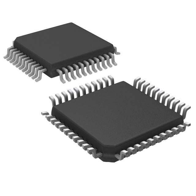
| 供应商器件封装 | 44-MQFP(10x10) |
| 信噪比 | 70 dB |
| 其它名称 | AD7891ASZ2 |
| 分辨率 | 12 bit |
| 分辨率(位) | 12 b |
| 包装 | 托盘 |
| 商标 | Analog Devices |
| 安装类型 | 表面贴装 |
| 安装风格 | SMD/SMT |
| 封装 | Tray |
| 封装/外壳 | 44-QFP |
| 封装/箱体 | QFP-44 |
| 工作温度 | -40°C ~ 85°C |
| 工作电源电压 | 5 V |
| 工厂包装数量 | 96 |
| 接口类型 | Parallel, Serial (5-Wire) |
| 数据接口 | 串行,并联 |
| 最大功率耗散 | 100 mW |
| 最大工作温度 | + 105 C |
| 最小工作温度 | - 40 C |
| 标准包装 | 1 |
| 电压-电源 | 5V |
| 电压参考 | Internal, External |
| 电压源 | 单电源 |
| 类型 | 数据采集系统(DAS) |
| 系列 | AD7891 |
| 结构 | SAR |
| 转换器数量 | 1 |
| 转换速率 | 500 kS/s |
| 输入类型 | Single-Ended |
| 通道数量 | 8 Channel |
| 采样率(每秒) | 500k |


PDF Datasheet 数据手册内容提取
a LC2MOS 8-Channel, 12-Bit High Speed Data Acquisition System AD7891 FEATURES FUNCTIONAL BLOCK DIAGRAM Fast 12-Bit ADC with 1.6(cid:1)s Conversion Time REF OUT/ 8 Single-Ended Analog Input Channels VDD VDD REF IN REF GND Overvoltage Protection on Each Channel Selection of Input Ranges: VIN1A (cid:2)0 5to V +, 2(cid:2).51 0V ,V 0 f otor A+5D 7V8, 9(cid:2)12-1.5 V for AD7891-2 VVVIIINNN122BAB AD7891 REFE2.R5EVNCE STANDBY Parallel and Serial Interface VIN3A On-Chip Track/Hold Amplifier VIN3B On-Chip Reference VVIINN44AB MU 1A2-DBCIT Single-Supply, Low Power Operation (100mW Max) VIN5A X Power-Down Mode (75(cid:1)W Typ) VVIINN56BA TRACK/HOLD ADaPtPaL IACcAqTuIiOsiNtiSon Systems VVVIIINNN677BAB ADDEDCROEDSES DCLIAONTNEATSR/OL Motor Control VIN8A Mobile Communication Base Stations VIN8B CLOCK Instrumentation CONTROL LOGIC WRCSRDEOCCONVSTMODE AGNDAGNDDGND GENERAL DESCRIPTION PRODUCT HIGHLIGHTS The AD7891 is an 8-channel, 12-bit data acquisition system 1. The AD7891 is a complete monolithic 12-bit data acquisition with a choice of either parallel or serial interface structure. The system that combines an 8-channel multiplexer, 12-bit ADC, part contains an input multiplexer, an on-chip track/hold ampli- 2.5V reference, and track/hold amplifier on a single chip. fier, a high speed 12-bit ADC, a 2.5V reference, and a high 2. The AD7891-2 features a conversion time of 1.6ms and an speed interface. The part operates from a single 5 V supply and acquisition time of 0.4ms. This allows a sample rate of accepts a variety of analog input ranges across two models, the 500kSPS when sampling one channel and 62.5kSPS when AD7891-1 (±5V and ±10V) and the AD7891-2 (0V to +2.5 V, channel hopping. These sample rates can be achieved using 0V to +5V, and ±2.5V). either a software or hardware convert start. The AD7891-1 The AD7891 provides the option of either a parallel or serial has an acquisition time of 0.6 ms when using a hardware interface structure determined by the MODE pin. The part convert start and an acquisition time of 0.7ms when using a has standard control inputs and fast data access times for both software convert start. These acquisition times allow sample the serial and parallel interfaces, ensuring easy interfacing to rates of 454.5 kSPS and 435 kSPS, respectively, for hardware modern microprocessors, microcontrollers, and digital signal and software convert start. processors. 3. Each channel on the AD7891 has overvoltage protection. This In addition to the traditional dc accuracy specifications, such as means an overvoltage on an unselected channel does not affect linearity, full-scale and offset errors, the part is also specified for the conversion on a selected channel. The AD7891-1 can dynamic performance parameters, including harmonic distortion withstand overvoltages of ±17V. and signal-to-noise ratio. Power dissipation in normal mode is 82mW typical; in the standby mode, this is reduced to 75mW typ. The part is available in a 44-terminal MQFP and a 44-lead PLCC. REV.D Information furnished by Analog Devices is believed to be accurate and reliable. However, no responsibility is assumed by Analog Devices for its use, nor for any infringements of patents or other rights of third parties that may result from its use. No license is granted by implication or otherwise One Technology Way, P.O. Box 9106, Norwood, MA 02062-9106, U.S.A. under any patent or patent rights of Analog Devices. Trademarks and Tel: 781/329-4700 www.analog.com registered trademarks are the property of their respective owners. Fax: 781/326-8703 © 2004 Analog Devices, Inc. All rights reserved.
AD7891–SPECIFICATIONS (V = 5V (cid:2) 5%, AGND = DGND = 0V, REF IN = 2.5V. All specifications T to T , DD MIN MAX unless otherwise noted.) Parameter A Version1 B Version Y Version Unit Test Conditions/Comments DYNAMIC PERFORMANCE2 Sample Rate = 454.5 kSPS3 (AD7891-1), 500 kSPS3 (AD7891-2). Any channel. Signal-to-(Noise + Distortion) Ratio4 @ 25∞C 70 70 70 dB min T to T 70 70 70 dB min MIN MAX Total Harmonic Distortion4 –78 –78 –78 dB max Peak Harmonic or Spurious Noise4 –80 –80 –80 dB max Intermodulation Distortion4 fa = 9kHz, fb = 9.5kHz. Second-Order Terms –80 –80 –80 dB typ Third-Order Terms –80 –80 –80 dB typ Channel-to-Channel Isolation4 –80 –80 –80 dB max DC ACCURACY Any channel. Resolution 12 12 12 Bits Minimum Resolution for which No Missing Codes Are Guaranteed 12 12 12 Bits Relative Accuracy4 ±1 ±0.75 ±1 LSB max Differential Nonlinearity4 ±1 ±1 ±1 LSB max Positive Full-Scale Error4 ±3 ±3 ±3 LSB max Positive Full-Scale Error Match4, 5 0.6 0.6 0.6 LSB typ 1.5 LSB max. Unipolar Offset Error ±4 ±4 ±4 LSB max Input ranges of 0 V to 2.5V, 0 V to 5V. Unipolar Offset Error Match5 0.1 0.1 0.1 LSB typ 1 LSB max. Negative Full-Scale Error4 ±3 ±3 ±3 LSB max Input ranges of ±2.5V, ±5V, ±10V. Negative Full-Scale Error Match4, 5 0.6 0.6 0.6 LSB typ 1.5 LSB max. Bipolar Zero Error ±4 ±4 ±4 LSB max Input ranges of ±2.5V, ±5V, ±10V. Bipolar Zero Error Match5 0.2 0.2 0.2 LSB typ 1.5 LSB max. ANALOG INPUTS AD7891-1 Input Voltage Range ±5 ±5 ±5 V Input applied to both VINXA and VINXB. ±10 ±10 ±10 V Input applied to VINXA, VINXB = AGND. AD7891-1 VINXA Input Resistance 7.5 7.5 7.5 kW min Input range of ±5V. AD7891-1 VINXA Input Resistance 15 15 15 kW min Input range of ±10V. AD7891-2 Input Voltage Range 0 to 2.5 0 to 2.5 0 to 2.5 V Input applied to both V and V . INXA INXB 0 to 5 0 to 5 0 to 5 V Input applied to V , V = AGND. INXA INXB ±2.5 ±2.5 ±2.5 V Input applied to VINXA, VINXB = REF IN6. AD7891-2 VINXA Input Resistance 1.5 1.5 1.5 kW min Input ranges of ±2.5V and 0 V to 5V. AD7891-2 VINXA Input Current ±50 ±50 ±50 nA max Input range of 0 V to 2.5V. REFERENCE INPUT/OUTPUT REF IN Input Voltage Range 2.375/2.625 2.375/2.625 2.375/2.625 V min/V max 2.5 V ± 5%. Input Impedance 1.6 1.6 1.6 kW min Resistor connected to internal reference node. Input Capacitance5 10 10 10 pF max REF OUT Output Voltage 2.5 2.5 2.5 Vnom REF OUT Error @ 25∞C ±10 ±10 ±10 mV max TMIN to TMAX ±20 ±20 ±20 mV max REF OUT Temperature Coefficient 25 25 25 ppm/∞C typ REF OUT Output Impedance 5 5 5 kW nom See REF IN input impedance. LOGIC INPUTS Input High Voltage, VINH 2.4 2.4 2.4 V min VDD = 5 V ± 5%. Input Low Voltage, VINL 0.8 0.8 0.8 V max VDD = 5 V ± 5%. Input Current, IINH ±10 ±10 ±10 mA max Input Capacitance5 C 10 10 10 pF max IN –2– REV. D
AD7891 Parameter A Version1 B Version Y Version Unit Test Conditions/Comments LOGIC OUTPUTS Output High Voltage, VOH 4.0 4.0 4.0 V min ISOURCE = 200mA. Output Low Voltage, V 0.4 0.4 0.4 V max I = 1.6mA. OL SINK DB11to DB0 Floating-State Leakage Current ±10 ±10 ±10 mA max Floating-State Capacitance5 15 15 15 pF max Output Coding Straight (Natural) Binary Data format bit of control register = 0. Twos Complement Data format bit of control register = 1. CONVERSION RATE Conversion Time 1.6 1.6 1.6 ms max Track/Hold Acquisition Time 0.6 0.6 0.6 ms max AD7891-1 hardware conversion. 0.7 0.7 0.7 ms max AD7891-1 software conversion. 0.4 0.4 0.4 ms max AD7891-2. POWER REQUIREMENTS VDD 5 5 5 V nom ±5% for specified performance. I DD Normal Mode 20 20 21 mA max Standby Mode 80 80 80 mA max Logic inputs = 0 V or VDD. Power Dissipation V = 5 V. DD Normal Mode 100 100 105 mW max Typically 82mW. Standby Mode 400 400 400 mW max Typically 75 mW. NOTES 1Temperature ranges for the A and B Versions: –40∞C to +85∞C. Temperature range for the Y Version: –55∞C to +105∞C. 2The AD7891-1’s dynamic performance (THD and SNR) and the AD7891-2’s THD are measured with an input frequency of 10kHz. The AD7891-2’s SNR is evaluated with an input frequency of 100kHz. 3This throughput rate can only be achieved when the part is operated in the parallel interface mode. Maximum achievable throughput rate in the serial interface mode is 357kSPS. 4See the Terminology section. 5Sample tested during initial release and after any redesign or process change that may affect this parameter. 6REF IN must be buffered before being applied to V . INXB Specifications subject to change without notice. ABSOLUTE MAXIMUM RATINGS* Junction Temperature . . . . . . . . . . . . . . . . . . . . . . . . . . 150∞C (TA = 25∞C, unless otherwise noted) MQFP Package, Power Dissipation . . . . . . . . . . . . . . 450 mW VDD to AGND . . . . . . . . . . . . . . . . . . . . . . . . . –0.3 V to +7 V qJA Thermal Impedance . . . . . . . . . . . . . . . . . . . . . . 95∞C/W V to DGND . . . . . . . . . . . . . . . . . . . . . . . . . –0.3 V to +7V Lead Temperature, Soldering DD Analog Input Voltage to AGND Vapor Phase (60 sec) . . . . . . . . . . . . . . . . . . . . . . . . 215∞C AD7891-1 . . . . . . . . . . . . . . . . . . . . . . . . . . . . . . . . . ±17V Infrared (15 sec) . . . . . . . . . . . . . . . . . . . . . . . . . . . 220∞C AD7891-2 . . . . . . . . . . . . . . . . . . . . . . . . . . . . –5 V, +10V PLCC Package, Power Dissipation . . . . . . . . . . . . . . 500 mW Reference Input Voltage to AGND . . . . –0.3 V to VDD + 0.3V qJA Thermal Impedance . . . . . . . . . . . . . . . . . . . . . . 55∞C/W Digital Input Voltage to DGND . . . . . . –0.3 V to V + 0.3 V Lead Temperature, Soldering DD Digital Output Voltage to DGND . . . . . –0.3 V to VDD + 0.3 V Vapor Phase (60 sec) . . . . . . . . . . . . . . . . . . . . . . . . 215∞C Operating Temperature Range Infrared (15 sec) . . . . . . . . . . . . . . . . . . . . . . . . . . . 220∞C Commercial (A, B Versions) . . . . . . . . . . . –40∞C to +85∞C *Stresses above those listed under Absolute Maximum Ratings may cause perma- Automotive (Y Version) . . . . . . . . . . . . . . –55∞C to +105∞C nent damage to the device. This is a stress rating only; functional operation of the Storage Temperature Range . . . . . . . . . . . . –65∞C to +150∞C device at these or any other conditions above those listed in the operational sections of this specification is not implied. Exposure to absolute maximum rating conditions for extended periods may affect device reliability. CAUTION ESD (electrostatic discharge) sensitive device. Electrostatic charges as high as 4000V readily accumulate on the human body and test equipment and can discharge without detection. Although the AD7891 features proprietary ESD protection circuitry, permanent damage may occur on devices subjected to high energy electrostatic discharges. Therefore, proper ESD precautions are recommended to avoid performance degradation or loss of functionality. REV. D –3–
AD7891 TIMING CHARACTERISTICS1, 2 Parameter A, B, Y Versions Unit Test Conditions/Comments tCONV 1.6 ms max Conversion Time Parallel Interface t 0 ns min CS to RD/WR Setup Time 1 t 35 ns min Write Pulse Width 2 t 25 ns min Data Valid to Write Setup Time 3 t 5 ns min Data Valid to Write Hold Time 4 t 0 ns min CS to RD/WR Hold Time 5 t 35 ns min CONVST Pulse Width 6 t 55 ns min EOC Pulse Width 7 t 35 ns min Read Pulse Width 8 t 3 25 ns min Data Access Time after Falling Edge of RD 9 t 4 5 ns min Bus Relinquish Time after Rising Edge of RD 10 30 ns max Serial Interface t 30 ns min RFS Low to SCLK Falling Edge Setup Time 11 t 3 20 ns max RFS Low to Data Valid Delay 12 t 25 ns min SCLK High Pulse Width 13 t 25 ns min SCLK Low Pulse Width 14 t 3 5 ns min SCLK Rising Edge to Data Valid Hold Time 15 t 3 15 ns max SCLK Rising Edge to Data Valid Delay 16 t 20 ns min RFS to SCLK Falling Edge Hold Time 17 t 4 0 ns min Bus Relinquish Time after Rising Edge of RFS 18 30 ns max t 4 0 ns min Bus Relinquish Time after Rising Edge of SCLK 18A 30 ns max t 20 ns min TFS Low to SCLK Falling Edge Setup Time 19 t 15 ns min Data Valid to SCLK Falling Edge Setup Time 20 t 10 ns min Data Valid to SCLK Falling Edge Hold Time 21 t 30 ns min TFS Low to SCLK Falling Edge Hold Time 22 NOTES 1Sample tested during initial release and after any redesign or process change that may affect this parameter. All input signals are measured with tr = tf = 1 ns (10% to 90% of 5V) and timed from a voltage level of 1.6V. 2See Figures 2, 3, and 4. 3Measured with the load circuit of Figure 1 and defined as the time required for an output to cross 0.8V or 2.4V. 4These times are derived from the measured time taken by the data outputs to change 0.5V when loaded with the circuit of Figure 1. The measured number is then extrapolated back to remove the effects of charging or discharging the 50 pF capacitor. This means that the times quoted in the timing characteristics are the true bus relinquish times of the part and as such are independent of external bus loading capacitances. Specifications subject to change without notice. 1.6mA TO OUTPUT 1.6V PIN 50pF 200(cid:1)A Figure 1.Load Circuit for Access Time and Bus Relinquish Time –4– REV. D
AD7891 ORDERING GUIDE Relative Temperature Model Input Range Sample Rate Accuracy Range Package Option1 AD7891ACHIPS-1 DIE AD7891ACHIPS-2 DIE AD7891AS-1 ±5 V or ±10 V 454 kSPS ±1 LSB –40∞C to +85∞C S-44 AD7891ASZ-12 ±5 V or ±10 V 454 kSPS ±1 LSB –40∞C to +85∞C S-44 AD7891AP-1 ±5 V or ±10 V 454 kSPS ±1 LSB –40∞C to +85∞C P-44A AD7891AP-1REEL ±5 V or ±10 V 454 kSPS ±1 LSB –40∞C to +85∞C P-44A AD7891BS-1 ±5 V or ±10 V 454 kSPS ±0.75 LSB –40∞C to +85∞C S-44 AD7891BP-1 ±5 V or ±10 V 454 kSPS ±0.75 LSB –40∞C to +85∞C P-44A AD7891BP-1REEL ±5 V or ±10 V 454 kSPS ±0.75 LSB –40∞C to +85∞C P-44A AD7891YS-1 ±5 V or ±10 V 454 kSPS ±1 LSB –55∞C to +105∞C S-44 AD7891YS-1REEL ±5 V or ±10 V 454 kSPS ±1 LSB –55∞C to +105∞C S-44 AD7891YP-1 ±5 V or ±10 V 454 kSPS ±1 LSB –55∞C to +105∞C P-44A AD7891YP-1REEL ±5 V or ±10 V 454 kSPS ±1 LSB –55∞C to +105∞C P-44A AD7891AS-2 0 V to +5 V, 0 V to +2.5 V, ±2.5 V 500 kSPS ±1 LSB –40∞C to +85∞C S-44 AD7891ASZ-22 0 V to +5 V, 0 V to +2.5 V, ±2.5 V 500 kSPS ±1 LSB –40∞C to +85∞C S-44 AD7891AP-2 0 V to +5 V, 0 V to +2.5 V, ±2.5 V 500 kSPS ±1 LSB –40∞C to +85∞C P-44A AD7891AP-2REEL 0 V to +5 V, 0 V to +2.5 V, ±2.5 V 500 kSPS ±1 LSB –40∞C to +85∞C P-44A AD7891BS-2 0 V to +5 V, 0 V to +2.5 V, ±2.5 V 500 kSPS ±0.75 LSB –40∞C to +85∞C S-44 AD7891BP-2 0 V to +5 V, 0 V to +2.5 V, ±2.5 V 500 kSPS ±0.75 LSB –40∞C to +85∞C P-44A AD7891BP-2REEL 0 V to +5 V, 0 V to +2.5 V, ±2.5 V 500 kSPS ±0.75 LSB –40∞C to +85∞C P-44A AD7891YS-2 0 V to +5 V, 0 V to +2.5 V, ±2.5 V 500 kSPS ±1 LSB –55∞C to +105∞C S-44 AD7891YS-2REEL 0 V to +5 V, 0 V to +2.5 V, ±2.5 V 500 kSPS ±1 LSB –55∞C to +105∞C S-44 EVAL-AD7891-1CB Evaluation Board EVAL-AD7891-2CB Evaluation Board NOTES 1S = Plastic Quad Flatpack (MQFP); P = Plastic Leaded Chip Carrier (PLCC). 2Z = Pb-free part. PIN CONFIGURATIONS PLCC MQFP Y Y B B D D N A B A B A B A B A B N A B A B A B A B A B STAVIN1VIN1VIN2VIN2VIN3VIN3VIN4VIN4VIN5VIN5 STAVIN1VIN1VIN2VIN2VIN3VIN3VIN4VIN4VIN5VIN5 6 5 4 3 2 1 44 43 42 41 40 44 43 42 41 40 39 38 37 36 35 34 REF GNNDC 78 PIDINE N1TIFIER 3398 VVIINN66AB REF GNNDC 12 PIDINE N1TIFIER 3332 VVIINN66AB REF OUT/REF IN 9 37 VIN7A REF OUT/REF IN 3 31 VIN7A VDD 10 36 VIN7B VDD 4 30 VIN7B AGND 11 AD7891 35 VIN8A AGND 5 AD7891 29 VIN8A MODE 12 TOP VIEW 34 VIN8B MODE 6 TOP VIEW 28 VIN8B DB11/TEST 13 (Not to Scale) 33 AGND DB11/TEST 7 (Not to Scale) 27 AGND DB10/TEST 14 32 EOC DB10/TEST 8 26 EOC DB9/TFS 15 31 NC DB9/TFS 9 25 NC DB8/RFS 16 30 CONVST DB8/RFS 10 24 CONVST DB7/DATA IN 17 29 CS DB7/DATA IN 11 23 CS 18 19 20 21 22 23 24 25 26 27 28 12 13 14 15 16 17 18 19 20 21 22 NC = NO CONNECT DB6/SCLKVDDDGND A2/DATA OUTDB4/A1 DB3/A0DB2/SWCON DB1/SWSTBYDB0/FORMAT WRRD NC = NO CONNECT DB6/SCLKVDDDGNDA2/DATA OUT DB4/A1DB3/A0 DB2/SWCONDB1/SWSTBY DB0/FORMAT WRRD B5/ B5/ D D REV. D –5–
AD7891 PIN FUNCTION DESCRIPTIONS PLCC MQFP Pin No. Pin No. Mnemonic Description 1–5 28–43 V , V Analog Input Channels. The AD7891 contains eight pairs of analog input channels. Each INXA INXB 34–44 channel contains two input pins to allow a number of different input ranges to be used with the AD7891. There are two possible input voltage ranges on the AD7891-1. The ±5V input range is selected by connecting the input voltage to both VINXA and VINXB, while the ±10V input range is selected by applying the input voltage to VINXA and con- necting V to AGND. The AD7891-2 has three possible input ranges. The 0V to INXB 2.5V input range is selected by connecting the analog input voltage to both V and V ; the INXA INXB 0V to 5V input range is selected by applying the input voltage to V and connecting INXA VINXB to AGND while the ±2.5V input range is selected by connecting the analog input voltage to V and connecting V to REFIN (provided this REF IN voltage comes INXA INXB from a low impedance source). The channel to be converted is selected by the A2, A1, and A0 bits of the control register. In the parallel interface mode, these bits are available as three data input lines (DB3 to DB5) in a parallel write operation. While in the serial inter- face mode, these three bits are accessed via the DATA IN line in a serial write operation. The multiplexer has guaranteed break-before-make operation. 10, 19 4, 13 VDD Positive Supply Voltage, 5V ± 5%. 11, 33 5, 27 AGND Analog Ground. Ground reference for track/hold, comparator, and DAC. 20 14 DGND Digital Ground. Ground reference for digital circuitry. 6 44 STANDBY Standby Mode Input. TTL compatible input used to put the device into the power save or standby mode. The STANDBY input is high for normal operation and low for standby operation. 9 3 REF OUT/REFIN Voltage Reference Output/Input. The part can either be used with its own internal refer- ence or with an external reference source. The on-chip 2.5V reference voltage is pro- vided at this pin. When using this internal reference as the reference source for the part, REFOUT should be decoupled to REFGND with a 0.1mF disc ceramic capaci- tor. The output impedance of the reference source is typically 2kW. When using an external reference source as the reference voltage for the part, the reference source should be connected to this pin. This overdrives the internal reference and provides the reference source for the part. The reference pin is buffered on-chip but must be able to sink or source current through this 2kW resistor to the output of the on-chip reference. The nominal reference voltage for correct operation of the AD7891 is 2.5V. 7 1 REF GND Reference Ground. Ground reference for the part’s on-chip reference buffer. The REF OUT pin of the part should be decoupled with a 0.1mF capacitor to this REF GND pin. If the AD7891 is used with an external reference, the external reference should also be decoupled to this pin. The REFGND pin should be connected to the AGND pin or the system’s AGND plane. 30 24 CONVST Convert Start. Edge-triggered logic input. A low-to-high transition on this input puts the track/hold into hold and initiates conversion. When changing channels on the part, sufficient time should be given for multiplexer settling and track/hold acquisition between the channel change and the rising edge of CONVST. 32 26 EOC End-of-Conversion. Active low logic output indicating converter status. The end of con- version is signified by a low-going pulse on this line. The duration of this EOC pulse is nominally 80ns. 12 6 MODE Interface Mode. Control input that determines the interface mode for the part. With this pin at a logic low, the AD7891 is in its serial interface mode; with this pin at a logic high, the device is in its parallel interface mode. –6– REV. D
AD7891 PARALLEL INTERFACE MODE FUNCTIONS PLCC Pin No. MQFP Pin No. Mnemonic Description 8, 31 2, 25 NC No Connect. The two NC pins on the device can be left unconnected. If they are to be connected to a voltage, it should be to ground potential. To ensure correct operation of the AD7891, neither of the NC pins should be connected to a logic high potential. 29 23 CS Chip Select Input. Active low logic input that is used in conjunction with to enable the data outputs and with WR to allow input data to be written to the part. 28 22 RD Read Input. Active low logic input that is used in conjunction with CS low to enable the data outputs. 27 21 WR Write Input. Active low logic input used in conjunction with CS to latch the mul- tiplexer address and software control information. The rising edge of this input also initiates an internal pulse. When using the software start facility, this pulse delays the point at which the track/hold goes into hold and conversion is initiated. This allows the multiplexer to settle and the acquisition time of the track/hold to elapse when a channel address is changed. If the SWCON bit of the control regis- ter is set to 1, when this pulse times out, the track/hold then goes into hold and conversion is initiated. If the SWCON bit of the control register is set to 0, the track/hold and conversion sequence are unaffected by WR operation. Data I/O Lines There are 12 data input/output lines on the AD7891. When the part is configured for parallel mode (MODE = 1), the output data from the part is provided at these 12 pins during a read operation. For a write operation in parallel mode, these lines provide access to the part’s control register. Parallel Read Operation During a parallel read operation, the 12 lines become the 12 data bits containing the conversion result from the AD7891. These data bits are labelled Data Bit 0 (LSB) to Data Bit 11 (MSB). They are three-state, TTL compatible outputs. Output data coding is twos complement when the data FORMAT bit of the control register is 1, and straight binary when the data FORMAT bit of the control register is 0. PLCC Pin No. MQFP Pin No. Mnemonic Description 13 to 18, 7 to 12, DB0 to DB11 Data Bit 0 (LSB) to Data Bit 11 (MSB). Three-state TTL compatible 21 to 26 15 to 20 outputs that are controlled by the CS and RD inputs. Parallel Write Operation During a parallel write operation, the following functions can be written to the control register via the 12 data input/output pins. PLCC Pin No. MQFP Pin No. Mnemonic Description 23 17 A0 Address Input. The status of this input during a parallel write operation is latched to the A0 bit of the control register (see Control Register section). 22 16 A1 Address Input. The status of this input during a parallel write operation is latched to the A1 bit of the control register (see Control Register section). 21 15 A2 Address Input. The status of this input during a parallel write operation is latched to the A2 bit of the control register (see Control Register section). 24 18 SWCON Software Conversion Start. The status of this input during a parallel write operation is latched to the SWCONV bit of the control register (see Control Register section). 25 19 SWSTBY Software Standby Control. The status of this input during a parallel write operation is latched to the SWSTBY bit of the control register (see Control Register section). 26 20 FORMAT Data Format Selection. The status of this input during a parallel write operation is latched to the FORMAT bit of the control register (see Control Register section). REV. D –7–
AD7891 SERIAL INTERFACE MODE FUNCTIONS When the part is configured for serial mode (MODE = 0), five of the 12 data input/output lines provide serial interface functions. These functions are outlined below. PLCC Pin No. MQFP Pin No. Mnemonic Description 18 12 SCLK Serial Clock Input. This is an externally applied serial clock that is used to load serial data to the control register and to access data from the output register. 15 9 TFS Transmit Frame Synchronization Pulse. Active low logic input with serial data expected after the falling edge of this signal. 16 10 RFS Receive Frame Synchronization Pulse. This is an active low logic input with RFS provided externally as a strobe or framing pulse to access serial data from the output register. For applications that require that data be transmitted and received at the same time, RFS and TFS should be connected together. 21 15 DATA OUT Serial Data Output. Sixteen bits of serial data are provided with the data FORMAT bit and the three address bits of the control register preceding the 12 bits of conversion data. Serial data is valid on the falling edge of SCLK for 16 edges after RFS goes low. Output conversion data coding is twos complement when the FORMAT bit of the control register is 1 and straight binary when the FORMAT bit of the control register is 0. 17 11 DATA IN Serial Data Input. Serial data to be loaded to the control register is provided at this input. The first six bits of serial data are loaded to the control register on the first six falling edges of SCLK after TFS goes low. Serial data on subsequent SCLK edges is ignored while TFS remains low. 13, 14 7, 8 TEST Test Pin. When the device is configured for serial mode of operation, two of the pins which had been data inputs become test inputs. To ensure correct operation of the device, both TEST inputs should be tied to a logic low potential. CONTROL REGISTER The control register for the AD7891 contains six bits of information as described below. These six bits can be written to the control register either in a parallel mode write operation or via a serial mode write operation. The default (power-on) condition of all bits in the control register is 0. Six serial clock pulses must be provided to the part in order to write data to the control register. If TFS returns high before six serial clock cycles, no data transfer takes place to the control register and the write cycle has to be restarted to write data to the control register. However, if the SWCONV bit of the register was previously set to a Logic 1 and TFS is brought high before six serial clock cycles, another conversion is initiated. LSB(DB0) A2 A1 A0 SWCONV SWSTBY FORMAT A2 Address Input. This input is the most significant address input for multiplexer channel selection. A1 Address Input. This is the second most significant address input for multiplexer channel selection. A0 Address Input. Least significant address input for multiplexer channel selection. When the address is written to the control register, an internal pulse is initiated to allow for the multiplexer settling time and track/hold acquisi- tion time before the track/hold goes into hold and conversion is initiated. When the internal pulse times out, the track/hold goes into hold and conversion is initiated. The selected channel is given by the formula A2¥4+ A1¥2+ A0 +1 SWCONV Conversion Start. Writing a 1 to this bit initiates a conversion in a similar manner to the CONVST input. Con- tinuous conversion starts do not take place when there is a 1 in this location. The internal pulse and the conver- sion process are initiated when a 1 is written to this bit. With a 1 in this bit, the hardware conversion start, i.e., the CONVST input, is disabled. Writing a 0 to this bit enables the hardware CONVST input. SWSTBY Standby Mode Input. Writing a 1 to this bit places the device in its standby or power-down mode. Writing a 0 to this bit places the device in its normal operating mode. FORMAT Data Format. Writing a 0 to this bit sets the conversion data output format to straight (natural) binary. This data format is generally used for unipolar input ranges. Writing a 1 to this bit sets the conversion data output format to twos complement. This output data format is generally used for bipolar input ranges. –8– REV. D
AD7891 TERMINOLOGY Channel-to-Channel Isolation Signal-to-(Noise + Distortion) Ratio Channel-to-channel isolation is a measure of the level of This is the measured ratio of signal to (noise + distortion) at the crosstalk between channels. It is measured by applying a full- output of the ADC. The signal is the rms amplitude of the scale 20kHz (AD7891-1) or 100 kHz (AD7891-2) sine wave fundamental. Noise is the rms sum of all nonfundamental signal to one input channel and determining how much that signals up to half the sampling frequency (f /2), excluding dc. signal is attenuated in each of the other channels. The figure S The ratio is dependent upon the number of quantization levels given is the worst case across all eight channels. in the digitization process; the more levels, the smaller the quan- Relative Accuracy tization noise. The theoretical signal-to-(noise +distortion) ratio Relative accuracy or endpoint nonlinearity is the maximum for an ideal N-bit converter with a sine wave input is given by deviation from a straight line passing through the endpoints of Signal-to-(Noise + Distortion) = (6.02N + 1.76) dB the ADC transfer function. Therefore, for a 12-bit converter, this is 74dB. Differential Nonlinearity This is the difference between the measured and the ideal 1LSB Total Harmonic Distortion (THD) change between any two adjacent codes in the ADC. THD is the ratio of the rms sum of harmonics to the fundamental. For the AD7891, it is defined as Positive Full-Scale Error (AD7891-1, (cid:2)10 V and (cid:2)5 V; AD7891-2, (cid:2)2.5 V) THD(dB)=20log V22 +V32 +VV42 +V52 +V62 T01h.i s. .is1 1th1e) fdreovmia ttihoen iodfe athl e4 l¥a sRt EcoFd IeN tr –a n3s/i2ti oLnS B(0 (1A. D. .7181901 t-o1 1 ±10 V range), 2 ¥ REF IN – 3/2 LSB (AD7891-1 ± 5V range), where V1 is the rms amplitude of the fundamental and V2, V3, or REF IN – 3/2 LSB (AD7891-2, ±2.5 V range), after the V , V and V are the rms amplitudes of the second through the bipolar zero error has been adjusted out. 4 5 6 sixth harmonics. Positive Full-Scale Error (AD7891-2, 0V to 5 V and 0 V to 2.5V) Peak Harmonic or Spurious Noise This is the deviation of the last code transition (11. . .110 to Peak harmonic or spurious noise is defined as the ratio of the rms 11. . .111) from the ideal 2 ¥ REF IN – 3/2 LSB (0 V to 5 V value of the next largest component in the ADC output spectrum range), or REF IN – 3/2 LSB (0 V to 2.5 V range), after the (up to f /2 and excluding dc) to the rms value of the fundamental. unipolar offset error has been adjusted out. S Normally, the value of this specification is determined by the larg- Bipolar Zero Error (AD7891-1, (cid:2)10 V and (cid:2)5 V; AD7891-2, (cid:2)2.5 V) est harmonic in the spectrum, but for parts where the harmonics This is the deviation of the midscale transition (all 0s to all 1s) are buried in the noise floor, it is a noise peak. from the ideal AGND – 1/2 LSB. Intermodulation Distortion Unipolar Offset Error (AD7891-2, 0V to 5 V and 0 V to 2.5 V) With inputs consisting of sine waves at two frequencies, fa and This is the deviation of the first code transition (00. . .000 to fb, any active device with nonlinearities creates distortion 00. . .001) from the ideal AGND + 1/2 LSB. products at sum and difference frequencies of mfa ± nfb, where Negative Full-Scale Error (AD7891-1, (cid:2)10 V and (cid:2)5 V; m, n = 0, 1, 2, 3, and so on. Intermodulation terms are those for AD7891-2, (cid:2)2.5 V) which neither m nor n are equal to zero. For example, the This is the deviation of the first code transition (10. . .000 to second-order terms include (fa + fb) and (fa – fb), while the third-order terms include (2fa + fb), (2fa – fb), (fa + 2fb), and 10. . .001) from the ideal –4 ¥ REF IN + 1/2 LSB (AD7891-1 (fa – 2fb). ±10 V range), –2 ¥ REF IN + 1/2 LSB (AD7891-1 ± 5V range), or –REF IN + 1/2 LSB (AD7891-2, ±2.5 V range), after bipolar The AD7891 is tested using the CCIF standard where two zero error has been adjusted out. input frequencies near the top end of the input bandwidth are Track/Hold Acquisition Time used. In this case, the second- and third-order terms are of Track/hold acquisition time is the time required for the output of different significance. The second-order terms are usually dis- tanced in frequency from the original sine waves while the third- the track/hold amplifier to reach its final value, within ±1/2 LSB, after the end of conversion (the point at which the track/hold order terms are usually at a frequency close to the input returns to track mode). It also applies to situations where a frequencies. As a result, the second- and-third order terms are change in the selected input channel takes place or where there specified separately. The calculation of the intermodulation is a step input change on the input voltage applied to the selected distortion is as per the THD specification where it is the ratio of V input of the AD7891. It means the user must wait for the the rms sum of the individual distortion products to the rms IN duration of the track/hold acquisition time after the end of amplitude of the fundamental expressed in dBs. conversion or after a channel change/step input change to V IN before starting another conversion, to ensure the part operates to specification. REV. D –9–
AD7891 CONVERTER DETAILS INTERFACE INFORMATION The AD7891 is an 8-channel, high speed, 12-bit data acquisi- The AD7891 provides two interface options, a 12-bit parallel tion system. It provides the user with signal scaling, multiplexer, interface and a high speed serial interface. The required inter- track/hold, reference, ADC, and high speed parallel and serial face mode is selected via the MODE pin. The two interface interface logic functions on a single chip. The signal condition- modes are discussed in the following sections. ing on the AD7891-1 allows the part to accept analog input Parallel Interface Mode ranges of ±5V or ±10V when operating from a single supply. The parallel interface mode is selected by tying the MODE The input circuitry on the AD7891-2 allows the part to handle input to a logic high. Figure 2 shows a timing diagram illustrating input signal ranges of 0V to +2.5V, 0V to +5V, and ±2.5V the operational sequence of the AD7891 in parallel mode for a again while operating from a single 5V supply. The part requires hardware conversion start. The multiplexer address is written to a 2.5 V reference that can be provided from the part’s own internal the AD7891 on the rising edge of the WR input. The on-chip reference or from an external reference source. track/hold goes into hold mode on the rising edge of CONVST; Conversion is initiated on the AD7891 either by pulsing the conversion is also initiated at this point. When the conversion is CONVST input or by writing a Logic 1 to the SWCONV bit of complete, the end of conversion line (EOC) pulses low to indi- the control register. When using the hardware CONVST input, cate that new data is available in the AD7891’s output register. the on-chip track/hold goes from track to hold mode and the This EOC line can be used to drive an edge-triggered interrupt conversion sequence is started on the rising edge of the CONVST of a microprocessor. CS and RD going low accesses the 12-bit signal. When a software conversion start is initiated, an internal conversion result. In systems where the part is interfaced to a pulse is generated, delaying the track/hold acquisition point and gate array or ASIC, this EOC pulse can be applied to the CS the conversion start sequence until the pulse is timed out. This and RD inputs to latch data out of the AD7891 and into the internal pulse is initiated (goes from low to high) whenever a gate array or ASIC. This means the gate array or ASIC does not write to the AD7891 control register takes place with a 1 in the need any conversion status recognition logic, and it also elimi- SWCONV bit. It then starts to discharge and the track/hold nates the logic required in the gate array or ASIC to generate cannot go into hold and conversion cannot be initiated until the the read signal for the AD7891. pulse signal goes low. The internal pulse duration is equal to the track/hold acquisition time. This allows the user to obtain a valid result after changing channels and initiating a conversion CONVST (I) in the same write operation. t6 t7 The conversion clock for the part is internally generated and EOC (O) t conversion time for the AD7891 is 1.6ms from the rising edge of CONV the hardware CONVST signal. The track/hold acquisition time CS (O) for the AD7891-1 is 600ns, while the track/hold acquisition t t t t 1 5 1 5 time for the AD7891-2 is 400 ns. To obtain optimum perfor- t t 2 8 mance from the part, the data read operation should not occur WR (I) during the conversion or during the 100ns prior to the next conversion. This allows the AD7891-1 to operate at throughput RD (I) t 3 rpautte sr autpes t ou p4 5to4 .550 k0SkPSSP aSn idn tthhee ApaDra7l8le9l1 m-2o tdoe oapnedr aatceh aiet vteh rdoautagh- t4 t9 t10 DB0 TO DB11 VALID DATA VALID DATA sheet specifications. In the serial mode, the maximum achievable (I/O) INPUT OUTPUT throughput rate for both the AD7891-1 and the AD7891-2 is NOTE 357kSPS (assuming a 20MHz serial clock). I = INPUT O = OUTPUT All unused analog inputs should be tied to a voltage within the Figure 2.Parallel Mode Timing Diagram nominal analog input range to avoid noise pickup. For mini- mum power consumption, the unused analog inputs should be tied to AGND. –10– REV. D
AD7891 Serial Interface Mode remain low for the duration of the data transfer operation. Six- The serial interface mode is selected by tying the MODE input teen bits of data are transmitted in serial mode with the data to a logic low. In this case, five of the data/control inputs of the FORMAT bit first, followed by the three address bits in the parallel mode assume serial interface functions. control register, followed by the 12-bit conversion result starting with the MSB. Serial data is clocked out of the device on the The serial interface on the AD7891 is a 5-wire interface with rising edge of SCLK and is valid on the falling edge of SCLK. read and write capabilities, with data being read from the output At the end of the read operation, the DATA OUT line is three- register via the DATA OUT line and data being written to the stated by a rising edge on either the SCLK or RFS inputs, which- control register via the DATA IN line. The part operates in a ever occurs first. slave or external clocking mode and requires an externally applied serial clock to the SCLK input to access data from the data Write Operation register or write data to the control register. There are separate Figure 4 shows a write operation to the control register of the framing signals for the read (RFS) and write (TFS) operations. AD7891. The TFS input goes low to indicate to the part that a The serial interface on the AD7891 is designed to allow the part serial write is about to occur. The AD7891 control register to be interfaced to systems that provide a serial clock that is requires only six bits of data. These are loaded on the first six synchronized to the serial data, such as the 80C51, 87C51, clock cycles of the serial clock with data on all subsequent clock 68HC11, and 68HC05, and most digital signal processors. cycles being ignored. Serial data to be written to the AD7891 must be valid on the falling edge of SCLK. When using the AD7891 in serial mode, the data lines DB11 to DB10 should be tied to logic low, and the CS, WR, and RD Simplifying the Serial Interface inputs should be tied to logic high. Pins DB4 to DB0 can be To minimize the number of interconnect lines to the AD7891 tied to either logic high or logic low but must not be left floating in serial mode, the user can connect the RFS and TFS lines because this condition could cause the AD7891 to draw of the AD7891 together and read and write from the part simul- large amounts of current. taneously. In this case, a new control register data line selecting the input channel and providing a conversion start command Read Operation should be provided on the DATA IN line, while the part pro- Figure 3 shows the timing diagram for reading from the AD7891 vides the result from the conversion just completed on the in serial mode. RFS goes low to access data from the AD7891. DATA OUT line. The serial clock input does not have to be continuous. The serial data can be accessed in a number of bytes. However, RFS must RFS (I) t11 t13 t17 SCLK (I) t t t 14 18 12 t15 t16 t18A THREE-STATE DATA OUT (O) FORMAT A2 A1 A0 DB11 DB10 DB0 NOTE I = INPUT O = OUTPUT Figure 3.Serial Mode Read Operation TFS (I) t19 t22 SCLK (I) t 21 t 20 DATA IN (I) A0 A1 A0 CONV STBY FORMAT DCOARNE'T DCOARNE'T NOTE I = INPUT Figure 4.Serial Mode Write Operation REV. D –11–
AD7891 CIRCUIT DESCRIPTION The input resistance for the ±5 V range is typically 20 kW. For Reference the ±10 V input range, the input resistance is typically 34.3 kW. The AD7891 contains a single reference pin labeled REF OUT/ The resistor input stage is followed by the multiplexer, which is REF IN that either provides access to the part’s own 2.5 V followed by the high input impedance stage of the track/hold internal reference or to which an external 2.5 V reference can be amplifier. connected to provide the reference source for the part. The part The designed code transitions take place midway between suc- is specified with a 2.5 V reference voltage. Errors in the reference cessive integer LSB values (i.e., 1/2 LSB, 3/2 LSBs, 5/2 LSBs). source result in gain errors in the transfer function of the AD7891 LSB size is given by the formula 1 LSB = F /4096. Therefore, for and add to the specified full-scale errors on the part. They also S the ±5 V range, 1 LSB = 10 V/4096 = 2.44 mV. For the ±10 V result in an offset error injected into the attenuator stage. range, 1 LSB = 20 V/4096 = 4.88 mV. Output coding is deter- The AD7891 contains an on-chip 2.5 V reference. To use this mined by the FORMAT bit of the control register. The ideal reference as a reference source for the AD7891, simply connect input/output code transitions are shown in Table I. a 0.1 mF disc ceramic capacitor from the REF OUT/REF IN pin AD7891-2 to REFGND. REFGND should be connected to AGND or the Figure 6 shows the analog input section of the AD7891-2. Each analog ground plane. The voltage that appears at the REF OUT/ input can be configured for input ranges of 0 V to +5 V, 0V to +2.5V, REF IN pin is internally buffered before being applied to the ADC. If this reference is required for use external to the AD7891, or ±2.5V. For the 0 V to 5 V input range, the VINXB input is tied to AGND and the input voltage is applied to the V input. it should be buffered since the part has a FET switch in series INXA For the 0 V to 2.5 V input range, the V and V inputs with the reference, resulting in a source impedance for this INXA INXB are tied together and the input voltage is applied to both. For oisu ±tp1u0t mofV 2 a kt W2 5n∞oCm winitahl. aT thyep itcoalle rteamncpee oraf ttuhree icnoteefrfnicaile rnetf eorfence tthhee i±n2p.u5t Vvo ilntapguet isr aanpgpel,ie tdh eto V tIhNeX BV inpu itn ips utti.e dT htoe 22..55 VV saonudrce 25ppm/∞C and a maximum error over temperature of ±20 mV. must have a low output impedance.I NIfX tAhe internal reference on If the application requires a reference with a tighter tolerance the AD7891 is used, it must be buffered before being applied to or if the AD7891 needs to be used with a system reference, an V . The V and V inputs are symmetrical and fully INXB INXA INXB external reference can be connected to the REF OUT/REF IN interchangeable. Therefore, for ease of PCB layout on the 0 V to +5 V pin. The external reference overdrives the internal reference or ±2.5 V range, the input voltage may be applied to the VINXB and thus provides the reference source for the ADC. The refer- input, while the V input is tied to AGND or 2.5 V. INXA ence input is buffered before being applied to the ADC and the maximum input current is ±100 mA. Suitable reference for REF OUT/REF IN the AD7891 include the AD580, the AD680, the AD780, and the REF43 precision 2.5 V references. TO ADC REFERENCE Analog Input Section CIRCUITRY 2k(cid:3) 1.8k(cid:3) The AD7891 is offered as two part types: the AD7891-1 where VINXA eraanchge i,n apnudt tchaen A bDe 7c8o9n1fi-g2u wrehde rteo ehaacvhe ian p±u1t0 c aVn o bre a c ±o5n fVig uinrepdut VINXB 1.8k(cid:3) TMOULTIPLEXER REFE2.R5EVNCE to have a 0 V to +2.5 V, 0 V to +5 V, and ±2.5 V input range. AD7891-2 AD7891-1 AGND Figure 5 shows the analog input section of the AD7891-1. Each Figure 6.AD7891-2 Analog Input Structure input can be configured for ±5 V or ±10 V operation. For 5 V operation, the V and V inputs are tied together and the The input resistance for both the 0 V to +5 V and ±2.5 V ranges INXA INXB input voltage is applied to both. For ±10 V operation, the VINXB is typically 3.6 kW. When an input is configured for 0 V to 2.5V input is tied to AGND and the input voltage is applied to the operation, the input is fed into the high impedance stage of the V input. The V and V inputs are symmetrical and track/hold amplifier via the multiplexer and the two 1.8kW INXA INXA INXB fully interchangeable. Therefore, for ease of PCB layout on the resistors in parallel. ±10 V range, the input voltage may be applied to the VINXB The designed code transitions occur midway between successive input while the VINXA input is tied to AGND. integer LSB values (i.e., 1/2 LSB, 3/2 LSBs, 5/2 LSBs). LSB size is given by the formula 1 LSB = F /4096. Therefore, for the 0 V S REF OUT/REF IN to 5 V range, 1 LSB = 5 V/4096 = 1.22 mV, for the 0 V to 2.5 V TO ADC range, 1 LSB = 2.5 V/4096 = 0.61 mV, and for the ±2.5 V range, REFERENCE CIRCUITRY 1 LSB = 5 V/4096 = 1.22 mV. Output coding is determined by 30k(cid:3) 7.5k(cid:3) VINXA the FORMAT bit in the control register. The ideal input/output 2k(cid:3) code transitions for the ±2.5 V range are shown in Table I. The 30k(cid:3) ideal input/output code transitions for the 0 V to 5 V range and VINXB TMOULTIPLEXER 2.5V the 0 V to 2.5 V range are shown in Table II. 15k(cid:3) REFERENCE AD7891-1 AGND Figure 5.AD7891-1 Analog Input Structure –12– REV. D
AD7891 Table I. Ideal Code Transition Table for the AD7891-1, (cid:2)10 V and (cid:2)5 V Ranges and the AD7891-2, (cid:2)2.5 V Range Digital Output Code Transition1 Analog Input Input Voltage Twos Complement Straight Binary +FSR2/2 – 3/2 LSB3 (9.99268 V, 4.99634 V or 2.49817 V)4 011...110 to 011...111 111...110 to 111...111 +FSR/2 – 5/2 LSB (9.98779 V, 4.99390 V or 2.49695 V) 011...101 to 011...110 111...101 to 111...110 +FSR/2 – 7/2 LSB (9.99145 V, 4.99146 V or 2.49573 V) 011...100 to 011...101 111...100 to 111...101 AGND + 3/2 LSB (7.3242 mV, 3.6621 mV or 1.8310 mV) 000...001 to 000...010 100...001 to 100...010 AGND + 1/2 LSB (2.4414 mV, 1.2207 mV or 0.6103 mV) 000...000 to 000...001 100...000 to 100...001 AGND – 1/2 LSB (–2.4414 mV, –1.2207 mV or –0.6103 mV) 111...111 to 000...000 011...111 to 100...000 AGND – 3/2 LSB (–7.3242 mV, –3.6621 mV or –1.8310 mV) 111...110 to 111...111 011...110 to 011...111 –FSR/2 + 5/2 LSB (–9.98779 V, –4.99390 V or –2.49695 V) 100...010 to 100...011 000...010 to 000...011 –FSR/2 + 3/2 LSB (–9.99268 V, –4.99634 V or –2.49817 V) 100...001 to 100...010 000...001 to 000...010 –FSR/2 + 1/2 LSB (–9.99756 V, –4.99878 V or –2.49939 V) 100...000 to 100...001 000...000 to 000...001 NOTES 1Output code format is determined by the FORMAT bit in the control register. 2FSR is full-scale range and is +20 V for the ±10 V range, +10 V for the ±5 V range, and +5V for the ±2.5 V range, with REF IN = +2.5V. 31 LSB = FSR/4096 = +4.88 mV (±10 V range), +2.44 mV (±5 V range), and +1.22 mV (±2.5 V range), with REF IN = +2.5V. 4±10 V range, ±5 V range, or ±2.5 V range. Table II. Ideal Code Transition Table for the AD7891-2, 0 V to 5 V and 0 V to 2.5 V Ranges Digital Output Code Transition1 Analog Input Input Voltage Twos Complement Straight Binary +FSR2 – 3/2 LSB3 (4.99817 V or 2.49908 V)4 011...110 to 011...111 111...110 to 111...111 +FSR – 5/2 LSB (4.99695 V or 2.49847 V) 011...101 to 011...110 111...101 to 111...110 +FSR – 7/2 LSB (4.99573 V or 2.49786 V) 011...100 to 011...101 111...100 to 111...101 AGND + 5/2 LSB (3.0518 mV or 1.52588 mV) 100...010 to 000...011 000...010 to 000...011 AGND + 3/2 LSB (1.83105 mV or 0.9155 mV) 100...001 to 000...010 000...001 to 000...010 AGND + 1/2 LSB (0.6103 mV or 0.3052 mV) 100...000 to 000...001 000...000 to 000...001 NOTES 1Output code format is determined by the FORMAT bit in the control register. 2FSR is the full-scale range and is 5V for the 0 to 5V range and 2.5 V for the 0 to 2.5V range, with REF IN = 2.5V. 31 LSB = FS/4096 = 1.22 mV (0 to 5V range) or 610 mV (0 to 2.5V range), with REF IN = 2.5 V. 40 V to 5 V range or 0 V to 2.5 V range. Transfer Function of the AD7891-1 and AD7891-2 Table III.Transfer Function M and N Values The transfer function of the AD7891-1 and AD7891-2 can be expressed as Range Output Data Format M N AD7891-1 I nputVoltage=(M ¥REF IN ¥D/4096)+(N ¥REF IN) ±10 V Straight Binary 8 –4 D is the output data from the AD7891 and is in the range 0 to ±10 V Twos Complement 8 0 4095 for straight binary encoding and from –2048 to +2047 for ±5 V Straight Binary 4 –2 twos complement encoding. Values for M depend upon the ±5 V Twos Complement 4 0 input voltage range. Values for N depend upon the input voltage AD7891-2 range and the output data format. These values are given in 0 V to +5 V Straight Binary 2 0 Table III. REF IN is the reference voltage applied to the AD7891. 0 V to +5 V Twos Complement 2 1 0 V to +2.5 V Straight Binary 1 0 0 V to +2.5 V Twos Complement 1 0.5 ±2.5 V Straight Binary 2 –1 ±2.5 V Twos Complement 2 0 REV. D –13–
AD7891 Track/Hold Amplifier The track/hold amplifier on the AD7891 allows the ADC to P3.4 RFS accurately convert an input sine wave of full-scale amplitude P3.3 TFS to 12-bit accuracy. The input bandwidth of the track/hold is 8X51* AD7891* greater than the Nyquist rate of the ADC even when the ADC is TXD SCLK operated at its maximum throughput rate of 454 kHz (AD7891-1) RXD DATA IN or 500 kHz (AD7891-2). In other words, the track/hold amplifier DATA OUT can handle input frequencies in excess of 227 kHz (AD7891-1) or 250 kHz (AD7891-2). *ADDITIONAL PINS OMITTED FOR CLARITY The track/hold amplifier acquires an input signal in 600 ns Figure 7.AD7891 to 8X51 Interface (AD7891-1) or 400 ns (AD7891-2). The operation of the track/ The 8X51 provides the LSB of its SBUF register as the first bit hold is essentially transparent to the user. The track/hold amplifier in the serial data stream. The AD7891 expects the MSB of the goes from its tracking mode to its hold mode on the rising edge 6-bit write first. Therefore, the data in the SBUF register must of CONVST. The aperture time for the track/hold (i.e., the be arranged correctly so that this is taken into account. When delay between the external CONVST signal and the track/hold data is to be transmitted to the part, P3.3 is taken low. The actually going into hold) is typically 15 ns. At the end of conversion, 8X51 transmits its data in 8-bit bytes with only eight falling the part returns to its tracking mode. The track/hold starts acquiring clock edges occurring in the transmit cycle. One 8-bit transfer the next signal at this point. is needed to write data to the control register of the AD7891. STANDBY Operation After the data has been transferred, the P3.3 line is taken high The AD7891 can be put into power save or standby mode by to complete the transmission. using the STANDBY pin or the SWSTBY bit of the control When reading data from the AD7891, P3.4 of the 8X51 is taken register. Normal operation of the AD7891 takes place when the low. Two 8-bit serial reads are performed by the 8X51, and STANDBY input is at a Logic 1 and the SWSTBY bit is at a P3.4 is taken high to complete the transfer. Again, the 8X51 Logic 0. When the STANDBY pin is brought low or a 1 is writ- expects the LSB first, while the AD7891 transmits MSB first, so ten to the SWSTBY bit, the part goes into its standby mode of this must be taken into account in the 8X51 software. operation, reducing its power consumption to typically 75 mW. No provision has been made in the given interface to determine The AD7891 is returned to normal operation when the when a conversion has ended. If the conversions are initiated by STANDBY input is at a Logic 1 and the SWSTBY bit is a software, the 8X51 can wait a predetermined amount of time Logic 0. The wake-up time of the AD7891 is normally determined before reading back valid data. Alternately, the falling edge of by the amount of time required to charge the 0.1 mF capacitor the EOC signal can be used to initiate an interrupt service between the REF OUT/REF IN pin and REF GND. If the routine that reads the conversion result from part to part. internal reference is being used as the reference source, this capacitor is charged via a nominal 2 kW resistor. Assuming 10 AD7891 to 68HC11 Serial Interface time constants to charge the capacitor to 12-bit accuracy, this Figure 8 shows a serial interface between the AD7891 and the implies a wake-up time of 2 ms. 68HC11 microcontroller. SCK of the 68HC11 drives SCLK of the AD7891, the MOSI output drives DATA IN of the If an external reference is used, this must be taken into account AD7891, and the MISO input receives data from DATA OUT when working out how long it will take to charge the capacitor. of the AD7891. Ports PC6 and PC7 of the 68HC11 drive the If the external reference has remained at 2.5 V during the time TFS and RFS lines of the AD7891, respectively. the AD7891 was in standby mode, the capacitor will already be charged when the part is taken out of standby mode. Therefore, For correct operation of this interface, the 68HC11 should be the wake-up time is now the time required for the internal configured such that its CPOL bit is a 1 and its CPHA bit is a 0. circuitry of the AD7891 to settle to 12-bit accuracy. This typi- When data is to be transferred to the AD7891, PC7 is taken cally takes 5 ms. If the external reference was also put into low. When data is to be received from the AD7891, PC6 is standby then the wake-up time of the reference, combined with taken low. The 68HC11 transmits and receives its serial data in the amount of time taken to recharge the reference capacitor 8-bit bytes, MSB first. The AD7891 also transmits and receives from the external reference, determines how much time must data MSB first. Eight falling clock edges occur in a read or write elapse before conversions can begin again. cycle from the 68HC11. A single 8-bit write with PC7 low is required to write to the control register. When data has been MICROPROCESSOR INTERFACING written, PC7 is taken high. When reading from the AD7891, AD7891 to 8X51 Serial Interface PC6 is left low after the first eight bits have been read. A second A serial interface between the AD7891 and the 8X51 byte of data is then transmitted serially from the AD7891. When microcontroller is shown in Figure 7. TXD of the 8X51 drives this transfer is complete, the PC6 line is taken high. SCLK of the AD7891, while RXD transmits data to and receives data from the part. The serial clock speed of the 8X51 is slow compared to the maximum serial clock speed of the AD7891, so maximum throughput of the AD7891 is not achieved with this interface. –14– REV. D
AD7891 As in the 8X51 circuit in Figure 7, the way the 68HC11 is AD7891 to DSP5600x Serial Interface informed that a conversion is completed is not shown in the Figure 10 shows a serial interface between the AD7891 and the diagram. The EOC line can be used to inform the 68HC11 DSP5600x series of DSPs. When reading from the AD7891, the that a conversion is complete by using it as an interrupt signal. DSP5600x should be set up for 16-bit data transfers, MSB first, The interrupt service routine reads in the result of the conver- normal mode synchronous operation, internally generated word sion. If a software conversion start is used, the 68HC11 can frame sync, and gated clock. When writing to the AD7891, 8-bit wait for 2.0ms (AD7891-2) or 2.2ms (AD7891-1) before read- or 16-bit data transfers can be used. The frame sync signal from ing from the AD7891. the DSP5600x must be inverted before being applied to the RFS and TFS inputs of the AD7891, as shown in Figure 10. To monitor the conversion time of the AD7891, a scheme such PC7 RFS as those outlined in previous interfaces with EOC can be used. PC6 TFS This can be implemented by connecting the EOC line directly 68HC11* AD7891* to the IRQA input of the DSP5600x. SCK SCLK MOSI DATA IN DSP5600x* MOSO DATA OUT RFS FST (SC2) TFS *ADDITIONAL PINS OMITTED FOR CLARITY AD7891* SCK SCLK Figure 8.AD7891 to 68HC11 Interface STD DATA IN AD7891 to ADSP-21xx Serial Interface An interface between the AD7891 and the ADSP-21xx is shown SRD DATA OUT in Figure 9. In the interface shown, either SPORT0 or SPORT1 *ADDITIONAL PINS OMITTED FOR CLARITY can be used to transfer data to the AD7891. When reading from the part, the SPORT must be set up with a serial word Figure 10.AD7891 to DSP5600x Serial Interface length of 16 bits. When writing to the AD7891, a serial word AD7891 to TMS320xxx Serial Interface length of 6bits or more can be used. Other setups for the The AD7891 can be interfaced to the serial port of TMS320xxx serial interface on the ADSP-21xx internal SCLK use alternate DSPs, as shown in Figure 11. External timing generation circuitry framing mode and active low framing signal. Normally, the is necessary to generate the serial clock and syncs necessary for EOC line from the AD7891 would be connected to the IRQ2 the interface. line of the ADSP-21xx to interrupt the DSP at the end of a conversion (not shown in diagram). TIMING GENERATION CIRCUITRY RFS RFS TFS TFS TMS320xxx* FSR RFS ADSP-21xx* AD7891* SCLK SCLK FSX TFS AD7891* DT DATA IN CLKR SCLK DR DATA OUT CLKX DX DATA IN *ADDITIONAL PINS OMITTED FOR CLARITY DR DATA OUT Figure 9.AD7891 to ADSP-21xx Serial Interface *ADDITIONAL PINS OMITTED FOR CLARITY Figure 11.AD7891 to TMS320xxx Serial Interface REV. D –15–
AD7891 PARALLEL INTERFACING The parallel interface on the AD7891 is fast enough to interface The parallel port on the AD7891 allows the device to be interfaced to the TMS32020 with no extra wait states. If high speed glue to microprocessors or DSP processors as a memory mapped logic, such as 74AS devices, are used to drive the WR and RD or I/O mapped device. The CS and RD inputs are common to lines when interfacing to the TMS320C25, then again no wait all memory peripheral interfacing. Typical interfaces to different states are necessary. However, if slower logic is used, data accesses processors are shown in Figures 12 to 15. In all the interfaces may be slowed sufficiently when reading from and writing to the shown, an external timer controls the CONVST input of the part to require the insertion of one wait state. In such a case, AD7891 and the EOC output interrupts the host DSP. this wait state can be generated using the single OR gate to combine the CS and MSC signals to drive the READY line of AD7891 to ADSP-21xx the TMS320C25, as shown in Figure 13. Extra wait states are Figure 12 shows the AD7891 interfaced to the ADSP-21xx necessary when using the TMS320C5x at their fastest clock series of DSPs as a memory mapped device. A single wait state speeds. Wait states can be programmed via the IOWSR and may be necessary to interface the AD7891 to the ADSP-21xx CWSR registers (see the TMS320C5x User Guide for details). depending on the clock speed of the DSP. This wait state can be programmed via the data memory wait state control register Data is read from the ADC using the following instruction: of the ADSP-21xx (please see the ADSP-2100 family Users IN D, ADC Manual for details). The following instruction reads data where D is the memory location where the data is to be stored, from the AD7891. and ADC is the I/O address of the AD7891. MR = DM (ADC) AD7891 to TMS320C3x where ADC is the address of the AD7891. Figure 14 shows a parallel interface between the AD7891 and the TMS320C3x family of DSPs. The AD7891 is interfaced to the expansion bus of the TMS320C3x. A single wait state is A13 TO A0 ADDRESS BUS required in this interface. This can be programmed using the ADSP-21xx* ADDR WTCNT bits of the expansion bus control register (see the DECODE TMS320C3x Users Guide for details). Data from the AD7891 DMS EN CS can be read using the following instruction: WR WR RD RD AD7891* LDI ¥ ARn,Rx IRQ2 EOC where ARn is an auxiliary register containing the lower 16 bits of the address of the AD7891 in the TMS320C3x memory D23 TO D8 DATA BUS DB11 TO DB0 space, and Rx is the register into which the ADC data is loaded. *ADDITIONAL PINS OMITTED FOR CLARITY Figure 12.AD7891 to ADSP-21xx Parallel Interface XA15 TO XA0 ADDRESS BUS AD7891 to TMS32020, TMS320C25, and TMS320C5x Parallel interfaces between the AD7891 and the TMS32020, TMS320C3x* DAECDODRDE CS TMS320C25, and TMS320C5x family of DSPs are shown in AD7891* IOSTRB Figure 13. The memory mapped address chosen for the WR XR/W AD7891 should be chosen to fall in the I/O memory space of RD the DSPs. INTx EOC XD23 TO XD0 EXPANSION DATA BUS DB11 TO DB0 A15 TO A0 ADDRESS BUS TMS32020/ *ADDITIONAL PINS OMITTED FOR CLARITY TTMMSS332200CC255x/* IS EN DAECDODRDE CS Figure 14.AD7891 to TMS320C3x Parallel Interface READY TMS320C25 AD7891* MSC ONLY STRB WR R/W RD INTx EOC D23 TO D0 DATA BUS DB11 TO DB0 *ADDITIONAL PINS OMITTED FOR CLARITY Figure 13.AD7891 to TMS32020/TMS320C25/TMS320C5x Parallel Interface –16– REV. D
AD7891 AD7891 to DSP5600x Digital lines running under the device should be avoided because Figure 15 shows a parallel interface between the AD7891 and these couple noise onto the die. The analog ground plane should the DSP5600x series of DSPs. The AD7891 should be mapped be allowed to run under the AD7891 to avoid noise coupling. into the top 64 locations of Y data memory. If extra wait states The power supply lines of the AD7891 should use as large a are needed in this interface, they can be programmed using the trace as possible to provide low impedance paths and reduce the Port A Bus control register (see the DSP5600x Users Manual effects of glitches on the power supply line. Fast switching sig- for details). Data can be read from the AD7891 using the fol- nals like clocks should be shielded with digital ground to avoid lowing instruction: radiating noise to other parts of the board and should never be run near the analog inputs. Avoid crossover of digital and analog MOVEO Y: ADC, X0 signals. Traces on opposite sides of the board should run at right where ADC is the address in the DSP5600x address space to angles to each other. This reduces the effects of feedthrough which the AD7891 has been mapped. through the board. A microstrip technique is by far the best technique but is not always possible with a double-sided board. In this technique, the component side of the board is dedicated A15 TO A0 ADDRESS BUS to ground plane while signal traces are placed on the solder side. DSP56000/ DSP56002* X/Y ADDR The AD7891 should have ample supply bypassing located as close DS DECODE CS to the package as possible, ideally right up against the device. WR WR AD7891* One of the VDD pins (Pin 10 of the PLCC package and Pin 4 on the MQFP package) mainly drives the analog circuitry on RD RD the chip. This pin should be decoupled to the analog ground IRQ EOC plane with a 10 mF tantalum bead capacitor in parallel with a D23 TO D0 DATA BUS DB11 TO DB0 0.1 mF capacitor. The other VDD pin (Pin 19 on the PLCC package and Pin 13 on the MQFP package) mainly drives *ADDITIONAL PINS OMITTED FOR CLARITY digital circuitry on the chip. This pin should be decoupled to the Figure 15.AD7891 to DSP5600x Parallel Interface digital ground plane with a 0.1 mF capacitor. The 0.1mF capacitors should have low effective series resistance (ESR) and Power Supply Bypassing and Grounding effective series inductance (ESI), such as the common ceramic In any circuit where accuracy is important, careful consideration types or surface mount types, which provide a low impedance of the power supply and ground return layout helps to ensure path to ground at high frequencies to handle transient currents the specified performance. The PCB on which the AD7891 is due to internal logic switching. Figure 16 shows the mounted should be designed such that the analog and digital recommended decoupling scheme. sections are separated and confined to certain areas of the board. This facilitates the use of ground planes that can be separated easily. A minimum etch technique is generally best for ground AD7891 planes because it gives the best shielding. Digital and analog VDD (PIN 10, PLCC ground planes should be joined at only one place. If the AD7891 10(cid:1)F 0.1(cid:1)F PIN 4, MQFP) is the only device requiring an AGND to DGND connection, AGND then the ground planes should be connected at the AGND and AGND DGND pins of the AD7891. If the AD7891 is in a system where multiple devices require an AGND to DGND connection, the VDD (PIN 19, PLCC 0.1(cid:1)F PIN 13, MQFP) connection should still be made at one point only, a star ground DGND point established as close as possible to the AD7891. Figure 16.Recommended Decoupling Scheme for the AD7891 REV. D –17–
AD7891 AD7891 PERFORMANCE Dynamic Performance Linearity The AD7891 contains an on-chip track/hold amplifier, allowing The linearity of the AD7891 is primarily determined by the the part to sample input signals of up to 250 kHz on any of its on-chip 12-bit DAC. This is a segmented DAC that is laser input channels. Many of the AD7891’s applications require it to trimmed for 12-bit integral linearity and differential linearity. sequence through low frequency input signals across its eight Typical INL for the AD7891 is ±0.25 LSB while typical DNL channels. There may be some applications, however, for which is ±0.5 LSB. the dynamic performance of the converter on signals of up to 250 kHz input frequency is of interest. It is recommended for Noise these wider bandwidth signals that the hardware conversion In an ADC, noise exhibits itself as code uncertainty in dc appli- start method of sampling is used. cations and as the noise floor (in an FFT for example) in ac applications. In a sampling ADC, such as the AD7891, all These applications require information on the spectral content information about the analog input appears in the baseband from of the input signal. Signal-to-(noise + distortion), total dc to half the sampling frequency. The input bandwidth of the harmonic distortion, peak harmonic or spurious tone, and track/hold amplifier exceeds the Nyquist bandwidth and, intermodulation distortion are all specified. Figure 18 shows a therefore, an antialiasing filter should be used to remove typical FFT plot of a 10kHz, ±10 V input after being digitized unwanted signals above f /2 in the input signal in applications by the AD7891-1 operating at 500 kHz, with the input connected S where such signals exist. for ±10 V operation. The signal-to-(noise + distortion) ratio is 72.2 dB and the total harmonic distortion is –87dB. Figure 19 Figure 17 shows a histogram plot for 16384 conversions of a dc shows a typical FFT plot of a 100kHz, 0 V to 5 V input after input signal using the AD7891-1. The analog input was set at being digitized by the AD7891-2 operating at 500 kHz, with the the center of a code transition in the following way. An initial dc input connected for 0 V to 5 V operation. The signal-to-(noise + input level was selected and a number of conversions were distortion) ratio is 71.17 dB and the total harmonic distortion made. The resulting histogram was noted and the applied level is –82.3 dB. It should be noted that reading from the part was adjusted so that only two codes were generated with an during conversion does have a significant impact on dynamic equal number of occurrences. This indicated that the transition performance. Therefore, for sampling applications, it is point between the two codes had been found. The voltage level recommended not to read during conversion. at which this occurred was recorded. The other edge of one of these two codes was then found in a similar manner. The dc 2048 POINT FFT level for the center of code could then be calculated as the 0 average of the two transition levels. The AD7891-1 inputs were configured for the ±5 V input range and the data was read –30 from the part in parallel mode after conversion. Similar results SNR = 72.2dB have been found with the AD7891-1 on the ±10V range and on all input ranges of the AD7891-2. The same performance is –60 achieved in serial mode, again with the data read from the B d AD7891-1 after conversion. All the codes, except for 3, appear –90 in one output bin, indicating excellent noise performance from the ADC. –120 18000 16381 CODES –150 16000 FS/2 S14000 Figure 18.Typical AD7891-1 FFT Plot E C N E12000 R R 2048 POINT FFT CU10000 0 C O OF 8000 BER 6000 –30 M U SNR = 71.17dB N 4000 –60 2000 1 CODE 2 CODES B d 0 2148 2149 2150 –90 OUTPUT CODE Figure 17.Typical Histogram Plot(AD7891-1) –120 –150 FS/2 Figure 19.Typical AD7891-2 FFT Plot –18– REV. D
AD7891 Effective Number of Bits 12.0 The formula for signal-to-(noise + distortion) ratio (see Terminology 11.9 section) is related to the resolution or number of bits of the converter. Rewriting the formula gives a measure of performance S11.8 T expressed in effective number of bits (ENOB). F BI11.7 O R 11.6 ENOB=(SNR-1.76)/6.02 BE AD7891-2 ENOB UM11.5 where SNR is the signal-to-(noise + distortion) ratio. N VE 11.4 The effective number of bits for a device can be calculated from ECTI11.3 its measured SNR. Figure 20 shows a typical plot of effective F F number of bits versus frequency for the AD7891-1 and the E11.2 AD7891-1 ENOB AD7891-2 from dc to 200 kHz. The sampling frequency is 11.1 500kHz. The AD7891-1 inputs were configured for ±10V 11.0 0 20 40 60 80 100 120 140 160 180 200 operation. The AD7891-2 inputs were configured for 0 to 5V FREQUENCY – kHz operation. The AD7891-1 plot only goes to 100kHz as a ±10V sine wave of sufficient quality was unavailable at higher Figure 20. Effective Number of Bits vs. Frequency frequencies. Figure 20 shows that the AD7891-1 converts an input sine wave of 100kHz to an effective number of bits of 11 which equates to a signal-to-(noise + distortion) level of 68.02dBs. The AD7891-2 converts an input sine wave of 200kHz to an effective number of bits of 11.07, which equates to a signal-to-(noise + distortion) level of 68.4dBs. OUTLINE DIMENSIONS 44-Lead Plastic Leaded Chip Carrier [PLCC] (P-44A) Dimensions shown in inches and (millimeters) 0.180 (4.57) 0.048 (1.22) 0.165 (4.19) 0.042 (1.07) 0.056 (1.42) 0.042 (1.07) 0.020 (0.51) MIN 6 40 0.048 (1.22) 7 PIN 1 39 0.021 (0.53) 0.042 (1.07) IDENTIFIER 0.013 (0.33) 0.630 (16.00) (TPIONPS DVOIEWWN) 0(1.0.2570) 0.590 (14.99) BOT(PTINOSM U VP)IEW BSC 0.032 (0.81) 0.026 (0.66) 17 29 18 28 0.040 (1.01) 0.656 (16.66)SQ 0.120 (3.05) 0.025 (0.64)R 0.650 (16.51) 0.090 (2.29) 0.695 (17.65) SQ 0.685 (17.40) COMPLIANT TO JEDEC STANDARDS MO-047AC CONTROLLING DIMENSIONS ARE IN INCHES; MILLIMETER DIMENSIONS (IN PARENTHESES) ARE ROUNDED-OFF INCH EQUIVALENTS FOR REFERENCE ONLY AND ARE NOT APPROPRIATE FOR USE IN DESIGN REV. D –19–
AD7891 OUTLINE DIMENSIONS 44-Lead Metric Quad Flat Package [MQFP] (S-44-2) Dimensions shown in millimeters 1.03 13.90 0.88 2.45 BSC SQ 0.73 MAX D) 33 23 04( SEATING 34 22 –4/ PLANE 0 – 8 5 3 10.00 1 TOP VIEW BSC SQ C0 (PINS DOWN) 7(cid:4) VIEW A 2.10 0(cid:4) 2.00 PIN 1 44 12 1.95 0.25 MIN COPLANARITY 1 11 0.10 0.45 ROTAVTIEEDW 9 0A(cid:4) CCW B0S.8C0 0.30 COMPLIANT TO JEDEC STANDARDS MO-112-AA-1 Revision History Location Page 4/04—Data Sheet changed from REV. C to REV. D. Changes to SPECIFICATIONS . . . . . . . . . . . . . . . . . . . . . . . . . . . . . . . . . . . . . . . . . . . . . . . . . . . . . . . . . . . . . . . . . . . . . . . . . . . .2 Changes to ORDERING GUIDE . . . . . . . . . . . . . . . . . . . . . . . . . . . . . . . . . . . . . . . . . . . . . . . . . . . . . . . . . . . . . . . . . . . . . . . . . . .5 Changes to PIN FUNCTION DESCRIPTIONS . . . . . . . . . . . . . . . . . . . . . . . . . . . . . . . . . . . . . . . . . . . . . . . . . . . . . . . . . . . . . . .6 Changes to PARALLEL INTERFACE MODE FUNCTIONS . . . . . . . . . . . . . . . . . . . . . . . . . . . . . . . . . . . . . . . . . . . . . . . . . . . . 7 Changes to SERIAL INTERFACE MODE FUNCTIONS . . . . . . . . . . . . . . . . . . . . . . . . . . . . . . . . . . . . . . . . . . . . . . . . . . . . . . . 8 Changes to CONTROL REGISTER . . . . . . . . . . . . . . . . . . . . . . . . . . . . . . . . . . . . . . . . . . . . . . . . . . . . . . . . . . . . . . . . . . . . . . . .8 Changes to AD7891 to 8X51 Serial Interface section . . . . . . . . . . . . . . . . . . . . . . . . . . . . . . . . . . . . . . . . . . . . . . . . . . . . . . . . . . . 14 Changes to Figure 10 . . . . . . . . . . . . . . . . . . . . . . . . . . . . . . . . . . . . . . . . . . . . . . . . . . . . . . . . . . . . . . . . . . . . . . . . . . . . . . . . . . . .15 Changes to Figure 11 . . . . . . . . . . . . . . . . . . . . . . . . . . . . . . . . . . . . . . . . . . . . . . . . . . . . . . . . . . . . . . . . . . . . . . . . . . . . . . . . . . . .15 Changes to Power Supply Bypassing and Grounding . . . . . . . . . . . . . . . . . . . . . . . . . . . . . . . . . . . . . . . . . . . . . . . . . . . . . . . . . . . . 17 Changes to Figure 16 . . . . . . . . . . . . . . . . . . . . . . . . . . . . . . . . . . . . . . . . . . . . . . . . . . . . . . . . . . . . . . . . . . . . . . . . . . . . . . . . . . . .17 Updated OUTLINE DIMENSIONS . . . . . . . . . . . . . . . . . . . . . . . . . . . . . . . . . . . . . . . . . . . . . . . . . . . . . . . . . . . . . . . . . . . . . . .20 01/02—Data Sheet changed from REV. B to REV. C. Changed page 7 to page 6 and moved page 6 to page 9 to keep Pin Configurations together with Pin Function descriptions. Edits to CONTROL REGISTER . . . . . . . . . . . . . . . . . . . . . . . . . . . . . . . . . . . . . . . . . . . . . . . . . . . . . . . . . . . . . . . . . . . . . . . . . . .9 Text added to CONVERTER DETAILS . . . . . . . . . . . . . . . . . . . . . . . . . . . . . . . . . . . . . . . . . . . . . . . . . . . . . . . . . . . . . . . . . . . . 10 Edits to Figure 2 . . . . . . . . . . . . . . . . . . . . . . . . . . . . . . . . . . . . . . . . . . . . . . . . . . . . . . . . . . . . . . . . . . . . . . . . . . . . . . . . . . . . . . .10 02/01—Data Sheet changed from REV. A to REV. B. PQFP designation changed to MQFP throughout. Edit to FEATURES, Single Supply Low Power Operation . . . . . . . . . . . . . . . . . . . . . . . . . . . . . . . . . . . . . . . . . . . . . . . . . . . . . . . .1 Edits to mW (90 to 82) in last paragraph of left hand column . . . . . . . . . . . . . . . . . . . . . . . . . . . . . . . . . . . . . . . . . . . . . . . . . . . . . .1 Edits to POWER REQUIREMENTS section of Specifications table . . . . . . . . . . . . . . . . . . . . . . . . . . . . . . . . . . . . . . . . . . . . . . . .3 –20– REV. D