ICGOO在线商城 > 集成电路(IC) > 数据采集 - 模数转换器 > AD7819YRUZ
 Datasheet下载
- 型号: AD7819YRUZ
- 制造商: Analog
- 库位|库存: xxxx|xxxx
- 要求:
| 数量阶梯 | 香港交货 | 国内含税 |
| +xxxx | $xxxx | ¥xxxx |
查看当月历史价格
查看今年历史价格
AD7819YRUZ产品简介:
ICGOO电子元器件商城为您提供AD7819YRUZ由Analog设计生产,在icgoo商城现货销售,并且可以通过原厂、代理商等渠道进行代购。 AD7819YRUZ价格参考。AnalogAD7819YRUZ封装/规格:数据采集 - 模数转换器, 8 Bit Analog to Digital Converter 1 Input 1 SAR 16-TSSOP。您可以下载AD7819YRUZ参考资料、Datasheet数据手册功能说明书,资料中有AD7819YRUZ 详细功能的应用电路图电压和使用方法及教程。
AD7819YRUZ 是由 Analog Devices Inc. 生产的一款模数转换器 (ADC),属于数据采集系统中的关键组件。它主要用于将模拟信号转换为数字信号,以便在数字系统中进行处理和分析。以下是 AD7819YRUZ 的一些典型应用场景:

 1. 工业自动化与控制
AD7819YRUZ 在工业自动化领域有着广泛的应用。它可以用于各种传感器的信号采集,如温度、压力、位移等传感器的输出信号。通过将这些模拟信号转换为数字信号,AD7819YRUZ 可以帮助控制系统更精确地监测和控制工业设备的运行状态,确保生产过程的稳定性和效率。

 2. 医疗设备
在医疗设备中,AD7819YRUZ 可以用于心电图(ECG)、血压计、血糖仪等设备中。这些设备需要对生物电信号进行高精度的采集和转换,AD7819YRUZ 提供了可靠的模数转换功能,能够确保医疗数据的准确性,从而帮助医生做出更准确的诊断。

 3. 环境监测
AD7819YRUZ 还可以应用于环境监测系统中,例如空气质量监测、水质检测等。通过连接各种环境传感器,AD7819YRUZ 可以实时采集温度、湿度、气体浓度等参数,并将其转换为数字信号,传输给中央控制系统或云端平台,进行进一步的数据分析和处理。

 4. 智能家居
在智能家居系统中,AD7819YRUZ 可以用于智能温控器、智能安防系统等设备中。例如,它可以采集室内外温度、光照强度等信息,并将这些模拟信号转换为数字信号,帮助系统根据环境变化自动调整设备的工作状态,提升用户的舒适度和安全性。

 5. 汽车电子
AD7819YRUZ 在汽车电子领域的应用也非常广泛。它可以用于车载传感器信号的采集,如车速传感器、发动机温度传感器等。通过将这些模拟信号转换为数字信号,AD7819YRUZ 可以帮助车辆的电子控制系统更好地监控和管理车辆的运行状态,提高驾驶的安全性和舒适性。

总之,AD7819YRUZ 凭借其高性能和可靠性,在多个领域中发挥着重要作用,尤其是在需要高精度模拟信号采集和转换的场合。
| 参数 | 数值 |
| 产品目录 | 集成电路 (IC)半导体 |
| 描述 | IC ADC 8BIT SAMPLING PAR 16TSSOP模数转换器 - ADC 2.7V-5.5V 200kSPS 8-Bit Sampling |
| 产品分类 | |
| 品牌 | Analog Devices |
| 产品手册 | |
| 产品图片 |
|
| rohs | 符合RoHS无铅 / 符合限制有害物质指令(RoHS)规范要求 |
| 产品系列 | 数据转换器IC,模数转换器 - ADC,Analog Devices AD7819YRUZ- |
| 数据手册 | |
| 产品型号 | AD7819YRUZ |
| 产品种类 | 模数转换器 - ADC |
| 位数 | 8 |
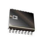
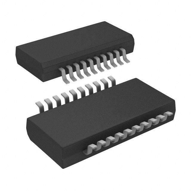
| 供应商器件封装 | 16-TSSOP |
| 信噪比 | 48 dB |
| 分辨率 | 8 bit |
| 包装 | 管件 |
| 商标 | Analog Devices |
| 安装类型 | 表面贴装 |
| 安装风格 | SMD/SMT |
| 封装 | Tube |
| 封装/外壳 | 16-TSSOP(0.173",4.40mm 宽) |
| 封装/箱体 | TSSOP-16 |
| 工作温度 | -40°C ~ 125°C |
| 工作电源电压 | 5 V |
| 工厂包装数量 | 96 |
| 接口类型 | Parallel |
| 数据接口 | 并联 |
| 最大功率耗散 | 17.5 mW |
| 最大工作温度 | + 105 C |
| 最小工作温度 | - 40 C |
| 标准包装 | 96 |
| 特性 | - |
| 电压参考 | External |
| 电压源 | 单电源 |
| 系列 | AD7819 |
| 结构 | SAR |
| 转换器数 | 1 |
| 转换器数量 | 1 |
| 转换速率 | 200 kS/s |
| 输入数和类型 | 1 个单端,单极 |
| 输入类型 | Single-Ended |
| 通道数量 | 1 Channel |
| 采样率(每秒) | 200k |


- 商务部:美国ITC正式对集成电路等产品启动337调查
- 曝三星4nm工艺存在良率问题 高通将骁龙8 Gen1或转产台积电
- 太阳诱电将投资9.5亿元在常州建新厂生产MLCC 预计2023年完工
- 英特尔发布欧洲新工厂建设计划 深化IDM 2.0 战略
- 台积电先进制程称霸业界 有大客户加持明年业绩稳了
- 达到5530亿美元!SIA预计今年全球半导体销售额将创下新高
- 英特尔拟将自动驾驶子公司Mobileye上市 估值或超500亿美元
- 三星加码芯片和SET,合并消费电子和移动部门,撤换高东真等 CEO
- 三星电子宣布重大人事变动 还合并消费电子和移动部门
- 海关总署:前11个月进口集成电路产品价值2.52万亿元 增长14.8%


PDF Datasheet 数据手册内容提取
a 2.7 V to 5.5 V, 200 kSPS 8-Bit Sampling ADC AD7819 FEATURES FUNCTIONAL BLOCK DIAGRAM 8-Bit ADC with 4.5 (cid:1)s Conversion Time On-Chip Track and Hold VDD AGND VREF Operating Supply Range: 2.7 V to 5.5 V Specifications at 2.7 V – 3.6 V and 5 V (cid:2) 10% AD7819 DB7 8-Bit Parallel Interface CHARGE REDISTRIBUTION THREE- 8-Bit Read DAC STATE DRIVERS Power Performance Normal Operation CLOCK DB0 OSC 10.5 mW, V = 3 V DD Automatic Power-Down COMP CONTROL 57.75 (cid:1)W @ 1 kSPS, VDD = 3 V VIN T/H LOGIC Analog Input Range: 0 V to V REF Reference Input Range: 1.2 V to V DD BUSY CS RDCONVST GENERAL DESCRIPTION PRODUCT HIGHLIGHTS The AD7819 is a high speed, microprocessor-compatible, 8-bit 1. Low Power, Single Supply Operation analog-to-digital converter with a maximum throughput of The AD7819 operates from a single 2.7 V to 5.5 V supply 200 kSPS. The converter operates off a single 2.7 V to 5.5 V and typically consumes only 10.5 mW of power. The power supply and contains a 4.5 µs successive approximation A/D dissipation can be significantly reduced at lower through- converter, track/hold circuitry, on-chip clock oscillator and 8-bit put rates by using the automatic power-down mode. wide parallel interface. The parallel interface is designed to 2. Automatic Power-Down allow easy interfacing to microprocessors and DSPs. Using only The automatic power-down mode, whereby the AD7819 address decoding logic the AD7819 is easily mapped into the goes into power-down mode at the end of a conversion and microprocessor address space. powers up before the next conversion, means the AD7819 When used in its power-down mode, the AD7819 automatically is ideal for battery powered applications; e.g., 57.75 µW powers down at the end of a conversion and powers up at the @ 1 kSPS. (See Power vs. Throughput Rate section.) start of a new conversion. This feature significantly reduces the 3. Parallel Interface power consumption of the part at lower throughput rates. The An easy to use 8-bit wide parallel interface allows interfacing AD7819 can also operate in a high speed mode where the part is to most popular microprocessors and DSPs with minimal not powered down between conversions. In this mode of opera- external circuitry. tion the part is capable of providing 200 kSPS throughput. 4. Dynamic Specifications for DSP Users The part is available in a small, 16-lead 0.3" wide, plastic dual- In addition to the traditional ADC specifications, the AD7819 in-line package (DIP); in a 16-lead, 0.15" wide, narrow body is specified for ac parameters, including signal-to-noise ratio small outline IC (SOIC) and in a 16-lead, narrow body, thin and distortion. shrink small outline package (TSSOP). REV.B Information furnished by Analog Devices is believed to be accurate and reliable. However, no responsibility is assumed by Analog Devices for its use, nor for any infringements of patents or other rights of third parties One Technology Way, P.O. Box 9106, Norwood, MA 02062-9106, U.S.A. which may result from its use. No license is granted by implication or Tel: 781/329-4700 World Wide Web Site: http://www.analog.com otherwise under any patent or patent rights of Analog Devices. Fax: 781/326-8703 © Analog Devices, Inc., 2000
AD7819–SPECIFICATIONS1 (GND = 0 V, VREF = VDD = 3 V (cid:2) 10% to 5 V (cid:2) 10%. All specifications –40(cid:3)C to +125(cid:3)C unless otherwise noted.) Parameter Y Version Unit Test Conditions/Comments DYNAMIC PERFORMANCE f = 30 kHz, f = 136 kHz IN SAMPLE Signal to (Noise + Distortion) Ratio1 48 dB min Total Harmonic Distortion (THD)1 –70 dB typ Peak Harmonic or Spurious Noise1 –70 dB typ Intermodulation Distortion2 fa = 29.1 kHz; fb = 29.8 kHz 2nd Order Terms –77 dB typ 3rd Order Terms –77 dB typ DC ACCURACY Resolution 8 Bits Minimum Resolution for Which No Missing Codes Are Guaranteed 8 Bits Relative Accuracy1 ±0.5 LSB max Differential Nonlinearity (DNL)1 ±0.5 LSB max Total Unadjusted Error1 ±1 LSB max Gain Error1 ±0.5 LSB max Offset Error1 ±0.5 LSB max ANALOG INPUT Input Voltage Range 0 V min V V max REF Input Leakage Current2 ±1 µA max Input Capacitance2 15 pF mx REFERENCE INPUTS2 V Input Voltage Range 1.2 V min REF V V max DD Input Leakage Current ±1 µA max Input Capacitance 20 pF max LOGIC INPUTS2 V Input High Voltage 2.0 V min INH, V Input Low Voltage 0.4 V max (0.8 V max, V = 5 V) INL, DD Input Current, I ±1 µA max Typically 10 nA, V = 0 V to V IN IN DD Input Capacitance, C 8 pF max IN LOGIC OUTPUTS Output High Voltage, V 2.4 V min I = 200 µA OH SOURCE Output Low Voltage, V 0.4 V max I = 200 µA OL SINK High Impedance Leakage Current ±1 µA max High Impedance Capacitance 15 pF max CONVERSION RATE Conversion Time 4.5 µs max Track/Hold Acquisition Time1 100 ns max See DC Acquisition Section POWER SUPPLY V 2.7–5.5 Volts For Specified Performance DD I Digital Inputs = 0 V or V DD DD Normal Operation 3.5 mA max Power-Down 1 µA max V = 5 V DD Power Dissipation Normal Operation 17.5 mW max V = 5 V DD Power-Down 5 µW max Auto Power-Down (Mode 2) V = 3 V DD 1 kSPS Throughput 57.75 µW max 10 kSPS Throughput 577.5 µW max 50 kSPS Throughput 2.89 mW max NOTES 1See Terminology section. 2Sample tested during initial release and after any redesign or process change that may affect this parameter. Specifications subject to change without notice. –2– REV. B
AD7819 TIMING CHARACTERISTICS1, 2 (–40(cid:3)C to +125(cid:3)C, unless otherwise noted) Parameter V = 3 V (cid:2) 10% V = 5 V (cid:2) 10% Unit Conditions/Comments DD DD t 1.5 1.5 µs (max) Power-Up Time of AD7819 after Rising Edge of CONVST. POWER-UP t 4.5 4.5 µs (max) Conversion Time. 1 t 30 30 ns (min) CONVST Pulsewidth. 2 t 30 30 ns (max) CONVST Falling Edge to BUSY Rising Edge Delay. 3 t 0 0 ns (min) CS to RD Setup Time. 4 t 0 0 ns (min) CS Hold Time after RD High. 5 t 3 10 10 ns (max) Data Access Time after RD Low. 6 t 3, 4 10 10 ns (max) Bus Relinquish Time after RD High. 7 t 3 100 100 ns (min) Data Bus Relinquish to Falling Edge of CONVST Delay. 8 NOTES 1Sample tested to ensure compliance. 2See Figures 12, 13 and 14. 3These numbers are measured with the load circuit of Figure 1. They are defined as the time required for the o/p to cross 0.8 V or 2.4 V for V = 5 V ± 10% and DD 0.4 V or 2 V for V = 3 V ± 10%. DD 4Derived from the measured time taken by the data outputs to change 0.5 V when loaded with the circuit of Figure 1. The measured number is then extrapolated back to remove the effects of charging or discharging the 50 pF capacitor. This means that the time, t , quoted in the Timing Characteristics is the true bus relinquish time 7 of the part and as such is independent of external bus loading capacitances. Specifications subject to change without notice. ABSOLUTE MAXIMUM RATINGS* VDD to DGND . . . . . . . . . . . . . . . . . . . . . . . . . –0.3 V to +7 V 200(cid:1)A IOL Digital Input Voltage to DGND (CONVST, RD, CS) . . . . . . . . . . . . . .–0.3 V, V + 0.3 V DD TO Digital Output Voltage to DGND OUTPUT 1.6V (BUSY, DB0–DB7) . . . . . . . . . . . . . . .–0.3 V, VDD + 0.3 V PIN 50CpFL REF to AGND . . . . . . . . . . . . . . . . . . . –0.3 V, V + 0.3 V IN DD Analog Input . . . . . . . . . . . . . . . . . . . . . .–0.3 V, VDD + 0.3 V 200(cid:1)A IOH Storage Temperature Range . . . . . . . . . . . . –65°C to +150°C Junction Temperature . . . . . . . . . . . . . . . . . . . . . . . . . .150°C Figure 1.Load Circuit for Digital Output Timing Plastic DIP Package, Power Dissipation . . . . . . . . . . 450 mW Specifications θ Thermal Impedance . . . . . . . . . . . . . . . . . . . . 105°C/W JA Lead Temperature, (Soldering 10 sec) . . . . . . . . . . . .260°C ORDERING GUIDE SOIC Package, Power Dissipation . . . . . . . . . . . . . . . 450 mW θJA Thermal Impedance . . . . . . . . . . . . . . . . . . . . . 75°C/W Linearity Lead Temperature, Soldering Error Package Package Vapor Phase (60 sec) . . . . . . . . . . . . . . . . . . . . . . .215°C Model (LSB) Description Option Infrared (15 sec) . . . . . . . . . . . . . . . . . . . . . . . . . .220°C AD7819YN ±1 LSB Plastic DIP N-16 SSOP Package, Power Dissipation . . . . . . . . . . . . . . . 450 mW θ Thermal Impedance . . . . . . . . . . . . . . . . . . . . 115°C/W AD7819YR ±1 LSB Small Outline IC R-16A JA AD7819YRU ±1 LSB Thin Shrink Small Outline RU-16 Lead Temperature, Soldering Vapor Phase (60 sec) . . . . . . . . . . . . . . . . . . . . . . .215°C (TSSOP) Infrared (15 sec) . . . . . . . . . . . . . . . . . . . . . . . . . .220°C *Stresses above those listed under Absolute Maximum Ratings may cause perma- nent damage to the device. This is a stress rating only; functional operation of the device at these or any other conditions above those listed in the operational sections of this specification is not implied. Exposure to absolute maximum rating conditions for extended periods may affect device reliability. CAUTION ESD (electrostatic discharge) sensitive device. Electrostatic charges as high as 4000 V readily WARNING! accumulate on the human body and test equipment and can discharge without detection. Although the AD7819 features proprietary ESD protection circuitry, permanent damage may occur on devices subjected to high-energy electrostatic discharges. Therefore, proper ESD precautions are recommended to avoid performance degradation or loss of functionality. ESD SENSITIVE DEVICE REV. B –3–
AD7819 PIN FUNCTION DESCRIPTIONS Pin No. Mnemonic Description 1 V Reference Input, 1.2 V to V . REF DD 2 V Analog Input, 0 V to V . IN REF 3 GND Analog and Digital Ground. 4 CONVST Convert Start. A low-to-high transition on this pin initiates a 1.5 µs pulse on an internally generated CONVST signal. A high-to-low transition on this line initiates the conversion process if the internal CONVST signal is low. Depending on the signal on this pin at the end of a conversion, the AD7819 automatically powers down. 5 CS Chip Select. This is a logic input. CS is used in conjunction with RD to enable outputs. 6 RD Read Pin. This is a logic input. When CS is low and RD goes low, the DB7–DB0 leave their high impedance state and data is driven onto the data bus. 7 BUSY ADC Busy Signal. This is a logic output. This signal goes logic high during the conversion process. 8–15 DB0–DB7 Data Bit 0 to 7. These outputs are three-state TTL-compatible. 16 V Positive power supply voltage, 2.7 V to 5.5 V. DD PIN CONFIGURATION DIP/SOIC VREF 1 16 VDD VIN 2 15 DB7 GND 3 14 DB6 AD7819 CONVST 4 13 DB5 TOP VIEW CS 5 12 DB4 (Not to Scale) RD 6 11 DB3 BUSY 7 10 DB2 DB0 8 9 DB1 –4– REV. B
AD7819 TERMINOLOGY The AD7819 is tested using the CCIF standard, where two Signal to (Noise + Distortion) Ratio input frequencies near the top end of the input bandwidth are This is the measured ratio of signal to (noise + distortion) at the used. In this case, the second and third order terms are of different output of the A/D converter. The signal is the rms amplitude of significance. The second order terms are usually distanced in the fundamental. Noise is the rms sum of all nonfundamental frequency from the original sine waves, while the third order signals up to half the sampling frequency (f /2), excluding dc. terms are usually at a frequency close to the input frequencies. S The ratio is dependent upon the number of quantization levels As a result, the second and third order terms are specified sepa- in the digitization process; the more levels, the smaller the quan- rately. The calculation of the intermodulation distortion is as tization noise. The theoretical signal to (noise + distortion) per the THD specification where it is the ratio of the rms sum ratio for an ideal N-bit converter with a sine wave input is given of the individual distortion products to the rms amplitude of by: the fundamental expressed in dBs. Signal to (Noise + Distortion) = (6.02N + 1.76) dB Relative Accuracy Relative accuracy or endpoint nonlinearity is the maximum Thus for an 8-bit converter, this is 50dB. deviation from a straight line passing through the endpoints of Total Harmonic Distortion the ADC transfer function. Total harmonic distortion (THD) is the ratio of the rms sum of Differential Nonlinearity harmonics to the fundamental. For the AD7819 it is defined as: This is the difference between the measured and the ideal 1LSB change between any two adjacent codes in the ADC. THD(dB)=20log V22+V32+V42+V52+V62 Offset Error V1 This is the deviation of the first code transition (0000...000) where V is the rms amplitude of the fundamental and V , V , to (0000...001) from the ideal, i.e., AGND + 1 LSB. 1 2 3 V4, V5 and V6 are the rms amplitudes of the second through the Offset Error Match sixth harmonics. This is the difference in Offset Error between any two channels. Peak Harmonic or Spurious Noise Gain Error Peak harmonic or spurious noise is defined as the ratio of the This is the deviation of the last code transition (1111...110) rms value of the next largest component in the ADC output to (1111...111) from the ideal, i.e., VREF – 1 LSB, after the spectrum (up to fS/2 and excluding dc) to the rms value of the offset error has been adjusted out. fundamental. Normally, the value of this specification is deter- Gain Error Match mined by the largest harmonic in the spectrum, but for parts This is the difference in Gain Error between any two channels. where the harmonics are buried in the noise floor, it will be a noise peak. Track/Hold Acquisition Time Track/hold acquisition time is the time required for the output Intermodulation Distortion of the track/hold amplifier to reach its final value, within With inputs consisting of sine waves at two frequencies, fa and ±1/2 LSB, after the end of conversion (the point at which the fb, any active device with nonlinearities will create distortion track/hold returns to track mode). It also applies to situations products at sum and difference frequencies of mfa ± nfb where where a change in the selected input channel takes place or m, n = 0, 1, 2, 3, etc. Intermodulation terms are those for which where there is a step input change on the input voltage applied neither m nor n are equal to zero. For example, the second order to the selected V input of the AD7819. It means that the user terms include (fa + fb) and (fa – fb), while the third order terms IN must wait for the duration of the track/hold acquisition time include (2fa + fb), (2fa – fb), (fa + 2fb) and (fa – 2fb). after the end of conversion or after a step input change to V IN before starting another conversion, to ensure that the part operates to specification. REV. B –5–
AD7819 CIRCUIT DESCRIPTION SUPPLY Converter Operation 2.7V TO 5.5V 10(cid:1)F 0.1(cid:1)F The AD7819 is a successive approximation analog-to-digital PARALLEL converter based around a charge redistribution DAC. The ADC VDD VREF INTERFACE DB0-DB7 can convert analog input signals in the range 0 V to V . Fig- DD AD7819 uFrigesu r2e a2n sdh 3o wbse ltohwe AshDowC sdiumrpinligf ieitds ascchqeumisaittiiocns opfh athsee. ASDWC2. is 0V TOIN VPRUETF VIN BUSY (cid:1)C/(cid:1)P RD closed and SW1 is in Position A, the comparator is held in a GND CS balanced condition and the sampling capacitor acquires the sig- nal on V . CONVST IN+ Figure 4.Typical Connection Diagram CHARGE RESTRIBUTION Analog Input DAC SAMPLING Figure 5 shows an equivalent circuit of the analog input struc- A CAPACITOR ture of the AD7819. The two diodes, D1 and D2, provide ESD VIN CONTROL SW1 LOGIC protection for the analog inputs. Care must be taken to ensure B ACQUISITION SW2 that the analog input signal never exceeds the supply rails by PHASE COMPARATOR more than 200 mV. This will cause these diodes to become AGND VDD/3 COLOSCCK forward biased and start conducting current into the substrate. 20 mA is the maximum current these diodes can conduct with- out causing irreversible damage to the part. The capacitor C2 Figure 2.ADC Track Phase is typically about 4 pF and can be primarily attributed to pin When the ADC starts a conversion, see Figure 3, SW2 will open capacitance. The resistor R1 is a lumped component made up of and SW1 will move to Position B causing the comparator to the on resistance of a multiplexer and a switch. This resistor is become unbalanced. The Control Logic and the Charge Redis- typically about 125 Ω. The capacitor C1 is the ADC sampling tribution DAC are used to add and subtract fixed amounts of capacitor and has a capacitance of 3.5 pF. charge from the sampling capacitor to bring the comparator back into a balanced condition. When the comparator is rebal- VDD anced the conversion is complete. The Control Logic generates the ADC output code. Figure 7 shows the ADC transfer function. D1 R1 C1 125(cid:5) 3.5pF CHARGE VIN VDD/3 RESTRIBUTION C2 DAC 4pF D2 CONVERT PHASE – SWITCH OPEN SAMPLING TRACK PHASE – SWITCH CLOSED A CAPACITOR VIN CONTROL SW1B CONVERSION SW2 LOGIC Figure 5.Equivalent Analog Input Circuit PHASE COMPARATOR DC Acquisition Time AGND VDD/3 COLOSCCK The ADC starts a new acquisition phase at the end of a conver- sion and ends on the falling edge of the CONVST signal. At the Figure 3.ADC Conversion Phase end of a conversion there is a settling time associated with the sampling circuit. This settling time lasts approximately 100 ns. TYPICAL CONNECTION DIAGRAM The analog signal on V is also being acquired during this IN Figure 4 shows a typical connection diagram for the AD7819. The settling time. The minimum acquisition time needed is approxi- parallel interface is implemented using an 8-bit data bus, the mately 100 ns. Figure 6 shows the equivalent charging circuit falling edge of CONVST brings the BUSY signal high and at for the sampling capacitor when the ADC is in its acquisition the end of conversion, the falling edge of BUSY is used to phase. R2 represents the source impedance of a buffer amplifier initiate an ISR on a microprocessor. (See Parallel Interface or resistive network, R1 is an internal multiplexer resistance and section for more details.) VREF is connected to a well decoupled C1 is the sampling capacitor. V pin to provide an analog input range of 0 V to V . When DD DD V is first connected the AD7819 powers up in a low current DD R1 mode, i.e., power-down. A rising edge on the CONVST input R2 VIN 125(cid:5) will cause the part to power up. (See Power-Up Times section.) C1 If power consumption is of concern, the automatic power-down 3.5pF at the end of a conversion should be used to improve power performance. See Power vs. Throughput Rate section of the Figure 6.Equivalent Sampling Circuit data sheet. –6– REV. B
AD7819 During the acquisition phase the sampling capacitor must be When operating in Mode 2, the ADC is powered down at the charged to within a 1/2 LSB of its final value. The time it takes end of each conversion and powered up again before the next to charge the sampling capacitor (T ) is given by the fol- conversion is initiated. (See Figure 8.) CHARGE lowing formula: T = 6.2 × (R2 + 125 Ω) × 3.5 pF MODE 1 CHARGE For small values of source impedance, the settling time associ- VDD ated with the sampling circuit (100 ns) is, in effect, the acquisition EXT CONVST time of the ADC. For example, with a source impedance (R2) t of 10 Ω, the charge time for the sampling capacitor is approxi- PO1W.5E(cid:1)Rs-UP mately 3 ns. The charge time becomes significant for source impedances of 2 kΩ and greater. INT CONVST AC Acquisition Time In ac applications it is recommended to always buffer analog MODE 2 input signals. The source impedance of the drive circuitry must VDD be kept as low as possible to minimize the acquisition time of the ADC. Large values of source impedance will cause the THD to EXT CONVST degrade at high throughput rates. tPOWER-UP tPOWER-UP 1.5(cid:1)s 1.5(cid:1)s ADC TRANSFER FUNCTION INT CONVST The output coding of the AD7819 is straight binary. The designed code transitions occur at successive integer LSB values (i.e., Figure 8.Power-Up Times 1 LSB, 2 LSBs, etc.). The LSB size is = V /256. The ideal REF transfer characteristic for the AD7819 is shown in Figure 7 below. POWER VS. THROUGHPUT RATE By operating the AD7819 in Mode 2, the average power con- sumption of the AD7819 decreases at lower throughput rates. 111...111 Figure 9 shows how the Automatic Power-Down is implemented 111...110 • using the external CONVST signal to achieve the optimum • DE 111..•.000 power performance for the AD7819. The AD7819 is operated C CO 011..••.111 1LSB = VREF/256 in Mode 2 and the duration of the external CONVST pulse is D • set to be equal to or less than the power-up time of the device. A • • As the throughput rate is reduced, the device remains in its power- 000...010 000...001 down state longer and the average power consumption over time 000...000 drops accordingly. 0V1LSB +VREF –1LSB ANALOG INPUT Figure 7.Transfer Characteristic EXT CONVST t POWER-UP TIMES POWER-UP The AD7819 has a 1.5 µs power-up time. When V is first con- 1.5(cid:1)s tC4O.N5(cid:1)VEsRT POWER-DOWN DD nected, the AD7819 is in a low current mode of operation. In INT CONVST order to carry out a conversion the AD7819 must first be pow- t ered up. The ADC is powered up by a rising edge on an internally CYCLE 100(cid:1)s @ 10kSPS generated CONVST signal, which occurs as a result of a rising edge on the external CONVST pin. The rising edge of the external Figure 9.Automatic Power-Down CONVST signal initiates a 1.5 µs pulse on the internal CONVST If, for example, the AD7819 is operated in a continuous sam- signal. This pulse is present to ensure the part has enough time pling mode with a throughput rate of 10 kSPS, the power to power-up before a conversion is initiated, as a conversion is consumption is calculated as follows. The power dissipation initiated on the falling edge of gated CONVST. See Timing and during normal operation is 10.5 mW, V = 3 V. If the power- DD Control section. Care must be taken to ensure that the CONVST up time is 1.5 µs and the conversion time is 4.5 µs, the AD7819 pin of the AD7819 is logic low when VDD is first applied. can be said to dissipate 10.5 mW for 6 µs (worst case) during each conversion cycle. If the throughput rate is 10 kSPS, the cycle time is then 100 µs and the average power dissipated dur- ing each cycle is (6/100) × (10.5 mW) = 630 µW. REV. B –7–
AD7819 Typical Performance Characteristics external CONVST and this internal CONVST are input to an OR gate. The resultant signal has the duration of the longer of the two input signals. Once a conversion has been initiated, the 10 BUSY signal goes high to indicate a conversion is in progress. At the end of conversion the sampling circuit returns to its track- ing mode. The end of conversion is indicated by the BUSY signal going low. This signal may be used to initiate an ISR on a 1 microprocessor. At this point the conversion result is latched W m into the output register where it may be read. The AD7819 has R – an 8-bit wide parallel interface. The state of the external CONVST E W signal at the end of conversion also establishes the mode of O P operation of the AD7819. 0.1 Mode 1 Operation (High Speed Sampling) If the external CONVST is logic high when BUSY goes low, the part is said to be in Mode 1 operation. While operating in Mode 0.01 1 the AD7819 will not power down between conversions. The 0 5 10 15 20 25 30 35 40 45 50 AD7819 should be operated in Mode 1 for high speed sam- THROUGHPUT – kSPS pling applications, i.e., throughputs greater than 100 kSPS. Figure 10.Power vs. Throughput Figure 13 shows the timing for Mode 1 operation. From this diagram one can see that a minimum delay of the sum of the 0 conversion time and read time must be left between two succes- AD7819 –10 2048 POINT FFT sive falling edges of the external CONVST. This is to ensure that –20 SFIANM =P 2L9I.N96G1 1k3H6z.054kHz a conversion is not initiated during a read. –30 Mode 2 Operation (Automatic Power-Down) At slower throughput rates the AD7819 may be powered down –40 between conversion to give a superior power performance. dBs –50 This is Mode 2 Operation and it is achieved by bringing the –60 CONVST signal logic low before the falling edge of BUSY. Fig- –70 ure 14 shows the timing for Mode 2 Operation. The falling edge of the external CONVST signal may occur before or after the –80 falling edge of the internal CONVST signal, but it is the later –90 occurring falling edge of both that controls when the first conver- –100 sion will take place. If the falling edge of the external CONVST 0 7 13 20 27 33 40 47 53 60 66 FREQUENCY – kHz occurs after that of the internal CONVST, it means that the Figure 11.SNR moment of the first conversion is controlled exactly, regardless of any jitter associated with the internal CONVST signal. The parallel interface is still fully operational while the AD7819 is TIMING AND CONTROL The AD7819 has only one input for timing and control, i.e., powered down. The AD7819 is powered up again on the rising the CONVST (convert start signal). The rising edge of this edge of the CONVST signal. The gated CONVST pulse will CONVST signal initiates a 1.5 µs pulse on an internally gener- now remain high long enough for the AD7819 to fully power ated CONVST signal. This pulse is present to ensure the part up, which takes about 1.5µs. This is ensured by the internal has enough time to power up before a conversion is initiated. If CONVST signal, which will remain high for 1.5 µs. the external CONVST signal is low, the falling edge of the in- ternal CONVST signal will cause the sampling circuit to go into hold mode and initiate a conversion. If, however, the external CONVST EXT CONVST signal is high when the internal CONVST goes low, (PIN 4) GATED it is upon the falling edge of the external CONVST signal that INT the sampling circuitry will go into hold mode and initiate a conversion. The use of the internally generated 1.5 µs pulse as 1.5(cid:1)s previously described can be likened to the configuration shown Figure 12. in Figure 12. The application of a CONVST signal at the CONVST pin triggers the generation of a 1.5 µs pulse. Both the –8– REV. B
AD7819 t 1 t 2 EXT CONVST t 3 t POWER-UP INT CONVST BUSY CS/RD DB7–DB0 8 MSBs Figure 13.Mode 1 Operation EXT CONVST t POWER-UP t 1 INT CONVST t 3 BUSY CS/RD DB7–DB0 8 MSBs Figure 14.Mode 2 Operation PARALLEL INTERFACE BUSY goes logic high. Care must be taken to ensure that a read The parallel interface of the AD7819 is eight bits wide. The out- operation does not occur while BUSY is high. Data read from put data buffers are activated when both CS and RD are logic the AD7819 while BUSY is high will be invalid. For optimum low. At this point the contents of the data register are placed on performance the read operation should end at least 100 ns (t) the 8-bit data bus. Figure 15 shows the timing diagram for the par- 8 prior to the falling edge of the next CONVST. allel port. The Parallel Interface of the AD7819 is reset when CONVST t 2 t3 t8 BUSY t 1 CS t t 4 5 RD t 7 t 6 DB7–DB0 8 MSBs Figure 15.Parallel Port Timing REV. B –9–
AD7819 MICROPROCESSOR INTERFACING The parallel port on the AD7819 allows the device to be inter- faced to a range of many different microcontrollers. This section PSP0–PSP7 DB0–DB7 explains how to interface the AD7819 with some of the more common microcontroller parallel interface protocols. PIC16C6x/7x* AD7819* AD7819 to 8051 CS CS Figure 16 shows a parallel interface between the AD7819 and the 8051 microcontroller. The BUSY signal on the AD7819 pro- vides an interrupt request to the 8051 when a conversion begins. RD RD Port 0 of the 8051 may serve as an input or output port, or as in this case when used together, may be used as a bidirectional INT BUSY low-order address and data bus. The address latch enable out- put of the 8051 is used to latch the low byte of the address *ADDITIONAL PINS OMITTED FOR CLARITY during accesses to the device, while the high-order address byte Figure 17.Interfacing to the PIC16C6x/7x is supplied from Port 2. Port 2 latches remain stable when the AD7819 is addressed, as they do not have to be turned around AD7819 to ADSP-21xx (set to 1) for data input as is the case for Port 0. Figure 18 shows a parallel interface between the AD7819 and the ADSP-21xx series of DSPs. As before, the BUSY signal on the AD7819 provides an interrupt request to the DSP when a conversion begins. 8051* DB0–DB7 AD0–AD7 LATCH AD7819* D0–D7 DB0–DB7 DECODER ALE A13–A0 CS AD7819* A8–A15 ADSP-21xx* ADDRESS DECODE RD RD LOGIC INT BUSY DMS EN CS *ADDITIONAL PINS OMITTED FOR CLARITY RD RD IRQ BUSY Figure 16.Interfacing to the 8051 AD7819 to PIC16C6x/7x *ADDITIONAL PINS OMITTED FOR CLARITY Figure 17 shows a parallel interface between the AD7819 and the Figure 18.Interfacing to the ADSP-21xx PIC16C64/65/74. The BUSY signal on the AD7819 provides an interrupt request to the microcontroller when a conversion begins. Of the PIC16C6x/7x range of microcontrollers, only the PIC16C64/65/74 can provide the option of a parallel slave port. Port D of the microcontroller will operate as an 8-bit wide parallel slave port when control bit PSPMODE in the TRISE register is set. Setting PSPMODE enables the port pin RE0 to be the RD output and RE2 to be the CS output. For this functionality, the corresponding data direction bits of the TRISE register must be configured as outputs (reset to 0). See user PIC16/17 Microcontroller User Manual. –10– REV. B
AD7819 OUTLINE DIMENSIONS Dimensions shown in inches and (mm). 16-Lead Plastic DIP (N-16) 0.840 (21.33) B) 0.745 (18.93) v. e 16 9 0.280 (7.11) 0 (r 1 8 0.240 (6.10) 0.325 (8.25) 0/0 0.300 (7.62)0.195 (4.95) –1 PIN 1 0.060 (1.52) 0.115 (2.93) –0 0.210 (5.33) 0.015 (0.38) 318 MAX 0.130 01 0.160 (4.06) (3.30) C 0.115 (2.93) MIN 0.015 (0.381) 0.022 (0.558) 0.100 0.070 (1.77) SEATING 0.008 (0.204) 0.014 (0.356) (2.54) 0.045 (1.15) PLANE BSC 16-Lead Small Outline Package (R-16A) 0.3937 (10.00) 0.3859 (9.80) 16 9 0.1574 (4.00) 0.2550 (6.20) 0.1497 (3.80) 1 8 0.2284 (5.80) PIN 1 0.0688 (1.75) 0.0196 (0.50) 0.0098 (0.25) 0.0532 (1.35) 0.0099 (0.25)x 45° 0.0040 (0.10) 8° SEATING 0(.10.52070) 00..00119328 ((00..4395)) 0.0099 (0.25)0° 0.0500 (1.27) PLANE 0.0075 (0.19) 0.0160 (0.41) BSC 16-Lead Thin Shrink Small Outline Package (RU-16) 0.201 (5.10) 0.193 (4.90) 16 9 0.177 (4.50) 0.169 (4.30) 1 0.256 (6.50) 0.246 (6.25) 8 A. S. PIN 1 U. 0.006 (0.15) N 0.002 (0.05) 0.0433 D I E (1.10) T MAX 8° 0.028 (0.70) N SEATING 0(.00.26556) 00..00101785 ((00..3109)) 0.0079 (0.20)0° 0.020 (0.50) PRI PLANE BSC 0.0035 (0.090) REV. B –11–
Mouser Electronics Authorized Distributor Click to View Pricing, Inventory, Delivery & Lifecycle Information: A nalog Devices Inc.: AD7819YRZ-REEL7 AD7819YRZ AD7819YRUZ-REEL7 AD7819YNZ AD7819YRUZ AD7819YRUZ-REEL