ICGOO在线商城 > 集成电路(IC) > 数据采集 - 模数转换器 > ADS8328IBPW
 Datasheet下载
- 型号: ADS8328IBPW
- 制造商: Texas Instruments
- 库位|库存: xxxx|xxxx
- 要求:
| 数量阶梯 | 香港交货 | 国内含税 |
| +xxxx | $xxxx | ¥xxxx |
查看当月历史价格
查看今年历史价格
ADS8328IBPW产品简介:
ICGOO电子元器件商城为您提供ADS8328IBPW由Texas Instruments设计生产,在icgoo商城现货销售,并且可以通过原厂、代理商等渠道进行代购。 ADS8328IBPW价格参考¥51.40-¥85.72。Texas InstrumentsADS8328IBPW封装/规格:数据采集 - 模数转换器, 16 Bit Analog to Digital Converter 2 Input 1 SAR 16-TSSOP。您可以下载ADS8328IBPW参考资料、Datasheet数据手册功能说明书,资料中有ADS8328IBPW 详细功能的应用电路图电压和使用方法及教程。
Texas Instruments(德州仪器)的ADS8328IBPW是一款16位分辨率、低功耗的模数转换器(ADC),属于数据采集系统中的关键组件。其应用场景主要包括以下几个方面:

1. 工业自动化与控制
   ADS8328IBPW适用于工业自动化设备,如可编程逻辑控制器(PLC)、数据采集模块和过程控制系统。它能够将传感器采集到的模拟信号(如温度、压力、流量等)转换为数字信号,以便后续处理和分析。

2. 医疗设备
   在医疗领域,该器件可用于心电图(ECG)、血压监测仪、血糖仪等设备中。高精度的16位分辨率使其能够准确捕捉微弱的生理信号,确保诊断结果的可靠性。

3. 测试与测量仪器
   该ADC适合用于示波器、信号分析仪和数据记录仪等测试设备。其低功耗特性和高性能表现,能够满足对精度和效率要求较高的测量需求。

4. 能源管理与电力监控
   ADS8328IBPW可用于智能电网、电表和电源管理系统中,用于监测电压、电流和功率等参数。其稳定的性能有助于实现精确的能量计量和故障检测。

5. 环境监测与物联网
   在环境监测领域,这款ADC可以集成到气象站、水质检测仪和空气质量监测设备中,用于采集温度、湿度、气体浓度等数据。同时,它也适用于物联网(IoT)边缘节点的数据采集任务。

总结来说,ADS8328IBPW凭借其高精度、低功耗和小封装尺寸的优势,广泛应用于需要可靠模拟信号数字化的各种场景,尤其是在对精度和能效有严格要求的工业、医疗和测试领域中表现出色。
| 参数 | 数值 |
| 产品目录 | 集成电路 (IC)半导体 |
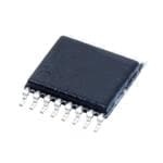
| 描述 | IC ADC 16BIT 500KSPS DUAL16TSSOP模数转换器 - ADC 2.7-5.5V 16-Bit 500KSPS Serial ADC |
| 产品分类 | |
| 品牌 | Texas Instruments |
| 产品手册 | |
| 产品图片 |
|
| rohs | 符合RoHS无铅 / 符合限制有害物质指令(RoHS)规范要求 |
| 产品系列 | 数据转换器IC,模数转换器 - ADC,Texas Instruments ADS8328IBPW- |
| 数据手册 | |
| 产品型号 | ADS8328IBPW |
| PCN设计/规格 | |
| 产品培训模块 | http://www.digikey.cn/PTM/IndividualPTM.page?site=cn&lang=zhs&ptm=13240http://www.digikey.cn/PTM/IndividualPTM.page?site=cn&lang=zhs&ptm=25729 |
| 产品目录页面 | |
| 产品种类 | 模数转换器 - ADC |
| 位数 | 16 |
| 供应商器件封装 | 16-TSSOP |
| 信噪比 | 91 dB |
| 其它名称 | 296-19765 |
| 分辨率 | 16 bit |
| 制造商产品页 | http://www.ti.com/general/docs/suppproductinfo.tsp?distId=10&orderablePartNumber=ADS8328IBPW |
| 包装 | 管件 |
| 单位重量 | 62 mg |
| 商标 | Texas Instruments |
| 安装类型 | 表面贴装 |
| 安装风格 | SMD/SMT |
| 封装 | Tube |
| 封装/外壳 | 16-TSSOP(0.173",4.40mm 宽) |
| 封装/箱体 | TSSOP-16 |
| 工作温度 | -40°C ~ 85°C |
| 工作电源电压 | 5 V |
| 工厂包装数量 | 90 |
| 接口类型 | Serial, SPI |
| 数据接口 | DSP,串行,SPI™ |
| 最大功率耗散 | 38.5 mW |
| 最大工作温度 | + 85 C |
| 最小工作温度 | - 40 C |
| 标准包装 | 90 |
| 特性 | - |
| 电压参考 | External |
| 电压源 | 模拟和数字 |
| 系列 | ADS8328 |
| 结构 | SAR |
| 转换器数 | 1 |
| 转换器数量 | 1 |
| 转换速率 | 500 kS/s |
| 输入数和类型 | 1 个伪差分,单极 |
| 输入类型 | Pseudo-Differential |
| 通道数量 | 2 Channel |
| 采样率(每秒) | 500k |


- 商务部:美国ITC正式对集成电路等产品启动337调查
- 曝三星4nm工艺存在良率问题 高通将骁龙8 Gen1或转产台积电
- 太阳诱电将投资9.5亿元在常州建新厂生产MLCC 预计2023年完工
- 英特尔发布欧洲新工厂建设计划 深化IDM 2.0 战略
- 台积电先进制程称霸业界 有大客户加持明年业绩稳了
- 达到5530亿美元!SIA预计今年全球半导体销售额将创下新高
- 英特尔拟将自动驾驶子公司Mobileye上市 估值或超500亿美元
- 三星加码芯片和SET,合并消费电子和移动部门,撤换高东真等 CEO
- 三星电子宣布重大人事变动 还合并消费电子和移动部门
- 海关总署:前11个月进口集成电路产品价值2.52万亿元 增长14.8%


PDF Datasheet 数据手册内容提取
ADS8327 ADS8328 www.ti.com SLAS415E–APRIL2006–REVISEDJANUARY2011 LOW POWER, 16-BIT, 500-kHz, SINGLE/DUAL UNIPOLAR INPUT, ANALOG-TO-DIGITAL CONVERTERS WITH SERIAL INTERFACE CheckforSamples:ADS8327,ADS8328 FEATURES APPLICATIONS 1 • 2.7-Vto5.5-VAnalogSupply,LowPower: • Communications – 10.6mW(500kHz,+VA=2.7V, • TransducerInterface +VBD=1.8V) • MedicalInstruments • 500-kHzSamplingRate • Magnetometers • ExcellentDCPerformance • IndustrialProcessControl • DataAcquisitionSystems – ±1.5LSBTyp, ±2LSBMaxINL • AutomaticTestEquipment – ±0.6LSBTyp, ±1LSBMaxDNL – 16-BitNMCOverTemperature DESCRIPTION – ±0.5mVMaxOffsetErrorat2.7V The ADS8327 is a low power, 16-bit, 500-kSPS – ±1mVMaxOffsetErrorat5V analog-to-digital converter with a unipolar input. The • ExcellentACPerformanceatf =10kHzwith device includes a 16-bit capacitor-based SAR A/D I 91dBSNR,100dBSFDR,–96dBTHD converterwithinherentsampleandhold. • Built-InConversionClock(CCLK) The ADS8328 is based on the same core and • 1.65Vto1.5×(+VA)I/OSupply includes a 2-to-1 input MUX with programmable option of TAG bit output. Both the ADS8327 and – SPI/DSPCompatibleSerial ADS8328 offer a high-speed, wide voltage serial – SCLKupto50MHz interface and are capable of chain mode operation • ComprehensivePower-DownModes: whenmultipleconvertersareused. – DeepPower-Down These converters are available in a 16-lead TSSOP – NapPower-Down or 4x4 QFN packages and are fully specified for operation over the industrial –40°C to +85°C – AutoNapPower-Down temperaturerange. • UnipolarInputRange:0VtoV REF • SoftwareReset Table1.LowPower,High-SpeedSARConverter Family • GlobalCONVST(IndependentofCS) • ProgrammableStatus/PolarityEOC/INT Type/Speed 500kHz 1MHz Single ADS8327 ADS8329 • 16-Pin4×4QFNor16-PinTSSOPPackages 16BitPseudo-Diff Dual ADS8328 ADS8330 • Multi-ChipDaisyChainMode • ProgrammableTAGBitOutput • Auto/ManualChannelSelectMode OUTPUT ADS8328 ADS8327 SAR LATCH SDO and +IN1 NC 3−STATE DRIVER + +IN0 +IN _ CDAC FS/CS CONVERSION SCLK COM −IN COMPARATOR and SDI CONTROL REF+ OSC LOGIC CONVST REF− EOC/INT/CDI 1 Pleasebeawarethatanimportantnoticeconcerningavailability,standardwarranty,anduseincriticalapplicationsofTexas Instrumentssemiconductorproductsanddisclaimerstheretoappearsattheendofthisdatasheet. PRODUCTIONDATAinformationiscurrentasofpublicationdate. ©2006–2011,TexasInstrumentsIncorporated Products conform to specifications per the terms of the Texas Instruments standard warranty. Production processing does not necessarilyincludetestingofallparameters.
ADS8327 ADS8328 SLAS415E–APRIL2006–REVISEDJANUARY2011 www.ti.com This integrated circuit can be damaged by ESD. Texas Instruments recommends that all integrated circuits be handled with appropriateprecautions.Failuretoobserveproperhandlingandinstallationprocedurescancausedamage. ESDdamagecanrangefromsubtleperformancedegradationtocompletedevicefailure.Precisionintegratedcircuitsmaybemore susceptibletodamagebecauseverysmallparametricchangescouldcausethedevicenottomeetitspublishedspecifications. ORDERINGINFORMATION(1) MAXIMUM MAXIMUM MAXIMUM TRANSPORT INTEGRAL DIFFERENTIAL OFFSET PACKAGE PACKAGE TEMPERATURE ORDERING MODEL MEDIA LINEARITY LINEARITY ERROR TYPE DESIGNATOR RANGE INFORMATION QUANTITY (LSB) (LSB) (mV) ADS8327IPW Tube90 TSSOP-16 PW Tapeandreel ADS8327IPWR 2000 ADS8327I ±3 –1/+2 ±1.25 –40°Cto+85°C Smalltapeand ADS8327IRSAT reel250 4×4QFN-16 RSA Tapeandreel ADS8327IRSAR 3000 ADS8327IBPW Tube90 TSSOP-16 PW Tapeandreel ADS8327IBPWR 2000 ADS8327IB ±2 ±1 ±1 –40°Cto+85°C Smalltapeand ADS8327IBRSAT reel250 4×4QFN-16 RSA Tapeandreel ADS8327IBRSAR 3000 ADS8328IPW Tube90 TSSOP-16 PW Tapeandreel ADS8328IPWR 2000 ADS8328I ±3 –1/+2 ±1.25 –40°Cto+85°C Smalltapeand ADS8328IRSAT reel250 4×4QFN-16 RSA Tapeandreel ADS8328IRSAR 3000 ADS8328IBPW Tube90 TSSOP-16 PW Tapeandreel ADS8328IBPWR 2000 ADS8328IB ±2 ±1 ±1 –40°Cto+85°C Smalltapeand ADS8328IBRSAT reel250 4×4QFN-16 RSA Tapeandreel ADS8328IBRSAR 3000 (1) Forthemostcurrentpackageandorderinginformation,seethePackageOptionAddendumattheendofthisdocument,orvisitthe deviceproductfolderatwww.ti.com. 2 SubmitDocumentationFeedback ©2006–2011,TexasInstrumentsIncorporated ProductFolderLink(s):ADS8327ADS8328
ADS8327 ADS8328 www.ti.com SLAS415E–APRIL2006–REVISEDJANUARY2011 ABSOLUTE MAXIMUM RATINGS Overoperatingfree-airtemperaturerange,unlessotherwisenoted.(1) UNIT +INtoAGND –0.3Vto+VA+0.3V Voltage –INtoAGND –0.3Vto+VA+0.3V +VAtoAGND –0.3Vto7V +REFtoAGND –0.3Vto+VA+0.3V Voltagerange –REFtoAGND –0.3Vto+0.3V +VBDtoBDGND –0.3Vto7V AGNDtoBDGND –0.3Vto0.3V DigitalinputvoltagetoBDGND –0.3Vto+VBD+0.3V DigitaloutputvoltagetoBDGND –0.3Vto+VBD+0.3V T Operatingfree-airtemperaturerange –40°Cto+85°C A T Storagetemperaturerange –65°Cto+150°C stg Junctiontemperature(T max) +150°C J TSSOP-16 Powerdissipation (TJMax-TA)/qJA Package q thermalimpedance 86°C/W JA 4×4QFN-16 Powerdissipation (TJMax–TA)/qJA Package q thermalimpedance 47°C/W JA (1) Stressesbeyondthoselistedunderabsolutemaximumratingsmaycausepermanentdamagetothedevice.Thesearestressratings only,andfunctionaloperationofthedeviceattheseoranyotherconditionsbeyondthoseindicatedunderrecommendedoperating conditionsisnotimplied.Exposuretoabsolute-maximum-ratedconditionsforextendedperiodsmayaffectdevicereliability. ©2006–2011,TexasInstrumentsIncorporated SubmitDocumentationFeedback 3 ProductFolderLink(s):ADS8327ADS8328
ADS8327 ADS8328 SLAS415E–APRIL2006–REVISEDJANUARY2011 www.ti.com SPECIFICATIONS T =–40°Cto85°C,+VA=2.7Vto3.6V,+VBD=1.65Vto1.5×(+VA),V =2.5V,andf =500kHz,unless A REF SAMPLE otherwisenoted. PARAMETER TESTCONDITIONS MIN TYP MAX UNIT ANALOGINPUT Full-scaleinputvoltage(1) +IN–(–IN)or(+INx–COM) 0 +VREF V +IN,+IN0,+IN1 AGND–0.2 +VA+0.2 Absoluteinputvoltage V –INorCOM AGND–0.2 AGND+0.2 Inputcapacitance 40 45 pF Noongoingconversion, Inputleakagecurrent –1 1 nA DCInput Atdc 108 Inputchannelisolation,ADS8328only dB VI=±1.25VPPat50kHz 101 SYSTEMPERFORMANCE Resolution 16 Bits Nomissingcodes 16 Bits ADS8327IB, –2 ±1.2 2 INL Integrallinearity ADS8328IB LSB(2) ADS8327I,ADS8328I –3 ±2 3 ADS8327IB, DNL Differential ADS8328IB –1 ±0.6 1 LSB(2) linearity ADS8327I,ADS8328I –1 ±1 2 ADS8327IB, –0.5 ±0.1 0.5 EO Offseterror(3) ADS8328IB mV ADS8327I,ADS8328I –0.8 ±0.1 0.8 Offseterrordrift 0.2 ppm/°C EG Gainerror –0.25 –0.07 0.25 %FSR Gainerrordrift 0.3 ppm/°C Atdc 70 CMRR Common-moderejectionratio dB VI=0.4VPPat1MHz 50 Noise 33 mVRMS PSRR Power-supplyrejectionratio AtFFFFhoutputcode(3) 78 dB SAMPLINGDYNAMICS tCONV Conversiontime 18 CCLK tSAMPLE1 Manualtrigger 3 Acquisitiontime CCLK tSAMPLE2 Autotrigger 3 Throughputrate 500 kHz Aperturedelay 5 ns Aperturejitter 10 ps Stepresponse 100 ns Overvoltagerecovery 100 ns (1) Idealinputspan,doesnotincludegainoroffseterror. (2) LSBmeansleastsignificantbit. (3) Measuredrelativetoanidealfull-scaleinput[+IN–(–IN)]of2.5Vwhen+VA=2.7V. 4 SubmitDocumentationFeedback ©2006–2011,TexasInstrumentsIncorporated ProductFolderLink(s):ADS8327ADS8328
ADS8327 ADS8328 www.ti.com SLAS415E–APRIL2006–REVISEDJANUARY2011 SPECIFICATIONS (continued) T =–40°Cto85°C,+VA=2.7Vto3.6V,+VBD=1.65Vto1.5×(+VA),V =2.5V,andf =500kHz,unless A REF SAMPLE otherwisenoted. PARAMETER TESTCONDITIONS MIN TYP MAX UNIT DYNAMICCHARACTERISTICS THD Totalharmonicdistortion(4) VIN=2.5VPPat10kHz –98 dB VIN=2.5VPPat100kHz –83.5 VIN=2.5VPPat10kHz 88.5 SNR Signal-to-noiseratio dB VIN=2.5VPPat100kHz 85 VIN=2.5VPPat10kHz 88.5 SINAD Signal-to-noise+distortion dB VIN=2.5VPPat100kHz 81 VIN=2.5VPPat10kHz 101 SFDR Spurious-freedynamicrange dB VIN=2.5VPPat100kHz 84 –3dBsmall-signalbandwidth 30 MHz CLOCK Internalconversionclockfrequency 10.5 11 12.2 MHz UsedasI/Oclockonly 33 SCLKExternalserialclock MHz AsI/Oclockandconversionclock 1 21 EXTERNALVOLTAGEREFERENCEINPUT Inputreference VREF(REF+–REF–) 3.6V≥+VA≥2.7V 0.3 2.525 VREF range (REF–)–AGND –0.1 0.1 V Resistance(5) Referenceinput 80 kΩ DIGITALINPUT/OUTPUT Logicfamily—CMOS VIH High-levelinputvoltage (+VA×1.5)V≥+VBD≥1.65V 0.65×(+VBD) +VBD+0.3 V VIL Low-levelinputvoltage (+VA×1.5)V≥+VBD≥1.65V –0.3 0.35×(+VBD) V II Inputcurrent VI=+VBDorBDGND –50 50 nA CI Inputcapacitance 5 pF (+VA×1.5)V≥+VBD≥1.65V, VOH High-leveloutputvoltage IO=100mA +VBD–0.6 +VBD V (+VA×1.5)V≥+VBD≥1.65V, VOL Low-leveloutputvoltage IO=100mA 0 0.4 V CO Outputcapacitance 5 pF CL Loadcapacitance 30 pF Dataformat—straightbinary POWER-SUPPLYREQUIREMENTS Power-supply +VBD 1.65 +VA 1.5×(+VA) V voltage +VA 2.7 3.6 V 500-kHzSamplerate 3.8 5 mA Supplycurrent NAP/Auto-NAPmode 0.2 0.4 Deeppower-downmode 2 50 nA BufferI/Osupplycurrent 500kSPS 0.2 mA Powerdissipation +VA=2.7V,+VBD=1.8V 10.6 14 mW TEMPERATURERANGE TA Operatingfree-airtemperature –40 +85 °C (4) Calculatedonthefirstnineharmonicsoftheinputfrequency. (5) Canvary±30%. ©2006–2011,TexasInstrumentsIncorporated SubmitDocumentationFeedback 5 ProductFolderLink(s):ADS8327ADS8328
ADS8327 ADS8328 SLAS415E–APRIL2006–REVISEDJANUARY2011 www.ti.com SPECIFICATIONS T =–40°Cto85°C,+VA=4.5Vto5.5V,+VBD=1.65Vto5.5V,V =4.096V,andf =500kHz,unlessotherwise A REF SAMPLE noted. PARAMETER TESTCONDITIONS MIN TYP MAX UNIT ANALOGINPUT Full-scaleinputvoltage(1) +IN–(–IN)or(+INx–COM) 0 +VREF V +IN,+IN0,+IN1 AGND–0.2 +VA+0.2 Absoluteinputvoltage V –INorCOM AGND–0.2 AGND+0.2 Inputcapacitance 40 45 pF Noongoingconversion, Inputleakagecurrent –1 1 nA DCInput Atdc 109 Inputchannelisolation,ADS8328only dB VI=±1.25VPPat50kHz 101 SYSTEMPERFORMANCE Resolution 16 Bits Nomissingcodes 16 Bits ADS8327IB, –2 ±1.5 2 INL Integrallinearity ADS8328IB LSB(2) ADS8327I,ADS8328I –3 ±2 3 ADS8327IB, DNL Differential ADS8328IB –1 ±0.7 1 LSB(2) linearity ADS8327I,ADS8328I –1 ±1 2 ADS8327IB, –1 ±0.4 1 EO Offseterror(3) ADS8328IB mV ADS8327I,ADS8328I –1.25 ±0.4 1.25 Offseterrordrift 0.5 ppm/°C EG Gainerror –0.25 –0.07 0.25 %FSR Gainerrordrift 0.3 ppm/°C Atdc 70 CMRR Common-moderejectionratio dB VI=1VPPat1MHz 50 Noise 33 mVRMS PSRR Power-supplyrejectionratio AtFFFFhoutputcode(3) 78 dB SAMPLINGDYNAMICS tCONV Conversiontime 18 CCLK tSAMPLE Manualtrigger 3 1 Acquisitiontime CCLK tSAMPLE Autotrigger 3 2 Throughputrate 500 kHz Aperturedelay 5 ns Aperturejitter 10 ps Stepresponse 100 ns Overvoltagerecovery 100 ns (1) Idealinputspan,doesnotincludegainoroffseterror. (2) LSBmeansleastsignificantbit. (3) Measuredrelativetoanidealfull-scaleinput[+IN–(–IN)]of4.096Vwhen+VA=5V. 6 SubmitDocumentationFeedback ©2006–2011,TexasInstrumentsIncorporated ProductFolderLink(s):ADS8327ADS8328
ADS8327 ADS8328 www.ti.com SLAS415E–APRIL2006–REVISEDJANUARY2011 SPECIFICATIONS (continued) T =–40°Cto85°C,+VA=4.5Vto5.5V,+VBD=1.65Vto5.5V,V =4.096V,andf =500kHz,unlessotherwise A REF SAMPLE noted. PARAMETER TESTCONDITIONS MIN TYP MAX UNIT DYNAMICCHARACTERISTICS VIN=4.096VPPat10kHz -96 THD Totalharmonicdistortion(4) VIN=4.096VPPat100kHz, ADS8327/28IB –95.7 dB VIN=4.096VPPat100kHz, ADS8327/28I –95.7 VIN=4.096VPPat10kHz 91 SNR Signal-to-noiseratio dB VIN=4.096VPPat100kHz 89 VIN=4.096VPPat10kHz 91 SINAD Signal-to-noise+distortion dB VIN=4.096VPPat100kHz 88 VIN=4.096VPPat10kHz 100 SFDR Spurious-freedynamicrange VIN=4.096VPPat100kHz, ADS8327/28IB 98.8 dB VIN=4.096VPPat100kHz, ADS8327/28I 98.8 –3dBSmall-signalbandwidth 30 MHz CLOCK Internalconversionclockfrequency 10.9 12 12.6 MHz UsedasI/Oclockonly 50 SCLKExternalserialclock MHz AsI/Oclockandconversionclock 1 21 EXTERNALVOLTAGEREFERENCEINPUT Inputreference VREF(REF+–REF–) 5.5V≥+VA≥4.5V 0.3 4.096 4.2 VREF range (REF–)–AGND –0.1 0.1 V Resistance(5) Referenceinput 80 kΩ DIGITALINPUT/OUTPUT Logicfamily—CMOS VIH High-levelinputvoltage 5.5V≥+VBD≥4.5V 0.65×(+VBD) +VBD+0.3 V VIL Low-levelinputvoltage 5.5V≥+VBD≥4.5V –0.3 0.35×(+VBD) V II Inputcurrent VI=+VBDorBDGND -50 50 nA CI Inputcapacitance 5 pF 5.5V≥+VBD≥4.5V, VOH High-leveloutputvoltage IO=100mA +VBD–0.6 +VBD V 5.5V≥+VBD≥4.5V, VOL Low-leveloutputvoltage IO=100mA 0 0.4 V CO Outputcapacitance 5 pF CL Loadcapacitance 30 pF Dataformat—straightbinary POWER-SUPPLYREQUIREMENTS Powersupply +VBD 1.65 3.3 5.5 V voltage +VA 4.5 5 5.5 V 500-kHzSamplerate 5 6.2 mA Supplycurrent NAP/Auto-NAPmode 0.3 0.5 Deeppower-downmode 6 50 nA BufferI/Osupplycurrent 500kSPS 1 mA +VA=5V,+VBD=5V 30 38.5 Powerdissipation mW +VA=5V,+VBD=1.8V 25.4 32 TEMPERATURERANGE TA Operatingfree-airtemperature –40 +85 °C (4) Calculatedonthefirstnineharmonicsoftheinputfrequency. (5) Canvary±30% ©2006–2011,TexasInstrumentsIncorporated SubmitDocumentationFeedback 7 ProductFolderLink(s):ADS8327ADS8328
ADS8327 ADS8328 SLAS415E–APRIL2006–REVISEDJANUARY2011 www.ti.com TIMING CHARACTERISTICS Allspecificationstypicalat–40°Cto85°C,+VA=2.7v,+VBD=1.8V(1) (2) PARAMETER MIN TYP MAX UNIT External, 0.5 10.5 f =1/2f CCLK SCLK fCCLK Frequency,conversionclock,CCLK Internal MHz f =1/2f 10.5 11 12.2 CCLK SCLK t Setuptime,fallingedgeofCStoEOC 1 CCLK su(CSF-EOC) t Holdtime,fallingedgeofCStoEOC 0 ns h(CSF-EOC) t Pulseduration,CONVSTlow 40 ns wL(CONVST) t Setuptime,fallingedgeofCStoEOS 20 ns su(CSF-EOS) t Holdtime,fallingedgeofCStoEOS 20 ns h(CSF-EOS) t Setuptime,risingedgeofCStoEOS 20 ns su(CSR-EOS) t Holdtime,risingedgeofCStoEOS 20 ns h(CSR-EOS) Setuptime,fallingedgeofCStofirstfalling t 5 ns su(CSF-SCLK1F) SCLK t Pulseduration,SCLKlow 8 t –8 ns wL(SCLK) c(SCLK) t Pulseduration,SCLKhigh 8 t –8 ns wH(SCLK) c(SCLK) I/OClockonly 30 I/Oandconversionclock 47.6 2000 tc(SCLK) Cycletime,SCLK I/OClock,chainmode 30 ns I/Oandconversionclock, 47.6 2000 chainmode Delaytime,fallingedgeofSCLKtoSDO t 10-pFLoad 7.5 ns d(SCLKF-SDOINVALID) invalid Delaytime,fallingedgeofSCLKtoSDO t 10-pFLoad 16 ns d(SCLKF-SDOVALID) valid Delaytime,fallingedgeofCStoSDOvalid, t 10-pFLoad 13 ns d(CSF-SDOVALID) SDOMSBoutput t Setuptime,SDItofallingedgeofSCLK 8 ns su(SDI-SCLKF) t Holdtime,SDItofallingedgeofSCLK 4 ns h(SDI-SCLKF) Delaytime,risingedgeofCS/FStoSDO t 8 ns d(CSR-SDOZ) 3-state Setuptime,16thfallingedgeofSCLK t 10 ns su(16thSCLKF-CSR) beforerisingedgeofCS/FS Delaytime,CDIhightoSDOhighindaisy t 10-pFLoad,chainmode 25 ns d(SDO-CDI) chainmode (1) Allinputsignalsarespecifiedwitht =t =1.5ns(10%to90%ofV )andtimedfromavoltagelevelof(V +V )/2. r f DD IL IH (2) Seetimingdiagrams. 8 SubmitDocumentationFeedback ©2006–2011,TexasInstrumentsIncorporated ProductFolderLink(s):ADS8327ADS8328
ADS8327 ADS8328 www.ti.com SLAS415E–APRIL2006–REVISEDJANUARY2011 TIMING CHARACTERISTICS Allspecificationstypicalat–40°Cto85°C,+VA=+VBD=5V (1) (2) PARAMETER MIN TYP MAX UNIT External, 0.5 10.5 f =1/2f CCLK SCLK fCCLK Frequency,conversionclock,CCLK Internal MHz f =1/2f 10.9 12 12.6 CCLK SCLK t Setuptime,fallingedgeofCStoEOC 1 CCLK su(CSF-EOC) t Holdtime,fallingedgeofCStoEOC 0 ns h(CSF-EOC) t Pulseduration,CONVSTlow 40 ns wL(CONVST) t Setuptime,fallingedgeofCStoEOS 20 ns su(CSF-EOS) t Holdtime,fallingedgeofCStoEOS 20 ns h(CSF-EOS) t Setuptime,risingedgeofCStoEOS 20 ns su(CSR-EOS) t Holdtime,risingedgeofCStoEOS 20 ns h(CSR-EOS) Setuptime,fallingedgeofCStofirstfalling t 5 ns su(CSF-SCLK1F) SCLK t Pulseduration,SCLKlow 8 t –8 ns wL(SCLK) c(SCLK) t Pulseduration,SCLKhigh 8 t –8 ns wH(SCLK) c(SCLK) I/OClockonly 20 I/Oandconversionclock 47.6 2000 tc(SCLK) Cycletime,SCLK I/OClock,chainmode 20 ns I/Oandconversionclock, 47.6 2000 chainmode Delaytime,fallingedgeofSCLKtoSDO t 10-pFLoad 2 ns d(SCLKF-SDOINVALID) invalid Delaytime,fallingedgeofSCLKtoSDO t 10-pFLoad 10 ns d(SCLKF-SDOVALID) valid Delaytime,fallingedgeofCStoSDO t 10-pFLoad 8.5 ns d(CSF-SDOVALID) valid,SDOMSBoutput t Setuptime,SDItofallingedgeofSCLK 8 ns su(SDI-SCLKF) t Holdtime,SDItofallingedgeofSCLK 4 ns h(SDI-SCLKF) Delaytime,risingedgeofCS/FStoSDO t 5 ns d(CSR-SDOZ) 3-state Setuptime,16thfallingedgeofSCLK t 10 ns su(16thSCLKF-CSR) beforerisingedgeofCS/FS Delaytime,CDIhightoSDOhighin t 10-pFLoad,chainmode 16 ns d(SDO-CDI) daisy-chainmode (1) Allinputsignalsarespecifiedwitht =t =1.5ns(10%to90%ofV )andtimedfromavoltagelevelof(V +V )/2. r f DD IL IH (2) Seetimingdiagrams. ©2006–2011,TexasInstrumentsIncorporated SubmitDocumentationFeedback 9 ProductFolderLink(s):ADS8327ADS8328
ADS8327 ADS8328 SLAS415E–APRIL2006–REVISEDJANUARY2011 www.ti.com PIN ASSIGNMENTS ADS8327 ADS8328 PW PACKAGE PW PACKAGE (TOP VIEW) (TOP VIEW) +VA 1 16 +VBD +VA 1 16 +VBD RESERVED 2 15 SCLK +IN1 2 15 SCLK +IN 3 14 BDGND +IN0 3 14 BDGND −IN 4 13 SDO COM 4 13 SDO AGND 5 12 SDI AGND 5 12 SDI REF− 6 11 FS/CS REF− 6 11 FS/CS REF+ (REFIN) 7 10 EOC/INT REF+ (REFIN) 7 10 EOC/INT NC 8 9 CONVST NC 8 9 CONVST NC − No internal connection ADS8327 ADS8328 RSA PACKAGE RSA PACKAGE (TOP VIEW) (TOP VIEW) EF− GND N N EF− GND OM N0 R A −I +I R A C +I 16 15 14 13 16 15 14 13 REF+(REFIN) 1 12 RESERVED REF+(REFIN) 1 12 +IN1 NC 2 11 +VA NC 2 11 +VA CONVST 3 10 +VBD CONVST 3 10 +VBD EOC/INT/CDI 4 9 SCLK EOC/INT/CDI 4 9 SCLK 5 6 7 8 5 6 7 8 S DI O D S DI O D C S D N C S D N S/ S G S/ S G F D F D B B NC − No internal connection CAUTION: The thermal pad is internally connected to the substrate. This pad can be connected to the analog ground or left floating. Keep the thermal pad separate from the digital ground, if possible. 10 SubmitDocumentationFeedback ©2006–2011,TexasInstrumentsIncorporated ProductFolderLink(s):ADS8327ADS8328
ADS8327 ADS8328 www.ti.com SLAS415E–APRIL2006–REVISEDJANUARY2011 ADS8327TerminalFunctions NO. NAME I/O DESCRIPTION TSSOP QFN AGND 5 15 – Analogground BDGND 14 8 – Interfaceground CONVST 9 3 I Freezessampleandhold,startsconversionwithnextrisingedgeofinternalclock Statusoutput.IfprogrammedasEOC,thispinislow(default)whenaconversionisin progress.Ifprogrammedasaninterrupt(INT),thispinislowforapreprogrammed EOC/INT/CDI 10 4 O durationaftertheendofconversionandvaliddataaretobeoutput.ThepolarityofEOC orINTisprogrammable.Thispincanalsobeusedasachaindatainputwhenthedevice isoperatedinchainmode. I FramesyncsignalforTMS320DSPserialinterfaceorchipselectinputforSPIinterface FS/CS 11 5 slaveselect(SS–). +IN 3 13 I Noninvertinginput –IN 4 14 I Invertinginput,usuallyconnectedtoground NC 8 2 Noconnection REF+ 7 1 I Externalreferenceinput. REF– 6 16 I ConnecttoAGNDthroughindividualvia. RESERVED 2 12 – Reserved,connecttoAGNDor+VA SCLK 15 9 I Clockforserialinterface SDI 12 6 I Serialdatain SDO 13 7 O Serialdataout +VA 1 11 Analogsupply,+2.7Vto+5.5VDC. +VBD 16 10 Interfacesupply ADS8328TerminalFunctions NO. NAME I/O DESCRIPTION TSSOP QFN AGND 5 15 – Analogground BDGND 14 8 – Interfaceground COM 4 14 I Commoninvertinginput,usuallyconnectedtoground CONVST 9 3 I Freezessampleandhold,startsconversionwithnextrisingedgeofinternalclock Statusoutput.IfprogrammedasEOC,thispinislow(default)whenaconversionisin progress.Ifprogrammedasaninterrupt(INT),thispinislowforapreprogrammed EOC/INT/ 10 4 O durationaftertheendofconversionandvaliddataaretobeoutput.ThepolarityofEOC CDI orINTisprogrammable.Thispincanalsobeusedasachaindatainputwhenthedevice isoperatedinchainmode. FS/CS 11 5 I FramesyncsignalforTMS320DSPserialinterfaceorchipselectinputforSPIinterface +IN1 2 12 I Secondnoninvertinginput. +IN0 3 13 I Firstnoninvertinginput NC 8 2 – Noconnection. REF+ 7 1 I Externalreferenceinput. REF– 6 16 I ConnecttoAGNDthroughindividualvia. SCLK 15 9 I Clockforserialinterface SDI 12 6 I Serialdatain(conversionstartandresetpossible) SDO 13 7 O Serialdataout +VA 1 11 Analogsupply,+2.7Vto+5.5VDC. +VBD 16 10 Interfacesupply ©2006–2011,TexasInstrumentsIncorporated SubmitDocumentationFeedback 11 ProductFolderLink(s):ADS8327ADS8328
ADS8327 ADS8328 SLAS415E–APRIL2006–REVISEDJANUARY2011 www.ti.com MANUALTRIGGER / READ While Sampling (use internal CCLK, EOC andINTpolarity programmed as active low) CONVST Nth t wL(CONVST) OC OS OC OS EOC E E Nth E E (active low) t = 3 CCLKs min t = 18 CCLKs SAMPLE1 CONV t = 3 CCLKs min SAMPLE1 INT (active low) t t h(CSR-EOS) h(CSF-EOC) t h(CSF-EOC) t t h(CSF-EOS) su(CSF-EOC) t su(CSF-EOS) CS/FS 1 SCLK 1 . . . . . . . . . . . . . . . . . . . . 16 t = 20 ns min d(CSR-EOS) SDO Nth−1st Nth SDI 1101b 1101b READ Result READ Result Figure1. TimingforConversionandAcquisitionCyclesforManualTrigger(ReadWhileSampling) AUTO TRIGGER / READ While Sampling (use internal CCLK, EOC andINTpolarity programmed as active low) CONVST= 1 EOC EOS EOC EOS Nth EOC EOS (active low) t = 18 CCLKs t = 3 CCLKs t = 18 CCLKs t = 3 CCLKs CONV SAMPLE2 CONV SAMPLE2 INT (active low) t t h(CSF-EOS) h(CSF-EOC) t t su(CSF-EOS) su(CSF-EOS) CS/FS SCLK 1 . . . . . . . . . . . . . . . . . . .16 1 . . . . . . . . . . . . . . . . . . .16 t 1 h(CSF-EOC) SDO N−2nd N−1st Nth SDI 1110b. . . . . . . . . . . . . . 1101b 1101b CONFIGURE READ Result READ Result Figure2. TimingforConversionandAcquisitionCyclesforAutotrigger(ReadWhileSampling) 12 SubmitDocumentationFeedback ©2006–2011,TexasInstrumentsIncorporated ProductFolderLink(s):ADS8327ADS8328
ADS8327 ADS8328 www.ti.com SLAS415E–APRIL2006–REVISEDJANUARY2011 MANUALTRIGGER / READ While Converting (use internal CCLK, EOC andINTpolarity programmed as active low) CONVST Nth N + 1st t wL(CONVST) S C S O Nth O O N + 1st E E E EOC (active low) tCONV = 18 CCLKs tSAMPLE1 = 3 CCLKs min INT (active low) t h(CSF-EOS) t t su(CSF-EOS) su(CSR-EOS) CS/FS tsu(CSF-EOC) th(CSF-EOC) SCLK 1 . . . . . . . . . . . . . . . . . . . .16 1 SDO N−1st N th SDI 1101b 1101b READ Result READ Result Figure3. TimingforConversionandAcquisitionCyclesforManualTrigger(ReadWhileConverting) AUTO TRIGGER / READ While Converting (use internal CCLK, EOC andINTpolarity programmed as active low) CONVST= 1 EOC EOS EOC EOS N + 1st EOC EOS (active low) t = 18 CCLKs t = 18 CCLKs CONV CONV t = 3 CCLKs min t = 3 CCLKs min Nth SAMPLE2 SAMPLE2 INT (active low) tsu(CSF-EOS) th(CSF-EOS) t tsu(CSR-EOS) t h(CSF-EOS) h(CSR-EOS) CS/FS 1 . . . . . . . . . . . . . . . . . . 16 SCLK 1 . . . . . . . . . . . . . . . . . . .16 1 . . . . . . . . . . . . . . . . . . 16 tsu(CSR-EOS) SDO N−2nd ?? N−1st Nth SDI 1110b . . . . . . . . . . . . . . . 1101b 1101b CONFIGURE READ Result READ Result Figure4. TimingforConversionandAcquisitionCyclesforAutotrigger(ReadWhileConverting) ©2006–2011,TexasInstrumentsIncorporated SubmitDocumentationFeedback 13 ProductFolderLink(s):ADS8327ADS8328
ADS8327 ADS8328 SLAS415E–APRIL2006–REVISEDJANUARY2011 www.ti.com 1 2 3 4 5 6 7 14 15 16 SCLK tc(SCLK) tsu(CSF−SCLK1F) twH(SCLK) tsu(16thSCLK−CSR) twL(SCLK) CS/FS td(SCLKF−SDOINVALID) td(CSR−SDOZ) td(CSF−SDOVALID) td(SCLKF−SDOVALID) Hi−Z SDO MSB MSB−1 MSB−2 MSB−3 MSB−4 MSB−5 MSB−6 LSB+2 LSB+1 LSB th(SDI−SCLKF) SDI MSB MSB−1 MSB−2 MSB−3 MSB−4 MSB−5 MSB−6 LSB+2 LSB+1 LSB tsu(SDI−SCLKF) Figure5. DetailedSPITransferTiming MANUALTRIGGER / READ While Sampling (use internal CCLKactive high, EOC andINTactive low, TAG enabled, auto channel select) Nth CH0 Nth CH1 CONVST t t wL(CONVST) wL(CONVST) C S O O EOC E E Nth CH0 Nth CH1 (active low) tCONV = 18 CCLKs tCONV = 18 CCLKs t = 3 CCLKs min SAMPLE1 INT (active low) t su(CSF-EOS) t h(CSF-EOC) CS/FS SCLK 1. . . . . . . . . . . . . . . . . . . . . . .16 17 1 . . . . . . . . . . . . . . . . . . . . . . . 16 17 t =20 ns MIN d(CSR-EOS) Hi−Z Hi−Z SDO N−1th CH1 Nth CH0 TAG = 1 TAG = 0 SDI 1101b 1101b READ Result READ Result Figure6. SimplifiedDualChannelTiming 14 SubmitDocumentationFeedback ©2006–2011,TexasInstrumentsIncorporated ProductFolderLink(s):ADS8327ADS8328
ADS8327 ADS8328 www.ti.com SLAS415E–APRIL2006–REVISEDJANUARY2011 TYPICAL CHARACTERISTICS At –40°C to 85°C, V (REF+ – REF–) = 4.096 V when +VA = +VBD = 5 V or V (REF+ – REF–) = 2.5 V REF REF when +VA = +VBD = 2.7 V, f = 21 MHz, f = DC for DC curves, and f = 100 kHz for AC curves, unless SCLK I I otherwisenoted. CROSSTALK DIFFERENTIALNONLINEARITY INTEGRALNONLINEARITY vs vs vs FREQUENCY FREE-AIRTEMPERATURE FREE-AIRTEMPERATURE 110 0.9 1.8 105 0.8 1.7 +VA= 5 V 100 B Crosstalk - d 9905 +VA= 5 V DNL- LSB 0.7 +VA= 2.7 INL- LSB 1.6 +VA= 5 V 0.6 1.5 85 +VA= 2.7 V +VA= 2.7 80 0.5 1.4 0 50 100 150 200 -40 -25 -10 5 20 35 50 65 80 -40 -25 -10 5 20 35 50 65 80 F -Frequency - kHz TA- Free-Air Temperature - °C TA- Free-Air Temperature - °C Figure7. Figure8. Figure9. DIFFERENTIALNONLINEARITY INTEGRALNONLINEARITY DIFFERENTIALNONLINEARITY vs vs vs EXTERNALCLOCKFREQUENCY EXTERNALCLOCKFREQUENCY EXTERNALCLOCKFREQUENCY 2 2 2 +VA= 5 V +VA= 5 V +VA= 2.7 V 1.5 1.5 1.5 Max 1 MAX 1 1 Max 0.5 0.5 0.5 DNL- LSB-0.50 MIN INL- LSB -0.50 DNL- LSB -0.05 Min -1 -1 -1 Min -1.5 -1.5 -1.5 -2 -2 -2 0 5 10 15 20 0 5 10 15 20 0 5 10 15 20 External Clock Frequency - MHz External Clock Frequency - MHz External Clock Frequency - MHz Figure10. Figure11. Figure12. ©2006–2011,TexasInstrumentsIncorporated SubmitDocumentationFeedback 15 ProductFolderLink(s):ADS8327ADS8328
ADS8327 ADS8328 SLAS415E–APRIL2006–REVISEDJANUARY2011 www.ti.com TYPICAL CHARACTERISTICS (continued) INTEGRALNONLINEARITY OFFSETVOLTAGE OFFSETVOLTAGE vs vs vs EXTERNALCLOCKFREQUENCY FREE-AIRTEMPERATURE SUPPLYVOLTAGE 2 1 1 +VA= 2.7 V 1.5 Max 0.8 0.8 1 V V INL- LSB-00-..5051 Min Offset Voltage - m 00..46 +VA= 5 V Offset Voltage - m 00..46 0.2 +VA= 2.7 0.2 -1.5 -2 0 0 0 5 10 15 20 25 -40 -25 -10 5 20 35 50 65 80 2.7 3.2 3.7 4.2 4.7 5.2 External Clock Frequency - MHz TA- Free-Air Temperature - °C +VA- Supply Voltage - V Figure13. Figure14. Figure15. POWER-SUPPLYREJECTION GAINERROR GAINERROR RATIO vs vs vs FREE-AIRTEMPERATURE SUPPLYVOLTAGE SUPPLYRIPPLEFREQUENCY -0.065 -0.065 -80 B d o - R -0.068 mV -0.068 n Rati -78 Gain Error - % FS --00..007730 +VA= 5 V+VA= 2.7 Offset VoltageChange - --00..007730 R - Power Supply Rejectio ---777642 +VA= 2.7 V +VA= 5 V R -0.075 -0.075 PS -70 -40 -25 -10 5 20 35 50 65 80 2.7 3.2 3.7 4.2 4.7 5.2 0 20 40 60 80 100 TA- Free-Air Temperature - °C +VA- Supply Voltage - V Supply Ripple Frequency - kHz Figure16. Figure17. Figure18. SIGNAL-TO-NOISEAND SIGNAL-TO-NOISERATIO DISTORTION TOTALHARMONICDISTORTION vs vs vs INPUTFREQUENCY INPUTFREQUENCY INPUTFREQUENCY 92 92 -150 B d SNR - Signal-To-Noise Ratio - dB 889680 +VA+=V A5 =V 2.7 V AD - Signal-To-Noise and Distortion - 8888924680 +V+AV=A 2=. 75 VV THD - Total Harmonic Distortion - dB -1---99080055 +VA=+ 2V.7A V= 5 V 840 20 40 60 80 100 SIN 800 20 40 60 80 100 -800 20 40 60 80 100 fi- Input Frequency - kHz fi- Input Frequency - kHz fi- Input Frequency - kHz Figure19. Figure20. Figure21. 16 SubmitDocumentationFeedback ©2006–2011,TexasInstrumentsIncorporated ProductFolderLink(s):ADS8327ADS8328
ADS8327 ADS8328 www.ti.com SLAS415E–APRIL2006–REVISEDJANUARY2011 TYPICAL CHARACTERISTICS (continued) SIGNAL-TO-NOISEAND SPURIOUS-FREEDYNAMICRANGE SIGNAL-TO-NOISERATIO DISTORTION vs vs vs INPUTFREQUENCY FULL-SCALERANGE FULL-SCALERANGE 110 92 B 92 ous Free Dynamic Range - dB 1100990550 +VA= 5 +VVA= 2.7 V Signal-To-Noise Ratio - dB 888048 10 kHz2 .I7n pVut 5 V nal-To-Noise and Distortion - d 888048 10 kHz2 I.n7p Vut 5 V FDR - Spuri 8805 SNR - 7726 SINAD - Sig 7726 S 0 20 40 60 80 100 0 1 2 3 4 5 0 1 2 3 4 5 fi- Input Frequency - kHz Full Scale Range - V Full Scale Range - V Figure22. Figure23. Figure24. TOTALHARMONICDISTORTION SPURIOUS-FREEDYNAMICRANGE TOTALHARMONICDISTORTION vs vs vs FULL-SCALERANGE FULL-SCALERANGE FREE-AIRTEMPERATURE -100 10 kHz Input dB 102 10 KHz -100 THD - Total Harmonic Distortion -dB ---998628 2.7 V 5 V DR - Spurious Free Dynamic Range - 10999902468 2.7 V 5 V THD - Total Harmonic Distortion - dB --9986 +VA=+ V5A V=, 120.70 VkH, 1z0 I nkpHuzt Input SF 90 -94 0 1 2 3 4 5 0 1 2 3 4 5 -40 -25 -10 5 20 35 50 65 80 Full Scale Range - V Full Scale Range - V TA- Free-Air Temperature - °C Figure25. Figure26. Figure27. SIGNAL-TO-NOISEAND SPURIOUS-FREEDYNAMICRANGE SIGNAL-TO-NOISERATIO DISTORTION vs vs vs FREE-AIRTEMPERATURE FREE-AIRTEMPERATURE FREE-AIRTEMPERATURE B 102 92 B 92 d d R - Spurious Free Dynamic Range - 1990680 ++VVAA== 5 2 V.7, 1V0, 01 0k HkHz zIn Ipnuptut SNR - Signal-To-Noise Ratio - dB 98891890 ++VVAA== 52 .V7 ,V 1,0 100 k kHHzz I nInppuutt D - Signal-To-Noise and Distortion - 88998901 ++VVAA== 52 .V7, V1,0 100 k kHHzz I nInppuutt D A SF 94-40 -25 -10 5 20 35 50 65 80 87-40 -25 -10 5 20 35 50 65 80 SIN 87-40 -25 -10 5 20 35 50 65 80 TA- Free-Air Temperature - °C TA- Free-Air Temperature - °C TA- Free-Air Temperature - °C Figure28. Figure29. Figure30. ©2006–2011,TexasInstrumentsIncorporated SubmitDocumentationFeedback 17 ProductFolderLink(s):ADS8327ADS8328
ADS8327 ADS8328 SLAS415E–APRIL2006–REVISEDJANUARY2011 www.ti.com TYPICAL CHARACTERISTICS (continued) EFFECTIVENUMBEROFBITS INTERNALCLOCKFREQUENCY INTERNALCLOCKFREQUENCY vs vs vs FREE-AIRTEMPERATURE SUPPLYVOLTAGE FREE-AIRTEMPERATURE 12 12 s ENOB - Effective Number of Bits - bit 111444...579 +VA= 2.7 V, 1+0V AkH=z 5 I nVp, u1t00 kHz Input Internal Clock Frequency - MHz 11111111....2468 Internal Clock Frequency - MHz 11111111....2468 ++VVAA== 2 5.7 V V 14.3 11.0 11 -40 -25 -10 5 20 35 50 65 80 2.7 3.2 3.7 4.2 4.7 5.2 5.7 -40 -25 -10 5 20 35 50 65 80 TA- Free-Air Temperature - °C +VA- Supply Voltage - V TA- Free-Air Temperature - °C Figure31. Figure32. Figure33. ANALOGSUPPLYCURRENT ANALOGSUPPLYCURRENT ANALOGSUPPLYCURRENT vs vs vs SUPPLYVOLTAGE SUPPLYVOLTAGE SUPPLYVOLTAGE 5.6 320 12 500 kSPS NAPMode PD Mode 300 10 mA 5.1 Am nA Analog Supply Current - 44..16 Analog Supply Current - 222246820000 Analog Supply Current - 2468 3.6 200 0 2.7 3.2 3.7 4.2 4.7 5.2 2.7 3.2 3.7 4.2 4.7 5.2 2.7 3.2 3.7 4.2 4.7 5.2 +VA- Supply Voltage - V +VA- Supply Voltage - V +VA- Supply Voltage - V Figure34. Figure35. Figure36. ANALOGSUPPLYCURRENT ANALOGSUPPLYCURRENT ANALOGSUPPLYCURRENT vs vs vs SAMPLERATE SAMPLERATE FREE-AIRTEMPERATURE 6 400 5.5 500 kSPS Sample Rate Autonap Mode PD Mode 5 A mA 5 +VA= 5 V nalog Supply Current - mA 1234 +VA= 5 V +VA= 2.7 V Analog Supply Current -m 123000000 +VA= 5 V +VA= 2.7 V Analog Supply Current - 43..455 +VA= 2.7 V A 0 0 3 0 100 200 300 400 500 600 0 5 10 15 20 25 -40 -25 -10 5 20 35 50 65 80 Sample Rate - kSPS Sample Rate - kSPS TA- Free-Air Temperature - °C Figure37. Figure38. Figure39. 18 SubmitDocumentationFeedback ©2006–2011,TexasInstrumentsIncorporated ProductFolderLink(s):ADS8327ADS8328
ADS8327 ADS8328 www.ti.com SLAS415E–APRIL2006–REVISEDJANUARY2011 TYPICAL CHARACTERISTICS (continued) ANALOGSUPPLYCURRENT vs FREE-AIRTEMPERATURE 0.4 NAPMode +VA= 5 V A m 0.3 ent - +VA= 2.7 urr y C 0.2 pl p u S g alo 0.1 n A 0 -40 -25 -10 5 20 35 50 65 80 TA- Free-Air Temperature - °C Figure40. INL DNL 3 2 2.5 fi= 500 kSPS, fi= 500 kSPS, +VA= 5 V, 1.5 +VA= 5 V, 2 Vref= 4.096 V Vref= 4.096 V 1.5 1 1 0.5 0.5 INL- Bits -0.50 DNL- Bits 0 -0.5 -1 -1.5 -1 -2 -1.5 -2.5 -3 -2 0 10000 20000 30000 40000 50000 60000 70000 0 10000 20000 30000 40000 50000 60000 70000 Code Code Figure41. Figure42. INL DNL 3 2 2.52 f+ViVr=eA f5==0 022 ..k75S VVP,S, 1.5 f+ViVr=eA f5==0 022 ..k75S VVP,S, 1.5 1 1 0.5 INL- Bits -00..550 DNL- Bits 0 -0.5 -1 -1.5 -1 -2 -1.5 -2.5 3 -2 0 10000 20000 30000 40000 50000 60000 70000 0 10000 20000 30000 40000 50000 60000 70000 Code Code Figure43. Figure44. ©2006–2011,TexasInstrumentsIncorporated SubmitDocumentationFeedback 19 ProductFolderLink(s):ADS8327ADS8328
ADS8327 ADS8328 SLAS415E–APRIL2006–REVISEDJANUARY2011 www.ti.com TYPICAL CHARACTERISTICS (continued) FFT FFT 0 0 1 kHz Input,+VA= 2.7 V, -20 Vref= 2.5 V, fs= 500 kSPS -20 1V0re kfH= z2 .I5n pVu, tf,s+V=A 5=00 2 k.7S VP,S -40 -40 B -60 dB -60 e - d de - plitud -80 mplitu -80 Am -100 A -100 -120 -120 -140 -140 -160 -160 0 50 100 150 200 250 0 50 100 150 200 250 f - Frequency - kHz f - Frequency - kHz Figure45. Figure46. FFT FFT 0 0 100 kHz Input, 1 kHz Input,+VA= 5 V, -20 +VA= 2.7 V, Vref= 2.5 V, -20 Vref= 4.096 V, fs= 500 kSPS fs= 500 kSPS -40 -40 mplitude - dB --8600 mplitude - dB --8600 A -100 A -100 -120 -120 -140 -140 -160 -160 0 50 100 150 200 250 0 50 100 150 200 250 f - Frequency - kHz f - Frequency - kHz Figure47. Figure48. 20 SubmitDocumentationFeedback ©2006–2011,TexasInstrumentsIncorporated ProductFolderLink(s):ADS8327ADS8328
ADS8327 ADS8328 www.ti.com SLAS415E–APRIL2006–REVISEDJANUARY2011 TYPICAL CHARACTERISTICS (continued) FFT FFT 0 0 10 kHz Input,+VA= 5 V, 100 kHz Input,+VA= 5 V, -20 Vref= 4.096 V, fs= 500 kSPS -20 Vref= 4.096 V, fs= 500 kSPS -40 -40 B d -60 B -60 mplitude - -80 plitude - d -80 A m -100 A -100 -120 -120 -140 -140 -160 -160 0 50 100 150 200 250 0 50 100 150 200 250 f - Frequency - kHz f - Frequency - kHz Figure49. Figure50. THEORY OF OPERATION The ADS8327/28 is a high-speed, low power, successive approximation register (SAR) analog-to-digital converter (ADC) that uses an external reference. The architecture is based on charge redistribution, which inherentlyincludesasample/holdfunction. The ADS8327/28 has an internal clock that is used to run the conversion but can also be programmed to run the conversionbasedontheexternalserialclock,SCLK. The ADS8327 has one analog input. The analog input is provided to two input pins: +IN and –IN. When a conversion is initiated, the differential input on these pins is sampled on the internal capacitor array. While a conversionisinprogress,both+INand–INinputsaredisconnectedfromanyinternalfunction. The ADS8328 has two inputs. Both inputs share the same common pin—COM. The negative input is the same as the –IN pin for the ADS8327. The ADS8328 can be programmed to select a channel manually or can be programmedintotheautochannelselectmodetosweepbetweenchannel0and1automatically. ANALOG INPUT When the converter enters hold mode, the voltage difference between the +IN and –IN inputs is captured on the internal capacitor array. The voltage on the –IN input is limited between AGND – 0.2 V and AGND + 0.2 V, allowing the input to reject small signals which are common to both the +IN and –IN inputs. The +IN input has a rangeof–0.2VtoV +0.2V.Theinputspan(+IN –(–IN))islimitedto0VtoV . REF REF The (peak) input current through the analog inputs depends upon a number of factors: sample rate, input voltage, and source impedance. The current into the ADS8327/28 charges the internal capacitor array during the sample period. After this capacitance has been fully charged, there is no further input current. The source of the analog input voltage must be able to charge the input capacitance (45 pF) to a 16-bit settling level within the minimumacquisitiontime(238ns).Whentheconvertergoesintoholdmode,theinputimpedanceisgreaterthan 1GΩ. Care must be taken regarding the absolute analog input voltage. To maintain linearity of the converter, the +IN and –IN inputs and the span (+IN – (–IN)) should be within the limits specified. Outside of these ranges, converter linearity may not meet specifications. To minimize noise, low bandwidth input signals with low-pass filters should be used. Care should be taken to ensure that the output impedance of the sources driving the +IN and –IN inputs are matched. If this is not observed, the two inputs could have different settling times. This may resultinanoffseterror,gainerror,andlinearityerrorwhichchangewithtemperatureandinputvoltage. ©2006–2011,TexasInstrumentsIncorporated SubmitDocumentationFeedback 21 ProductFolderLink(s):ADS8327ADS8328
ADS8327 ADS8328 SLAS415E–APRIL2006–REVISEDJANUARY2011 www.ti.com Device in Hold Mode 40 pF 150 (cid:1) +IN 4 pF +VA 4 pF AGND 150 (cid:1) 40 pF −IN AGND Figure51. InputEquivalentCircuit Driver Amplifier Choice The analog input to the converter needs to be driven with a low noise, op-amp like the THS4031 or OPA365 . An RC filter is recommended at the input pins to low-pass filter the noise from the source. Two resistorsof20Ω andacapacitorof470pFisrecommended.Theinputtotheconverterisaunipolarinputvoltage intherange0VtoV .Theminimum-3dBbandwidthofthedrivingoperationalamplifiercanbecalculatedto: REF f =(ln(2)×(n+1))/(2p ×t ) 3db ACQ where n is equal to 16, the resolution of the ADC (in the case of the ADS8327/28). When t = 238 ns ACQ (minimum acquisition time), the minimum bandwidth of the driving amplifier is 7.9 MHz. The bandwidth can be relaxed if the acquisition time is increased by the application. The OPA365, OPA827, or THS4031 from Texas Instruments are recommended. The THS4031 used in the source follower configuration to drive the converter is shown in the typical input drive configuration, Figure 52. For the ADS8330, a series resistor of 0Ω should be usedontheCOMinput(ornoresistoratall). Bipolar to Unipolar Driver In systems where the input is bipolar, the THS4031 can be used in the inverting configuration with an additional DC bias applied to its + input so as to keep the input to the ADS8327/28 within its rated operating voltage range. This configuration is also recommended when the ADS8327/28 is used in signal processing applications where good SNR and THD performance is required. The DC bias can be derived from the REF3225 or the REF3240 reference voltage ICs. The input configuration shown in Figure 53 is capable of delivering better than 91-dB SNR and –96-dB THD at an input frequency of 10 kHz. In case bandpass filters are used to filter the input, care should be taken to ensure that the signal swing at the input of the bandpass filter is small so as to keep the distortion introduced by the filter minimal. In such cases, the gain of the circuit shown in Figure 53 can be increased to keep the input to the ADS8327/28 large to keep the SNR of the system high. Note that the gain of the system from the + input to the output of the THS4031 in such a configuration is a function of the gain of the AC signal. A resistor divider can be used to scale the output of the REF3225 or REF3240 to reduce the voltage attheDCinputtoTHS4031tokeepthevoltageattheinputoftheconverterwithinitsratedoperatingrange. ADS8327 5 V +VA Input Signal (0 V to 4 V) 20W THS4031 +IN 470 pF -IN 50W 20W Figure52. UnipolarInputDriveConfiguration 22 SubmitDocumentationFeedback ©2006–2011,TexasInstrumentsIncorporated ProductFolderLink(s):ADS8327ADS8328
ADS8327 ADS8328 www.ti.com SLAS415E–APRIL2006–REVISEDJANUARY2011 ADS8327 5 V +VA 1 VDC 20W THS4031 +IN 600W Input Signal 470 pF (-2V to 2 V) -IN 600W 20W Figure53. BipolarInputDriveConfiguration REFERENCE The ADS8327/28 can operate with an external reference with a range from 0.3 V to 4.2 V. A clean, low noise, well-decoupled reference voltage on this pin is required to ensure good performance of the converter. A low noise band-gap reference like the REF3240 can be used to drive this pin. A 10-mF ceramic decoupling capacitor is required between the REF+ and REF– pins of the converter. These capacitors should be placed as close as possible to the pins of the device. REF– should be connected to its own via to the analog ground plane with the shortestpossibledistance. CONVERTER OPERATION The ADS8327/28 has an oscillator that is used as an internal clock which controls the conversion rate. The frequency of this clock is 10.5 MHz minimum. The oscillator is always on unless the device is in the deep power-down state or the device is programmed for using SCLK as the conversion clock (CCLK). The minimum acquisition (sampling) time takes 3 CCLKs (this is equivalent to 238 ns at 12.6 MHz) and the conversion time takes18conversionclocks(CCLK)(~1500ns)tocompleteoneconversion. The conversion can also be programmed to run based on the external serial clock, SCLK, if is so desired. This allows a system designer to achieve system synchronization. The serial clock SCLK, is first reduced to 1/2 of its frequency before it is used as the conversion clock (CCLK). For example, with a 21-MHz SCLK this provides a 10.5-MHz clock for conversions. If it is desired to start a conversion at a specific rising edge of the SCLK when the external SCLK is programmed as the source of the conversion clock (CCLK) (and manual start of conversion is selected), the setup time between CONVST and that rising SCLK edge should be observed. This ensures the conversion is complete in 18 CCLKs (or 36 SCLKs). The minimum setup time is 20 ns to ensure synchronization between CONVST and SCLK. In many cases the conversion can start one SCLK period (or CCLK) later which results in a 19 CCLK (or 37 SCLK) conversion. The 20 ns setup time is not required once synchronization is relaxed. The duty cycle of SCLK is not critical as long as it meets the minimum high and low time requirements of 8 ns. Since the ADS8327/28 is designed for high-speed applications, a higher serial clock (SCLK) must be supplied to be able to sustain the high throughput with the serial interface and so the clock period of SCLK must be at most 1 ms (when used as conversion clock (CCLK). The minimum clock frequency is also governed by the parasitic leakageofthecapacitivedigital-to-analog(CDAC)capacitorsinternaltotheADS8327/28. CFR_D10 Conversion Clock = 1 OSC (CCLK) SPI Serial Divider Clock (SCLK) = 0 1/2 Figure54. ConverterClock ©2006–2011,TexasInstrumentsIncorporated SubmitDocumentationFeedback 23 ProductFolderLink(s):ADS8327ADS8328
ADS8327 ADS8328 SLAS415E–APRIL2006–REVISEDJANUARY2011 www.ti.com ManualChannelSelectMode The conversion cycle starts with selecting an acquisition channel by writing a channel number to the command register(CMR).Thiscycletimecanbeasshortas4serialclocks(SCLK). AutoChannelSelectMode Channel selection can also be done automatically if auto channel select mode is enabled. This is the default channel select mode. The dual channel converter, ADS8328, has a built-in 2-to-1 MUX. If the device is programmed for auto channel select mode then signals from channel 0 and channel 1 are acquired with a fixed order. Channel 0 is accessed first in the next cycle after the command cycle that configured CFR_D11 to 1 for auto channel select mode. This automatic access stops the cycle after the command cycle that sets CFR_D11 to '0'. StartofaConversion The end of acquisition or sampling instance (EOS) is the same as the start of a conversion. This is initiated by bringing the CONVST pin low for a minimum of 40 ns. After the minimum requirement has been met, the CONVST pin can be brought high. CONVST acts independent of FS/CS so it is possible to use one common CONVST for applications requiring simultaneous sample/hold with multiple converters. The ADS8327/28 switches from sample to hold mode on the falling edge of the CONVST signal. The ADS8327/28 requires 18 conversion clock (CCLK) edges to complete a conversion. The conversion time is equivalent to 1500 ns with a 12-MHzinternalclock.TheminimumtimebetweentwoconsecutiveCONVSTsignalsis21CCLKs. A conversion can also be initiated without using CONVST if it is so programmed (CFR_D9 = 0). When the converter is configured as auto trigger, the next conversion is automatically started three conversion clocks (CCLK) after the end of a conversion. These three conversion clocks (CCLK) are used as the acquisition time. In thiscasethetimetocompleteoneacquisitionandconversioncycleis21CCLKs. Table2.DifferentTypesofConversion MODE SELECTCHANNEL STARTCONVERSION AutoChannelSelect(1) AutoTrigger Automatic NoneedtowritechannelnumbertotheCMR.Useinternalsequencerforthe Startaconversionbasedontheconversion ADS8328. clockCCLK. ManualChannelSelect ManualTrigger Manual WritethechannelnumbertotheCMR. StartaconversionwithCONVST. (1) AutochannelselectshouldbeusedwithautotriggerandalsowiththeTAGbitenabled. StatusOutputEOC/INT When the status pin is programmed as EOC and the polarity is set as active low, the pin works in the following manner: The EOC output goes LOW immediately following CONVST going LOW when manual trigger is programmed. EOC stays LOW throughout the conversion process and returns to HIGH when the conversion has ended. The EOC output goes low for three conversion clocks (CCLK) after the previous rising edge of EOC, if autotriggerisprogrammed. This status pin is programmable. It can be used as an EOC output (CFR.D[7:6] = 1, 1) where the low time is equal to the conversion time. This status pin can be used as INT. (CFR.D[7:6] = 1, 0) which is set LOW at the end of a conversion is brought to HIGH (cleared) by the next read cycle. The polarity of this pin, used as either function(EOCorINT),isprogrammablethroughCFR_D7. 24 SubmitDocumentationFeedback ©2006–2011,TexasInstrumentsIncorporated ProductFolderLink(s):ADS8327ADS8328
ADS8327 ADS8328 www.ti.com SLAS415E–APRIL2006–REVISEDJANUARY2011 Power-DownModes The ADS8327/28 has a comprehensive built-in power-down feature. There are three power-down modes: Deep power-down mode, Nap power-down mode, and auto nap power-down mode. All three power-down modes are enabled by setting the related CFR bits. The first two power-down modes are activated when enabled. A wakeup command, 1011b, can resume device operation from a power-down mode. Auto nap power-down mode works slightly different. When the converter is enabled in auto nap power-down mode, an end of conversion instance (EOC)putsthedeviceintoautonappower-down.Thebeginningofsamplingresumesoperationoftheconverter. The contents of the configuration register is not affected by any of the power-down modes. Any ongoing conversionwhennapordeeppower-downisactivatedisaborted. 100 A (cid:1) − nt 10 e r r u C y pl p u S − A 1 V + 0.1 20 10020 20020 30020 40020 Settling Time − ns Figure55. TypicalAnalogSupplyCurrentDropversusTimeAfterPower-Down ©2006–2011,TexasInstrumentsIncorporated SubmitDocumentationFeedback 25 ProductFolderLink(s):ADS8327ADS8328
ADS8327 ADS8328 SLAS415E–APRIL2006–REVISEDJANUARY2011 www.ti.com DeepPower-DownMode Deep power-down mode can be activated by writing to configuration register bit CFR_D2. When the device is in deep power-down mode, all blocks except the interface are in power-down. The external SCLK is blocked to the analog block. The analog blocks no longer have bias currents and the internal oscillator is turned off. In this mode, supply current falls from 5 mA to 6 nA in 100 ns. The wake-up time after a power-down is 1 ms. When bit D2 in the configuration register is set to 0, the device is in deep power-down. Setting this bit to '1' or sending a wake-upcommandcanresumetheconverterfromthedeeppower-downstate. NapMode In nap mode the ADS8327/28 turns off biasing of the comparator and the mid-volt buffer. In this mode supply current falls from 5 mA in normal mode to about 0.3 mA in 200 ns after the configuration cycle. The wake-up (resume) time from nap power-down mode is 3 CCLKs (238 ns with a 12.6-MHz conversion clock). As soon as the CFR_D3 bit in the control register is set to '0', the device goes into nap power-down mode, regardless of the conversion state. Setting this bit to '1' or sending a wake-up command can resume the converter from the nap power-downstate. AutoNapMode Auto nap mode is almost identical to nap mode. The only difference is the time when the device is actually powered down and the method to wake up the device. Configuration register bit D4 is only used to enable/disable auto nap mode. If auto nap mode is enabled, the device turns off biasing after the conversion has finished, which means the end of conversion activates auto nap power-down mode. The supply current falls from 5mAinnormalmodetoabout0.3mAin200ns.ACONVSTresumesthedeviceandturnsbiasingonagainin3 CCLKs (238 ns with a 12.6-MHz conversion clock). The device can also be woken up by disabling auto nap mode when bit D4 of the configuration register is set to '1'. Any channel select command 0XXXb, wake-up command,orthesetdefaultmodecommand1111bcanalsowakeupthedevicefromautonappower-down. NOTE 1. This wake-up command is the word 1011b in the command word. This command sets bits D2 andD3to 1intheconfiguration register butnotD4.But awake-upcommanddoesremove the devicefromeitheroneofthesepower-downstates,deep/nap/autonappower-down. 2. Wake-up time is defined as the time between when the host processor tries to wake up the converterandwhenaconvertstartcanoccur. Table3.Power-DownModeComparisons TYPEOF POWER ACTIVATEDBY ACTIVATIONTIME RESUMEPOWERBY RESUMETIME ENABLE POWER-DOWN CONSUMPTION Normaloperation 5mA/3.8mA Deeppower-down 6nA/2nA SettingCFR 100ns Wokenupbycommand1011b 1ms SetCFR Wokenupbycommand1011btoachieve6.6mA Nappower-down 0.3mA/0.2mA SettingCFR 200ns 3CCLKs SetCFR since(1.3+12)/2=6.6 WokenupbyCONVST,anychannelselect EOC(endof Autonappower-down 200ns command,defaultcommand1111b,orwakeup 3CCLKs SetCFR conversion) command1011b. 26 SubmitDocumentationFeedback ©2006–2011,TexasInstrumentsIncorporated ProductFolderLink(s):ADS8327ADS8328
ADS8327 ADS8328 www.ti.com SLAS415E–APRIL2006–REVISEDJANUARY2011 CONVST N Converter State N+1 EOS EOC EOS EOC CoSntvaeterter N −th Conversion N+1 −th Sampling N+1 −th Conversion Read While Converting 20 ns MIN 1 CCLK MIN CS (For Read Result) Read N−1 −th Result Read While Sampling 0 ns MIN 20 ns MIN CS (For Read Result) Read N −th Result Figure56. ReadWhileConvertingversusReadWhileSampling(Manualtrigger) Manual Trigger CONVST N N+1 S C S C O O O O E E E E Converter State Resume N −th Sampling N −th Conversion Activation Resume N+1 −th Sampling N+1 −th Conversion Activation >=3CCLK =18 CCLK >=3CCLK =18 CCLK 20 ns MIN 1 CCLK MIN 20 ns MIN Read While Converting Read N−1 −th Read N −th CS Result Result 20 ns MIN Read While Sampling 20 ns MIN 0 ns MIN Read N−1 −th 20 ns MIN 20 ns MIN Read N −th CS Result Result 20 ns MIN 20 ns MIN Figure57. ReadWhileConvertingversusReadWhileSamplingwithDeeporNapPower-Down ©2006–2011,TexasInstrumentsIncorporated SubmitDocumentationFeedback 27 ProductFolderLink(s):ADS8327ADS8328
ADS8327 ADS8328 SLAS415E–APRIL2006–REVISEDJANUARY2011 www.ti.com 40 ns MIN Manual Trigger Case 1 CONVST N N+1 EOC (programmed Active Low) EOS EOC EOS EOC Converter Resume N −th Sampling N −th Conversion POWERDOWN Resume N+1 −th Sampling N+1 −th Conversion POWERDOWN State >=3CCLK =18 CCLK >=3CCLK =18 CCLK 6 CCLKs 6 CCLKs Read While Converting 20 ns MIN 20 ns MIN Read N−1 −th Read N −th CS Result Result 20 ns MIN 20 ns MIN Read While Sampling 1 CCLK MIN 1 CCLK MIN 0 ns MIN Read N−1 −th Read N −th CS Result Result 20 ns MIN 20 ns MIN 40 ns MIN Manual Trigger Case 2 (wake up by CONVST) CONVST N N+1 EOC (programmed Active Low) S C S C O O O O E E E E CoSntvaeterter Resume N −th Sampling N −th Conversion PDOOWWENR Resume N+1 −th Sampling N+1 −th Conversion PDOOWWENR >=3CCLK =18 CCLK >=3CCLK =18 CCLK Read While Converting 20 ns MIN 20 ns MIN Read N−1 −th Read N −th CS Result Result Read While Sampling 20 ns MIN 20 ns MIN 20 ns MIN 0 ns MIN 20 ns MIN Read N−1 −th Read N −th CS Result Result 20 ns MIN 20 ns MIN Figure58. ReadWhileConvertingversusReadWhileSamplingwithAutoNapPower-Down 28 SubmitDocumentationFeedback ©2006–2011,TexasInstrumentsIncorporated ProductFolderLink(s):ADS8327ADS8328
ADS8327 ADS8328 www.ti.com SLAS415E–APRIL2006–REVISEDJANUARY2011 TotalAcquisition+ConversionCycleTime: Automatic: =21CCLKs Manual: ≥21CCLKs Manual+deep ≥4SCLK+100ms+3CCLK+18CCLK+16SCLK+1 ms power-down: Manual+nappower-down: ≥4SCLK+3CCLK+3CCLK+18CCLK+16SCLK Manual+autonap ≥4SCLK+3CCLK+3CCLK+18CCLK+16SCLK(usewakeuptoresume) power-down: Manual+autonap ≥1CCLK+3CCLK+3CCLK+18CCLK+16SCLK(useCONVSTtoresume) power-down: DIGITAL INTERFACE The serial clock is designed to accommodate the latest high-speed processors with an SCLK frequency up to 50 MHz. Each cycle is started with the falling edge of FS/CS. The internal data register content which is made available to the output register at the EOC is presented on the SDO output pin at the falling edge of FS/CS. This is the MSB. Output data are valid at the falling edge of SCLK with t delay so that the host d(SCLKF–SDOVALID) processorcanreaditatthefallingedge.SerialdatainputisalsoreadwiththefallingedgeofSCLK. The complete serial I/O cycle starts with the first falling edge of SCLK after the falling edge of FS/CS and ends 16 (see NOTE) falling edges of SCLK later. The serial interface is very flexible. It works with CPOL = 0, CPHA = 1 or CPOL = 1, CPHA = 0. This means the falling edge of FS/CS may fall while SCLK is high. The same relaxation applies to the rising edge of FS/CS where SCLK may be high or low as long as the last SCLK falling edgehappensbeforetherisingedgeofFS/CS. NOTE There are cases where a cycle is four SCLKs or up to 24 SCLKs depending on the read modecombination.SeeTable4fordetails. ©2006–2011,TexasInstrumentsIncorporated SubmitDocumentationFeedback 29 ProductFolderLink(s):ADS8327ADS8328
ADS8327 ADS8328 SLAS415E–APRIL2006–REVISEDJANUARY2011 www.ti.com InternalRegister The internal register consists of two parts, 4 bits for the command register (CMR) and 12 bits for configuration dataregister(CFR). Table4.CommandSetDefinedbyCommandRegister(CMR)(1) WAKEUPFROM MINIMUMSCLKs D[15:12] HEX COMMAND D[11:0] R/W AUTONAP REQUIRED 0000b 0h Selectanaloginputchannel0(2) Don'tcare Y 4 W 0001b 1h Selectanaloginputchannel1(2) Don'tcare Y 4 W 0010b 2h Reserved Reserved – – – 0011b 3h Reserved Reserved – – – 0100b 4h Reserved Reserved – – – 0101b 5h Reserved Reserved – – – 0110b 6h Reserved Reserved – – – 0111b 7h Reserved Reserved – – – 1000b 8h Reserved Reserved – – – 1001b 9h Reserved Reserved – – – 1010b Ah Reserved Reserved – – – 1011b Bh Wakeup Don'tcare Y 4 W 1100b Ch ReadCFR Don'tcare – 16 R 1101b Dh Readdata Don'tcare – 16 R 1110 Eh WriteCFR CFRValue – 16 W 1111b Fh Defaultmode(loadCFRwithdefaultvalue) Don'tcare Y 4 W (1) WhenSDOisnotin3-state(FS/CSlowandSCLKrunning),thebitsfromSDOarealwayspart(dependingonhowmanySCLKsare supplied)ofthepreviousconversionresult. (2) ThesetwocommandsapplytotheADS8328only. WRITING TO THE CONVERTER There are two different types of writes to the register, a 4-bit write to the CMR and a full 16-bit write to the CMR plus CFR. The command set is listed in Table 4. A simple command requires only 4 SCLKs and the write takes effect at the 4th falling edge of SCLK. A 16-bit write or read takes at least 16 SCLKs (see Table 7 for exceptions thatrequiremorethan16SCLKs). ConfiguringtheConverterandDefaultMode The converter can be configuring with command 1110b (write to the CFR) or command 1111b (default mode). A writetotheCFRrequiresa4-bitcommandfollowedby12-bitsofdata.A4-bitcommandtakeseffectatthefourth fallingedgeofSCLK.ACFRwritetakeseffectatthe16thfallingedgeofSCLK. A default mode command can be achieved by simply tying SDI to +VBD. As soon as the chip is selected at least four 1s are clocked in by SCLK. The default value of the CFR is loaded into the CFR at the 4th falling edge of SCLK. CFRdefaultvaluesareall1s(exceptforCFR_D1,thisbitisignoredbytheADS8327andisalwaysreadasa0). ThesamedefaultvaluesapplyfortheCFRafterapower-onreset(POR)andSWreset. 30 SubmitDocumentationFeedback ©2006–2011,TexasInstrumentsIncorporated ProductFolderLink(s):ADS8327ADS8328
ADS8327 ADS8328 www.ti.com SLAS415E–APRIL2006–REVISEDJANUARY2011 READING THE CONFIGURATION REGISTER The host processor can read back the value programmed in the CFR by issuing command 1100b. The timing is similar to reading a conversion result except CONVST is not used and there is no activity on the EOC/INT pin. TheCFRvaluereadbackcontainsthefirstfourMSBsofconversiondataplusvalid12-bitCFRcontents. Table5.ConfigurationRegister(CFR)Map SDIBIT DEFINITION CFR–D[11–0] Channelselectmode D11Default=1 0:Manualchannelselectenabled.Usechannelselectcommandsto 1:Autochannelselectenabled.Allchannelsaresampledand accessadifferentchannel. convertedsequentiallyuntilthecycleafterthisbitissetto0. Conversionclock(CCLK)sourceselect D10Default=1 0:Conversionclock(CCLK)=SCLK/2 1:Conversionclock(CCLK)=InternalOSC Trigger(conversionstart)select:startconversionattheendofsampling(EOS).IfD9=0,theD4settingisignored. D9Default=1 0:Autotriggerautomaticallystarts(4internalclocksafterEOCinactive) 1:ManualtriggermanuallystartedbyfallingedgeofCONVST D8Default=0 Don'tcare Don'tcare Pin10polarityselectwhenusedasanoutput(EOC/INT) D7Default=1 0:EOCActivehigh/INTactivehigh 1:EOCActivelow/INTactivelow Pin10functionselectwhenusedasanoutput(EOC/INT) D6Default=1 0:PinusedasINT 1:PinusedasEOC Pin10I/Oselectforchainmodeoperation D5Default=1 0:Pin10isusedasCDIinput(chainmodeenabled) 1:Pin10isusedasEOC/INToutput Autonappower-downenable/disable(midvoltageandcomparatorshutdownbetweencycles).ThisbitsettingisignoredifD9=0. D4Default=1 0:Autonappower-downenabled(notactivated) 1:Autonappower-downdisabled Nappower-down(midvoltageandcomparatorshutdownbetweencycles).Thisbitissetto1automaticallybywake-upcommand. D3Default=1 0:Enable/activatedeviceinnappower-down 1:Removedevicefromnappower-down(resume) Deeppower-down.Thisbitissetto1automaticallybywake-upcommand. D2Default=1 0:Enable/activatedeviceindeeppower-down 1:Removedevicefromdeeppower-down(resume) D1Default= TAGbitenable.ThisbitisignoredbytheADS8327andisalwaysread0. 0:ADS8327 1:ADS8328 0:TAGbitdisabled. 1:TAGbitoutputenabled.TAGbitappearsatthe17thSCLK. Reset D0Default=1 0:Systemreset 1:Normaloperation READING CONVERSION RESULT The conversion result is available to the input of the output data register (ODR) at EOC and presented to the output of the output register at the next falling edge of CS or FS. The host processor can then shift the data out via the SDO pin any time except during the quiet zone. This is 20 ns before and 20 ns after the end of sampling (EOS) period. End of sampling (EOS) is defined as the falling edge of CONVST when manual trigger is used or theendofthe3rdconversionclock(CCLK)afterEOCifautotriggerisused. The falling edge of FS/CS should not be placed at the precise moment (minimum of at least one conversion clock(CCLK)delay)attheendofaconversion(bydefaultwhenEOCgoeshigh),otherwisethedataarecorrupt. If FS/CS is placed before the end of a conversion, the previous conversion result is read. If FS/CS is placed after theendofaconversion,thecurrentconversionresultisread. The conversion result is 16-bit data in straight binary format as shown in Table 5. Generally 16 SCLKs are necessary, but there are exceptions where more than 16 SCLKS are required (see Table 7). Data output from the serial output (SDO) is left adjusted MSB first. The trailing bits are filled with the TAG bit first (if enabled) plus allzeros.SDOremainslowuntilFS/CSisbroughthighagain. SDOisactivewhenFS/CSislow.TherisingedgeofFS/CS3-statestheSDOoutput. ©2006–2011,TexasInstrumentsIncorporated SubmitDocumentationFeedback 31 ProductFolderLink(s):ADS8327ADS8328
ADS8327 ADS8328 SLAS415E–APRIL2006–REVISEDJANUARY2011 www.ti.com NOTE Whenever SDO is not in 3-state (when FS/CS is low and SCLK is running), a portion of the conversion result is output at the SDO pin. The number of bits depends on how many SCLKs are supplied. For example, a manual select channel command cycle requires 4 SCLKs, therefore 4 MSBs of the conversion result are output at SDO. The exception is SDOoutputsall1sduringthecycleimmediatelyafteranyreset(PORorsoftwarereset). If SCLK is used as the conversion clock (CCLK) and a continuous SCLK is used, it is not possible to clock out all 16 SDO bits during the sampling time (6 SCLKs) because of the quiet zone requirement. In this case it is better toreadtheconversionresultduringtheconversiontime(36SCLKsor48SCLKsinautonapmode). Table6.IdealInputVoltagesandOutputCodes DESCRIPTION ANALOGVALUE DIGITALOUTPUT Fullscalerange V STRAIGHTBINARY REF Leastsignificantbit(LSB) V /65536 BINARYCODE HEXCODE REF Fullscale +V –1LSB 1111111111111111 FFFF REF Midscale V /2 1000000000000000 8000 REF Midscale–1LSB V /2–1LSB 0111111111111111 7FFF REF Zero 0V 0000000000000000 0000 TAGMode The ADS8328 includes a feature, TAG, that can be used as a tag to indicate which channel sourced the converted result. An address bit is added after the LSB read out from SDO indicating which channel the result came from if TAG mode is enabled. This address bit is 0 for channel 0 and 1 for channel 1. The converter requires more than the 16 SCLKs that are required for a 4 bit command plus 12 bit CFR or 16 data bits because oftheadditionalTAGbit. ChainMode The ADS8327/28 can operate as a single converter or in a system with multiple converters. System designers can take advantage of the simple high-speed SPI compatible serial interface by cascading them in a single chain when multiple converters are used. A bit in the CFR is used to reconfigure the EOC/INT status pin as a secondary serial data input, chain data input (CDI), for the conversion result from an upstream converter. This is chainmodeoperation.AtypicalconnectionofthreeconvertersisshowninFigure59. Micro Controller INT GPIO1 GPIO2 GPIO3 SDOSCLK SDI SDISCLKCONVST SDISCLKCONVST SDI SCLKCONVST CS CS CS ADS8327 ADS8327 ADS8327 #1 #2 #3 EOC/INT SDO CDI SDO CDI SDO Program Device #1 CFR_D5 = 1 Program Devices #2 and #3 CFR_D5 = 0 Figure59. MultipleConvertersConnectedUsingChainMode 32 SubmitDocumentationFeedback ©2006–2011,TexasInstrumentsIncorporated ProductFolderLink(s):ADS8327ADS8328
ADS8327 ADS8328 www.ti.com SLAS415E–APRIL2006–REVISEDJANUARY2011 When multiple converters are used in chain mode, the first converter is configured in regular mode while the rest of the converters downstream are configured in chain mode. When a converter is configured in chain mode, the CDI input data goes straight to the output register, therefore the serial input data passes through the converter with a 16 SCLK (if the TAG feature is disabled) or a 24 SCLK delay, as long as CS is active. See Figure 60 for detailedtiming.Inthistimingtheconversionineachconvertersaredonesimultaneously. CascadedManual Trigger/Read While Sampling (Useinternal CCLK, EOC active low, andINTactive low) C S held lowduring the N times 16 bits transfer cycle. CONVST#1, CONVST#2, CONVST#3 S C S O O O EOC #1 E Nth E E (active low) INT#3 tCONV = 18 CCLKs tSAMPLE1 = 3 CCLKs min (activelow) t = 20 ns min d(CSR-EOS) CS/FS #1 SCLK #1, SCLK #2, 1. . . . . . . . . . . . . . . . . . 16 1. . . . . . . . . . . . . . . . . . 16 1 . . . . . . . . . . . . . . . . . . 16 SCLK #3 Hi-Z Hi-Z SDO #1, CDI #2 Nth from #1 t = 20 ns min d(CSR-EOS) CS/FS #2, CS/FS #3 t d(SDO-CDI) SDO #2, Hi-Z Hi-Z CDI #3 Nth from #2 Nth from #1 Nth from #1 t Hi-Z d(SDO-CDI) Hi-Z SDO #3 Nth from #3 Nth from #2 Nth from #1 SDI #1, SDI #2, SDI #3 1110............ 1101b 1101b CONFIGURE READ Result READ Result Figure60. SimplifiedCascadeModeTimingwithSharedCONVSTandContinuousCS Care must be given to handle the multiple CS signals when the converters are operating in chain mode. The different chip select signals must be low for the entire data transfer (in this example 48 bits for three converters). The first 16-bit word after the falling chip select is always the data from the chip that received the chip select signal. Case1:Ifchipselectisnottoggled(CSstayslow),thenext16bitsaredatafromtheupstreamconverter,andso on.ThisisshowninFigure60.Ifthereisnoupstreamconverterinthechain,asconverter#1intheexample,the samedatafromtheconverterisgoingtobeshownrepeatedly. Case 2: If the chip select is toggled during a chain mode data transfer cycle, as illustrated in Figure 61, the same datafromtheconverterisreadoutagainandagaininallthreediscrete16-bitcycles.Thisisnotadesiredresult. ©2006–2011,TexasInstrumentsIncorporated SubmitDocumentationFeedback 33 ProductFolderLink(s):ADS8327ADS8328
ADS8327 ADS8328 SLAS415E–APRIL2006–REVISEDJANUARY2011 www.ti.com CascadedManual Trigger/Read While Sampling (Use internal CCLK, EOC, andINTpolarity programmed as active low) CSheld low during the N times 16 bits transfer cycle. CONVST#1, CONVST#2, CONVST#3 S C S O O O EOC #1 E Nth E E (active low) t = 3 CCLKs min INT#1 t = 18 CCLKs SAMPLE1 CONV t = 20 ns min t = 20 ns min (activelow) d(EOS-CSF) d(CSR-EOS) CS/FS #1 SCLK #1, SCLK #2, 1 16 1 16 1 16 SCLK #3 SDO #1, CDI #2 Nthfrom #1 Nth from #1 Nth from #1 t = t = d(EOS-CSF) d(CSR-EOS) CS/FS #2 20 ns min 20 ns min SCLK #2, SDO #2, CDI #3 Nth from #2 Nth from #1 Nth from #1 CS/FS #3 td(EOS-CSF) = td(CSR-EOS) = 20 ns min 20 ns min SDO #3 SDI #1, Nth from #3 Nth from #2 Nth from #1 SDI #2, SDI #3 1110............ 1101b 1101b CONFIGURE READ Result READ Result Figure61. SimplifiedCascadeModeTimingwithSharedCONVSTandDiscreteCS Figure 62 shows a slightly different scenario where CONVST is not shared by the second converter. Converters #1 and #3 have the same CONVST signal. In this case, converter #2 simply passes previous conversion data downstream. 34 SubmitDocumentationFeedback ©2006–2011,TexasInstrumentsIncorporated ProductFolderLink(s):ADS8327ADS8328
ADS8327 ADS8328 www.ti.com SLAS415E–APRIL2006–REVISEDJANUARY2011 CascadedManual Trigger/Read While Sampling (Use internal CCLK, EOC active low andINTactive low) CSheld low during the N times 16 bits transfer cycle. CONVST#1, Note : old data shown. CONVST#3 CONVST#2 = 1 S C S O O O EOC #1 E Nth E E (active low) INT#1 tCONV = 18 CCLKs tSAMPLE1 = 3 CCLKs min (activelow) t = 20 ns min CS/FS #1 d(CSR-EOS) SCLK #1, SCLK #2, 1 . . . . . . . . . . . . . . . . . .16 1. . . . . . . . . . . . . . . . . .16 1 . . . . . . . . . . . . . . . . . .16 SCLK #3 Hi-Z Hi-Z SDO #1, CDI #2 Nth from #1 t = 20 ns min d(CSR-EOS) CS/FS #2, CS/FS #3 t d(SDO-CDI) SDO #2, Hi-Z Hi-Z CDI #3 N−1th from #2 Nth from #1 t d(SDO-CDI) SDO #3 Hi-Z Hi-Z SDI #1, Nth from #3 N−1th from #2 Nth from #1 SDI #2, SDI #3 1110............ 1101b 1101b CONFIGURE READ Result READ Result Figure62. SimplifiedCascadeTiming(SeparateCONVST) The number of SCLKs required for a serial read cycle depends on the combination of different read modes, TAG bit,chainmode,andthewayachannelisselected,i.e.,autochannelselect.ThisislistedinTable7. Table7.RequiredSCLKsForDifferentReadOutModeCombinations CHAINMODE AUTOCHANNEL NUMBEROFSCLKPERSPI TAGENABLEDCFR.D1 TRAILINGBITS ENABLEDCFR.D5 SELECTCFR.D11 READ 0 0 0 16 None 0 0 1 ≥17 MSBisTAGbitpluszero(s) 0 1 0 16 None 0 1 1 ≥17 TAGbitplus7zeros 1 0 0 16 None 1 0 1 24 TAGbitplus7zeros 1 1 0 16 None 1 1 1 24 TAGbitplus7zeros ©2006–2011,TexasInstrumentsIncorporated SubmitDocumentationFeedback 35 ProductFolderLink(s):ADS8327ADS8328
ADS8327 ADS8328 SLAS415E–APRIL2006–REVISEDJANUARY2011 www.ti.com SCLK skew between converters and data path delay through the converters configured in chain mode can affect the maximum frequency of SCLK. The delay can also be affected by supply voltage and loading. It may be necessarytoslowdowntheSCLKwhenthedevicesareconfiguredinchainmode. ADS 8327 #3 CDI SDO Serial data output Logic D Logic Q Logic Delay Delay Delay Plus PAD <=8.3ns Plus PAD 2.7 ns 8.3 ns CLK ADS 8327 #2 CDI SDO Logic Logic D Q Logic Delay Delay Delay Plus PAD <=8.3ns Plus PAD 2.7 ns 8.3 ns CLK ADS 8327 #1 CDI SDO Logic Logic D Q Logic Serial data Delay Delay Delay input Plus PAD <=8.3ns Plus PAD 2.7 ns 8.3 ns CLK SCLK input Figure63. TypicalDelayThroughConvertersConfiguredinChainMode RESET The converter has two reset mechanisms, a power-on reset (POR) and a software reset using CFR_D0. These twomechanismsareNOR-edinternally.Whenareset(softwareorPOR)isissued,allregisterdataaresettothe default values (all 1s) and the SDO output (during the cycle immediately after reset) is set to all 1s. The state machineisresettothepower-onstate. SW RESET CDI POR SET SAR Shift Intermediate Output SDO Register Latch Register SCLK Conversion Clock Latched by End Of Latched by Falling Edge of CS Conversion CS EOC EOC Figure64. DigitalOutputUnderResetCondition 36 SubmitDocumentationFeedback ©2006–2011,TexasInstrumentsIncorporated ProductFolderLink(s):ADS8327ADS8328
ADS8327 ADS8328 www.ti.com SLAS415E–APRIL2006–REVISEDJANUARY2011 When the device is powered up, the POR sets the device in default mode when AVDD reaches 1.5 V. When the device is powered down, the POR circuit requires AVDD to remain below 125 mV for a duration of at least 350 ms to ensure proper discharging of internal capacitors and to correct the behavior of the device when powered up again. If AVDD drops below 400 mV but remains above 125 mV, the internal POR capacitor does not discharge fully and the device requires a software reset to perform correctly after the recovery of AVDD (this is shownastheundefinedzoneinFigure65). AVDD (V) 5.500 5.000 Specified Supply 4.000 Voltage Range 3.000 2.700 2.000 POR 1.500 Trigger Level 1.000 0.400 Undefined Zone 0.125 0 0.350 t (s) Figure65. RelevantVoltageLevelsforPOR ©2006–2011,TexasInstrumentsIncorporated SubmitDocumentationFeedback 37 ProductFolderLink(s):ADS8327ADS8328
ADS8327 ADS8328 SLAS415E–APRIL2006–REVISEDJANUARY2011 www.ti.com APPLICATION INFORMATION TYPICAL CONNECTION Analog +5 V 4.7 (cid:1)F AGND Ext Ref Input 10 (cid:1)F AGND Analog Input +VA REF+ REF−AGND IN+ IN− FS/CS SDO Interface SDI Supply Host SCLK +1.8 V ADS8327 Processor BDGND CONVST 4.7 (cid:1)F +VBD EOC/INT Figure66. TypicalCircuitConfiguration Part Change Notification # 20071101000 The ADS8327 and ADS8328 devices underwent a silicon change under Texas Instruments Part Change Notification (PCN) number 20071101000. Details on this part change can be obtained from the Product Information Center at Texas Instruments or by contacting your local sales/distribution office. Devices with a date codeof82xxandhigherarecoveredbythisPCN. 38 SubmitDocumentationFeedback ©2006–2011,TexasInstrumentsIncorporated ProductFolderLink(s):ADS8327ADS8328
ADS8327 ADS8328 www.ti.com SLAS415E–APRIL2006–REVISEDJANUARY2011 REVISION HISTORY NOTE:Pagenumbersforpreviousrevisionsmaydifferfrompagenumbersinthecurrentversion. ChangesfromRevisionD(June2009)toRevisionE Page • UpdatedFigure60 .............................................................................................................................................................. 33 • UpdatedFigure61 .............................................................................................................................................................. 34 ChangesfromRevisionC(March2008)toRevisionD Page • Added+REFtoAGNDand–REFtoAGNDspecificationstoAbsoluteMaximumRatingstable ........................................ 3 • Revisedconditionsof2.7Vto3.6VSpecificationstableto+VA=2.7Vto3.6Vand+VDB=1.65Vto1.5×(+VA) ...... 4 • Revisedconditionsof2.7Vto3.6VSpecificationstableto+VA=2.7Vto3.6Vand+VDB=1.65Vto1.5×(+VA) ...... 5 • ChangedtestconditionofSupplycurrent,NapmoderowtoNAP/Auto-NAPmodein2.7Vto3.6VSpecifications table ...................................................................................................................................................................................... 5 • ChangedtestconditionofSupplycurrent,PDModerowtoDeeppower-downmodeinSpecificationstable .................... 5 • Revisedconditionsof4.5Vto5.5VSpecificationstabletoread+VA=4.5Vto5.5Vand+VDB=1.65Vto5.5V........ 6 • Revisedconditionsof4.5Vto5.5VSpecificationstabletoread+VA=4.5Vto5.5Vand+VDB=1.65Vto5.5V........ 7 • ChangedtestconditionofSupplycurrent,NapmoderowtoNAP/Auto-NAPmodein4.5Vto5.5VSpecifications table ...................................................................................................................................................................................... 7 • ChangedtestconditionofSupplycurrent,PDModerowtoDeeppower-downmodein4.5Vto5.5VSpecifications table ...................................................................................................................................................................................... 7 • CorrectedtypoinFigure1 .................................................................................................................................................. 12 • UpdatedSDOtraceinFigure2 .......................................................................................................................................... 12 • ChangedN–1thtoN+1stinCONVSTtraceofFigure3 ................................................................................................ 13 • CorrectedEOCandSDOtracesinFigure4 ...................................................................................................................... 13 • AddedlastsentencetoDriverAmplifierChoicesection ..................................................................................................... 22 • UpdatedFigure52 .............................................................................................................................................................. 22 • UpdatedFigure53 .............................................................................................................................................................. 23 • ChangedfifthsentenceoftheDeepPower-DownModesection ....................................................................................... 26 • ChangedsecondsentenceofNapModesection ............................................................................................................... 26 • ChangedfifthsentenceofAutoNapModesection ............................................................................................................ 26 • ChangedmstonsinActivationTimecolumnofTable3 .................................................................................................... 26 • AddedFigure65andcorrespondingparagraphtotheRESETsection ............................................................................. 37 ©2006–2011,TexasInstrumentsIncorporated SubmitDocumentationFeedback 39 ProductFolderLink(s):ADS8327ADS8328
PACKAGE OPTION ADDENDUM www.ti.com 27-Feb-2020 PACKAGING INFORMATION Orderable Device Status Package Type Package Pins Package Eco Plan Lead/Ball Finish MSL Peak Temp Op Temp (°C) Device Marking Samples (1) Drawing Qty (2) (6) (3) (4/5) ADS8327IBPW ACTIVE TSSOP PW 16 90 Green (RoHS NIPDAU Level-2-260C-1 YEAR -40 to 85 ADS & no Sb/Br) 8327I A B ADS8327IBPWG4 ACTIVE TSSOP PW 16 90 Green (RoHS NIPDAU Level-2-260C-1 YEAR -40 to 85 ADS & no Sb/Br) 8327I A B ADS8327IBPWR ACTIVE TSSOP PW 16 2000 Green (RoHS NIPDAU Level-2-260C-1 YEAR -40 to 85 ADS & no Sb/Br) 8327I A B ADS8327IBRSAR ACTIVE QFN RSA 16 3000 Green (RoHS NIPDAU Level-2-260C-1 YEAR -40 to 85 ADS & no Sb/Br) 8327I A ADS8327IBRSAT ACTIVE QFN RSA 16 250 Green (RoHS NIPDAU Level-2-260C-1 YEAR -40 to 85 ADS & no Sb/Br) 8327I A ADS8327IPW ACTIVE TSSOP PW 16 90 Green (RoHS NIPDAU Level-2-260C-1 YEAR -40 to 85 ADS & no Sb/Br) 8327I A ADS8327IPWR ACTIVE TSSOP PW 16 2000 Green (RoHS NIPDAU Level-2-260C-1 YEAR -40 to 85 ADS & no Sb/Br) 8327I A ADS8328IBPW ACTIVE TSSOP PW 16 90 Green (RoHS NIPDAU Level-2-260C-1 YEAR -40 to 85 ADS & no Sb/Br) 8328I A B ADS8328IBPWG4 ACTIVE TSSOP PW 16 90 Green (RoHS NIPDAU Level-2-260C-1 YEAR -40 to 85 ADS & no Sb/Br) 8328I A B ADS8328IBRSAT ACTIVE QFN RSA 16 250 Green (RoHS NIPDAU Level-2-260C-1 YEAR -40 to 85 ADS & no Sb/Br) 8328I A ADS8328IPW ACTIVE TSSOP PW 16 90 Green (RoHS NIPDAU Level-2-260C-1 YEAR -40 to 85 ADS & no Sb/Br) (8328I, 8328I A) ADS8328IPWR ACTIVE TSSOP PW 16 2000 Green (RoHS NIPDAU Level-2-260C-1 YEAR -40 to 85 ADS & no Sb/Br) (8328I, 8328I A) (1) The marketing status values are defined as follows: ACTIVE: Product device recommended for new designs. LIFEBUY: TI has announced that the device will be discontinued, and a lifetime-buy period is in effect. NRND: Not recommended for new designs. Device is in production to support existing customers, but TI does not recommend using this part in a new design. PREVIEW: Device has been announced but is not in production. Samples may or may not be available. OBSOLETE: TI has discontinued the production of the device. Addendum-Page 1
PACKAGE OPTION ADDENDUM www.ti.com 27-Feb-2020 (2) RoHS: TI defines "RoHS" to mean semiconductor products that are compliant with the current EU RoHS requirements for all 10 RoHS substances, including the requirement that RoHS substance do not exceed 0.1% by weight in homogeneous materials. Where designed to be soldered at high temperatures, "RoHS" products are suitable for use in specified lead-free processes. TI may reference these types of products as "Pb-Free". RoHS Exempt: TI defines "RoHS Exempt" to mean products that contain lead but are compliant with EU RoHS pursuant to a specific EU RoHS exemption. Green: TI defines "Green" to mean the content of Chlorine (Cl) and Bromine (Br) based flame retardants meet JS709B low halogen requirements of <=1000ppm threshold. Antimony trioxide based flame retardants must also meet the <=1000ppm threshold requirement. (3) MSL, Peak Temp. - The Moisture Sensitivity Level rating according to the JEDEC industry standard classifications, and peak solder temperature. (4) There may be additional marking, which relates to the logo, the lot trace code information, or the environmental category on the device. (5) Multiple Device Markings will be inside parentheses. Only one Device Marking contained in parentheses and separated by a "~" will appear on a device. If a line is indented then it is a continuation of the previous line and the two combined represent the entire Device Marking for that device. (6) Lead/Ball Finish - Orderable Devices may have multiple material finish options. Finish options are separated by a vertical ruled line. Lead/Ball Finish values may wrap to two lines if the finish value exceeds the maximum column width. Important Information and Disclaimer:The information provided on this page represents TI's knowledge and belief as of the date that it is provided. TI bases its knowledge and belief on information provided by third parties, and makes no representation or warranty as to the accuracy of such information. Efforts are underway to better integrate information from third parties. TI has taken and continues to take reasonable steps to provide representative and accurate information but may not have conducted destructive testing or chemical analysis on incoming materials and chemicals. TI and TI suppliers consider certain information to be proprietary, and thus CAS numbers and other limited information may not be available for release. In no event shall TI's liability arising out of such information exceed the total purchase price of the TI part(s) at issue in this document sold by TI to Customer on an annual basis. Addendum-Page 2
PACKAGE MATERIALS INFORMATION www.ti.com 22-Feb-2020 TAPE AND REEL INFORMATION *Alldimensionsarenominal Device Package Package Pins SPQ Reel Reel A0 B0 K0 P1 W Pin1 Type Drawing Diameter Width (mm) (mm) (mm) (mm) (mm) Quadrant (mm) W1(mm) ADS8327IBPWR TSSOP PW 16 2000 330.0 12.4 6.9 5.6 1.6 8.0 12.0 Q1 ADS8327IBRSAR QFN RSA 16 3000 330.0 12.4 4.3 4.3 1.5 8.0 12.0 Q2 ADS8327IBRSAT QFN RSA 16 250 180.0 12.4 4.3 4.3 1.5 8.0 12.0 Q2 ADS8327IPWR TSSOP PW 16 2000 330.0 12.4 6.9 5.6 1.6 8.0 12.0 Q1 ADS8328IBRSAT QFN RSA 16 250 180.0 12.4 4.3 4.3 1.5 8.0 12.0 Q2 ADS8328IPWR TSSOP PW 16 2000 330.0 12.4 6.9 5.6 1.6 8.0 12.0 Q1 PackMaterials-Page1
PACKAGE MATERIALS INFORMATION www.ti.com 22-Feb-2020 *Alldimensionsarenominal Device PackageType PackageDrawing Pins SPQ Length(mm) Width(mm) Height(mm) ADS8327IBPWR TSSOP PW 16 2000 350.0 350.0 43.0 ADS8327IBRSAR QFN RSA 16 3000 350.0 350.0 43.0 ADS8327IBRSAT QFN RSA 16 250 210.0 185.0 35.0 ADS8327IPWR TSSOP PW 16 2000 350.0 350.0 43.0 ADS8328IBRSAT QFN RSA 16 250 210.0 185.0 35.0 ADS8328IPWR TSSOP PW 16 2000 350.0 350.0 43.0 PackMaterials-Page2
None
None
None
PACKAGE OUTLINE PW0016A TSSOP - 1.2 mm max height SCALE 2.500 SMALL OUTLINE PACKAGE SEATING PLANE C 6.6 TYP 6.2 A 0.1 C PIN 1 INDEX AREA 14X 0.65 16 1 2X 5.1 4.55 4.9 NOTE 3 8 9 0.30 B 4.5 16X 0.19 1.2 MAX 4.3 0.1 C A B NOTE 4 (0.15) TYP SEE DETAIL A 0.25 GAGE PLANE 0.15 0.05 0.75 0.50 0 -8 DETA 20AIL A TYPICAL 4220204/A 02/2017 NOTES: 1. All linear dimensions are in millimeters. Any dimensions in parenthesis are for reference only. Dimensioning and tolerancing per ASME Y14.5M. 2. This drawing is subject to change without notice. 3. This dimension does not include mold flash, protrusions, or gate burrs. Mold flash, protrusions, or gate burrs shall not exceed 0.15 mm per side. 4. This dimension does not include interlead flash. Interlead flash shall not exceed 0.25 mm per side. 5. Reference JEDEC registration MO-153. www.ti.com
EXAMPLE BOARD LAYOUT PW0016A TSSOP - 1.2 mm max height SMALL OUTLINE PACKAGE 16X (1.5) SYMM (R0.05) TYP 1 16X (0.45) 16 SYMM 14X (0.65) 8 9 (5.8) LAND PATTERN EXAMPLE EXPOSED METAL SHOWN SCALE: 10X SOLDER MASK METAL UNDER SOLDER MASK OPENING METAL SOLDER MASK OPENING EXPOSED METAL EXPOSED METAL 0.05 MAX 0.05 MIN ALL AROUND ALL AROUND NON-SOLDER MASK SOLDER MASK DEFINED DEFINED (PREFERRED) SOLDE15.000R MASK DETAILS 4220204/A 02/2017 NOTES: (continued) 6. Publication IPC-7351 may have alternate designs. 7. Solder mask tolerances between and around signal pads can vary based on board fabrication site. www.ti.com
EXAMPLE STENCIL DESIGN PW0016A TSSOP - 1.2 mm max height SMALL OUTLINE PACKAGE 16X (1.5) SYMM (R0.05) TYP 1 16X (0.45) 16 SYMM 14X (0.65) 8 9 (5.8) SOLDER PASTE EXAMPLE BASED ON 0.125 mm THICK STENCIL SCALE: 10X 4220204/A 02/2017 NOTES: (continued) 8. Laser cutting apertures with trapezoidal walls and rounded corners may offer better paste release. IPC-7525 may have alternate design recommendations. 9. Board assembly site may have different recommendations for stencil design. www.ti.com
IMPORTANTNOTICEANDDISCLAIMER TI PROVIDES TECHNICAL AND RELIABILITY DATA (INCLUDING DATASHEETS), DESIGN RESOURCES (INCLUDING REFERENCE DESIGNS), APPLICATION OR OTHER DESIGN ADVICE, WEB TOOLS, SAFETY INFORMATION, AND OTHER RESOURCES “AS IS” AND WITH ALL FAULTS, AND DISCLAIMS ALL WARRANTIES, EXPRESS AND IMPLIED, INCLUDING WITHOUT LIMITATION ANY IMPLIED WARRANTIES OF MERCHANTABILITY, FITNESS FOR A PARTICULAR PURPOSE OR NON-INFRINGEMENT OF THIRD PARTY INTELLECTUAL PROPERTY RIGHTS. These resources are intended for skilled developers designing with TI products. You are solely responsible for (1) selecting the appropriate TI products for your application, (2) designing, validating and testing your application, and (3) ensuring your application meets applicable standards, and any other safety, security, or other requirements. These resources are subject to change without notice. TI grants you permission to use these resources only for development of an application that uses the TI products described in the resource. Other reproduction and display of these resources is prohibited. No license is granted to any other TI intellectual property right or to any third party intellectual property right. TI disclaims responsibility for, and you will fully indemnify TI and its representatives against, any claims, damages, costs, losses, and liabilities arising out of your use of these resources. TI’s products are provided subject to TI’s Terms of Sale (www.ti.com/legal/termsofsale.html) or other applicable terms available either on ti.com or provided in conjunction with such TI products. TI’s provision of these resources does not expand or otherwise alter TI’s applicable warranties or warranty disclaimers for TI products. Mailing Address: Texas Instruments, Post Office Box 655303, Dallas, Texas 75265 Copyright © 2020, Texas Instruments Incorporated