ICGOO在线商城 > 集成电路(IC) > 数据采集 - 模数转换器 > AD7714YNZ
 Datasheet下载
- 型号: AD7714YNZ
- 制造商: Analog
- 库位|库存: xxxx|xxxx
- 要求:
| 数量阶梯 | 香港交货 | 国内含税 |
| +xxxx | $xxxx | ¥xxxx |
查看当月历史价格
查看今年历史价格
AD7714YNZ产品简介:
ICGOO电子元器件商城为您提供AD7714YNZ由Analog设计生产,在icgoo商城现货销售,并且可以通过原厂、代理商等渠道进行代购。 AD7714YNZ价格参考。AnalogAD7714YNZ封装/规格:数据采集 - 模数转换器, 24 Bit Analog to Digital Converter 3, 5 Input 1 Sigma-Delta 24-PDIP。您可以下载AD7714YNZ参考资料、Datasheet数据手册功能说明书,资料中有AD7714YNZ 详细功能的应用电路图电压和使用方法及教程。
AD7714YNZ是由Analog Devices Inc.(现为Analog Devices, Inc.,ADI)生产的一款高精度、低功耗的24位模数转换器(ADC),广泛应用于各种数据采集系统中。以下是其主要应用场景:

 1. 工业自动化与控制
   AD7714YNZ适用于工业自动化中的精密测量和控制系统。它能够以高分辨率和高精度将模拟信号(如传感器输出)转换为数字信号,用于实时监控和控制。例如,在温度、压力、流量等传感器的应用中,AD7714YNZ可以确保数据的准确性和稳定性,特别适合对精度要求极高的工业环境。

 2. 医疗设备
   在医疗设备中,AD7714YNZ常用于心电图(ECG)、血压监测、血糖仪等设备中。由于其高精度和低噪声特性,它可以精确地采集微弱的生物电信号,并将其转换为数字信号进行处理和分析,从而提高诊断的准确性。此外,AD7714YNZ的低功耗特性也使其适合便携式医疗设备,延长电池寿命。

 3. 环境监测
   环境监测系统需要长时间稳定运行并提供高精度的数据。AD7714YNZ可以用于空气质量监测、水质分析、气象站等场景中,采集温度、湿度、气体浓度等参数。它的高分辨率和低漂移特性确保了长期监测的可靠性,特别适合对环境变化敏感的应用。

 4. 电力系统
   在电力系统中,AD7714YNZ可用于智能电网中的电能质量监测、电力线通信(PLC)以及电力仪表等应用。它可以精确测量电压、电流等参数,帮助检测电网中的异常情况,确保电力系统的稳定运行。

 5. 农业与食品加工
   在农业和食品加工领域,AD7714YNZ可以用于土壤湿度监测、农产品质量检测等。通过高精度的模数转换,它可以确保数据的准确性,帮助农民和食品加工企业优化生产流程,提高产品质量。

 总结
AD7714YNZ凭借其高精度、低功耗和宽工作范围等优点,广泛应用于工业、医疗、环境、电力和农业等多个领域,特别是在对数据精度和稳定性有严格要求的场合中表现出色。
| 参数 | 数值 |
| 产品目录 | 集成电路 (IC)半导体 |
| 描述 | IC ADC 24BIT SIGMA-DELTA 24-DIP模数转换器 - ADC CMOS 3V/5V 500uA 24B Signal Condition |
| DevelopmentKit | EVAL-AD7714-3EBZ |
| 产品分类 | |
| 品牌 | Analog Devices |
| 产品手册 | |
| 产品图片 |
|
| rohs | 符合RoHS无铅 / 符合限制有害物质指令(RoHS)规范要求 |
| 产品系列 | 数据转换器IC,模数转换器 - ADC,Analog Devices AD7714YNZ- |
| 数据手册 | |
| 产品型号 | AD7714YNZ |
| 产品目录页面 | |
| 产品种类 | 模数转换器 - ADC |
| 位数 | 24 |
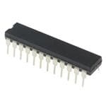
| 供应商器件封装 | 24-PDIP |
| 信噪比 | 137 dB |
| 分辨率 | 24 bit |
| 包装 | 管件 |
| 商标 | Analog Devices |
| 安装类型 | 通孔 |
| 安装风格 | Through Hole |
| 封装 | Tube |
| 封装/外壳 | 24-DIP(0.300",7.62mm) |
| 封装/箱体 | PDIP-24 |
| 工作温度 | -40°C ~ 105°C |
| 工作电源电压 | 5 V |
| 工厂包装数量 | 15 |
| 接口类型 | Serial (3-Wire, SPI, QSPI, Microwire) |
| 数据接口 | DSP,MICROWIRE™,QSPI™,串行,SPI™ |
| 最大功率耗散 | 7 mW |
| 最大工作温度 | + 105 C |
| 最小工作温度 | - 40 C |
| 标准包装 | 15 |
| 特性 | PGA |
| 电压参考 | Internal, External |
| 电压源 | 模拟和数字 |
| 系列 | AD7714 |
| 结构 | Sigma-Delta |
| 转换器数 | 1 |
| 转换器数量 | 1 |
| 转换速率 | 1 kS/s |
| 输入数和类型 | 3 个差分,单极3 个差分,双极5 个伪差分,单极5 个伪差分,双极 |
| 输入类型 | Differential |
| 通道数量 | 5 Channel |
| 配用 | /product-detail/zh/EVAL-AD7714-3EBZ/EVAL-AD7714-3EBZ-ND/1551308 |
| 采样率(每秒) | 1k |


PDF Datasheet 数据手册内容提取
a m 3 V/5 V, CMOS, 500 A Signal Conditioning ADC AD7714 FEATURES FUNCTIONAL BLOCK DIAGRAM Charge Balancing ADC 24 Bits No Missing Codes AVDD DVDD REF IN(–) REF IN(+) 0.0015% Nonlinearity AVDD CHARGE Five-Channel Programmable Gain Front End BALANCING Gains from 1 to 128 1mA A/D CONVERTER CInapnu tBse o Cro Fnivfieg uPrseedu daos -TDhifrfeeer eFnutlilayl DInifpfuertesntial AAAIIINNN123 HINGRIX MODUS L-DATOR SSYTANNCDBY Three-Wire Serial Interface AAIINN45 WITCMAT BUFFER PGA DIGITAL FILTER SPI™, QSPI™, MICROWIRE™ and DSP Compatible AIN6 S A = 1–128 3 V (AD7714-3) or 5 V (AD7714-5) Operation 1mA SERIAL INTERFACE Low Noise (<150nV rms) AGND REGISTER BANK SCLK Low Current (350␣mA typ) with Power-Down (5 mA typ) BUFFER CS AD7714Y Grade: MCLK IN CLOCK DIN +2.7 V to 3.3 V or +4.75 V to +5.25 V Operation MCLK OUT GENERATION DOUT 0.0010% Linearity Error AD7714 –408C to +1058C Temperature Range Schmitt Trigger on SCLK and DIN AGND DGND POL DRDY RESET Low Current (226␣mA typ) with Power-Down (4 mA typ) for three-wire operation. Gain settings, signal polarity and channel Lower Power Dissipation than Standard AD7714 selection can be configured in software using the serial port. The Available in 24-Lead TSSOP Package AD7714 provides self-calibration, system calibration and back- Low-Pass Filter with Programmable Filter Cutoffs ground calibration options and also allows the user to read and Ability to Read/Write Calibration Coefficients write the on-chip calibration registers. APPLICATIONS CMOS construction ensures very low power dissipation, and the Portable Industrial Instruments power-down mode reduces the standby power consumption to Portable Weigh Scales 15␣m W typ. The part is available in a 24-pin, 0.3 inch-wide, plastic Loop-Powered Systems dual-in-line package (DIP); a 24-lead small outline (SOIC) Pressure Transducers package, a 28-lead shrink small outline package (SSOP) and a 24-lead thin shrink small outline package (TSSOP). GENERAL DESCRIPTION† The AD7714 is a complete analog front end for low-frequency PRODUCT HIGHLIGHTS measurement applications. The device accepts low level signals 1. The AD7714Y offers the following features in addition to the directly from a transducer and outputs a serial digital word. It standard AD7714: wider temperature range, Schmitt trigger employs a sigma-delta conversion technique to realize up to 24 on SCLK and DIN, operation down to 2.7 V, lower power bits of no missing codes performance. The input signal is applied consumption, better linearity, and availability in 24-lead to a proprietary programmable gain front end based around an TSSOP package. analog modulator. The modulator output is processed by an on- 2. The AD7714 consumes less than 500 m A (f = 1␣MHz) CLK IN chip digital filter. The first notch of this digital filter can be or 1 mA (f = 2.5␣MHz) in total supply current, making CLK IN programmed via the on-chip control register allowing adjust- it ideal for use in loop-powered systems. ment of the filter cutoff and settling time. 3. The programmable gain channels allow the AD7714 to ac- The part features three differential analog inputs (which can also cept input signals directly from a strain gage or transducer be configured as five pseudo-differential analog inputs) as well as a removing a considerable amount of signal conditioning. differential reference input. It operates from a single supply (+3␣V 4. The AD7714 is ideal for microcontroller or DSP processor or +5␣V). The AD7714 thus performs all signal conditioning and applications with a three-wire serial interface reducing the num- conversion for a system consisting of up to five channels. ber of interconnect lines and reducing the number of opto- The AD7714 is ideal for use in smart, microcontroller- or DSP- couplers required in isolated systems. The part contains based systems. It features a serial interface that can be configured on-chip registers that allow control over filter cutoff, input gain, channel selection, signal polarity and calibration modes. †See page 39 for data sheet index. 5. The part features excellent static performance specifications SPI and QSPI are trademarks of Motorola, Inc. with 24-bit no missing codes, – 0.0015% accuracy and low MICROWIRE is a trademark of National Semiconductor Corporation. rms noise (140 nV). Endpoint errors and the effects of tem- REV. C perature drift are eliminated by on-chip self-calibration, Information furnished by Analog Devices is believed to be accurate and which removes zero-scale and full-scale errors. reliable. However, no responsibility is assumed by Analog Devices for its use, nor for any infringements of patents or other rights of third parties One Technology Way, P.O. Box 9106, Norwood, MA 02062-9106, U.S.A. which may result from its use. No license is granted by implication or Tel: 781/329-4700 World Wide Web Site: http://www.analog.com otherwise under any patent or patent rights of Analog Devices. Fax: 781/326-8703 © Analog Devices, Inc., 1998
AD7714-5–SPECIFICATIONS (AV = +5␣V, DV = +3.3␣V or +5␣V, REF IN(+) = +2.5␣V; REF␣IN(–) = AGND; DD DD f = 2.4576␣MHz unless otherwise noted. All specifications T to T unless otherwise noted.) CLK IN MIN MAX Parameter A Versions1 Units Conditions/Comments STATIC PERFORMANCE No Missing Codes 24 Bits min Guaranteed by Design. Bipolar Mode. For Filter Notches £ 60 Hz 22 Bits min For Filter Notch = 100 Hz 18 Bits min For Filter Notch = 250 Hz 15 Bits min For Filter Notch = 500 Hz 12 Bits min For Filter Notch = 1 kHz Output Noise See Tables I to IV Depends on Filter Cutoffs and Selected Gain Integral Nonlinearity – 0.0015 % of FSR max Filter Notches £ 60 Hz Unipolar Offset Error See Note 2 Unipolar Offset Drift3 0.5 m V/(cid:176)C typ For Gains of 1, 2, 4 0.3 m V/(cid:176)C typ For Gains of 8, 16, 32, 64, 128 Bipolar Zero Error See Note 2 Bipolar Zero Drift3 0.5 m V/(cid:176)C typ For Gains of 1, 2, 4 0.3 m V/(cid:176)C typ For Gains of 8, 16, 32, 64, 128 Positive Full-Scale Error4 See Note 2 Full-Scale Drift3, 5 0.5 m V/(cid:176)C typ For Gains of 1, 2, 4 0.3 m V/(cid:176)C typ For Gains of 8, 16, 32, 64, 128 Gain Error6 See Note 2 Gain Drift3, 7 0.5 ppm of FSR/(cid:176)C typ Bipolar Negative Full-Scale Error – 0.0015 % of FSR max Typically – 0.0004% Bipolar Negative Full-Scale Drift3 1 m V/(cid:176)C typ For Gains of 1, 2, 4 0.6 m V/(cid:176)C typ For Gains of 8, 16, 32, 64, 128 ANALOG INPUTS/REFERENCE INPUTS Specifications for AIN and REF IN Unless Noted Input Common-Mode Rejection (CMR) 90 dB min At DC. Typically 102 dB Normal-Mode 50 Hz Rejection8 100 dB min For Filter Notches of 10 Hz, 25 Hz, 50 Hz, – 0.02 · f NOTCH Normal-Mode 60 Hz Rejection8 100 dB min For Filter Notches of 10 Hz, 30 Hz, 60 Hz, – 0.02 · f NOTCH Common-Mode 50 Hz Rejection8 150 dB min For Filter Notches of 10 Hz, 25 Hz, 50 Hz, – 0.02 · f NOTCH Common-Mode 60 Hz Rejection8 150 dB min For Filter Notches of 10 Hz, 30 Hz, 60 Hz, – 0.02 · f NOTCH Common-Mode Voltage Range9 AGND to AV V min to V max AIN for BUFFER = 0 and REF IN DD Absolute AIN/REF IN Voltage9 AGND – 30 mV V min AIN for BUFFER = 0 and REF IN AV + 30 mV V max DD Absolute/Common-Mode AIN Voltage9 AGND + 50 mV V min BUFFER = 1. A Version AV – 1.5V V max DD AIN Input Current8 1 nA max A Version AIN Sampling Capacitance8 7 pF max AIN Differential Voltage Range10 0 to +V /GAIN11 nom Unipolar Input Range (B/U Bit of Filter High Register = 1) REF – V /GAIN nom Bipolar Input Range (B/U Bit of Filter High Register = 0) REF AIN Input Sampling Rate, f GAIN · f /64 For Gains of 1, 2, 4 S CLK␣IN f /8 For Gains of 8, 16, 32, 64, 128 CLK␣IN REF IN(+) – REF IN(–) Voltage +2.5 V nom – 1% for Specified Performance. Functional with Lower V REF REF IN Input Sampling Rate, f f /64 S CLK IN LOGIC INPUTS Input Current – 10 m A max All Inputs Except MCLK IN V , Input Low Voltage 0.8 V max DV = +5 V INL DD V , Input Low Voltage 0.4 V max DV = +3.3␣V INL DD V , Input High Voltage 2.4 V min DV = +5 V INH DD V , Input High Voltage 2.0 V min DV = +3.3 V INH DD MCLK IN Only V , Input Low Voltage 0.8 V max DV = +5␣V INL DD V , Input Low Voltage 0.4 V max DV = +3.3␣V INL DD V , Input High Voltage 3.5 V min DV = +5␣V INH DD V , Input High Voltage 2.5 V min DV = +3.3␣V INH DD LOGIC OUTPUTS (Including MCLK OUT) V , Output Low Voltage 0.4 V max I = 800␣m A Except for MCLK OUT.12 DV = +5 V OL SINK DD V , Output Low Voltage 0.4 V max I = 100␣m A Except for MCLK OUT.12 DV = +3.3 V OL SINK DD V , Output High Voltage 4.0 V min I = 200 m A Except for MCLK OUT.12 DV = +5␣V OH SOURCE DD V , Output High Voltage DV – 0.6V V min I = 100 m A Except for MCLK OUT.12 DV = +3.3␣V OH DD SOURCE DD Floating State Leakage Current – 10 m A max Floating State Output Capacitance13 9 pF typ Data Output Coding Binary Unipolar Mode Offset Binary Bipolar Mode NOTES 1Temperature range is as follows: A Versions: –40(cid:176)C to +85(cid:176)C. 2A calibration is effectively a conversion so these errors will be of the order of the conversion noise shown in Tables I to IV. This applies after calibration at the temperature of interest. 3Recalibration at any temperature will remove these drift errors. 4Positive Full-Scale Error includes Zero-Scale Errors (Unipolar Offset Error or Bipolar Zero Error) and applies to both unipolar and bipolar input ranges. 5Full-Scale Drift includes Zero-Scale Drift (Unipolar Offset Drift or Bipolar Zero Drift) and applies to both unipolar and bipolar input ranges. 6Gain Error does not include Zero-Scale Errors. It is calculated as Full-Scale Error—Unipolar Offset Error for unipolar ranges and Full-Scale Error—Bipolar Zero Error for bipolar ranges. –2– REV. C
AD7714 AD7714-3–SPECIFICATIONS (AV = +3.3␣V, DV = +3.3␣V, REF IN(+) = +1.25␣V; REF␣IN(–) = AGND; DD DD f = 2.4576␣MHz unless otherwise noted. All specifications T to T unless otherwise noted.) CLK IN MIN MAX Parameter A Versions Units Conditions/Comments STATIC PERFORMANCE No Missing Codes 24 Bits min Guaranteed by Design. Bipolar Mode. For Filter Notches £ 60 Hz 22 Bits min For Filter Notch = 100 Hz 18 Bits min For Filter Notch = 250 Hz 15 Bits min For Filter Notch = 500 Hz 12 Bits min For Filter Notch = 1 kHz Output Noise See Tables I to IV Depends on Filter Cutoffs and Selected Gain Integral Nonlinearity – 0.0015 % of FSR max Filter Notches £ 60 Hz Unipolar Offset Error See Note 2 Unipolar Offset Drift3 0.4 m V/(cid:176)C typ For Gains of 1, 2, 4 0.1 m V/(cid:176)C typ For Gains of 8, 16, 32, 64, 128 Bipolar Zero Error See Note 2 Bipolar Zero Drift3 0.4 m V/(cid:176)C typ For Gains of 1, 2, 4 0.1 m V/(cid:176)C typ For Gains of 8, 16, 32, 64, 128 Positive Full-Scale Error4 See Note 2 Full-Scale Drift3, 5 0.4 m V/(cid:176)C typ For Gains of 1, 2, 4 0.1 m V/(cid:176)C typ For Gains of 8, 16, 32, 64, 128 Gain Error6 See Note 2 Gain Drift3, 7 0.2 ppm of FSR/(cid:176)C typ Bipolar Negative Full-Scale Error – 0.003 % of FSR max Typically – 0.0004% Bipolar Negative Full-Scale Drift3 1 m V/(cid:176)C typ For Gains of 1, 2, 4 0.6 m V/(cid:176)C typ For Gains of 8, 16, 32, 64, 128 ANALOG INPUTS/REFERENCE INPUTS Specifications for AIN and REF IN Unless Noted Input Common-Mode Rejection (CMR) 90 dB min At DC. Typically 102 dB. Normal-Mode 50 Hz Rejection8 100 dB min For Filter Notches of 10 Hz, 25 Hz, 50 Hz, – 0.02 · f NOTCH Normal-Mode 60 Hz Rejection8 100 dB min For Filter Notches of 10 Hz, 30 Hz, 60 Hz, – 0.02 · f NOTCH Common-Mode 50 Hz Rejection8 150 dB min For Filter Notches of 10 Hz, 25 Hz, 50 Hz, – 0.02 · f NOTCH Common-Mode 60 Hz Rejection8 150 dB min For Filter Notches of 10 Hz, 30 Hz, 60 Hz, – 0.02 · f NOTCH Common-Mode Voltage Range9 AGND to AV V min to V max AIN for BUFFER = 0 and REF IN DD Absolute AIN/REF IN Voltage9 AGND – 30 mV V min AIN for BUFFER = 0 and REF IN AV + 30 mV V max DD Absolute/Common-Mode AIN Voltage9 AGND + 50 mV V min BUFFER = 1 AV – 1.5 V V max DD AIN Input Current8 1 nA max AIN Sampling Capacitance8 7 pF max AIN Differential Voltage Range10 0 to +V /GAIN11 nom Unipolar Input Range (B/U Bit of Filter High Register = 1) REF – V /GAIN nom Bipolar Input Range (B/U Bit of Filter High Register = 0) REF AIN Input Sampling Rate, f GAIN · f /64 For Gains of 1, 2, 4 S CLK␣IN f /8 For Gains of 8, 16, 32, 64, 128 CLK␣IN REF IN(+) – REF IN(–) Voltage +1.25 V nom – 1% for Specified Performance. Part Functions with Lower V REF REF IN Input Sampling Rate, f f /64 S CLK IN LOGIC INPUTS Input Current – 10 m A max All Inputs Except MCLK IN V , Input Low Voltage 0.4 V max INL V , Input High Voltage 2.0 V min INH MCLK IN Only V , Input Low Voltage 0.4 V max INL V , Input High Voltage 2.5 V min INH LOGIC OUTPUTS (Including MCLK OUT) V , Output Low Voltage 0.4 V max I = 100␣m A Except for MCLK OUT12 OL SINK V , Output High Voltage DV – 0.6 V min I = 100 m A Except for MCLK OUT12 OH DD SOURCE Floating State Leakage Current – 10 m A max Floating State Output Capacitance13 9 pF typ Data Output Coding Binary Unipolar Mode Offset Binary Bipolar Mode NOTES 7Gain Error Drift does not include Unipolar Offset Drift/Bipolar Zero Drift. It is effectively the drift of the part if zero-scale calibrations only were performed as is the case with background calibration. 8These numbers are guaranteed by design and/or characterization. 9The common-mode voltage range on the input pairs applies provided the absolute input voltage specification is obeyed. 10The input voltage range on the analog inputs is given here with respect to the voltage on the respective negative input of its differential or pseudo-differential pair. See Table VII for which inputs form differential pairs. 11VREF = REF IN(+) – REF IN(–). 12These logic output levels apply to the MCLK OUT output only when it is loaded with a single CMOS load. 13Sample tested at +25(cid:176)C to ensure compliance. 14See Burnout Current section. REV. C –3–
AD7714–SPECIFICATIONS (AV = + 3.3␣V to +5␣V, DV = +3.3␣V to +5␣V, REF IN(+) = +1.25␣V (AD7714-3) or +2.5␣V DD DD (AD7714-5); REF␣IN(–) = AGND; MCLK␣IN = 1␣MHz to 2.4576␣MHz unless otherwise noted. All specifications T to T unless otherwise noted.) MIN MAX Parameter A Versions Units Conditions/Comments TRANSDUCER BURNOUT14 Current 1 m A nom Initial Tolerance – 10 % typ Drift 0.1 %/(cid:176)C typ SYSTEM CALIBRATION Positive Full-Scale Calibration Limit15 (1.05 · V )/GAIN V max GAIN Is the Selected PGA Gain (Between 1 and 128) REF Negative Full-Scale Calibration Limit15 –(1.05 · V )/GAIN V max GAIN Is the Selected PGA Gain (Between 1 and 128) REF Offset Calibration Limit16 –(1.05 · V )/GAIN V max GAIN Is the Selected PGA Gain (Between 1 and 128) REF Input Span16 0.8 · V /GAIN V min GAIN Is the Selected PGA Gain (Between 1 and 128) REF (2.1 · V )/GAIN V max GAIN Is the Selected PGA Gain (Between 1 and 128) REF POWER REQUIREMENTS Power Supply Voltages AV Voltage (AD7714-3) +3 to +3.6 V For Specified Performance DD AV Voltage (AD7714-5) +4.75 to +5.25 V For Specified Performance DD DV Voltage +3 to +5.25 V For Specified Performance DD Power Supply Currents AV Current AV = 3.3␣V or 5␣V. BST Bit of Filter High Register = 017 DD DD 0.27 mA max Typically 0.2 mA. BUFFER = 0 V. f = 1␣MHz or 2.4576␣MHz CLK IN 0.6 mA max Typically 0.4 mA. BUFFER = DV . f = 1␣MHz or 2.4576␣MHz DD CLK IN AV = 3.3␣V or 5␣V. BST Bit of Filter High Register = 117 DD 0.5 mA max Typically 0.3␣mA. BUFFER = 0␣V. f = 2.4576␣MHz CLK IN 1.1 mA max Typically 0.8␣mA. BUFFER = DV . f = 2.4576␣MHz DD CLK IN DV Current18 Digital I/Ps = 0␣V or DV External MCLK IN DD DD. 0.23 mA max Typically 0.15␣mA. DV = 3.3␣V. f = 1␣MHz DD CLK IN 0.4 mA max Typically 0.3␣mA. DV = 5␣V. f = 1␣MHz DD CLK IN 0.5 mA max Typically 0.4␣mA. DV = 3.3␣V. f = 2.4576␣MHz DD CLK IN 0.8 mA max Typically 0.6␣mA. DV = 5␣V. f = 2.4576␣MHz DD CLK IN Power Supply Rejection19 See Note 20 dB typ Normal-Mode Power Dissipation18 AV = DV = +3.3␣V. Digital I/Ps = 0␣V or DV . External MCLK IN DD DD DD 1.65 mW max Typically 1.25␣mW. BUFFER = 0␣V. f = 1␣MHz. BST Bit = 0 CLK IN 2.75 mW max Typically 1.8␣mW. BUFFER = +3.3␣V. f = 1␣MHz. BST Bit = 0 CLK IN 2.55 mW max Typically 2␣mW. BUFFER = 0␣V. f = 2.4576␣MHz. BST Bit = 0 CLK IN 3.65 mW max Typically 2.6␣mW. BUFFER = +3.3␣V. f = 2.4576␣MHz. BST Bit = 0 CLK IN Normal-Mode Power Dissipation AV = DV = +5␣V. Digital I/Ps = 0␣V or DV . External MCLK IN DD DD DD 3.35 mW max Typically 2.5␣mW. BUFFER = 0␣V. f = 1␣MHz. BST Bit = 0 CLK IN 5 mW max Typically 3.5␣mW. BUFFER = +5␣V. f = 1␣MHz. BST Bit = 0 CLK IN 5.35 mW max Typically 4␣mW. BUFFER = 0␣V. f = 2.4576␣MHz. BST Bit = 0 CLK IN 7 mW max Typically 5␣mW. BUFFER = +5␣V. f = 2.4576␣MHz. BST Bit = 0 CLK IN Standby (Power-Down) Current21 40 m A max External MCLK IN = 0 V or DV . Typically 20␣m A. V = +5 V DD DD Standby (Power-Down) Current21 10 m A max External MCLK IN = 0 V or DV . Typically 5␣m A. V = +3.3 V DD DD NOTES 15After calibration, if the input voltage exceeds positive full scale, the converter will output all 1s. If the input is less than negative full scale, then the device outputs all 0s. 16These calibration and span limits apply provided the absolute voltage on the analog inputs does not exceed AVDD + 30␣mV or go more negative than AGND␣–␣30␣mV. The offset calibration limit applies to both the unipolar zero point and the bipolar zero point. 17For higher gains (‡ 8) at fCLK␣IN = 2.4576␣MHz, the BST bit of the Filter High Register must be set to 1. For other conditions, it can be set to 0. 18When using a crystal or ceramic resonator across the MCLK pins as the clock source for the device, the DVDD current and power dissipation will vary depending on the crystal or resonator type (see Clocking and Oscillator Circuit section). 19Measured at dc and applies in the selected passband. PSRR at 50 Hz will exceed 120 dB with filter notches of 5 Hz, 10 Hz, 25 Hz or 50 Hz. PSRR at 60 Hz will exceed 120dB with filter notches of 6 Hz, 10 Hz, 30 Hz or 60 Hz. 20PSRR depends on gain. For Gain of 1 : 70 dB typ: For Gain of 2 : 75 dB typ; For Gain of 4 : 80 dB typ; For Gains of 8 to 128 : 85 dB typ. 21If the external master clock continues to run in standby mode, the standby current increases to 150 m A typical with 5 V supplies and 75 m A typical with 3.3 V supplies. When using a crystal or ceramic resonator across the MCLK pins as the clock source for the device, the internal oscillator continues to run in standby mode and the power dissipation depends on the crystal or resonator type (see Standby Mode section). Specifications subject to change without notice. –4– REV. C
AD7714 AD7714Y–SPECIFICATIONS (AV = DV = +2.7␣V to +3.3␣V or 4.75 V to 5.25 V, REF IN(+) = +1.25␣V; with AV = 3 V DD DD DD and +2.5 V with AV = 5 V; REF␣IN(–) = AGND; MCLK IN = 2.4576␣MHz unless otherwise noted. All specifications T to T unless otherwise noted.) DD MIN MAX Parameter Y Versions1 Units Conditions/Comments STATIC PERFORMANCE No Missing Codes 24 Bits min Guaranteed by Design. For Filter Notches £ 60 Hz 22 Bits min For Filter Notch = 100 Hz 18 Bits min For Filter Notch = 250 Hz 15 Bits min For Filter Notch = 500 Hz 12 Bits min For Filter Notch = 1 kHz Output Noise See Tables I to IV Depends on Filter Cutoffs and Selected Gain Integral Nonlinearity – 0.001 % of FSR max Filter Notches £ 60 Hz. Unipolar Offset Error See Note 2 Unipolar Offset Drift3 0.4 m V/(cid:176) C typ For Gains of 1, 2, 4 0.1 m V/(cid:176)C typ For Gains of 8, 16, 32, 64, 128 Bipolar Zero Error See Note 2 Bipolar Zero Drift3 0.4 m V/(cid:176) C typ For Gains of 1, 2, 4 0.1 m V/(cid:176)C typ For Gains of 8, 16, 32, 64, 128 Positive Full-Scale Error4 See Note 2 Full-Scale Drift3, 5 0.4 m V/(cid:176) C typ For Gains of 1, 2, 4 0.1 m V/(cid:176)C typ For Gains of 8, 16, 32, 64, 128 Gain Error6 See Note 2 Gain Drift3, 7 0.2 ppm of FSR/ (cid:176)C typ Bipolar Negative Full-Scale Error2 – 0.0015 % of FSR max AV = 5 V. Typically – 0.0004% DD – 0.003 % of FSR max AV = 3 V. Typically – 0.0004% DD Bipolar Negative Full-Scale Drift3 1 m V/(cid:176) C typ For Gains of 1 to 4 0.6 m V/(cid:176) C typ For Gains of 8 to 128 ANALOG INPUTS/REFERENCE INPUTS Specifications for AIN and REF IN Unless Noted Input Common-Mode Rejection (CMR)8 90 dB min At DC. Typically 102 dB. Normal-Mode 50 Hz Rejection8 100 dB min For Filter Notches of 10 Hz, 25 Hz, 50 Hz, – 0.02 · f NOTCH Normal-Mode 60 Hz Rejection8 100 dB min For Filter Notches of 10 Hz, 30 Hz, 60 Hz, – 0.02 · f NOTCH Common-Mode 50 Hz Rejection8 150 dB min For Filter Notches of 10 Hz, 25 Hz, 50 Hz, – 0.02 · f NOTCH Common-Mode 60 Hz Rejection8 150 dB min For Filter Notches of 10 Hz, 30 Hz, 60 Hz, – 0.02 · f NOTCH Absolute/Common-Mode REF IN Voltage8 AGND to AV V min to V max DD Absolute/Common-Mode AIN Voltage8, 9 AGND – 30 mV V min BUF Bit of Setup Register = 0 AV + 30 mV V max DD Absolute/Common-Mode AIN Voltage8, 9 AGND + 50 mV V min BUF Bit of Setup Register = 1 AV – 1.5 V V max DD AIN DC Input Current8 1 nA max AIN Sampling Capacitance8 7 pF max AIN Differential Voltage Range10 0 to +V /GAIN11 nom Unipolar Input Range (B/U Bit of Filter High Register = 1) REF – V /GAIN nom Bipolar Input Range (B/U Bit of Filter High Register = 0) REF AIN Input Sampling Rate, f GAIN · f /64 For Gains of 1 to 4 S CLK␣IN f /8 For Gains of 8 to 128 CLK␣IN Reference Input Range REF IN(+) – REF IN(–) Voltage 1/1.75 V min/max AV = 2.7 V to 3.3 V. V = 1.25 – 1% for Specified Performance DD REF REF IN(+) – REF IN(–) Voltage 1/3.5 V min/max AV = 4.75 V to 5.25 V. V = 2.5 – 1% for Specified Performance DD REF REF IN Input Sampling Rate, f f /64 S CLK IN LOGIC INPUTS Input Current – 10 m A max All Inputs Except MCLK IN V , Input Low Voltage 0.8 V max DV = 5 V INL DD 0.4 V max DV = 3 V DD V , Input High Voltage 2.4 V min DV = 5 V INH DD 2 V min DV = 3 V DD SCLK & DIN Only (Schmitt Triggered Input) DV = 5 V NOMINAL DD V 1.4/3 V min/V max T+ V 0.8/1.4 V min/V max T– V – V 0.4/0.8 V min/V max T+ T– SCLK & DIN Only (Schmitt Triggered Input) DV = 3 V NOMINAL DD V 1/2.5 V min/V max T+ V 0.4/1.1 V min/V max T– V – V 0.375/0.8 V min/V max T+ T– MCLK In Only DV = 5 V NOMINAL DD V , Input Low Voltage 0.8 V max INL V , Input High Voltage 3.5 V min INH MCLK In Only DV = 3 V NOMINAL DD V , Input Low Voltage 0.4 V max INL V , Input High Voltage 2.5 V min INH LOGIC OUTPUTS (Including MCLK OUT) V , Output Low Voltage 0.4 V max I = 800␣m A with DV = 5 V. Except for MCLK OUT12 OL SINK DD V , Output Low Voltage 0.4 V max I = 100␣m A with DV = 3 V. Except for MCLK OUT12 OL SINK DD V , Output High Voltage 4 V min I = 200 m A with DV = 5 V. Except for MCLK OUT12 OH SOURCE DD REV. C –5–
AD7714Y Parameter Y Versions Units Conditions/Comments LOGIC OUTPUTS (Continued)) V , Output High Voltage DV – 0.6 V min I = 100 m A with DV = 3 V. Except for MCLK OUT12 OH DD SOURCE DD Floating State Leakage Current – 10 m A max Floating State Output Capacitance13 9 pF typ Data Output Coding Binary Unipolar Mode Offset Binary Bipolar Mode TRANSDUCER BURNOUT14 Current 1 m A nom Initial Tolerance – 10 % typ Drift 0.1 %/(cid:176)C typ SYSTEM CALIBRATION Positive Full-Scale Calibration Limit15 (1.05 · V )/GAIN V max GAIN Is the Selected PGA Gain (Between 1 and 128) REF Negative Full-Scale Calibration Limit15 –(1.05 · V )/GAIN V max GAIN Is the Selected PGA Gain (Between 1 and 128) REF Offset Calibration Limit16 –(1.05 · V )/GAIN V max GAIN Is the Selected PGA Gain (Between 1 and 128) REF Input Span16 0.8 · V /GAIN V min GAIN Is the Selected PGA Gain (Between 1 and 128) REF (2.1 · V )/GAIN V max GAIN Is the Selected PGA Gain (Between 1 and 128) REF POWER REQUIREMENTS Power Supply Voltages AV Voltage +2.7 to +3.3 or V DD +4.75 to +5.25 V For Specified Performance DV Voltage +2.7 to +5.25 V For Specified Performance DD Power Supply Currents AV Current AV = 3 V or 5␣V. BST Bit of Filter High Register = 017, CLKDIS = 1 DD DD 0.28 mA max Typically 0.22 mA. BUFFER = 0 V. f = 1␣MHz or 2.4576␣MHz CLK IN 0.6 mA max Typically 0.45 mA. BUFFER = DV . f = 1␣MHz or 2.4576␣MHz DD CLK IN AV = 3 V or 5␣V. BST Bit of Filter High Register = 117 DD 0.5 mA max Typically 0.38␣mA. BUFFER = 0␣V. f = 2.4576␣MHz CLK IN 1.1 mA max Typically 0.8␣mA. BUFFER = DV . f = 2.4576␣MHz DD CLK IN DV Current18 Digital I/Ps = 0␣V or DV External MCLK IN, CLKDIS = 1 DD DD. 0.080 mA max Typically 0.06␣mA. DV = 3 V. f = 1␣MHz DD CLK IN 0.16 mA max Typically 0.13␣mA. DV = 5␣V. f = 1␣MHz DD CLK IN 0.18 mA max Typically 0.15␣mA. DV = 3 V. f = 2.4576␣MHz DD CLK IN 0.35 mA max Typically 0.3 mA. DV = 5␣V. f = 2.4576␣MHz DD CLK IN Power Supply Rejection19 See Note 20 dB typ Normal-Mode Power Dissipation18 AV = DV = +3 V. Digital I/Ps = 0␣V or DV . External MCLK IN DD DD DD BST Bit of Filter High Register = 017 1.05 mW max Typically 0.84␣mW. BUFFER = 0␣V. f = 1␣MHz. BST Bit = 0 CLK IN 2.04 mW max Typically 1.53␣mW. BUFFER = +3 V. f = 1␣MHz. BST Bit = 0 CLK IN 1.35 mW max Typically 1.11␣mW. BUFFER = 0␣V. f = 2.4576␣MHz. BST Bit = 0 CLK IN 2.34 mW max Typically 1.9␣mW. BUFFER = +3 V. f = 2.4576␣MHz. BST Bit = 0 CLK IN Normal-Mode Power Dissipation AV = DV = +5␣V. Digital I/Ps = 0␣V or DV . External MCLK IN DD DD DD 2.1 mW max Typically 1.75 mW. BUFFER = 0␣V. f = 1␣MHz. BST Bit = 0 CLK IN 3.75 mW max Typically 2.9 mW. BUFFER = +5␣V. f = 1␣MHz. BST Bit = 0 CLK IN 3.1 mW max Typically 2.6␣mW. BUFFER = 0␣V. f = 2.4576␣MHz. BST Bit = 0 CLK IN 4.75 mW max Typically 3.75␣mW. BUFFER = +5␣V. f = 2.4576␣MHz. BST Bit = 0 CLK IN Standby (Power-Down) Current21 18 m A max External MCLK IN = 0 V or DV . Typically 9␣m A. V = +5 V DD DD Standby (Power-Down) Current21 10 m A max External MCLK IN = 0 V or DV . Typically 4␣m A. V = +3 V DD DD NOTES 1Temperature range is as follows: Y Version: –40(cid:176)C to +105(cid:176)C. 2A calibration is effectively a conversion so these errors will be of the order of the conversion noise shown in Tables I to IV. This applies after calibration at the temperature of interest. 3Recalibration at any temperature will remove these drift errors. 4Positive Full-Scale Error includes Zero-Scale Errors (Unipolar Offset Error or Bipolar Zero Error) and applies to both unipolar and bipolar input ranges. 5Full-Scale Drift includes Zero-Scale Drift (Unipolar Offset Drift or Bipolar Zero Drift) and applies to both unipolar and bipolar input ranges. 6Gain Error does not include Zero-Scale Errors. It is calculated as Full-Scale Error—Unipolar Offset Error for unipolar ranges and Full-Scale Error—Bipolar Zero Error for bipolar ranges. 7Gain Error Drift does not include Unipolar Offset Drift/Bipolar Zero Drift. It is effectively the drift of the part if zero-scale calibrations only were performed as is the case with background calibration. 8These numbers are guaranteed by design and/or characterization. 9The common-mode voltage range on the input pairs applies provided the absolute input voltage specification is obeyed. 10The input voltage range on the analog inputs is given here with respect to the voltage on the respective negative input of its differential or pseudo-differential pair. See Table VII for which inputs form differential pairs. 11VREF = REF IN(+) – REF IN(–). 12These logic output levels apply to the MCLK OUT output only when it is loaded with a single CMOS load. 13Sample tested at +25(cid:176)C to ensure compliance. 14See Burnout Current section. 15After calibration, if the input voltage exceeds positive full scale, the converter will output all 1s. If the input is less than negative full scale, then the device outputs all 0s. 16These calibration and span limits apply provided the absolute voltage on the analog inputs does not exceed AVDD + 30␣mV or go more negative than AGND␣–␣30␣mV. The offset calibration limit applies to both the unipolar zero point and the bipolar zero point. 17For higher gains (‡ 8) at fCLK␣IN = 2.4576␣MHz, the BST bit of the Filter High Register must be set to 1. For other conditions, it can be set to 0. 18When using a crystal or ceramic resonator across the MCLK pins as the clock source for the device, the DVDD current and power dissipation will vary depending on the crystal or resonator type (see Clocking and Oscillator Circuit section). 19Measured at dc and applies in the selected passband. PSRR at 50 Hz will exceed 120 dB with filter notches of 5 Hz, 10 Hz, 25 Hz or 50 Hz. PSRR at 60 Hz will exceed 120dB with filter notches of 6 Hz, 10 Hz, 30 Hz or 60 Hz. 20PSRR depends on gain. Gain 1 2 4 8–128 AVDD = 3 V 86 dB 78 dB 85 dB 93 dB AVDD = 5 V 90 dB 78 dB 84 dB 91 dB 21If the external master clock continues to run in standby mode, the standby current increases to 150 m A typical with 5 V supplies and 75 m A typical with 3.3 V supplies. When using a crystal or ceramic resonator across the MCLK pins as the clock source for the device, the internal oscillator continues to run in standby mode and the power dissipation depends on the crystal or resonator type (see Standby Mode section). Specifications subject to change without notice. –6– REV. C
AD7714 (AV = DV = +2.7 V to +5.25 V; AGND = DGND = 0 V; f = 2.5␣MHz; Input Logic 0 = 0 V, TIMING CHARACTERISTICS1, 2 DD DD CLKIN Logic 1 = DV unless otherwise noted.) DD Limit at T , T MIN MAX Parameter (A, Y Versions) Units Conditions/Comments f 3, 4 400 kHz min Master Clock Frequency: Crystal/Resonator or Externally CLKIN Supplied 2.5 MHz max For Specified Performance 2 t 0.4 · t ns min Master Clock Input Low Time. t = 1/f CLK IN LO CLK IN CLK IN CLK IN t 0.4 · t ns min Master Clock Input High Time CLK IN HI CLK IN t 500 · t ns nom DRDY High Time DRDY CLK IN t 100 ns min SYNC Pulsewidth 1 t 100 ns min RESET Pulsewidth 2 Read Operation t 0 ns min DRDY to CS Setup Time 3 t 0 ns min CS Falling Edge to SCLK Active Edge Setup Time5 4 t 6 0 ns min SCLK Active Edge to Data Valid Delay5 5 80 ns max DV = +5␣V DD 100 ns max DV = +3␣V DD t 100 ns min SCLK High Pulsewidth 6 t 100 ns min SCLK Low Pulsewidth 7 t 0 ns min CS Rising Edge to SCLK Active Edge Hold Time5 8 t 7 10 ns min Bus Relinquish Time after SCLK Active Edge5 9 60 ns max DV = +5␣V DD 100 ns max DV = +3␣V DD t 100 ns max SCLK Active Edge to DRDY High5, 8 10 Write Operation t 0 ns min CS Falling Edge to SCLK Active Edge Setup Time5 11 t 30 ns min Data Valid to SCLK Edge Setup Time 12 t 20 ns min Data Valid to SCLK Edge Hold Time 13 t 100 ns min SCLK High Pulsewidth 14 t 100 ns min SCLK Low Pulsewidth 15 t 0 ns min CS Rising Edge to SCLK Edge Hold Time 16 NOTES 1Sample tested at +25(cid:176)C to ensure compliance. All input signals are specified with tr = tf = 5 ns (10% to 90% of DV ) and timed from a voltage level of 1.6 V. DD 2See Figures 6 and 7. Timing applies for all grades. 3CLKIN Duty Cycle range is 45% to 55%. CLKIN must be supplied whenever the AD7714 is not in standby mode. If no clock is present in this case, the device can draw higher current than specified and possibly become uncalibrated. 4The AD7714 is production tested with f at 2.4576␣MHz (1␣MHz for some I tests). It is guaranteed by characterization to operate at 400␣kHz. CLKIN DD 5SCLK active edge is falling edge of SCLK with POL = 1; SCLK active edge is rising edge of SCLK with POL = 0. 6These numbers are measured with the load circuit of Figure 1 and defined as the time required for the output to cross the V or V limits. OL OH 7These numbers are derived from the measured time taken by the data output to change 0.5␣V when loaded with the circuit of Figure 1. The measured number is then extrapolated back to remove effects of charging or discharging the 100 pF capacitor. This means that the times quoted in the timing characteristics are the true bus relinquish times of the part and as such are independent of external bus loading capacitances. 8DRDY returns high after the first read from the device after an output update. The same data can be read again, if required, while DRDY is high although care should be taken that subsequent reads do not occur close to the next output update. Specifications subject to change without notice. ORDERING GUIDE AV Temperature Package DD Model Supply Range Option* AD7714AN-5 5 V –40(cid:176) C to +85(cid:176) C N-24 ISINK (800mA AT DVDD = +5V AD7714AR-5 5 V –40(cid:176) C to +85(cid:176) C R-24 100mA AT DVDD = +3.3V) AD7714ARS-5 5 V –40(cid:176) C to +85(cid:176) C RS-28 AD7714AN-3 3 V –40(cid:176) C to +85(cid:176) C N-24 TO OUTPUT +1.6V AD7714AR-3 3 V –40(cid:176) C to +85(cid:176) C R-24 PIN AD7714ARS-3 3 V –40(cid:176) C to +85(cid:176) C RS-28 50pF AD7714YN 3 V/5 V –40(cid:176) C to +105(cid:176) C N-24 AD7714YR 3 V/5 V –40(cid:176) C to +105(cid:176) C R-24 ISOURCE (200mA AT DVDD = +5V AD7714YRU 3 V/5 V –40(cid:176) C to +105(cid:176) C RU-24 100mA AT DVDD = +3.3V) AD7714AChips-5 5 V –40(cid:176) C to +85(cid:176) C Die AD7714AChips-3 3 V –40(cid:176) C to +85(cid:176) C Die Figure 1.Load Circuit for Access Time and Bus EVAL-AD7714-5EB 5V Evaluation Board Relinquish Time EVAL-AD7714-3EB 3V Evaluation Board *N = Plastic DIP; R = SOIC; RS = SSOP; RU = Thin Shrink Small Outline. REV. C –7–
AD7714 ABSOLUTE MAXIMUM RATINGS* SOIC Package, Power Dissipation . . . . . . . . . . . . . . . .450 mW (TA = +25(cid:176)C unless otherwise noted) q Thermal Impedance . . . . . . . . . . . . . . . . . . . . . . 75(cid:176) C/W JA AVDD to AGND . . . . . . . . . . . . . . . . . . . . . . . . –0.3 V to +7 V Lead Temperature, Soldering AV to DGND . . . . . . . . . . . . . . . . . . . . . . . . –0.3␣V to +7␣V Vapor Phase (60 sec) . . . . . . . . . . . . . . . . . . . . . . +215(cid:176) C DD DV to AGND . . . . . . . . . . . . . . . . . . . . . . . . –0.3␣V to +7␣V Infrared (15 sec) . . . . . . . . . . . . . . . . . . . . . . . . . . +220(cid:176) C DD DV to DGND . . . . . . . . . . . . . . . . . . . . . . . . –0.3␣V to +7␣V SSOP Package, Power Dissipation . . . . . . . . . . . . . . . .450 mW DD Analog Input Voltage to AGND . . . . . –0.3 V to AV + 0.3␣V q Thermal Impedance . . . . . . . . . . . . . . . . . . . . . 109(cid:176) C/W DD JA Reference Input Voltage to AGND . . . –0.3 V to AV + 0.3␣V Lead Temperature, Soldering DD Digital Input Voltage to DGND . . . . . –0.3 V to DV + 0.3 V Vapor Phase (60 sec) . . . . . . . . . . . . . . . . . . . . . . +215(cid:176) C DD Digital Output Voltage to DGND . . . . –0.3 V to DV + 0.3 V Infrared (15 sec) . . . . . . . . . . . . . . . . . . . . . . . . . . +220(cid:176) C DD Operating Temperature Range TSSOP Package, Power Dissipation . . . . . . . . . . . . . .450 mW Commercial (A Version) . . . . . . . . . . . . . . .–40(cid:176) C to +85(cid:176) C q Thermal Impedance . . . . . . . . . . . . . . . . . . . . . 128(cid:176) C/W JA Extended (Y Version) . . . . . . . . . . . . . . . . . –40(cid:176) C to +105(cid:176) C Lead Temperature, Soldering Storage Temperature Range . . . . . . . . . . . . . –65(cid:176) C to +150(cid:176) C Vapor Phase (60 sec) . . . . . . . . . . . . . . . . . . . . . . +215(cid:176) C Junction Temperature . . . . . . . . . . . . . . . . . . . . . . . . . .+150(cid:176) C Infrared (15 sec) . . . . . . . . . . . . . . . . . . . . . . . . . . +220(cid:176) C Plastic DIP Package, Power Dissipation . . . . . . . . . . . 450 mW *Stresses above those listed under Absolute Maximum Ratings may cause perma- q Thermal Impedance . . . . . . . . . . . . . . . . . . . . . 105(cid:176) C/W JA nent damage to the device. This is a stress rating only; functional operation of the Lead Temperature (Soldering, 10 sec) . . . . . . . . . . . .+260(cid:176) C device at these or any other conditions above those listed in the operational sections of this specification is not implied. Exposure to absolute maximum rating conditions for extended periods may affect device reliability. CAUTION ESD (electrostatic discharge) sensitive device. Electrostatic charges as high as 4000 V readily WARNING! accumulate on the human body and test equipment and can discharge without detection. Although these devices feature proprietary ESD protection circuitry, permanent damage may still occur on these devices if they are subjected to high energy electrostatic discharges. Therefore, ESD SENSITIVE DEVICE proper ESD precautions are recommended to avoid performance degradation or loss of functionality. PIN CONFIGURATIONS DIP and SOIC/TSSOP SSOP SCLK DGND SCLK DGND MCLK IN DVDD MCLK IN DVDD MCLK OUT DIN MCLK OUT DIN POL DOUT POL DOUT SYNC DRDY SYNC DRDY RESET CS AD7714 AD7714 RESET CS NC NC TOP VIEW TOP VIEW AIN1 (Not to Scale) AGND NC (Not to Scale) NC AIN2 AIN6 AIN1 AGND AIN3 AIN5 AIN2 AIN6 AIN4 REF IN(+) AIN3 AIN5 STANDBY REF IN(–) AIN4 REF IN(+) AVDD BUFFER STANDBY REF IN(–) AVDD BUFFER NC = NO CONNECT –8– REV. C
AD7714 PIN FUNCTION DESCRIPTION DIP/SOIC PIN NUMBERS Pin No. Mnemonic Function 1 SCLK Serial Clock. Logic Input. An external serial clock is applied to this input to access serial data from the AD7714. This serial clock can be a continuous clock with all data transmitted in a continuous train of pulses. 2 Alternatively, it can be a noncontinuous clock with the information being transmitted to the AD7714 in smaller batches of data. 2 MCLK IN Master Clock signal for the device. This can be provided in the form of a crystal/resonator or external clock. A crystal/resonator can be tied across the MCLK IN and MCLK OUT pins. Alternatively, the MCLK IN pin can be driven with a CMOS-compatible clock and MCLK OUT left unconnected. The part is specified with clock input frequencies of both 1 MHz and 2.4576 MHz. 3 MCLK OUT When the master clock for the device is a crystal/resonator, the crystal/resonator is connected between MCLK IN and MCLK␣OUT. If an external clock is applied to the MCLK IN, MCLK OUT provides an inverted clock signal. This clock can be used to provide a clock source for external circuits. 4 POL Clock Polarity. Logic Input. With this input low, the first transition of the serial clock in a data transfer operation is from a low to a high. In microcontroller applications, this means that the serial clock should idle low between data transfers. With this input high, the first transition of the serial clock in a data transfer operation is from a high to a low. In microcontroller applications, this means that the serial clock should idle high between data transfers. 5 SYNC Logic Input which allows for synchronization of the digital filters and analog modulators when using a number of AD7714s. While SYNC is low, the nodes of the digital filter, the filter control logic and the calibration control logic are reset and the analog modulator is also held in its reset state. SYNC does not affect the digital interface and does not reset DRDY if it is low. 6 RESET Logic Input. Active low input which resets the control logic, interface logic, digital filter and analog modulator of the part to power-on status. 7 AIN1 Analog Input Channel 1. Programmable-gain analog input which can be used as a pseudo-differential input when used with AIN6 or as the positive input of a differential analog input pair when used with AIN2 (see Communications Register section). 8 AIN2 Analog Input Channel 2. Programmable-gain analog input which can be used as a pseudo-differential input when used with AIN6 or as the negative input of a differential analog input pair when used with AIN1 (see Communications Register section). 9 AIN3 Analog Input Channel 3. Programmable-gain analog input which can be used as a pseudo-differential input when used with AIN6 or as the positive input of a differential analog input pair when used with AIN4 (see Communications Register section). 10 AIN4 Analog Input Channel 4. Programmable-gain analog input which can be used as a pseudo-differential input when used with AIN6 or as the negative input of a differential analog input pair when used with AIN3 (see Communications Register section). 11 STANDBY Logic Input. Taking this pin low shuts down the analog and digital circuitry, reducing current consumption to typically 5 m A. 12 AV Analog Positive Supply Voltage, A Grade Versions: +3.3␣V nominal (AD7714-3) or +5␣V nominal (AD7714-5); DD Y Grade Versions: 3 V or 5 V nominal. 13 BUFFER Buffer Option Select. Logic Input. With this input low, the on-chip buffer on the analog input (after the multiplexer and before the analog modulator) is shorted out. With the buffer shorted out the current flowing in the AV line is reduced to 270 m A. With this input high, the on-chip buffer is in series with the analog input DD allowing the inputs to handle higher source impedances. 14 REF IN(–) Reference Input. Negative input of the differential reference input to the AD7714. The REF IN(–) can lie anywhere between AV and AGND provided REF␣IN(+) is greater than REF IN(–). DD 15 REF IN(+) Reference Input. Positive input of the differential reference input to the AD7714. The reference input is differential with the provision that REF IN(+) must be greater than REF IN(–). REF IN(+) can lie anywhere between AV and AGND. DD 16 AIN5 Analog Input Channel 5. Programmable-gain analog input which is the positive input of a differential analog input pair when used with AIN6 (see Communications Register section). 17 AIN6 Analog Input Channel 6. Reference point for AIN1 through AIN4 in pseudo-differential mode or as the negative input of a differential input pair when used with AIN5 (see Communications Register section). 18 AGND Ground reference point for analog circuitry. REV. C –9–
AD7714 PIN FUNCTION DESCRIPTION (Continued) Pin No. Mnemonic Function 19 CS Chip Select. Active low Logic Input used to select the AD7714. With this input hard-wired low, the AD7714 can operate in its three-wire interface mode with SCLK, DIN and DOUT used to interface to the device. CS can be used to select the device in systems with more than one device on the serial bus or as a frame synchronization signal in communicating with the AD7714. 20 DRDY Logic output. A logic low on this output indicates that a new output word is available from the AD7714 data register. The DRDY pin will return high upon completion of a read operation of a full output word. If no data read has taken place, after an output update, the DRDY line will return high for 500 · t cycles prior to CLK␣IN the next output update. This gives an indication of when a read operation should not be attempted to avoid reading from the data register as it is being updated. DRDY is also used to indicate when the AD7714 has completed its on-chip calibration sequence. 21 DOUT Serial Data Output with serial data being read from the output shift register on the part. This output shift register can contain information from the calibration registers, mode register, communications register, filter selection registers or data register depending on the register selection bits of the Communications Register. 22 DIN Serial Data Input with serial data being written to the input shift register on the part. Data from this input shift register is transferred to the calibration registers, mode register, communications register or filter selection registers depending on the register selection bits of the Communications Register. 23 DV Digital Supply Voltage, A Grade Versions: +3.3␣V or +5 V nominal; Y Grade Versions: 3 V or 5 V nominal. DD 24 DGND Ground reference point for digital circuitry. TERMINOLOGY* BIPOLAR NEGATIVE FULL-SCALE ERROR INTEGRAL NONLINEARITY This is the deviation of the first code transition from the ideal This is the maximum deviation of any code from a straight line AIN(+) voltage (AIN(–) – VREF/GAIN + 0.5␣LSB) when operat- passingthroughtheendpointsofthetransferfunction. The end- ing in the bipolar mode. points of the transfer function are zero scale (not to be confused POSITIVE FULL-SCALE OVERRANGE withbipolarzero),apoint0.5LSBbelowthefirstcode transi- Positive Full-Scale Overrange is the amount of overhead avail- tion (000...000 to 000...001) and full scale, a point able to handle input voltages on AIN(+) input greater than 0.5LSB abovethelastcodetransition(111...110to AIN(–) + V /GAIN (for example, noise peaks or excess volt- REF 111...111). The error is expressed as a percentage of full ages due to system gain errors in system calibration routines) scale. without introducing errors due to overloading the analog modu- lator or overflowing the digital filter. POSITIVE FULL-SCALE ERROR Positive Full-Scale Error is the deviation of the last code transi- NEGATIVE FULL-SCALE OVERRANGE tion (111...110 to 111...111) from the ideal AIN(+) voltage This is the amount of overhead available to handle voltages on (AIN(–) + VREF/GAIN – 3/2 LSBs). It applies to both unipolar AIN(+) below AIN(–) – VREF/GAIN without overloading the and bipolar analog input ranges. analog modulator or overflowing the digital filter. Note that the analog input will accept negative voltage peaks even in the uni- UNIPOLAR OFFSET ERROR polar mode provided that AIN(+) is greater than AIN(–) and Unipolar Offset Error is the deviation of the first code transition greater than AGND – 30␣mV. from the ideal AIN(+) voltage (AIN(–) + 0.5 LSB) when oper- ating in the unipolar mode. OFFSET CALIBRATION RANGE In the system calibration modes, the AD7714 calibrates its BIPOLAR ZERO ERROR offset with respect to the analog input. The Offset Calibration This is the deviation of the midscale transition (0111...111 Range specification defines the range of voltages that the to 1000...000) fromtheidealAIN(+)voltage(AIN(–)– AD7714 can accept and still calibrate offset accurately. 0.5LSB) when operating in the bipolar mode. FULL-SCALE CALIBRATION RANGE GAIN ERROR This is the range of voltages that the AD7714 can accept in the This is a measure of the span error of the ADC. It includes full- system calibration mode and still calibrate full scale correctly. scale errors but not zero-scale errors. For unipolar input ranges it is defined as (full-scale error – unipolar offset error) while for INPUT SPAN bipolar input ranges it is defined as (full-scale error – bipolar In system calibration schemes, two voltages applied in sequence zero error). to the AD7714’s analog input define the analog input range. The input span specification defines the minimum and maxi- mum input voltages from zero to full scale that the AD7714 can accept and still calibrate gain accurately. *AIN(–) refers to the negative input of the differential input pairs or to AIN6 when referring to the pseudo-differential input configurations. –10– REV. C
AD7714 AD7714-5 OUTPUT NOISE Table Ia shows the output rms noise and effective resolution for some typical notch and –3␣dB frequencies for the AD7714-5 with f = 2.4576␣MHz while Table Ib gives the information for f = 1␣MHz. The numbers given are for the bipolar input ranges CLK␣IN CLK IN with a V of +2.5␣V and with BUFFER = 0. These numbers are typical and are generated at an analog input voltage of 0␣V. The REF numbers in brackets in each table are for the effective resolution of the part (rounded to the nearest 0.5␣LSB). The effective resolu- tion of the device is defined as the ratio of the output rms noise to the input full scale (i.e., 2 · V /GAIN). It should be noted that REF it is not calculated using peak-to-peak output noise numbers. Peak-to-peak noise numbers can be up to 6.6 times the rms numbers while effective resolution numbers based on peak-to-peak noise can be 2.5 bits below the effective resolution based on rms noise as 2 quoted in the tables. The output noise from the part comes from two sources. The first is the electrical noise in the semiconductor devices used in the implementation of the modulator (device noise). Secondly, when the analog input signal is converted into the digital domain, quan- tization noise is added. The device noise is at a low level and is largely independent of frequency. The quantization noise starts at an even lower level but rises rapidly with increasing frequency to become the dominant noise source. Consequently, lower filter notch settings (below 100␣Hz approximately for f = 2.4576␣MHz and below 40␣Hz approximately for f = 1␣MHz) tend to CLK IN CLK IN be device noise dominated while higher notch settings are dominated by quantization noise. Changing the filter notch and cutoff frequency in the quantization-noise dominated region results in a more dramatic improvement in noise performance than it does in the device-noise dominated region as shown in Table I. Furthermore, quantization noise is added after the PGA, so effective resolu- tion is largely independent of gain for the higher filter notch frequencies. Meanwhile, device noise is added in the PGA and, there- fore, effective resolution reduces at high gains for lower notch frequencies. Additionally, in the device-noise dominated region, the output noise (in m V) is largely independent of reference voltage while in the quantization-noise dominated region, the noise is pro- portional to the value of the reference. It is possible to do post-filtering on the device to improve the output data rate for a given –3␣dB frequency and also to further reduce the output noise. At the lower filter notch settings (below 60␣Hz for f = 2.4576␣MHz and below 25␣Hz for f = 1␣MHz), the no missing CLK IN CLK IN codes performance of the device is at the 24-bit level. At the higher settings, more codes will be missed until at 1␣kHz notch setting for f = 2.4576␣MHz (400␣Hz for f = 1␣MHz), no missing codes performance is only guaranteed to the 12-bit level. CLK␣IN CLK IN Table Ia. AD7714-5 Output Noise/Resolution vs. Gain and First Notch for f = 2.4576␣MHz, BUFFER = 0 CLK IN Filter First Typical Output RMS Noise in mV (Effective Resolution in Bits) Notch & O/P –3␣dB Gain of Gain of Gain of Gain of Gain of Gain of Gain of Gain of Data Rate Frequency 1 2 4 8 16 32 64 128 5␣Hz 1.31␣Hz 0.87 (22.5) 0.48 (22.5) 0.24 (22.5) 0.2 (21.5) 0.18 (20.5) 0.17 (20) 0.17 (19) 0.17 (18) 10␣Hz 2.62␣Hz 1.0 (22.5) 0.78 (21.5) 0.48 (21.5) 0.33 (21) 0.25 (20.5) 0.25 (19.5) 0.25 (18.5)0.25 (17.5) 25␣Hz 6.55␣Hz 1.8 (21.5) 1.1 (21) 0.63 (21) 0.5 (20) 0.44 (19.5) 0.41 (18.5) 0.38 (17.5)0.38 (16.5) 30␣Hz 7.86␣Hz 2.5 (21) 1.31 (21) 0.84 (20.5) 0.57 (20) 0.46 (19.5) 0.43 (18.5) 0.4 (17.5)0.4 (16.5) 50␣Hz 13.1␣Hz 4.33 (20) 2.06 (20) 1.2 (20) 0.64 (20) 0.54 (19) 0.46 (18.5) 0.46 (17.5)0.46 (16.5) 60␣Hz 15.72␣Hz 5.28 (20) 2.36 (20) 1.33 (20) 0.87 (19.5) 0.63 (19) 0.62 (18) 0.6 (17) 0.56 (16) 100␣Hz 26.2␣Hz 12.1 (18.5) 5.9 (18.5) 2.86 (19) 1.91 (18.5) 1.06 (18) 0.83 (17.5) 0.82 (16.5)0.76 (15.5) 250␣Hz 65.5␣Hz 127 (15.5) 58 (15.5) 29 (15.5) 15.9 (15.5) 6.7 (15.5) 3.72 (15.5) 1.96 (15.5)1.5 (14.5) 500␣Hz 131␣Hz 533 (13) 267 (13) 137 (13) 66 (13) 38 (13) 20 (13) 8.6 (13) 4.4 (13) 1␣kHz 262␣Hz 2,850 (11) 1,258 (11) 680 (11) 297 (11) 131 (11) 99 (10.5) 53 (10.5)28 (10.5) Table Ib. AD7714-5 Output Noise/Resolution vs. Gain and First Notch for f = 1␣MHz, BUFFER = 0 CLK IN Filter First Typical Output RMS Noise in mV (Effective Resolution in Bits) Notch & O/P –3␣dB Gain of Gain of Gain of Gain of Gain of Gain of Gain of Gain of Data Rate Frequency 1 2 4 8 16 32 64 128 2␣Hz 0.52␣Hz 0.75 (22.5) 0.56 (22) 0.31 (22) 0.19 (21.5) 0.17 (21) 0.14 (20) 0.14 (19) 0.14 (18) 4␣Hz 1.05␣Hz 1.04 (22) 0.88 (21.5) 0.45 (21.5) 0.28 (21) 0.21 (20.5) 0.21 (19.5) 0.21 (18.5)0.21 (17.5) 10␣Hz 2.62␣Hz 1.66 (21.5) 1.01 (21.5) 0.77 (20.5) 0.41 (20.5) 0.37 (19.5) 0.35 (19) 0.35 (18) 0.35 (17) 25 Hz 6.55␣Hz 5.2 (20) 2.06 (20) 1.4 (20) 0.86 (19.5) 0.63 (19) 0.61 (18) 0.59 (17) 0.59 (16) 30␣Hz 7.86␣Hz 7.1 (19.5) 3.28 (19.5) 1.42 (19.5) 1.07 (19) 0.78 (18.5) 0.64 (18) 0.61 (17) 0.61 (16) 50␣Hz 13.1␣Hz 19.4 (18) 9.11 (18) 4.2 (18) 2.45 (18) 1.56 (17.5) 1.1 (17) 0.82 (16.5)0.8 (15.5) 60␣Hz 15.72␣Hz 25 (17.5) 16 (17.5) 6.5 (17.5) 2.9 (17.5) 1.93 (17.5) 1.4 (17) 1.1 (16) 0.98 (15.5) 100␣Hz 26.2␣Hz 102 (15.5) 58 (15.5) 25 (15.5) 13.5 (15.5) 5.7 (15.5) 3.9 (15.5) 2.1 (15) 1.3 (15) 200␣Hz 52.4␣Hz 637 (13) 259 (13) 130 (13) 76 (13) 33 (13) 16 (13) 11 (13) 6 (12.5) 400␣Hz 104.8␣Hz 2,830 (11) 1,430 (11) 720 (11) 334 (11) 220 (10.5) 94 (10.5) 54 (10.5)25 (10.5) REV. C –11–
AD7714 AD7714-3 OUTPUT NOISE Table IIa shows the output rms noise and effective resolution for some typical notch and –3␣dB frequencies for the AD7714-3 with f = 2.4576␣MHz while Table IIb gives the information for f = 1␣MHz. The numbers given are for the bipolar input CLK␣IN CLK IN ranges with a V of +1.25␣V and BUFFER = 0. These numbers are typical and are generated at an analog input voltage of 0␣V. REF The numbers in brackets in each table are for the effective resolution of the part (rounded to the nearest 0.5␣LSB). The effective resolution of the device is defined as the ratio of the output rms noise to the input full scale (i.e., 2 · V /GAIN). It should be REF noted that it is not calculated using peak-to-peak output noise numbers. Peak-to-peak noise numbers can be up to 6.6 times the rms numbers while effective resolution numbers based on peak-to-peak noise can be 2.5 bits below the effective resolution based on rms noise as quoted in the tables. The output noise from the part comes from two sources. The first is the electrical noise in the semiconductor devices used in the implementation of the modulator (device noise). Secondly, when the analog input signal is converted into the digital domain, quan- tization noise is added. The device noise is at a low level and is largely independent of frequency. The quantization noise starts at an even lower level but rises rapidly with increasing frequency to become the dominant noise source. Consequently, lower filter notch settings (below 100␣Hz approximately for f = 2.4576␣MHz and below 40␣Hz approximately for f = 1␣MHz) tend to CLK IN CLK IN be device noise dominated while higher notch settings are dominated by quantization noise. Changing the filter notch and cutoff frequency in the quantization noise dominated region results in a more dramatic improvement in noise performance than it does in the device-noise dominated region as shown in Table II. Furthermore, quantization noise is added after the PGA, so effective reso- lution is largely independent of gain for the higher filter notch frequencies. Meanwhile, device noise is added in the PGA and, there- fore, effective resolution suffers a little at high gains for lower notch frequencies. Additionally, in the device-noise dominated region, the output noise (in m V) is largely independent of reference voltage while in the quantization-noise dominated region, the noise is proportional to the value of the reference. It is possible to do post-filtering on the device to improve the output data ratefor a given –3␣dB frequency and also to further reduce the output noise. At the lower filter notch settings (below 60␣Hz for f = 2.4576␣MHz and below 25␣Hz for f = 1␣MHz), the no missing CLK IN CLK IN codes performance of the device is at the 24-bit level. At the higher settings, more codes will be missed until at 1␣kHz notch setting for f = 2.4576␣MHz (400␣Hz for f = 1␣MHz), no missing codes performance is only guaranteed to the 12-bit level. CLK␣IN CLK IN Table IIa. AD7714-3 Output Noise/Resolution vs. Gain and First Notch for f = 2.4576␣MHz, BUFFER = 0 CLK IN Filter First Typical Output RMS Noise in mV (Effective Resolution in Bits) Notch & O/P –3␣dB Gain of Gain of Gain of Gain of Gain of Gain of Gain of Gain of Data Rate Frequency 1 2 4 8 16 32 64 128 5␣Hz 1.31␣Hz 1.07 (21) 0.68 (21) 0.29 (21) 0.24 (20) 0.22 (19.5) 0.22 (18.5) 0.22 (17.5)0.22 (16.5) 10␣Hz 2.62␣Hz 1.69 (20.5) 1.1 (20) 0.56 (20) 0.35 (19.5) 0.33 (19) 0.33 (18) 0.33 (17) 0.33 (16) 25␣Hz 6.55␣Hz 3.03 (19.5) 1.7 (19.5) 0.89 (19.5) 0.55 (19) 0.49 (18.5) 0.46 (17.5) 0.46 (16.5)0.45 (15.5) 30␣Hz 7.86␣Hz 3.55 (19.5) 2.1 (19) 1.1 (19) 0.61 (18.5) 0.58 (18) 0.57 (17) 0.55 (16) 0.55 (15) 50␣Hz 13.1␣Hz 4.72 (19) 2.3 (19) 1.5 (18.5) 0.84 (18.5) 0.7 (18) 0.68 (17) 0.67 (16) 0.66 (15) 60␣Hz 15.72␣Hz 5.12 (19) 3.1 (18.5) 1.6 (18) 0.98 (18) 0.9 (17.5) 0.7 (17) 0.69 (16) 0.68 (15) 100␣Hz 26.2␣Hz 9.68 (18) 5.6 (18) 2.4 (18) 1.3 (18) 1.1 (17) 0.95 (16.5) 0.88 (15.5)0.9 (14.5) 250␣Hz 65.5␣Hz 44 (16) 31 (15.5) 15 (15.5) 5.8 (15.5) 3.7 (15.5) 2.4 (15) 1.8 (14.5)1.8 (13.5) 500␣Hz 131␣Hz 304 (13) 129 (13) 76 (13) 33 (13) 20 (13) 11 (13) 6.3 (12.5)3 (12.5) 1␣kHz 262␣Hz 1410 (11) 715 (11) 350 (11) 177 (11) 101 (10.5) 51 (10.5) 31 (10.5)12 (10.5) Table IIb. AD7714-3 Output Noise/Resolution vs. Gain and First Notch for f = 1␣MHz, BUFFER = 0 CLK IN Filter First Typical Output RMS Noise in mV (Effective Resolution in Bits) Notch & O/P –3␣dB Gain of Gain of Gain of Gain of Gain of Gain of Gain of Gain of Data Rate Frequency 1 2 4 8 16 32 64 128 2␣Hz 0.52␣Hz 0.86 (21.5) 0.58 (21) 0.32 (21) 0.21 (20.5) 0.2 (19.5) 0.2 (18.5) 0.2 (17.5)0.2 (16.5) 4␣Hz 1.05␣Hz 1.26 (21) 0.74 (20.5) 0.44 (20.5) 0.35 (20) 0.3 (19) 0.3 (18) 0.3 (17) 0.3 (16) 10␣Hz 2.62␣Hz 1.68 (20.5) 1.33 (20) 0.73 (20) 0.5 (19) 0.49 (18.5) 0.49 (17.5) 0.48 (16.5)0.47 (15.5) 25␣Hz 6.55␣Hz 3.82 (19.5) 2.0 (19.5) 1.2 (19) 0.88 (18.5) 0.66 (18) 0.57 (17) 0.55 (16) 0.55 (15) 30␣Hz 7.86␣Hz 4.88 (19) 2.1 (19) 1.3 (19) 0.93 (18.5) 0.82 (17.5) 0.69 (17) 0.68 (16) 0.66 (15) 50␣Hz 13.1␣Hz 11 (18) 4.8 (18) 2.4 (18) 1.4 (18) 1.4 (17) 0.73 (16.5) 0.71 (15.5)0.7 (15) 60␣Hz 15.72␣Hz 14.7 (17.5) 7.5 (17.5) 3.8 (17.5) 2.6 (17) 1.5 (16.5) 0.95 (16.5) 0.88 (15) 0.9 (14.5) 100␣Hz 26.2␣Hz 61 (15.5) 30 (15.5) 12 (15.5) 6.1 (15.5) 2.9 (15.5) 2.4 (15) 1.8 (14.5)1.8 (13.5) 200␣Hz 52.4␣Hz 275 (13) 130 (13) 65 (13) 33 (13) 17 (13) 11 (13) 6.3 (12.5)3 (12.5) 400 Hz 104.8␣Hz 1435 (11) 720 (11) 362 (11) 175 (11) 110 (10.5) 51 (10.5) 31 (10.5)12 (10.5) –12– REV. C
AD7714 BUFFERED MODE NOISE Table III shows the typical output rms noise and effective resolution for some typical notch and –3␣dB frequencies for the AD7714- 5 with f = 2.4576␣MHz and BUFFER = +5 V. Table IV gives the information for the AD7714-3 again with f = 2.4576 CLK␣IN CLK IN MHz and BUFFER = +5␣V. The numbers given are for the bipolar input ranges and are generated with a differential analog input voltage of 0␣V. For the AD7714-5, the V voltage is +2.5␣V while for the AD7714 the V voltage is +1.25␣V. The numbers in REF REF brackets in each table are for the effective resolution of the part (rounded to the nearest 0.5 LSB). The effective resolution of the device is defined as the ratio of the output rms noise to the input full scale (i.e., 2 · V /GAIN). It should be noted that it is not REF calculated using peak-to-peak output noise numbers. Peak-to-peak noise numbers can be up to 6.6 times the rms numbers while 2 effective resolution numbers based on peak-to-peak noise can be 2.5 bits below the effective resolution based on rms noise as quoted in the tables. Table III. AD7714-5 Buffered Mode Output Noise/Resolution for f = 2.4576␣MHz CLK IN Filter First Typical Output RMS Noise in mV (Effective Resolution in Bits) Notch & O/P –3␣dB Gain of Gain of Gain of Gain of Gain of Gain of Gain of Gain of Data Rate Frequency 1 2 4 8 16 32 64 128 5␣Hz 1.31␣Hz 0.99 (22.5) 0.68 (22) 0.46 (21.5) 0.26 (21) 0.26 (20) 0.26 (19) 0.26 (18) 0.26 (17) 10␣Hz 2.62␣Hz 1.5 (21.5) 0.95 (21.5) 0.63 (21) 0.41 (20.5) 0.39 (19.5) 0.36 (18.5) 0.36 (17.5)0.36 (16.5) 25␣Hz 6.55␣Hz 2.5 (21) 1.7 (20.5) 0.88 (20.5) 0.75 (19.5) 0.57 (19) 0.57 (18) 0.57 (17) 0.56 (16) 30␣Hz 7.86␣Hz 2.9 (20.5) 1.8 (20.5) 1 (20) 0.87 (19.5) 0.75 (18.5) 0.72 (17.5) 0.72 (16.5)0.71 (15.5) 50␣Hz 13.1␣Hz 4.2 (20) 2.5 (20) 1.5 (19.5) 1.1 (19) 0.94 (18.5) 0.94 (17.5) 0.94 (16.5)0.87 (15.5) 60␣Hz 15.72␣Hz 6.1 (19.5) 2.9 (19.5) 2 (19.5) 1.2 (19) 1 (18.5) 0.97 (17.5) 0.95 (16.5)0.94 (15.5) 100␣Hz 26.2␣Hz 13.8 (18.5) 6.5 (18.5) 3.5 (18.5) 2.2 (18) 1.3 (18) 1.2 (17) 1.3 (16) 1.1 (15) 250␣Hz 65.5␣Hz 87 (16) 56 (15.5) 25 (15.5) 11 (15.5) 5.7 (15.5) 3.6 (15.5) 2.4 (15) 2.1 (14) 500␣Hz 131␣Hz 508 (13.5) 241 (13.5) 117 (13.5) 73 (13) 34 (13) 16 (13) 8.5 (13) 5.2 (13) 1␣kHz 262␣Hz 2860 (11) 1700 (10.5) 745 (10.5) 480 (10.5) 197 (10.5) 94 (10.5) 53 (10.5)23 (10.5) Table IV. AD7714-3 Buffered Mode Output Noise/Resolution for f = 2.4576␣MHz CLK IN Filter First Typical Output RMS Noise in mV (Effective Resolution in Bits) Notch & O/P –3␣dB Gain of Gain of Gain of Gain of Gain of Gain of Gain of Gain of Data Rate Frequency 1 2 4 8 16 32 64 128 5␣Hz 1.31␣Hz 1.16 (21) 0.76 (20.5) 0.34 (20) 0.29 (20) 0.29 (19) 0.28 (18) 0.26 (17) 0.26 (16) 10␣Hz 2.62␣Hz 1.7 (20.5) 1 (20.5) 0.7 (20) 0.46 (19.5) 0.45 (18.5) 0.4 (17.5) 0.4 (16.5)0.4 (15.5) 25␣Hz 6.55␣Hz 3.5 (19.5) 1.8 (19.5) 1.1 (19) 0.74 (18.5) 0.63 (18) 0.6 (17) 0.6 (16) 0.6 (15) 30␣Hz 7.86␣Hz 3.7 (19.5) 2.2 (19) 1.3 (19) 0.76 (18.5) 0.68 (18) 0.66 (17) 0.66 (16) 0.66 (15) 50␣Hz 13.1␣Hz 4.5 (19) 3 (18.5) 1.7 (18.5) 1.0 (18) 0.92 (17.5) 0.9 (16.5) 0.89 (15.5)0.89 (14.5) 60␣Hz 15.72␣Hz 5.3 (19) 3.3 (18.5) 1.8 (18.5) 1.1 (18) 1 (17) 0.96 (16.5) 0.96 (15.5)0.96 (14.5) 100␣Hz 26.2␣Hz 10 (18) 4.9 (18) 3.1 (17.5) 1.5 (17.5) 1.2 (17) 1.2 (16) 1.2 (15) 1.2 (14) 250␣Hz 65.5␣Hz 47 (15.5) 29 (15.5) 15 (15.5) 7.5 (15.5) 4.7 (15) 2.6 (15) 2.5 (14) 1.6 (13.5) 500␣Hz 131␣Hz 300 (13.5) 171 (13) 74 (13) 35 (13) 21 (13) 8.6 (13) 5.6 (13) 3.1 (12.5) 1␣kHz 262␣Hz 1722 (10.5) 735 (10.5) 380 (10.5) 230 (10.5) 93 (10.5) 55 (10.5) 30 (10.5)12 (10.5) REV. C –13–
AD7714 ON-CHIP REGISTERS The AD7714 contains eight on-chip registers which can be accessed via the serial port of the part. The first of these is a Communica- tions Register which controls the channel selection, decides whether the next operation is a read or write operation and also decides which register the next read or write operation accesses. All communications to the part must start with a write operation to the Communications Register. After power-on or RESET, the device expects a write to its Communications Register. The data written to this register determines whether the next operation to the part is a read or a write operation and also determines to which register this read or write operation occurs. Therefore, write access to any of the other registers on the part starts with a write operation to the Communications Register followed by a write to the selected register. A read operation from any other register on the part (including the output data register) starts with a write operation to the Communications Register followed by a read operation from the selected register. The communications register also controls channel selection and the DRDY status is also available by reading from the Communications Register. The second register is a Mode Register which determines calibration mode and gain setting. The third register is labelled the Filter High Register and this determines the word length, bipolar/unipolar operation and contains the upper 4 bits of the filter selection word. The fourth register is labelled the Filter Low Register and contains the lower 8 bits of the filter selec- tion word. The fifth register is a Test Register which is accessed when testing the device. The sixth register is the Data Register from which the output data from the part is accessed. The final registers allow access to the part’s calibration registers. The Zero Scale Calibration Register allows access to the zero scale calibration coefficients for the selected input channel while the Full Scale Calibra- tion Register allows access to the full scale calibration coefficients for the selected input channel. The registers are discussed in more detail in the following sections. Communications Register (RS2-RS0 = 0, 0, 0) The Communications Register is an 8-bit register from which data can either be read or to which data can be written. All communi- cations to the part must start with a write operation to the Communications Register. The data written to the Communications Reg- ister determines whether the next operation is a read or write operation and to which register this operation takes place. Once the subsequent read or write operation to the selected register is complete, the interface returns to where it expects a write operation to the Communications Register. This is the default state of the interface, and on power-up or after a RESET, the AD7714 is in this default state waiting for a write operation to the Communications Register. In situations where the interface sequence is lost, if a write operation of sufficient duration (containing at least 32 serial clock cycles) takes place with DIN high, the AD7714 returns to this default state. Table V outlines the bit designations for the Communications Register. Table V. Communications Register 0/DRDY RS2 RS1 RS0 R/W CH2 CH1 CH0 0/DRDY For a write operation, a 0 must be written to this bit so that the write operation to the Communications Register actually takes place. If a 1 is written to this bit, the part will not clock on to subsequent bits in the register. It will stay at this bit location until a 0 is written to this bit. Once a 0 is written to this bit, the next 7 bits will be loaded to the Communications Register. For a read operation, this bit provides the status of the DRDY flag from the part. The status of this bit is the same as the DRDY output pin. RS2–RS0 Register Selection Bits. RS2 is the MSB of the three selection bits. The three bits select to which one of eight on-chip registers the next read or write operation takes place as shown in Table VI along with the register size. Table VI. Register Selection RS2 RS1 RS0 Register Register Size 0 0 0 Communications Register 8 Bits 0 0 1 Mode Register 8 Bits 0 1 0 Filter High Register 8 Bits 0 1 1 Filter Low Register 8 Bits 1 0 0 Test Register 8 Bits 1 0 1 Data Register 16 Bits or 24 Bits 1 1 0 Zero-Scale Calibration Register 24 Bits 1 1 1 Full-Scale Calibration Register 24 Bits –14– REV. C
AD7714 CH2–CH0 Channel Select. These three bits select a channel either for conversion or for access to calibration coefficients as outlined in Table VII. There are three pairs of calibration registers on the part. In fully differential mode, the part has three input channels so each channel has its own pair of calibration registers. In pseudo-differential mode, the AD7714 has five input channels with some of the input channel combinations sharing calibration registers. With CH2, CH1 and CH0 at a logic 1, the part looks at the AIN6 input internally shorted to itself. This can be used as a test method to evaluate the noise performance of the part with no external noise sources. In this mode, the AIN6 input should be connected to an external voltage within the allowable common-mode range for the part. The Power-On or RESET status of these bits is 1,0,0 selecting the differential pair AIN1 and AIN2. 2 Table VII. Channel Selection CH2 CH1 CH0 AIN(+) AIN(–) Type Calibration Register Pair 0 0 0 AIN1 AIN6 Pseudo Differential Register Pair 0 0 0 1 AIN2 AIN6 Pseudo Differential Register Pair 1 0 1 0 AIN3 AIN6 Pseudo Differential Register Pair 2 0 1 1 AIN4 AIN6 Pseudo Differential Register Pair 2 1 0 0 AIN1 AIN2 Fully Differential Register Pair 0 1 0 1 AIN3 AIN4 Fully Differential Register Pair 1 1 1 0 AIN5 AIN6 Fully Differential Register Pair 2 1 1 1 AIN6 AIN6 Test Mode Register Pair 2 Mode Register (RS2-RS0 = 0, 0, 1); Power On/Reset Status: 00␣Hex The Mode Register is an eight bit register from which data can either be read or to which data can be written. Table VIII outlines the bit designations for the Mode Register. Table VIII. Mode Register MD2 MD1 MD0 G2 G1 G0 BO FSYNC MD2 MD1 MD0 Operating Mode 0 0 0 Normal Mode; this is the normal mode of operation of the device whereby the device is performing nor- mal conversions. This is the default condition of these bits after Power-On or RESET. 0 0 1 Self-Calibration; this activates self-calibration on the channel selected by CH2, CH1 and CH0 of the Communications Register. This is a one step calibration sequence and when complete the part returns to Normal Mode with MD2, MD1 and MD0 returning to 0, 0, 0. The DRDY output or bit goes high when calibration is initiated and returns low when this self-calibration is complete and a new valid word is available in the data register. The zero-scale calibration is performed at the selected gain on internally shorted (zeroed) inputs and the full-scale calibration is performed at the selected gain on an internally- generated V /Selected Gain. REF 0 1 0 Zero-Scale System Calibration; this activates zero scale system calibration on the channel selected by CH2, CH1 and CH0 of the Communications Register. Calibration is performed at the selected gain on the input voltage provided at the analog input during this calibration sequence. This input voltage should remain stable for the duration of the calibration. The DRDY output or bit goes high when calibration is initiated and returns low when this zero-scale calibration is complete and a new valid word is available in the data register. At the end of the calibration, the part returns to Normal Mode with MD2, MD1 and MD0 returning to 0, 0, 0. 0 1 1 Full-Scale System Calibration; this activates full-scale system calibration on the selected input channel. Calibration is performed at the selected gain on the input voltage provided at the analog input during this calibration sequence. This input voltage should remain stable for the duration of the calibration. Once again, the DRDY output or bit goes high when calibration is initiated and returns low when this full-scale calibration is complete and a new valid word is available in the data register. At the end of the calibration, the part returns to Normal Mode with MD2, MD1 and MD0 returning to 0, 0, 0. REV. C –15–
AD7714 MD2 MD1 MD0 Operating Mode (continued) 1 0 0 System-Offset Calibration; this activates system-offset calibration on the channel selected by CH2, CH1 and CH0 of the Communications Register. This is a one step calibration sequence and when complete the part returns to Normal Mode with MD2, MD1 and MD0 returning to 0, 0, 0. The DRDY output or bit goes high when calibration is initiated and returns low when this system offset calibration is com- plete and a new valid word is available in the data register. For this calibration type, the zero-scale cali- bration is performed at the selected gain on the input voltage provided at the analog input during this calibration sequence. This input voltage should remain stable for the duration of the calibration. The full-scale calibration is performed at the selected gain on an internally generated V /Selected Gain. REF 1 0 1 Background Calibration; this activates background calibration on the channel selected by CH2, CH1 and CH0 of the Communications Register. If the background calibration mode is on, then the AD7714 provides continuous self-calibration of the shorted (zeroed) inputs. This calibration takes place as part of the conversion sequence, extending the conversion time and reducing the word rate by a factor of six. Its major advantage is that the user does not have to worry about recalibrating the offset of the device when there is a change in the ambient temperature or supplies. In this mode, the zero-scale calibration is performed at the selected gain on internally shorted (zeroed) inputs. The calibrations are interleaved with normal conversions and the calibration registers of the device are automatically updated. Because the background calibration does not perform full-scale calibrations, a self-calibration should be per- formed before placing the part in the background calibration mode. 1 1 0 Zero-Scale Self-Calibration; this activates zero-scale self-calibration on the channel selected by CH2, CH1 and CH0 of the Communications Register. This zero-scale self-calibration is performed at the selected gain on internally shorted (zeroed) inputs. This is a one step calibration sequence and when complete the part returns to Normal Mode with MD2, MD1 and MD0 returning to 0, 0, 0. The DRDY output or bit goes high when calibration is initiated and returns low when this zero-scale self-calibration is complete and a new valid word is available in the data register. 1 1 1 Full-Scale Self-Calibration; this activates full-scale self-calibration on the channel selected by CH2, CH1 and CH0 of the Communications Register. This full-scale self-calibration is performed at the selected gain on an internally-generated V /Selected Gain. This is a one step calibration sequence and REF when complete the part returns to Normal Mode with MD2, MD1 and MD0 returning to 0, 0, 0. The DRDY output or bit goes high when calibration is initiated and returns low when this full-scale self- calibration is complete and a new valid word is available in the data register. G2 G1 G0 Gain Setting 0 0 0 1 0 0 1 2 0 1 0 4 0 1 1 8 1 0 0 16 1 0 1 32 1 1 0 64 1 1 1 128 BO Burnout Current. A 0 in this bit turns off the on-chip burnout currents. This is the default (Power-On or RESET) status of this bit. A 1 in this bit activates the burnout currents. When active, the burnout currents connect to the selected analog input pair, one to the AIN(+) input and one to the AIN(–) input. FSYNC Filter Synchronization. When this bit is high, the nodes of the digital filter, the filter control logic and the calibration control logic are held in a reset state and the analog modulator is also held in its reset state. When this bit goes low, the modulator and filter start to process data and a valid word is available in 3 · 1/(output update rate), i.e., the settling time of the filter. This FSYNC bit does not affect the digital interface and does not reset the DRDY output if it is low. –16– REV. C
AD7714 Filter Registers. Power On/Reset Status: Filter High Register: 01␣Hex. Filter Low Register: 40␣Hex. There are two 8-bit Filter Registers on the AD7714 from which data can either be read or to which data can be written. Tables IX and X outline the bit designations for the Filter Registers. Table IX. Filter High Register (RS2–RS0 = 0, 1, 0) B/U WL BST ZERO FS11 FS10 FS9 FS8 A Versions 2 B/U WL BST CLKDIS FS11 FS10 FS9 FS8 Y Versions Table X. Filter Low Register (RS2–RS0 = 0, 1, 1) FS7 FS6 FS5 FS4 FS3 FS2 FS1 FS0 All Versions B/U Bipolar/Unipolar Operation. A 0 in this bit selects Bipolar Operation. This is the default (Power-On or RESET) status of this bit. A 1 in this bit selects unipolar operation. WL Word Length. A 0 in this bit selects 16-bit word length when reading from the data register (i.e., DRDY returns high after 16 serial clock cycles in the read operation). This is the default (Power-On or RESET) status of this bit. A 1 in this bit selects 24-bit word length. BST Current Boost. A 0 in this bit reduces the current taken by the analog front end. When the part is operated with f = 1␣MHz or at gains of 1 to 4 with f = 2.4576␣MHz, this bit should be 0 to reduce the current CLK IN CLK IN drawn from AV , although the device will operate just as well with this bit at a 1. When the AD7714 is oper- DD ated at gains of 8 to 128 with f = 2.4576␣MHz, this bit must be 1 to ensure correct operation of the CLK IN device. The Power-On or RESET status of this bit is 0. ZERO To ensure correct operation of the A Versions of the part, a 0 must be written to this bit. CLKDIS Master Clock Disable Bit. A Logic 1 in this bit disables the master clock from appearing at the MCLKOUT pin. When disabled, the MCLKOUT pin is forced low. This feature allows the user the flexibility of using the MCLKOUT as a clock source for other devices in the system or for turning off the MCLKOUT as a power saving feature. When using an external master clock or the MCLKIN pin, the AD7714 continues to have inter- nal clocks and will convert normally with its CLKDIS bit active. When using a crystal oscillator or ceramic resonator across the MCLK IN or MCLKOUT pins, the AD7714 clock is stopped and no conversions take place when the CLKDIS bit is active. FS11–FS0 Filter Selection. The on-chip digital filter provides a Sinc3 (or (Sinx/x)3 ) filter response. The 12 bits of data programmed into these bits determine the filter cut-off frequency, the position of the first notch of the filter and the data rate for the part. In association with the gain selection, it also determines the output noise (and hence the effective resolution) of the device. The first notch of the filter occurs at a frequency determined by the relationship: filter first notch frequency =␣(f /128)/code CLK␣IN where code is the decimal equivalent of the code in bits FS0 to FS11 and is in the range 19 to 4,000. With the nominal f of 2.4576␣MHz, this results in a first notch frequency range from 4.8␣Hz to 1.01␣kHz. To CLK IN ensure correct operation of the AD7714, the value of the code loaded to these bits must be within this range. Failure to do this will result in unspecified operation of the device. Changing the filter notch frequency, as well as the selected gain, impacts resolution. Tables I through IV show the effect of the filter notch frequency and gain on the effective resolution of the AD7714. The output data rate (or effective conversion time) for the device is equal to the frequency selected for the first notch of the filter. For example, if the first notch of the filter is selected at 50␣Hz then a new word is available at a 50 Hz rate or every 20␣ms. If the first notch is at 1␣kHz, a new word is available every 1␣ms. The settling time of the filter to a full-scale step input change is worst case 4 · 1/(output data rate). For example, with the first filter notch at 50␣Hz, the settling time of the filter to a full-scale step input change is 80␣ms max. This settling time can be reduced to 3 · 1/(output data rate) by synchronizing the step input change to a reset of the digital filter. In other words, if the step input takes place with the SYNC input low or the FSYNC bit high, the settling time will be 3 · 1/(output data rate) from when SYNC returns high or FSYNC returns low. If a change of channel takes place, the settling time is 3 · 1/(output data rate) regardless of the SYNC or FSYNC status as the part issues an internal SYNC command when requested to change channels. The –3dB frequency is determined by the programmed first notch frequency according to the relationship: filter –3 dB frequency = 0.262 · filter first notch frequency. REV. C –17–
AD7714 Test Register (RS2–RS0 = 1, 0, 0) The part contains a Test Register which is used in testing the device. The user is advised not to change the status of any of the bits in this register from the default (Power-On or RESET) status of all 0s as the part will be placed in one of its test modes and will not operate cor- rectly. If the part enters one of its test modes, exercising RESET will exit the part from the mode. An alternative scheme for getting the part out of one of its test modes, is to reset the interface by writing 32 successive 1s to the part and then write all 0s to the Test Register. Data Register (RS2–RS0 = 1, 0, 1) The Data Register on the part is a read-only register which contains the most up-to-date conversion result from the AD7714. The register can be programmed to be either 16-bits or 24-bits wide, determined by the status of the WL bit of the Mode Register. If the Communications Register data sets up the part for a write operation to this register, a write operation must actually take place in order to return the part to where it is expecting a write operation to the Communications Register (the default state of the interface). However, the 16 or 24 bits of data written to the part will be ignored by the AD7714. Zero-Scale Calibration Register (RS2–RS0 = 1, 1, 0); Power On/Reset Status: 1F4000␣Hex The AD7714 contains three zero-scale calibration registers, labelled Zero-Scale Calibration Register 0 to Zero Scale Calibration Register␣2. The three registers are totally independent of each other such that in fully differential mode there is a zero-scale register for each of the input channels. Each of these registers is a 24-bit read/write register and, when writing to the registers, 24 bits must be written; otherwise no data will be transferred to the register. The register is used in conjunction with the associated full-scale calibra- tion register to form a register pair. These register pairs are associated with input channel pairs as outlined in Table VII. While the part is set up to allow access to these registers over the digital interface, the part itself no longer has access to the register coefficients to correctly scale the output data. As a result, there is a possibility that after accessing the calibration registers (either read or write operation) the first output data read from the part may contain incorrect data. In addition, a read or write operation to the calibration register should not be attempted while a calibration is in progress. These eventualities can be avoided by taking either the SYNC input low or the FSYNC bit of the Mode Register high before the calibration register operation and taking them either high or low respectively after the operation is complete. Full-Scale Calibration Register (RS2–RS0 = 1, 1, 1); Power On/Reset Status: 5761AB␣Hex The AD7714 contains three full-scale calibration registers, labelled Full-Scale Calibration Register 0 to Full-Scale Calibration Regis- ter 2. The three registers are totally independent of each other such that in fully differential mode there is a full-scale register for each of the input channels. Each of these registers is a 24-bit read/write register and, when writing to the registers, 24 bits must be written, otherwise no data will be transferred to the register. The register is used in conjunction with the associated zero-scale calibration register to form a register pair. These register pairs are associated with input channel pairs as outlined in Table␣VII. While the part is set up to allow access to these registers over the digital interface, the part itself no longer has access to the coeffi- cients to correctly scale the output data. As a result, there is a possibility that after accessing the calibration registers (either read or write operation) the first output data read from the part may contain incorrect data. In addition, a read or write operation to the calibration register should not be attempted while a calibration is in progress. These eventualities can be avoided by taking either the SYNC input low or the FSYNC bit of the Mode Register high before the calibration register operation and taking them either high or low respectively after the operation is complete. CALIBRATION OPERATIONS The AD7714 contains a number of calibration options as outlined previously. Table XI summarizes the calibration types, the opera- tions involved and the duration of the operations. There are two methods of determining the end of calibration. The first is to moni- tor when DRDY returns low at the end of the sequence. DRDY not only indicates when the sequence is complete but also that the part has a valid new sample in its data register. This valid new sample is the result of a normal conversion which follows the calibra- tion sequence. The second method of determining when calibration is complete is to monitor the MD2, MD1 and MD0 bits of the Mode Register. When these bits return to 0, 0, 0 following a calibration command, it indicates that the calibration sequence is com- plete. This method does not give any indication of there being a valid new result in the data register. However, it gives an earlier indication that calibration is complete than DRDY. The time to when the Mode Bits (MD2, MD1 and MD0) return to 0, 0, 0 represents the duration of the calibration. The sequence to when DRDY goes low also includes a normal conversion and a pipeline delay, t (2000 · t ), to correctly scale the results of this first conversion. The time for both methods is given in the table. P CLK IN Table XI. Calibration Operations Calibration Type MD2, MD1, MD0 Calibration Sequence Duration to Mode Bits Duration to DRDY Self Calibration 0, 0, 1 Internal ZS Cal @ Selected Gain + 6 · 1/Output Rate 9 · 1/Output Rate + t p Internal FS Cal @ Selected Gain ZS System Calibration 0, 1, 0 ZS Cal on AIN @ Selected Gain 3 · 1/Output Rate 4 · 1/Output Rate + t P FS System Calibration 0, 1, 1 FS Cal on AIN @ Selected Gain 3 · 1/Output Rate 4 · 1/Output Rate + t P System-Offset Calibration 1, 0, 0 ZS Cal on AIN @ Selected Gain + 6 · 1/Output Rate 9 · 1/Output Rate + t P Internal FS Cal @ Selected Gain Background Calibration 1, 0, 1 Internal ZS Cal @ Selected Gain + Bits Not Reset 6 · 1/Output Rate Normal Conversion ZS Self Calibration 1, 1, 0 Internal ZS Cal @ Selected Gain 3 · 1/Output Rate 6 · 1/Output Rate + t P FS Self Calibration 1, 1, 1 Internal FS Cal @ Selected Gain 3 · 1/Output Rate 6 · 1/Output Rate + t P –18– REV. C
AD7714 CIRCUIT DESCRIPTION modulator converts the sampled input signal into a digital pulse The AD7714 is a sigma-delta A/D converter with on-chip digi- train whose duty cycle contains the digital information. The tal filtering, intended for the measurement of wide dynamic programmable gain function on the analog input is also range, low frequency signals such as those in weigh-scale, pres- incorporated in this sigma-delta modulator with the input sam- sure transducer, industrial control or process control applica- pling frequency of the modulator being modified to give the tions. It contains a sigma-delta (or charge-balancing) ADC, a higher gains. A sinc3 digital low-pass filter processes the output calibration microcontroller with on-chip static RAM, a clock of the sigma-delta modulator and updates the output register at oscillator, a digital filter and a bidirectional serial communica- a rate determined by the first notch frequency of this filter. The 2 tions port. The part consumes only 500m A of power supply output data can be read from the serial port randomly or peri- current and features a standby mode which requires only 10m A, odically at any rate up to the output register update rate. The making it ideal for battery-powered or loop-powered instru- first notch of this digital filter, its –3␣dB frequency and its out- ments. The part comes in two versions, the AD7714-5, which is put rate can be programmed via the filter high and filter low specified for operation from a nominal +5␣V analog supply registers. With a master clock frequency of 2.4576MHz, the (AVDD), and the AD7714-3, which is specified for operation programmable range for this first notch frequency and output from a nominal +3.3␣V analog supply. Both versions can be rate is from 4.8␣Hz to 1.01kHz giving a programmable range operated with a digital supply (DVDD) voltage of either +3.3␣V for the –3␣dB frequency of 1.26Hz to 265␣Hz. or +5␣V. AD7714Y grade parts operate with a nominal AV DD The basic connection diagram for the part is shown in Figure 2. of 3 V or 5 V and can be operated with a digital supply voltage This shows both the AV and DV pins of the AD7714 being of either 3 V or 5 V. DD DD driven from the analog +3␣V or +5␣V supply. Some applications The part contains three programmable-gain fully differential will have AV and DV driven from separate supplies. In the DD DD analog input channels that can be reconfigured as five pseudo- connection diagram shown, the AD7714’s analog inputs are differential inputs. The gain range on all channels is from 1 to configured as three fully differential inputs. The part is set up 128, allowing the part to accept unipolar signals of between for unbuffered mode on the these analog inputs. An AD780, 0mV to +20␣mV and 0V to +2.5␣V. In bipolar mode, the part precision +2.5 V reference, provides the reference source for the handles genuine bipolar signals of – 20mV and quasi-bipolar part. On the digital side, the part is configured for three-wire signals up to – 2.5V when the reference input voltage equals operation with CS tied to DGND. A quartz crystal or ceramic +2.5␣V. With a reference voltage of +1.25␣V, the input ranges resonator provides the master clock source for the part. It may are from 0mV to +10mV to 0V to +1.25␣V in unipolar mode, be necessary to connect capacitors on the crystal or resonator to while in bipolar mode, the part handles genuine bipolar signals ensure that it does not oscillate at overtones of its fundamental of – 10mV and quasi-bipolar signals up to – 1.25V. operating frequency. The values of capacitors will vary depend- The part employs a sigma-delta conversion technique to realize ing on the manufacturer’s specifications. up to 24 bits of no missing codes performance. The sigma-delta ANALOG +5V SUPPLY 10mF 0.1mF 0.1mF AVDD DVDD ANDAILFOFEGR IENNPTUITA L1 AAIINN12 DRDY DRAEATADY CS DIFFERENTIAL AIN3 RECEIVE ANALOG INPUT 2 AIN4 DOUT (READ) DIFFERENTIAL AIN5 DIN SDEARTAIAL ANALOG INPUT 3 AIN6 SERIAL SCLK CLOCK AD7714 ANALOG ANALOG GROUND AGND RESET +5V +5V SUPPLY DIGITAL SYNC VIN GROUND DGND STANDBY VOUT REF IN(+) POL 10mF 0.1mF AD780 MCLK IN CRYSTAL OR GND REF IN(–) CERAMIC RESONATOR MCLK OUT BUFFER Figure 2.Basic Connection Diagram REV. C –19–
AD7714 ANALOG INPUT C must be charged through R and through any external SAMP SW Analog Input Ranges source impedances every input sample cycle. Therefore, in unbuf- The AD7714 contains six analog input pins (labelled AIN1 to fered mode, source impedances mean a longer charge time for AIN6) which can be configured as either three fully differential C and this may result in gain errors on the part. Table XII SAMP input channels or five pseudo-differential input channels. Bits shows the allowable external resistance/capacitance values, for CH0, CH1 and CH2 of the Communications Register configure unbuffered mode, such that no gain error to the 16-bit level is the analog input arrangement and the channel selection is as introduced on the part. Table XIII shows the allowable external outlined previously in Table VII. The input pairs (either differ- resistance/capacitance values, once again for unbuffered mode, ential or pseudo-differential) provide programmable-gain, input such that no gain error to the 20-bit level is introduced. channels which can handle either unipolar or bipolar input signals. It should be noted that the bipolar input signals are Table XII. External R, C Combination for No 16-Bit Gain referenced to the respective AIN(–) input of the input pair. Error (Unbuffered Mode Only) In unbuffered mode, the common-mode range of these inputs is Gain External Capacitance (pF) from AGND to AV provided that the absolute value of the analog DD input voltage lies between AGND␣–␣30␣mV and AV + 30␣mV. 0 50 100 500 1000 5000 DD This means that in unbuffered mode the part can handle both 1 368 kW 90.6 kW 54.2 kW 14.6 kW 8.2 kW 2.2 kW unipolar and bipolar input ranges for all gains. In buffered 2 177.2 kW 44.2 kW 26.4 kW 7.2 kW 4 kW 1.12 kW mode, the analog inputs can handle much larger source imped- 4 82.8 kW 21.2 kW 12.6 kW 3.4 kW 1.94 kW 540 W ances, but the absolute input voltage range is restricted to be- 8–128 35.2 kW 9.6 kW 5.8 kW 1.58 kW 880 W 240 W tween AGND␣+ 50␣mV to AV – 1.5␣V which also places DD restrictions on the common-mode range. This means that in buffered mode there are some restrictions on the allowable gains Table XIII. External R, C Combination for No 20-Bit Gain for bipolar input ranges. Care must be taken in setting up the Error (Unbuffered Mode Only) common-mode voltage and input voltage range so that the Gain External Capacitance (pF) above limits are not exceeded, otherwise there will be a degrada- tion in linearity performance. 0 50 100 500 1000 5000 In unbuffered mode, the analog inputs look directly into the 1 290 kW 69 kW 40.8 kW 10.4 kW 5.6 kW 1.4 kW 7␣pF input sampling capacitor, CSAMP. The dc input leakage 2 141 kW 33.8 kW 20 kW 5 kW 2.8 kW 700 W current in this unbuffered mode is 1␣nA maximum. As a result, 4 63.6 kW 16 kW 9.6 kW 2.4 kW 1.34 kW 340 W the analog inputs see a dynamic load which is switched at the 8–128 26.8 kW 7.2 kW 4.4 kW 1.1 kW 600 W 160 W input sample rate (see Figure 3). This sample rate depends on master clock frequency and selected gain. C is charged to In buffered mode, the analog inputs look into the high impedance SAMP AIN(+) and discharged to AIN(–) every input sample cycle. inputs stage of the on-chip buffer amplifier. C is charged via SAMP The effective on-resistance of the switch, R , is typically 7␣kW . this buffer amplifier such that source impedances do not affect SW the charging of C . This buffer amplifier has an offset leak- SAMP age current of 1␣nA. In this buffered mode, large source imped- ances result in a dc offset voltage developed across the source impedance but not in a gain error. AIN(+) RSW (7kV TYP) HIGH Input Sample Rate IMPEDANCE >1GV The modulator sample frequency for the AD7714 remains at AIN(–) CSAMP f /128 (19.2␣kHz @ f = 2.4576␣MHz) regardless of (7pF ) CLK␣IN CLK IN the selected gain. However, gains greater than 1 are achieved VBIAS by a combination of multiple input samples per modulator cycle SWITCHING FREQUENCY DEPENDS ON and a scaling of the ratio of reference capacitor to input capaci- fCLKIN AND SELECTED GAIN tor. As a result of the multiple sampling, the input sample rate of the device varies with the selected gain (see Table XIV). In Figure 3.Unbuffered Analog Input Structure buffered mode, the input is buffered before the input sampling capacitor. In unbuffered mode, where the analog input looks directly into the sampling capacitor, the effective input imped- ance is 1/C · f where C is the input sampling capaci- SAMP S SAMP tance and f is the input sample rate. S –20– REV. C
AD7714 Table XIV. Input Sampling Frequency vs. Gain for the AD7714-3. The part is functional with V voltages REF down to 1 V but with degraded performance as the output noise Gain Input Sampling Freq (fS) will, in terms of LSB size, be larger. REF␣IN(+) must always be 1 f /64 (38.4␣kHz @ f = 2.4576␣MHz) greater than REF␣IN(–) for correct operation of the AD7714. CLK IN CLK IN 2 2 · fCLK IN/64 (76.8␣kHz @ fCLK IN = 2.4576␣MHz) Both reference inputs provide a high impedance, dynamic load 4 4 · fCLK IN/64 (153.6␣kHz @ fCLK IN = 2.4576␣MHz) similar to the analog inputs in unbuffered mode. The maxi- 8 8 · fCLK IN/64 (307.2␣kHz @ fCLK IN = 2.4576␣MHz) mum dc input leakage current is – 1 nA over temperature and 16 8 · fCLK IN/64 (307.2␣kHz @ fCLK IN = 2.4576␣MHz) source resistance may result in gain errors on the part. In this 2 32 8 · fCLK IN/64 (307.2␣kHz @ fCLK IN = 2.4576␣MHz) case, the sampling switch resistance is 5␣kW typ and the refer- 64 8 · fCLK IN/64 (307.2␣kHz @ fCLK IN = 2.4576␣MHz) ence capacitor (CREF) varies with gain. The sample rate on the 128 8 · fCLK IN/64 (307.2␣kHz @ fCLK IN = 2.4576␣MHz) reference inputs is fCLK IN/64 and does not vary with gain. For gains of 1 to 8, C is 8pF; for a gain of 16, it is 5.5pF, for a REF Burnout Current gain of 32, it is 4.25pF, for a gain of 64, it is 3.625pF and for a The AD7714 contains two 1␣m A currents, one source current gain of 128, it is 3.3125pF. from AV to AIN(+) and one sink from AIN(–) to AGND. The DD The output noise performance outlined in Tables I through IV currents are either both on or off depending on the BO bit of the is for an analog input of 0V and is unaffected by noise on the Mode Register. These currents can be used in checking that a reference. To obtain the same noise performance as shown in transducer has not burned out nor gone open-circuit before the noise tables over the full input range requires a low noise attempting to take measurements on that channel. If the cur- reference source for the AD7714. If the reference noise in the rents are turned on, allowed flow in the transducer, a measure- bandwidth of interest is excessive, it will degrade the perfor- ment of the input voltage on the analog input taken and the mance of the AD7714. In applications where the excitation voltage measured is full scale, it indicates that the transducer has voltage for the bridge transducer on the analog input also de- gone open-circuit; if the voltage measured is zero, it indicates rives the reference voltage for the part, the effect of the noise in that the transducer has gone short-circuit. For normal opera- the excitation voltage will be removed as the application is tion, these burnout currents are turned off by writing a 0 to the ratiometric. Recommended reference voltage sources for the BO bit. For the source current to work correctly, the applied AD7714-5 and AD7714Y grade with AV = 5 V include the voltage on AIN(+) should not go within 500␣mV of AV . For DD DD AD780, REF43 and REF192 while the recommended reference the sink current to work correctly, the applied voltage on the sources for the AD7714-3 and AD7714Y with AV = 3 V AIN(–) input should not go within 500␣mV of AGND. DD include the AD589 and AD1580. It is generally recommended Bipolar/Unipolar Inputs to decouple the output of these references to further reduce the The analog inputs on the AD7714 can accept either unipolar or noise level. bipolar input voltage ranges. Bipolar input ranges do not imply that the part can handle negative voltages on its analog inputs, DIGITAL FILTERING since the analog input cannot go more negative than –30␣mV to The AD7714 contains an on-chip low-pass digital filter which ensure correct operation of the part. The input channels are processes the output of the part’s sigma-delta modulator. There- either fully differential or pseudo-differential (all other channels fore, the part not only provides the analog-to-digital conversion referenced to AIN6). In either case, the input channels are function but it also provides a level of filtering. There are a arranged in pairs with an AIN(+) and AIN(–). As a result, the number of system differences when the filtering function is voltage to which the unipolar and bipolar signals on the AIN(+) provided in the digital domain rather than the analog domain input are referenced is the voltage on the respective AIN(–) and the user should be aware of these. input. For example, if AIN(–) is +2.5␣V and the AD7714 is First, since digital filtering occurs after the A-to-D conversion configured for unipolar operation with a gain of 2 and a V of REF process, it can remove noise injected during the conversion +2.5␣V, the input voltage range on the AIN(+) input is +2.5V to process. Analog filtering cannot do this. Also, the digital filter +3.75␣V. If AIN(–) is +2.5␣V and the AD7714 is configured for can be made programmable far more readily than an analog bipolar mode with a gain of 2 and a V of +2.5␣V, the analog REF filter. Depending on the digital filter design, this gives the user input range on the AIN(+) input is +1.25␣V to +3.75 V (i.e., the capability of programming cutoff frequency and output 2.5␣V – 1.25␣V). If AIN(–) is at AGND, the part cannot be con- update rate. figured for bipolar ranges in excess of – 30␣mV. On the other hand, analog filtering can remove noise superim- Bipolar or unipolar options are chosen by programming the B/U posed on the analog signal before it reaches the ADC. Digital bit of the Filter High Register. This programs the selected chan- filtering cannot do this and noise peaks riding on signals near nel for either unipolar or bipolar operation. Programming the full scale have the potential to saturate the analog modulator channel for either unipolar or bipolar operation does not change and digital filter, even though the average value of the signal is any of the input signal conditioning; it simply changes the data within limits. To alleviate this problem, the AD7714 has over- output coding and the points on the transfer function where range headroom built into the sigma-delta modulator and digital calibrations occur. filter which allows overrange excursions of 5% above the analog input range. If noise signals are larger than this, consideration REFERENCE INPUT should be given to analog input filtering, or to reducing the The AD7714’s reference inputs, REF␣IN(+) and REF␣IN(–), input channel voltage so that its full scale is half that of the provide a differential reference input capability. The common- analog input channel full scale. This will provide an overrange mode range for these differential inputs is from AGND to AV . DD capability greater than 100% at the expense of reducing the The nominal reference voltage, V (REF␣IN(+)␣–REF␣IN(–)), REF dynamic range by 1 bit (50%). for specified operation is +2.5␣V for the AD7714-5 and +1.25␣V REV. C –21–
AD7714 In addition, the digital filter does not provide any rejection at The cutoff frequency of the digital filter is determined by the integer multiples of the digital filter’s sample frequency. How- value loaded to bits FS0 to FS11 in the Filter High and Filter ever, the input sampling on the part provides attenuation at Low Registers. Programming a different cutoff frequency via multiples of the digital filter’s sampling frequency so that the FS0 – FS11 does not alter the profile of the filter response; it unattenuated bands actually occur around multiples of the input changes the frequency of the notches as outlined in the Filter sampling frequency f (as defined in Table XIV). Thus, the Registers section. The output update and first notch correspond S unattenuated bands occur at n · f (where n = 1, 2, 3...). At and are determined by the relationship: S these frequencies, there are frequency bands, – f wide (f is 3 dB 3 dB Output Rate = f /(N.128) the cutoff frequency of the digital filter) at either side where CLK IN where N is the decimal equivalent of the word loaded to the noise passes unattenuated to the output. FS0 to FS11 bits of the Filter Registers Filter Characteristics The AD7714’s digital filter is a low-pass filter with a (sinx/x)3 while the –3␣dB frequency is determined by the relationship: response (also called sinc3). The transfer function for this filter –3␣dB frequency = 0.262 · filter first notch frequency is described in the z-domain by: The filter provides a linear phase response with a group delay determined by: H(z)=ØŒ 1 · 1- Z- N øœ 3 Group Delay = –3p.(N.f/fMOD ) ºŒ N 1- Z- 1 ßœ where N is the decimal equivalent of the word loaded to the FS0 to FS11 bits of the Filter Registers and f = f /128. and in the frequency domain by: MOD CLK IN Since the AD7714 contains this on-chip, low-pass filtering, a H(f)= 1 · Sin(N.p .f fS)3 settling time is associated with step function inputs and data on N Sin(p .f f ) the output will be invalid after a step change until the settling S time has elapsed. The settling time depends upon the output Figure 4 shows the filter frequency response for a cutoff rate chosen for the filter. The settling time of the filter to a full- frequency of 2.62␣Hz which corresponds to a first filter notch scale step input can be up to four times the output data period. frequency of 10␣Hz. The plot is shown from dc to 65␣Hz. For a synchronized step input (using the SYNC or FSYNC This response is repeated at either side of the input sampling functions) the settling time is three times the output data pe- frequency and at either side of multiples of the input sampling riod. When changing channels on the part, the change from one frequency. channel to the other is synchronized so the output settling time is also three times the output data period. Thus, in switching 0 between channels, the output data register is not updated until –20 the settling time of the filter has elapsed. –40 Post-Filtering –60 The on-chip modulator provides samples at a 19.2␣kHz output –80 rate with f at 2.4576␣MHz. The on-chip digital filter CLK IN dB–100 decimates these samples to provide data at an output rate that N – –120 corresponds to the programmed output rate of the filter. Since GAI–140 the output data rate is higher than the Nyquist criterion, the –160 output rate for a given bandwidth will satisfy most application –180 requirements. However, there may be some applications that –200 require a higher data rate for a given bandwidth and noise per- –220 formance. Applications that need this higher data rate will –240 require some post-filtering following the part’s digital filter. 0 10 20 30 40 50 60 FREQUENCY – Hz For example, if the required bandwidth is 7.86␣Hz but the required update rate is 100␣Hz, the data can be taken from the Figure 4.Frequency Response of AD7714 Filter AD7714 at the 100␣Hz rate giving a –3 dB bandwidth of The response of the filter is similar to that of an averaging filter 26.2␣Hz. Post-filtering can be applied to this to reduce the but with a sharper roll-off. The output rate for the digital filter bandwidth and output noise, to the 7.86␣Hz bandwidth level, corresponds with the positioning of the first notch of the filter’s while maintaining an output rate of 100␣Hz. frequency response. Thus, for the plot of Figure 4 where the Post-filtering can also be used to reduce the output noise from output rate is 10␣Hz, the first notch of the filter is at 10␣Hz. The notches of this (sinx/x)3 filter are repeated at multiples of the the device for bandwidths below 1.26␣Hz. At a gain of 128 and a bandwidth of 1.26␣Hz, the output rms noise is 140␣nV. This first notch. The filter provides attenuation of better than 100dB is essentially device noise or white noise and since the input is at these notches. For the example given, if the first notch is at chopped, the noise has a primarily flat frequency response. By 10␣Hz, there will be notches (and hence >100␣dB rejection) at reducing the bandwidth below 1.26␣Hz, the noise in the result- both 50␣Hz and 60␣Hz. ant passband can be reduced. A reduction in bandwidth by a factor of 2 results in a reduction of approximately 1.25 in the output rms noise. This additional filtering will result in a longer settling time. –22– REV. C
AD7714 ANALOG FILTERING value which, when normalized, is subtracted from all conversion The digital filter does not provide any rejection at integer mul- results. The full-scale calibration register contains a value tiples of the input sampling frequency, as outlined earlier. How- which, when normalized, is multiplied by all conversion results. ever, due to the AD7714’s high oversampling ratio, these bands The offset calibration coefficient is subtracted from the result occupy only a small fraction of the spectrum and most broad- prior to the multiplication by the full-scale coefficient. This band noise is filtered. This means that the analog filtering re- means that the full-scale coefficient is effectively a span or gain quirements in front of the AD7714 are considerably reduced coefficient. versus a conventional converter with no on-chip filtering. In 2 The AD7714 offers self-calibration, system calibration and addition, because the part’s common-mode rejection perfor- background calibration facilities. For full calibration to occur mance of 100␣dB extends out to several kHz, common-mode on the selected channel, the on-chip microcontroller must record noise in this frequency range will be substantially reduced. the modulator output for two different input conditions. These Depending on the application, however, it may be necessary to are “zero-scale” and “full-scale” points. These points are de- provide attenuation prior to the AD7714 in order to eliminate rived by performing a conversion on the different input voltages unwanted frequencies from these bands which the digital filter provided to the input of the modulator during calibration. As a will pass. It may also be necessary in some applications to pro- result, the accuracy of the calibration can only be as good as the vide analog filtering in front of the AD7714 to ensure that dif- noise level which the part provides in normal mode. The result ferential noise signals outside the band of interest do not of the “zero-scale” calibration conversion is stored in the Zero saturate the analog modulator. Scale Calibration Register for the appropriate channel. The If passive components are placed in front of the AD7714, in result of the “full-scale” calibration conversion is stored in the unbuffered mode, care must be taken to ensure that the source Full-Scale Calibration Register for the appropriate channel. With impedance is low enough so as not to introduce gain errors in these readings, the microcontroller can calculate the offset and the system. This significantly limits the amount of passive anti- the gain slope for the input to output transfer function of the aliasing filtering which can be provided in front of the AD7714 converter. Internally, the part works with 33 bits of resolution when it is used in unbuffered mode. However, when the part is to determine its conversion result of either 16 bits or 24 bits. used in buffered mode, large source impedances will simply Self-Calibration result in a small dc offset error (a 10␣kW source resistance will A self-calibration is initiated on the AD7714 by writing the cause an offset error of less than 10␣m V). Therefore, if the sys- appropriate values (0, 0, 1) to the MD2, MD1 and MD0 bits of tem requires any significant source impedances to provide pas- the Mode Register. In the self-calibration mode with a unipolar sive analog filtering in front of the AD7714, it is recommended input range, the zero-scale point used in determining the cali- that the part be operated in buffered mode. bration coefficients is with the inputs of the differential pair internally shorted on the part (i.e., AIN(+) = AIN(–) = Internal CALIBRATION Bias Voltage). The PGA is set for the selected gain (as per G2, The AD7714 provides a number of calibration options which G1, G0 bits in the Mode Register) for this zero-scale calibration can be programmed via the MD2, MD1 and MD0 bits of the conversion. The full-scale calibration conversion is performed at Mode Register. The different calibration options are outlined the selected gain on an internally-generated voltage of V / in the Mode Register and Calibration Sequences sections. A REF Selected Gain. calibration cycle may be initiated at any time by writing to these The duration time of the calibration is 6 · 1/Output Rate. This bits of the Mode Register. Calibration on the AD7714 removes is made up of 3 · 1/Output Rate for the zero-scale calibration offset and gain errors from the device. A calibration routine and 3 · 1/Output Rate for the full-scale calibration. At this time should be initiated on the device whenever there is a change in the MD2, MD1 and MD0 bits in the Mode Register return to the ambient operating temperature or supply voltage. It should 0, 0, 0. This gives the earliest indication that the calibration also be initiated if there is a change in the selected gain, filter sequence is complete. The DRDY line goes high when calibra- notch or bipolar/unipolar input range. tion is initiated and does not return low until there is a valid The AD7714 gives the user access to the on-chip calibration new word in the data register. The duration time from the cali- registers allowing the microprocessor to read the device’s cali- bration command being issued to DRDY going low is 9 · 1/ bration coefficients and also to write its own calibration coeffi- Output Rate. This is made up of 3 · 1/Output Rate for the zero- cients to the part from prestored values in E2PROM. This gives scale calibration, 3 · 1/Output Rate for the full-scale calibration the microprocessor much greater control over the AD7714’s and 3 · 1/Output Rate for a conversion on the analog input. If calibration procedure. It also means that the user can verify DRDY is low before (or goes low during) the calibration com- that the device has performed its calibration correctly by com- mand write to the Mode Register, it may take up to one modu- paring the coefficients after calibration with prestored values in lator cycle (MCLK␣IN/128) before DRDY goes high to indicate E2PROM. The values in these calibration registers are 24-bit that calibration is in progress. Therefore, DRDY should be wide. In addition, the span and offset for the part can be ignored for up to one modulator cycle after the last bit of the adjusted by the user. calibration command is written to the Mode Register. There is a significant variation in the value of these coefficients For bipolar input ranges in the self-calibrating mode, the se- across the different output update rates, gains and unipolar/ quence is very similar to that just outlined. In this case, the two bipolar operation. Internally in the AD7714, these coefficients points are exactly the same as above but since the part is config- are normalized before being used to scale the words coming out ured for bipolar operation, the output code for zero differential of the digital filter. The offset calibration register contains a input is 800000 Hex in 24-bit mode. REV. C –23–
AD7714 The part also offers ZS Self-Calibration and FS Self-Calibration The time from the calibration command being issued to DRDY options. In these cases, the part performs just a zero-scale or going low is 4 · 1/Output Rate. This is made up of 3 · 1/Output full-scale calibration respectively and not a full calibration of the Rate for the zero-scale system calibration and 1/Output Rate for part. A full-scale calibration should not be carried out unless a conversion on the analog input. This conversion on the analog the part contains valid zero-scale coefficients. These calibrations input is on the same voltage as the zero-scale system calibration are initiated on the AD7714 by writing the appropriate values and, therefore, the resultant word in the data register from this (1, 1, 0 for ZS Self-Calibration and 1, 1, 1 for FS Self Calibra- conversion should be a zero-scale reading. If DRDY is low tion) to the MD2, MD1 and MD0 bits of the Mode Register. before (or goes low during) the calibration command write to The zero-scale or full-scale calibration is exactly the same as the Mode Register, it may take up to one modulator cycle that described for the full self-calibration. In these cases, the (MCLK␣IN/128) before DRDY goes high to indicate that cali- duration of the calibration is 3 · 1/Output Rate. At this time the bration is in progress. Therefore, DRDY should be ignored for MD2, MD1 and MD0 bits in the Mode Register return to up to one modulator cycle after the last bit of the calibration 0, 0, 0. This gives the earliest indication that the calibration command is written to the Mode Register. sequence is complete. The DRDY line goes high when calibra- After the zero-scale point is calibrated, the full-scale point is tion is initiated and does not return low until there is a valid applied to AIN and the second step of the calibration process is new word in the data register. The time from the calibration initiated by again writing the appropriate values (0, 1, 1) to command being issued to DRDY going low is 6 · 1/Output MD2, MD1 and MD0. Again the full-scale voltage must be set Rate. This is made up of 3 · 1/Output Rate for the zero-scale or up before the calibration is initiated, and it must remain stable full-scale calibration and 3 · 1/Output Rate for a conversion on throughout the calibration step. The full-scale system calibra- the analog input. If DRDY is low before (or goes low during) tion is performed at the selected gain. The duration of the cali- the calibration command write to the Mode Register, it may bration is 3 · 1/Output Rate. At this time, the MD2, MD1 and take up to one modulator cycle (MCLK␣IN/128) before DRDY MD0 bits in the Mode Register return to 0, 0, 0. This gives the goes high to indicate that calibration is in progress. Therefore, earliest indication that the calibration sequence is complete. The DRDY should be ignored for up to one modulator cycle after DRDY line goes high when calibration is initiated and does not the last bit of the calibration command is written to the Mode return low until there is a valid new word in the data register. Register. The time from the calibration command being issued to DRDY The fact that the self-calibration can be performed as a two step going low is 4 · 1/Output Rate. This is made up of 3 · 1/Out- calibration offers another feature. After the sequence of a full put Rate for the full-scale system calibration and 1/Output Rate self calibration has been completed, additional offset or gain for a conversion on the analog input. This conversion on the calibrations can be performed by themselves to adjust the part’s analog input is on the same voltage as the full-scale system zero point or gain. Calibrating one of the parameters, either calibration and, therefore, the resultant word in the data register offset or gain, will not affect the other parameter. from this conversion should be a full-scale reading. If DRDY is low before (or goes low during) the calibration command write System Calibration to the Mode Register, it may take up to one modulator cycle System calibration allows the AD7714 to compensate for system (MCLK␣IN/128) before DRDY goes high to indicate that cali- gain and offset errors as well as its own internal errors. System bration is in progress. Therefore, DRDY should be ignored for calibration performs the same slope factor calculations as self- up to one modulator cycle after the last bit of the calibration calibration but uses voltage values presented by the system to command is written to the Mode Register. the AIN inputs for the zero- and full-scale points. Full System calibration requires a two-step process, a ZS System Calibration In the unipolar mode, the system calibration is performed followed by a FS System Calibration. between the two endpoints of the transfer function; in the bipo- lar mode, it is performed between midscale (zero differential For a full system calibration, the zero-scale point must be pre- voltage) and positive full scale. sented to the converter first. It must be applied to the converter before the calibration step is initiated and remain stable until the The fact that the system calibration is a two step calibration step is complete. Once the system zero scale has been set up at offers another feature. After the sequence of a full system cali- the analog input, a ZS System Calibration is then initiated by bration has been completed, additional offset or gain calibra- writing the appropriate values (0, 1, 0) to the MD2, MD1 and tions can be performed by themselves to adjust the system zero MD0 bits of the Mode Register. The zero-scale system calibra- reference point or the system gain. Calibrating one of the tion is performed at the selected gain. The duration of the cali- parameters, either system offset or system gain, will not affect bration is 3 · 1/Output Rate. At this time, the MD2, MD1 and the other parameter. A full-scale calibration should not be car- MD0 bits in the Mode Register return to 0, 0, 0. This gives the ried out unless the part contains valid zero-scale coefficients. earliest indication that the calibration sequence is complete. The System calibration can also be used to remove any errors from DRDY line goes high when calibration is initiated and does not source impedances on the analog input when the part is used in return low until there is a valid new word in the data register. unbuffered mode. A simple R, C antialiasing filter on the front end may introduce a gain error on the analog input voltage but the system calibration can be used to remove this error. –24– REV. C
AD7714 System-Offset Calibration Because the background calibration does not perform full-scale System-offset calibration is a variation of both the system cali- calibrations, a self-calibration should be performed before plac- bration and self-calibration. In this case, the zero-scale point is ing the part in background calibration mode. Removal of the determined in exactly the same way as a ZS System Calibration. offset drift in this mode leaves gain drift as the only source of The system zero-scale point is presented to the AIN inputs of error not removed from the part. The typical gain drift of the the converter. This must be applied to the converter before AD7714 with temperature is 0.2␣ppm/(cid:176) C. The SYNC input or the calibration step is initiated and remain stable until the step FSYNC bit should not be exercised when the part is in back- is complete. Once the system zero scale has been set up, a ground calibration mode. 2 System-Offset Calibration is then initiated by writing the appro- Span and Offset Limits priate values (1, 0, 0) to the MD2, MD1 and MD0 bits of the Whenever a system calibration mode is used, there are limits on Mode Register. The zero-scale system calibration is performed the amount of offset and span which can be accommodated. at the selected gain. The overriding requirement in determining the amount of offset The full-scale calibration is performed in exactly the same way and gain which can be accommodated by the part is the require- as an FS Self Calibration. The full-scale calibration conversion ment that the positive full-scale calibration limit is £ 1.05· is performed at the selected gain on an internally generated V /GAIN. This allows the input range to go 5% above the REF voltage of V /Selected Gain. This is a one step calibration nominal range. The built-in headroom in the AD7714’s analog REF sequence and the time for calibration is 6· 1/Output Rate. At modulator ensures that the part will still operate correctly with a this time, the MD2, MD1 and MD0 bits in the Mode Register positive full-scale voltage which is 5% beyond the nominal. return to 0, 0, 0. This gives the earliest indication that the cali- The range of input span in both the unipolar and bipolar modes bration sequence is complete. The DRDY line goes high when has a minimum value of 0.8· V /GAIN and a maximum calibration is initiated and does not return low until there is a REF value of 2.1· V /GAIN. However, the span (which is the valid new word in the data register. The duration time from the REF difference between the bottom of the AD7714’s input range and calibration command being issued to DRDY going low is 9· 1/ the top of its input range) has to take into account the limitation Output Rate. This is made up of 3· 1/Output Rate for the zero- on the positive full-scale voltage. The amount of offset which scale system calibration, 3 · 1/Output Rate for the full-scale can be accommodated depends on whether the unipolar or self-calibration and 3· 1/Output Rate for a conversion on the bipolar mode is being used. Once again, the offset has to take analog input. This conversion on the analog input is on the into account the limitation on the positive full-scale voltage. In same voltage as the zero-scale system calibration and, therefore, unipolar mode, there is considerable flexibility in handling nega- the resultant word in the data register from this conversion tive (with respect to AIN(–)) offsets. In both unipolar and bipo- should be a zero-scale reading. If DRDY is low before (or goes lar modes, the range of positive offsets which can be handled by low during) the calibration command write to the Mode Regis- the part depends on the selected span. Therefore, in determin- ter, it may take up to one modulator cycle (MCLK␣IN/128) ing the limits for system zero-scale and full-scale calibrations, before DRDY goes high to indicate that calibration is in the user has to ensure that the offset range plus the span range progress. Therefore, DRDY should be ignored for up to one does exceed 1.05· V /GAIN. This is best illustrated by modulator cycle after the last bit of the calibration command is REF looking at a few examples. written to the Mode Register. If the part is used in unipolar mode with a required span of In the unipolar mode, the system-offset calibration is performed 0.8· V /GAIN, the offset range the system calibration can between the two endpoints of the transfer function; in the bipolar REF handle is from –1.05· V /GAIN to +0.25· V /GAIN. If mode, it is performed between midscale and positive full scale. REF REF the part is used in unipolar mode with a required span of V / REF Background Calibration GAIN, the offset range the system calibration can handle is The AD7714 also offers a background calibration mode where from –1.05· V /GAIN to +0.05· V /GAIN. Similarly, if REF REF the part interleaves its calibration procedure with its normal the part is used in unipolar mode and required to remove an conversion sequence. In the background calibration mode, the offset of 0.2· V /GAIN, the span range the system calibra- REF part provides continuous zero-scale self-calibrations; it does not tion can handle is 0.85· V /GAIN. REF provide any full-scale calibrations. The zero-scale point used in If the part is used in bipolar mode with a required span of determining the calibration coefficients in this mode is exactly – 0.4· V /GAIN, then the offset range which the system cali- the same as for a ZS Self-Calibration. The background calibra- REF bration can handle is from –0.65· V /GAIN to +0.65· tion mode is invoked by writing 1, 0, 1 to the MD2, MD1, REF V /GAIN. If the part is used in bipolar mode with a required MD0 bits of the Mode Register. When invoked, the back- REF span of – V /GAIN, the offset range the system calibration can ground calibration mode performs a zero-scale self calibration REF handle is from –0.05· V /GAIN to +0.05 · V /GAIN. after every output update and this reduces the output data rate REF REF Similarly, if the part is used in bipolar mode and required to of the AD7714 by a factor of six. Its advantage is that the part remove an offset of – 0.2· V /GAIN, the span range the sys- is continually performing offset calibrations and automatically REF tem calibration can handle is – 0.85 · V /GAIN. updating its zero-scale calibration coefficients. As a result, the REF effects of temperature drift, supply sensitivity and time drift on zero-scale errors are automatically removed. When the back- ground calibration mode is turned on, the part will remain in this mode until bits MD2, MD1 and MD0 of the Mode Regis- ter are changed. REV. C –25–
AD7714 Power-Up and Calibration When operating with a clock frequency of 2.4576␣MHz, there is On power-up, the AD7714 performs an internal reset which sets no appreciable difference in the DV current between an DD the contents of the internal registers to a known state. There externally applied clock and a crystal resonator when operating are default values loaded to all registers after a power-on or with a DV of +3␣V. With DV = +5␣V and f = DD DD CLK IN reset. The default values contain nominal calibration coefficients 2.4576␣MHz, the typical DV current increases by 50␣m A for a DD for the calibration registers. However, to ensure correct calibra- crystal/resonator supplied clock versus an externally applied tion for the device a calibration routine should be performed clock. The ESR values for crystals and resonators at this fre- after power-up. quency tend to be low and as a result there tends to be little The power dissipation and temperature drift of the AD7714 are difference between different crystal and resonator types. low and no warm-up time is required before the initial calibra- When operating with a clock frequency of 1␣MHz, the ESR tion is performed. However, if an external reference is being value for different crystal types varies significantly. As a result, used, this reference must have stabilized before calibration is the DV current drain varies across crystal types. When using DD initiated. Similarly, if the clock source for the part is generated a crystal with an ESR of 700␣W or when using a ceramic resona- from a crystal or resonator across the MCLK pins, the start-up tor, the increase in the typical DV current over an externally- DD time for the oscillator circuit should elapse before a calibration applied clock is 50␣m A with DV = +3␣V and 175␣m A with DD is initiated on the part (see below). DV = +5␣V. When using a crystal with an ESR of 3␣kW , the DD increase in the typical DV current over an externally applied DD USING THE AD7714 clock is again 50␣m A with DV = +3␣V but 300␣m A with DD Clocking and Oscillator Circuit DV = +5␣V. DD The AD7714 requires a master clock input, which may be an The on-chip oscillator circuit also has a start-up time associated external CMOS compatible clock signal applied to the MCLK␣IN with it before it is oscillating at its correct frequency and correct pin with the MCLK␣OUT pin left unconnected. Alternatively, a voltage levels. The typical start up time for the circuit is 10␣ms crystal or ceramic resonator of the correct frequency can be with a DV of +5␣V and 15␣ms with a DV of +3␣V. At 3␣V connected between MCLK␣IN and MCLK␣OUT in which case DD DD supplies, depending on the loading capacitances on the MCLK the clock circuit will function as an oscillator, providing the pins, a 1␣MW feedback resistor may be required across the crys- clock source for the part. The input sampling frequency, the tal or resonator in order to keep the start up times around the modulator sampling frequency, the –3␣dB frequency, output 15␣ms duration. update rate and calibration time are all directly related to the master clock frequency, f . Reducing the master clock The AD7714’s master clock appears on the MCLK OUT pin of CLK␣IN frequency by a factor of 2 will halve the above frequencies and the device. The maximum recommended load on this pin is one update rate and double the calibration time. The current drawn CMOS load. When using a crystal or ceramic resonator to gen- from the DV power supply is also directly related to f . erate the AD7714’s clock, it may be desirable to then use this DD CLK␣IN Reducing f by a factor of 2 will halve the DV current clock as the clock source for the system. In this case, it is recom- CLK␣IN DD but will not affect the current drawn from the AV power supply. mended that the MCLK OUT signal is buffered with a CMOS DD buffer before being applied to the rest of the circuit. Using the part with a crystal or ceramic resonator between the MCLK IN and MCLK OUT pins generally causes more cur- System Synchronization rent to be drawn from DV than when the part is clocked from The SYNC input (or FSYNC bit) allows the user to reset the DD a driven clock signal at the MCLK IN pin. This is because the modulator and digital filter without affecting any of the setup on-chip oscillator circuit is active in the case of the crystal or conditions on the part. This allows the user to start gathering ceramic resonator. Therefore, the lowest possible current on samples of the analog input from a known point in time, i.e., the the AD7714 is achieved with an externally applied clock at the rising edge of SYNC or when a 1 is written to FSYNC. MCLK IN pin with MCLK OUT unconnected and unloaded. The SYNC input can also be used to allow two other functions. The amount of additional current taken by the oscillator If multiple AD7714s are operated from a common master clock, depends on a number of factors—first, the larger the value of they can be synchronized to update their output registers simul- capacitor placed on the MCLK␣IN and MCLK␣OUT pins, then taneously. A falling edge on the SYNC input (or a 1 written to the larger the DV current consumption on the AD7714. Care the FSYNC bit of the Mode Register) resets the digital filter and DD should be taken not to exceed the capacitor values recommended analog modulator and places the AD7714 into a consistent, by the crystal and ceramic resonator manufacturers to avoid known state. While the SYNC input is low (or FSYNC high), consuming unnecessary DV current. Typical values recom- the AD7714 will be maintained in this state. On the rising edge DD mended by crystal or ceramic resonator manufacturers are in the of SYNC (or when a 0 is written to the FSYNC bit), the modu- range of 30␣pF to 50␣pF and if the capacitor values on MCLK lator and filter are taken out of this reset state and on the next IN and MCLK OUT are kept in this range they will not result clock edge the part starts to gather input samples again. In a in any excessive DV current. Another factor that influences system using multiple AD7714s, a common signal to their DD the DV current is the effective series resistance (ESR) of the SYNC inputs will synchronize their operation. This would nor- DD crystal which appears between the MCLK IN and MCLK OUT mally be done after each AD7714 has performed its own cali- pins of the AD7714. As a general rule, the lower the ESR value bration or has had calibration coefficients loaded to it. The then the lower the current taken by the oscillator circuit. output updates will then be synchronized with the maximum possible difference between the output updates of the individual AD7714s being one MCLK IN cycle. –26– REV. C
AD7714 The SYNC input can also be used as a start convert command the clock source, the total current in standby mode is 400␣m A allowing the AD7714 to be operated in a conventional converter typical with 5 V supplies and 90 m A with 3.3 V supplies. This is fashion. In this mode, the rising edge of SYNC starts conversion because the on-chip oscillator circuit continues to run when the and the falling edge of DRDY indicates when conversion is part is in its standby mode. This is important in applications complete. The disadvantage of this scheme is that the settling where the system clock is provided by the AD7714’s clock, so time of the filter has to be taken into account for every data that the AD7714 produces an uninterrupted master clock even register update. This means that the rate at which the data regis- when it is in its standby mode. ter is updated at a three times slower rate in this mode. 2 Accuracy Since the SYNC input (or FSYNC bit) resets the digital filter, Sigma-Delta ADCs, like VFCs and other integrating ADCs, do the full settling-time of 3 · 1/Output Rate has to elapse before not contain any source of nonmonotonicity and inherently offer there is a new word loaded to the output register on the part. If no missing codes performance. The AD7714 achieves excellent the DRDY signal is low when SYNC returns high (or FSYNC linearity by the use of high quality, on-chip capacitors, which goes to a 0), the DRDY signal will not be reset high by the have a very low capacitance/voltage coefficient. The device also SYNC (or FSYNC) command. This is because the AD7714 achieves low input drift through the use of chopper-stabilized recognizes that there is a word in the data register which has not techniques in its input stage. To ensure excellent performance been read. The DRDY line will stay low until an update of the over time and temperature, the AD7714 uses digital calibration data register takes place at which time it will go high for techniques that minimize offset and gain error. 500· t before returning low again. A read from the data CLK IN Drift Considerations register resets the DRDY signal high and it will not return low The AD7714 uses chopper stabilization techniques to minimize until the settling time of the filter has elapsed (from the SYNC input offset drift. Charge injection in the analog switches and or FSYNC command) and there is a valid new word in the data dc leakage currents at the sampling node are the primary register. If the DRDY line is high when the SYNC (or FSYNC) sources of offset voltage drift in the converter. The dc input command is issued, the DRDY line will not return low until the leakage current is essentially independent of the selected gain. settling time of the filter has elapsed. Gain drift within the converter depends primarily upon the Reset Input temperature tracking of the internal capacitors. It is not af- The RESET input on the AD7714 resets all the logic, the digital fected by leakage currents. filter and the analog modulator while all on-chip registers are Measurement errors due to offset drift or gain drift can be elimi- reset to their default state. DRDY is driven high and the nated at any time by recalibrating the converter or by operating AD7714 ignores all communications to any of its registers while the part in the background calibration mode. Using the system the RESET input is low. When the RESET input returns high, calibration mode can also minimize offset and gain errors in the the AD7714 starts to process data and DRDY will return low in signal conditioning circuitry. Integral and differential linearity 3· 1/Output Rate indicating a valid new word in the data regis- errors are not significantly affected by temperature changes. ter. However, the AD7714 operates with its default setup condi- tions after a RESET and it is generally necessary to set up all POWER SUPPLIES registers and carry out a calibration after a RESET command. No specific power sequence is required for the AD7714; either The AD7714’s on-chip oscillator circuit continues to function the AV or the DV supply can come up first. While the DD DD even when the RESET input is low. The master clock signal latch-up performance of the AD7714 is good, it is important continues to be available on the MCLK OUT pin. Therefore, in that power is applied to the AD7714 before signals at REF␣IN, applications where the system clock is provided by the AD7714’s AIN or the logic input pins in order to avoid latch-up. If this is clock, the AD7714 produces an uninterrupted master clock not possible, then the current which flows in any of these pins during RESET commands. should be limited. If separate supplies are used for the AD7714 and the system digital circuitry, then the AD7714 should be Standby Mode powered up first. If it is not possible to guarantee this, then The STANDBY input on the AD7714 allows the user to place current limiting resistors should be placed in series with the the part in a power-down mode when it is not required to pro- logic inputs to again limit the current. vide conversion results The AD7714 retains the contents of all its on-chip registers (including the data register) while in Supply Current standby mode. When in standby mode, the digital interface is The current consumption on the AD7714 is specified for sup- reset and DRDY is reset to a Logic 1. Data cannot be accessed plies in the range +3␣V to +3.6␣V and in the range +4.75␣V to from the part while in standby mode. When released from standby +5.25␣V. The part operates over a +2.85␣V to +5.25␣V supply mode, the part starts to process data and a new word is available range and the I for the part varies as the supply voltage varies DD in the data register in 3· 1/Output rate from when the STANDBY over this range. Figure 5 shows the variation of the typical input goes high. I with V voltage for both a 1MHz external clock and a DD DD 2.4576 MHz external clock at +25(cid:176) C. The AD7714 is operated Placing the part in standby mode reduces the total current to 5␣m A typical when the part is operated from an external master in unbuffered mode and the internal boost bit on the part is turned off. The relationship shows that the I is minimized by clock, provided this master clock is stopped. If the external DD operating the part with lower V voltages. I on the AD7714 clock continues to run in standby mode, the standby current DD DD increases to 150␣m A typical with 5 V supplies and 75 m A typical is also minimized by using an external master clock or by opti- mizing external components when using the on-chip oscillator with 3.3 V supplies. If a crystal or ceramic resonator is used as circuit. The Y grade part is specified from 2.7 V to 3.3 V and 4.75 V to 5.25 V. REV. C –27–
AD7714 noise to other sections of the board and clock signals should 1.0 never be run near the analog inputs. Avoid crossover of digital A 0.9 m and analog signals. Traces on opposite sides of the board should ) – D0.8 run at right angles to each other. This will reduce the effects of DVD0.7 MCLK IN = 2.4576MHz feedthrough through the board. A microstrip technique is by far & D0.6 the best but is not always possible with a double-sided board. In D V this technique, the component side of the board is dedicated to T (A 0.5 ground planes while signals are placed on the solder side. EN 0.4 MCLK IN = 1MHz RR Good decoupling is important when using high resolution CU 0.3 ADCs. All analog supplies should be decoupled with 10␣m F Y PL 0.2 tantalum in parallel with 0.1␣m F capacitors to AGND. To P SU 0.1 achieve the best from these decoupling components, they have to be placed as close as possible to the device, ideally right up 0 2.85 3.15 3.45 3.75 4.05 4.35 4.65 4.95 5.25 against the device. All logic chips should be decoupled with SUPPLY VOLTAGE (AVDD & DVDD) – Volts 0.1␣m F disc ceramic capacitors to DGND. In systems where a Figure 5.IDD vs. Supply Voltage common supply voltage is used to drive both the AVDD and Grounding and Layout DVDD of the AD7714, it is recommended that the system’s Since the analog inputs and reference input are differential, AVDD supply is used. This supply should have the recommended most of the voltages in the analog modulator are common-mode analog supply decoupling capacitors between the AVDD pin of voltages. The excellent Common-Mode Rejection of the part the AD7714 and AGND and the recommended digital supply will remove common-mode noise on these inputs. The analog decoupling capacitor between the DVDD pin of the AD7714 and and digital supplies to the AD7714 are independent and sepa- DGND. rately pinned out to minimize coupling between the analog and Evaluating the AD7714 Performance digital sections of the device. The digital filter will provide The recommended layout for the AD7714 is outlined in the rejection of broadband noise on the power supplies, except at evaluation board for the AD7714. The evaluation board pack- integer multiples of the modulator sampling frequency. The age includes a fully assembled and tested evaluation board, digital filter also removes noise from the analog and reference documentation, software for controlling the board over the inputs provided those noise sources do not saturate the analog printer port of a PC and software for analyzing the AD7714’s modulator. As a result, the AD7714 is more immune to noise performance on the PC. For the AD7714-5, the evaluation interference that a conventional high resolution converter. How- board order number is EVAL-AD7714-5EB and for the AD7714-3, ever, because the resolution of the AD7714 is so high and the the order number is EVAL-AD7714-3EB. noise levels from the AD7714 so low, care must be taken with Noise levels in the signals applied to the AD7714 may also regard to grounding and layout. affect performance of the part. The AD7714 allows two tech- The printed circuit board which houses the AD7714 should be niques for evaluating the true performance of the part, indepen- designed such that the analog and digital sections are separated dent of the analog input signal. These schemes should be used and confined to certain areas of the board. This facilitates the after a calibration has been performed on the part. use of ground planes which can be separated easily. A minimum The first of these is to select the AIN6/AIN6 input channel etch technique is generally best for ground planes as it gives the arrangement. In this case, the differential inputs to the AD7714 best shielding. Digital and analog ground planes should only be are internally shorted together to provide a zero differential joined in one place. If the AD7714 is the only device requiring voltage for the analog modulator. External to the device, the an AGND to DGND connection, then the ground planes AIN6 input should be connected to a voltage that is within the should be connected at the AGND and DGND pins of the allowable common-mode range of the part. AD7714. If the AD7714 is in a system where multiple devices require AGND to DGND connections, the connection should The second scheme is to evaluate the part with a voltage near still be made at one point only, a star ground point which the input full scale voltage for a gain of 1. To do this, the refer- should be established as close as possible to the AD7714. ence voltage for the part should be applied to the analog input. This will give a fixed full-scale reading from the device. If the Avoid running digital lines under the device as these will couple zero-scale calibration coefficient is now read from the device, noise onto the die. The analog ground plane should be allowed increased by a number equivalent to about 200 decimal and this to run under the AD7714 to avoid noise coupling. The power value reloaded to the zero-scale calibration register, the input supply lines to the AD7714 should use as large a trace as pos- range will be offset such that a voltage equal to reference voltage sible to provide low impedance paths and reduce the effects of no longer corresponds to a full-scale reading. This allows the glitches on the power supply line. Fast switching signals like user to evaluate the noise performance of the part with a near clocks should be shielded with digital ground to avoid radiating full-scale voltage. –28– REV. C
AD7714 DIGITAL INTERFACE The AD7714 serial interface can operate in three-wire mode by The AD7714’s programmable functions are controlled using a tying the CS input low. In this case, the SCLK, DIN and set of on-chip registers as previously outlined. Data is written to DOUT lines are used to communicate with the AD7714 and these registers via the part’s serial interface, and read access to the status of DRDY can be obtained by interrogating the MSB the on-chip registers is also provided by this interface. All com- of the Communications Register. munications to the part must start with a write operation to the Figures 6 and 7 show timing diagrams for interfacing to the Communications Register. After power-on or RESET, the de- AD7714 with CS used to decode the part. Figure 6 is for a read vice expects a write to its Communications Register. The data 2 operation from the AD7714’s output shift register, while Figure written to this register determines whether the next operation to 7 shows a write operation to the input shift register. Both dia- the part is a read or a write operation and also determines to grams are for the POL input at a logic high; for operation with which register this read or write operation occurs. Therefore, the POL input at a logic low simply invert the SCLK waveform write access to any of the other registers on the part starts with a shown in the diagrams. It is possible to read the same data write operation to the Communications Register followed by a twice from the output register even though the DRDY line write to the selected register. A read operation from any register returns high after the first read operation. Care must be taken, on the part (including the output data register) starts with a however, to ensure that the read operations have been com- write operation to the Communications Register followed by a pleted before the next output update is about to take place. read operation from the selected register. The serial interface can be reset by exercising the RESET input The AD7714’s serial interface consists of five signals, CS, on the part. It can also be reset by writing a series of 1s on the SCLK, DIN, DOUT and DRDY. The DIN line is used for DIN input. If a logic 1 is written to the AD7714 DIN line for at transferring data into the on-chip registers while the DOUT line least 32 serial clock cycles the serial interface is reset. This is used for accessing data from the on-chip registers. SCLK is ensures in three-wire systems that if the interface gets lost, either the serial clock input for the device and all data transfers (either via a software error or by some glitch in the system, it can be on DIN or DOUT) take place with respect to this SCLK signal. reset back into a known state. This state returns the interface to The DRDY line is used as a status signal to indicate when data where the AD7714 is expecting a write operation to the Com- is ready to be read from the AD7714’s data register. DRDY munications Register. This operation does not in itself reset the goes low when a new data word is available in the output regis- contents of any registers but since the interface was lost, the ter. It is reset high when a read operation from the data register information that was written to any of the registers is unknown is complete. It also goes high prior to the updating of the output and it is advisable to set up all registers again. register to indicate when not to read from the device to ensure that a data read is not attempted while the register is being updated. CS is used to select the device. It can be used to de- code the AD7714 in systems where a number of parts are con- nected to the serial bus. DRDY t3 t10 CS t4 t6 t8 SCLK t5 t7 t9 DOUT MSB LSB Figure 6.Read Cycle Timing Diagram (POL = 1) CS t11 t14 t16 SCLK t12 t15 t13 DIN MSB LSB Figure 7.Write Cycle Timing Diagram (POL = 1) REV. C –29–
AD7714 CONFIGURING THE AD7714 the data register has taken place, the second where the DRDY The AD7714 contains eight on-chip registers that can be bit of the Communications Register is interrogated to see if a accessed via the serial interface. Communication with any of data register update has taken place. Also included in the flow- these registers is initiated by writing to the Communications ing diagram is a series of words which should be written to the Register first. Figure 8 outlines a flow diagram of the sequence registers for a particular set of operating conditions. These con- which is used to configure all registers after a power-up or reset. ditions are test channel (AIN6/AIN6), gain of 1, burnout cur- The flowchart also shows two different read options—the first rent off, no filter sync, bipolar mode, 24-bit word length, boost where the DRDY pin is polled to determine when an update of off and maximum filter word (4000 decimal). START POWER-ON/RESET FOR AD7714 CONFIGURE & INITIALIZE µC/µP SERIAL PORT WRITE TO COMMUNICATIONS REGISTER SETTING UP CHANNEL & SETTING UP NEXT OPERATION TO BE A WRITE TO THE FILTER HIGH REGISTER (27 HEX) WRITE TO FILTER HIGH REGISTER SETTING UP REQUIRED VALUES (4F HEX) WRITE TO COMMUNICATIONS REGISTER SETTING UP SAME CHANNEL & SETTING UP NEXT OPERATION TO BE A WRITE TO THE FILTER LOW REGISTER (37 HEX) WRITE TO FILTER LOW REGISTER SETTING UP REQUIRED VALUES (A0 HEX) WRITE TO COMMUNICATIONS REGISTER SETTING UP SAME CHANNEL & SETTING UP NEXT OPERATION TO BE A WRITE TO THE MODE REGISTER (17 HEX) WRITE TO MODE REGISTER SETTING UP REQUIRED VALUES & INITIATING A CALIBRATION (20 HEX) POLL DRDY PIN POLL DRDY BIT OF COMMUNICATIONS REGISTER NO DRDY LOW? WRITE TO COMMUNICATIONS REGISTER SETTING UP SAME CHANNEL & SETTING UP NEXT OPERATION TO BE A READ FROM THE COMMUNICATIONS REGISTER (0F HEX) YES WRITE TO COMMUNICATIONS REGISTER SETTING UP SAME CHANNEL & SETTING UP NEXT OPERATION TO READ FROM COMMUNICATIONS REGISTER BE A READ FROM THE DATA REGISTER (5F HEX) READ FROM DATA REGISTER NO DRDY LOW? YES WRITE TO COMMUNICATIONS REGISTER SETTING UP SAME CHANNEL & SETTING UP NEXT OPERATION TO BE A READ FROM THE DATA REGISTER (5F HEX) READ FROM DATA REGISTER Figure 8.Flowchart for Setting Up and Reading from the AD7714 –30– REV. C
AD7714 MICROCOMPUTER/MICROPROCESSOR INTERFACING The 68HC11 is configured in the master mode with its CPOL The AD7714’s flexible serial interface allows for easy interface bit set to a logic zero and its CPHA bit set to a logic one. When to most microcomputers and microprocessors. The flowchart of the 68HC11 is configured like this, its SCLK line idles low Figure 8 outlines the sequence which should be followed when between data transfers. Therefore, the POL input of the AD7714 interfacing a microcontroller or microprocessor to the AD7714. should be hard-wired low. For systems where it is preferable Figures 9, 10 and 11 show some typical interface circuits. that the SCLK idle high, the CPOL bit of the 68HC11 should be set to a logic 1 and the POL input of the AD7714 should be The serial interface on the AD7714 has the capability of operat- hard-wired to a logic high. 2 ing from just three wires and is compatible with SPI interface protocols. The three-wire operation makes the part ideal for isolated systems where minimizing the number of interface lines DVDD DVDD minimizes the number of opto-isolators required in the system. SS SYNC The rise and fall times of the digital inputs to the AD7714 (especially the SCLK input) should be no longer than 1␣m s. RESET Most of the registers on the AD7714 are 8-bit registers which facilitates easy interfacing to the 8-bit serial ports of microcon- SCK SCLK trollers. Some of the registers on the part are up to 24bits, but 68HC11 AD7714 data transfers to these 24-bit registers can consist of a full 24-bit transfer or three 8-bit transfers to the serial port of the micro- MISO DATA OUT controller. DSP processors and microprocessors generally trans- MOSI DATA IN fer 16 bits of data in a serial data operation. Some of these processors, such as the ADSP-2105, have the facility to program POL the amount of cycles in a serial transfer. This allows the user to tailor the number of bits in any transfer to match the register CS length of the required register in the AD7714. Even though some of the registers on the AD7714 are only eight Figure 9.AD7714 to 68HC11 Interface bits in length, communicating with two of these registers in The AD7714 is not capable of full duplex operation. If the successive write operations can be handled as a single 16-bit AD7714 is configured for a write operation, no data appears on data transfer if required. For example, if the Mode Register is to the DATA OUT lines even when the SCLK input is active. be updated, the processor must first write to the Communica- Similarly, if the AD7714 is configured for a read operation, data tions Register (saying that the next operation is a write to the presented to the part on the DATA IN line is ignored even Mode Register) and then write eight bits to the Mode Register. when SCLK is active. This can all be done in a single 16-bit transfer if required be- cause once the eight serial clocks of the write operation to the Coding for an interface between the 68HC11 and the AD7714 Communications Register have been completed the part imme- is given in Table XV. In this example, the DRDY output line of diately sets itself up for a write operation to the Mode Register. the AD7714 is connected to the PC0 port bit of the 68HC11 and is polled to determine its status. AD7714 to 68HC11 Interface Figure 9 shows an interface between the AD7714 and the AD7714 to 8051 Interface 68HC11 microcontroller. The diagram shows the minimum An interface circuit between the AD7714 and the 8XC51 mi- (three-wire) interface with CS on the AD7714 hard-wired low. crocontroller is shown in Figure 10. The diagram shows the In this scheme, the DRDY bit of the Communications Register minimum number of interface connections with CS on the is monitored to determine when the Data Register is updated. AD7714 hard-wired low. In the case of the 8XC51 interface the An alternative scheme, which increases the number of interface minimum number of interconnects is just two. In this scheme, lines to four, is to monitor the DRDY output line from the the DRDY bit of the Communications Register is monitored to AD7714. The monitoring of the DRDY line can be done in two determine when the Data Register is updated. The alternative ways. First, DRDY can be connected to one of the 68HC11’s scheme, which increases the number of interface lines to three, port bits (such as PC0) which is configured as an input. This is to monitor the DRDY output line from the AD7714. The port bit is then polled to determine the status of DRDY. The monitoring of the DRDY line can be done in two ways. First, second scheme is to use an interrupt driven system in which DRDY can be connected to one of the 8XC51’s port bits (such case, the DRDY output is connected to the IRQ input of the as P1.0) which is configured as an input. This port bit is then 68HC11. For interfaces which require control of the CS input polled to determine the status of DRDY. The second scheme is on the AD7714, one of the port bits of the 68HC11 (such as to use an interrupt driven system in which case, the DRDY PC1), which is configured as an output, can be used to drive the output is connected to the INT1 input of the 8XC51. For CS input. REV. C –31–
AD7714 interfaces which require control of the CS input on the AD7714, outputs from the ADSP-2103/ADSP-2105 are active. The serial one of the port bits of the 8XC51 (such as P1.1), which is con- clock rate on the ADSP-2103/ADSP-2105 should be limited to figured as an output, can be used to drive the CS input. 3␣MHz to ensure correct operation with the AD7714. DVDD DVDD SYNC SYNC RESET RESET RFS CS TFS POL AD7714 ADSP-2103/2105 AD7714 P3.0 DATA OUT DR DATA OUT 8XC51 DATA IN DT DATA IN P3.1 SCLK SCLK SCLK POL CS Figure 11.AD7714 to ADSP-2103/ADSP-2105 Interface Figure 10.AD7714 to 8051 Interface CODE FOR SETTING UP THE AD7714 The 8XC51 is configured in its Mode 0 serial interface mode. Table XV gives a set of read and write routines in C code for Its serial interface contains a single data line. As a result, the interfacing the 68HC11 microcontroller to the AD7714. The DATA OUT and DATA IN pins of the AD7714 should be sample program sets up the various registers on the AD7714 connected together. The serial clock on the 8XC51 idles high and reads 1000 samples from the part into the 68HC11. The between data transfers and, therefore, the POL input of the setup conditions on the part are exactly the same as those out- AD7714 should be hard-wired to a logic high. The 8XC51 lined for the flowchart of Figure 8. In the example code given outputs the LSB first in a write operation while the AD7714 here the DRDY output is polled to determine if a new valid expects the MSB first so the data to be transmitted has to be word is available in the output register. rearranged before being written to the output serial register. The sequence of the events in this program are as follows: Similarly, the AD7714 outputs the MSB first during a read operation while the 8XC51 expects the LSB first. Therefore, the 1. Write to the Communications Register, setting the channel. data that is read into the serial buffer needs to be rearranged 2. Write to the Filter High Register, setting the 4 MSBs of the before the correct data word from the AD7714 is available in filter word and setting the part for 24-bit read, bipolar mode the accumulator. with boost off. AD7714 to ADSP-2103/ADSP-2105 Interface 3. Write to the Filter Low Register, setting the 8 LSBs of the Figure 11 shows an interface between the AD7714 and the filter word. ADSP-2103/ADSP-2105 DSP processor. In the interface shown, 4. Write to the Mode Register, setting the part for a gain of 1, the DRDY bit of the Communications Register is again moni- burnout current off, no filter synchronization and initiating a tored to determine when the Data Register is updated. The self-calibration. alternative scheme is to use an interrupt driven system in which case, the DRDY output is connected to the IRQ2 input of the 5. Poll the DRDY Output. ADSP-2103/ADSP-2105. The RFS and TFS pins of the 6. Read the data from the Data Register. ADSP-2103/ADSP-2105 are configured as active low outputs 7. Loop around doing steps 5 and 6 until the specified number and the ADSP-2103/ADSP-2105 serial clock line, SCLK, is of samples have been taken. also configured as an output. The POL pin of the AD7714 is hard-wired low. Because the SCLK from the ADSP-2103/ ADSP-2105 is a continuous clock, the CS of the AD7714 must be used to gate off the clock once the transfer is complete. The CS for the AD7714 is active when either the RFS or TFS –32– REV. C
AD7714 Table XV. C Code for Interfacing AD7714 to 68HC11 /* This program has read and write routines for the 68HC11 to interface to the AD7714 and the sample program sets the various registers and then reads 1000 samples from the part. */ #include <math.h> #include <io6811.h> #define NUM_SAMPLES 1000 /* change the number of data samples */ #define MAX_REG_LENGTH 3 /* this says that the max length of a register is 3 bytes */ 2 Writetoreg (int); Read (int,char); char *datapointer = store; char store[NUM_SAMPLES*MAX_REG_LENGTH + 30]; void main() { /* the only pin that is programmed here from the 68HC11 is the /CS and this is why the PC2 bit of PORTC is made as an output */ char a; DDRC = 0x04; /* PC2 is an output the rest of the port bits are inputs */ PORTC | = 0x04; /* make the /CS line high */ Writetoreg(0x27); /* set the channel AIN6/AIN6 and set the next operation as write to the filter high register */ Writetoreg(0x4f); /* set Bipolar mode, 24 bits, boost off, all 4 MSBs of filterword to 1 */ Writetoreg(0x37); /* set the next operation as a write to the filter low register */ Writetoreg(0xA0); /* max filter word allowed for low part of the filterword */ Writetoreg(0x17); /* set the operation as a write to the mode register */ Writetoreg(0x20); /* set gain to 1, burnout current off, no filter sync, and do a self calibration */ while(PORTC & 0x10); /* wait for /DRDY to go low */ for(a=0;a<NUM_SAMPLES;a++); { Writetoreg(0x5f); /*set the next operation for 24 bit read from the data register */ Read(NUM_SAMPES,3); } } Writetoreg(int byteword); { int q; SPCR = 0x3f; SPCR = 0X7f; /* this sets the WiredOR mode(DWOM=1), Master mode(MSTR=1), SCK idles high(CPOL=1), /SS can be low always (CPHA=1), lowest clock speed(slowest speed which is master clock /32 */ DDRD = 0x18; /* SCK, MOSI outputs */ q = SPSR; q = SPDR; /* the read of the staus register and of the data register is needed to clear the interrupt which tells the user that the data transfer is complete */ PORTC &= 0xfb; /* /CS is low */ SPDR = byteword; /* put the byte into data register */ while(!(SPSR & 0x80)); /* wait for /DRDY to go low */ PORTC |= 0x4; /* /CS high */ } Read(int amount, int reglength) { int q; SPCR = 0x3f; SPCR = 0x7f; /* clear the interupt */ DDRD = 0x10; /* MOSI output, MISO input, SCK output */ while(PORTC & 0x10); /* wait for /DRDY to go low */ PORTC & 0xfb ; /* /CS is low */ for(b=0;b<reglength;b++) { SPDR = 0; while(!(SPSR & 0x80)); /* wait until port ready before reading */ *datapointer++=SPDR; /* read SPDR into store array via datapointer */ } PORTC|=4; /* /CS is high */ } REV. C –33–
AD7714 APPLICATIONS The on-chip PGA allows the AD7714 to handle an analog input arranged in a bridge network and gives a differential output voltage range as low as 10 mV full-scale with V = +1.25␣V. voltage between its OUT(+) and OUT(–) terminals. With rated REF The differential inputs of the part allow this analog input range full-scale pressure (in this case 300mmHg) on the transducer, to have an absolute value anywhere between AGND and AV the differential output voltage is 3mV/Volt of the input voltage DD when the part is operated in unbuffered mode. It allows the user (i.e., the voltage between its IN(+) and IN(–) terminals). to connect the transducer directly to the input of the AD7714. Assuming a 5V excitation voltage, the full-scale output range The programmable gain front end on the AD7714 allows the from the transducer is 15mV. The excitation voltage for the part to handle unipolar analog input ranges from 0mV to bridge is also used to generate the reference voltage for the +20␣mV to 0V to +2.5␣V and bipolar inputs of – 20mV to AD7714. Therefore, variations in the excitation voltage do not – 2.5V. Because the part operates from a single supply these introduce errors in the system. Choosing resistor values of bipolar ranges are with respect to a biased-up differential input. 24␣kW and 15kW as per the diagram give a 1.92V reference voltage for the AD7714 when the excitation voltage is 5V. Pressure Measurement Using the part with a programmed gain of 128 results in the full One typical application of the AD7714 is pressure measure- scale input span of the AD7714 being 15mV which corresponds ment. Figure 12 shows the AD7714 used with a pressure trans- with the output span from the transducer. ducer, the BP01 from Sensym. The pressure transducer is +5V EXCITATION VOLTAGE = +5V AVDD DVDD IN+ AVDD AD7714 1mA OUT– OUT+ AIN1 CHARGE BALANCING A/D STANDBY AIN2 CONVERTER G IN– AIN3 CHINTRIX BUFFER PGA AUTO-SZDEROED DFIIGLTITEARL SYNC AIN4 WITMA MODULATOR 24kV AAIINN56 S A = 1–128 MCLK IN CLOCK 1mA GENERATION SERIAL INTERFACE MCLK OUT AGND REGISTER BANK REF IN (+) RESET 15kV DRDY REF IN (–) POL AGND DGND BUFFER DOUT DIN CS SCLK Figure 12.Pressure Measurement Using the AD7714 –34– REV. C
AD7714 Temperature Measurement Another application area for the AD7714 is in temperature have been in the thermocouple leads. When the AD7714 is measurement. Figure 13 outlines a connection from a thermo- operated in buffered mode, it has a reduced common-mode couple to the AD7714. In this application, the AD7714 is oper- range. In order to place the differential voltage from the thermo- ated in its buffered mode to allow large decoupling capacitors couple on a suitable common-mode voltage, the AIN2 input of on the front end to eliminate any noise pickup which there may the AD7714 is biased up at the reference voltage, +2.5␣V. +5V 2 AVDD DVDD AVDD AD7714 THERMOCOUPLE 1mA JUNCTION R AIN1 CHARGE BALANCING A/D STANDBY AIN2 G CONVERTER R C C AIN3 CHINTRIX BUFFER PGA AUTO-SZDEROED DFIIGLTITEARL SYNC AIN4 WITMA MODULATOR AIN5 S AIN6 A = 1–128 MCLK IN CLOCK +5V 1mA GENERATION SERIAL INTERFACE MCLK OUT AGND +VIN REGISTER BANK REF IN (+) VOUT RESET AD780 DRDY REF IN (–) POL GND AGND DGND BUFFER DOUT DIN CS SCLK DVDD Figure 13.Thermocouple Measurement Using the AD7714 REV. C –35–
AD7714 RTD Measurement If the buffer is required, the common-mode voltage should be Figure 14 shows another temperature measurement application set accordingly by inserting a small resistance between the bot- for the AD7714. In this case, the transducer is an RTD (Resis- tom end of the RTD and AGND of the AD7714. In the appli- tive Temperature Device), a PT100. The arrangement is a 4- cation shown an external 400␣m A current source provides the lead RTD configuration. There are voltage drops across the lead excitation current for the PT100 and it also generates the refer- resistances R and R but these simply shift the common- ence voltage for the AD7714 via the 6.25kW resistor. Variations L1 L4 mode voltage. There is no voltage drop across lead resistances in the excitation current do not affect the circuit as both the R and R as the input current to the AD7714 is very low The input voltage and the reference voltage vary ratiometrically with L2 L3 . lead resistances present a small source impedance so it would the excitation current. However, the 6.25␣kW resistor must have not generally be necessary to turn on the buffer on the AD7714. a low temperature coefficient to avoid errors in the reference voltage over temperature. +5V AVDD DVDD 400mA REF IN (+) AVDD AD7714 6.25kV REF IN (–) 1mA CHARGE BALANCING A/D STANDBY RL1 CONVERTER RL2 AIN1 CHINGTRIX BUFFER PGA AMUOTDOU-SZLDEARTOOERD DFIIGLTITEARL SYNC RTD TA WIM AIN2 S A = 1–128 MCLK IN RL3 CLOCK GENERATION 1mA SERIAL INTERFACE MCLK OUT REGISTER BANK RL4 AGND RESET AGND DRDY POL DGND BUFFER DOUT DIN CS SCLK Figure 14. RTD Measurement Using the AD7714 –36– REV. C
AD7714 Data Acquisition The AD7714 with its three differential channels (or five pseudo- from a single +3␣V or +5 V supply provided that the input sig- differential channels) is suited to low bandwidth, high resolution nals to the AD7714’s analog inputs are all of positive polarity. data acquisition systems. In addition, the three-wire digital The low power operation of the AD7714 ensures that very little interface allows this data acquisition front end to be isolated power has to be brought across the isolation barrier. Figure 15 with just three optoisolators. The entire system can be operated shows the AD7714 in an isolated data acquisition system. 2 +5V AVDD DVDD AVDD AD7714 1mA AIN1 CHARGE BALANCING A/D IN1+ STANDBY AIN2 CONVERTER IN1– G IN2+ AAIINN34 CHINTRIX BUFFER PGA AUTO-SZDEROED DFIIGLTITEARL SYNC IN2– TA MODULATOR AIN5 WIM IN3+ AIN6 S A = 1–128 MCLK IN IN3– CLOCK GENERATION +5V 1mA SERIAL INTERFACE MCLK OUT +VIN AGND REGISTER BANK REF IN (+) RESET VOUT AD780 DRDY REF IN (–) POL GND AGND DGND BUFFER DOUT DIN CS SCLK DVDD MICROCONTROLLER OPTO-ISOLATORS Figure 15. Data Acquisition System Using the AD7714 REV. C –37–
AD7714 Smart Transmitters Another area where the low power, single supply, three-wire The AD7714 consumes only 500␣m A, leaving 3␣mA available for interface capabilities is of benefit is in smart transmitters. Here, the rest of the transmitter. Figure 16 shows a block diagram of a the entire smart transmitter must operate from the 4␣mA to smart transmitter which includes the AD7714. Not shown in 20␣mA loop. Tolerances in the loop mean that the amount of Figure 16 is the isolated power source required to power the current available to power the transmitter is as low as 3.5␣mA. front end. ISOLATION MAIN TRANSMITTER ASSEMBLY BARRIER ISOLATED SUPPLY 3V VOLTAGE REGULATOR VCC VOLTAGE VOLTAGE REFERENCE DVDD AVDD REF IN REFERENCE INPUT/OUTPUT SENRmSTVODRS MICROCONTROLLER UNIT CONVDE/ARTER SIGNALSTAGE 4–20mA oThCm AD7714 MINCLK ***CRPIAADLNIGBER ASTEITOTNING COM CONDITIONER LROTONP AMBIENT *LINEARIZATION 3V TEMP. *OUTPUT CONTROL SENSOR *SERIAL COMMUNICATION WAVEFORM BANDPASS *HART PROTOCOL HART SHAPER FILTER MCLK MODEM OUT BELL 202 DGND AGND COM ISOLATED GROUND Figure 16. Smart Transmitter Using the AD7714 –38– REV. C
AD7714 PAGE INDEX Topic Page Topic Page FEATURES . . . . . . . . . . . . . . . . . . . . . . . . . . . . . . . . . . . . .1 CODE FOR SETTING UP AD7714 . . . . . . . . . . . . . . . . . 32 APPLICATIONS . . . . . . . . . . . . . . . . . . . . . . . . . . . . . . . . .1 APPLICATIONS . . . . . . . . . . . . . . . . . . . . . . . . . . . . . . . . 34 GENERAL DESCRIPTION . . . . . . . . . . . . . . . . . . . . . . . . .1 Pressure Measurement . . . . . . . . . . . . . . . . . . . . . . . . . . . 34 PRODUCT HIGHLIGHTS . . . . . . . . . . . . . . . . . . . . . . . . .1 Temperature Measurement . . . . . . . . . . . . . . . . . . . . . . . 35 AD7714-5 SPECIFICATIONS . . . . . . . . . . . . . . . . . . . . . . .2 RTD Measurement . . . . . . . . . . . . . . . . . . . . . . . . . . . . . 36 AD7714-3 SPECIFICATIONS . . . . . . . . . . . . . . . . . . . . . . .3 Data Acquisition . . . . . . . . . . . . . . . . . . . . . . . . . . . . . . . 37 2 SPECIFICATIONS . . . . . . . . . . . . . . . . . . . . . . . . . . . . . . .4 Smart Transmitters . . . . . . . . . . . . . . . . . . . . . . . . . . . . . 38 TIMING CHARACTERISTICS . . . . . . . . . . . . . . . . . . . . .7 OUTLINE DIMENSIONS . . . . . . . . . . . . . . . . . . . . . . . . . 40 ORDERING GUIDE . . . . . . . . . . . . . . . . . . . . . . . . . . . . . .7 ABSOLUTE MAXIMUM RATINGS . . . . . . . . . . . . . . . . .8 TABLE INDEX PIN CONFIGURATIONS . . . . . . . . . . . . . . . . . . . . . . . . . .8 Table Title Page PIN FUNCTION DESCRIPTION . . . . . . . . . . . . . . . . . . .9 Table Ia. AD7714-5 Output Noise/Resolution vs. Gain TERMINOLOGY . . . . . . . . . . . . . . . . . . . . . . . . . . . . . . . .10 and First Notch for f = 2.4576MHz . . .11 CLK IN AD7714-5 OUTPUT NOISE . . . . . . . . . . . . . . . . . . . . . . .11 Table Ib. AD7714-5 Output Noise/Resolution vs. Gain AD7714-3 OUTPUT NOISE . . . . . . . . . . . . . . . . . . . . . . .12 and First Notch for f = 1MHz . . . . . . . .11 BUFFERED MODE NOISE . . . . . . . . . . . . . . . . . . . . . . .13 CLK IN ON-CHIP REGISTERS . . . . . . . . . . . . . . . . . . . . . . . . . . .14 Table IIa. AD7714-3 Output Noise/Resolution vs. Gain Communications Register . . . . . . . . . . . . . . . . . . . . . . . .14 and First Notch for f = 2.4576MHz . . . .12 CLK IN Mode Register . . . . . . . . . . . . . . . . . . . . . . . . . . . . . . . . .15 Table IIb. AD7714-3 Output Noise/Resolution vs. Gain Filter Registers . . . . . . . . . . . . . . . . . . . . . . . . . . . . . . . . .17 and First Notch for f = 1MHz . . . . . . . .12 Test Register . . . . . . . . . . . . . . . . . . . . . . . . . . . . . . . . . .18 CLK IN Table III. AD7714-5 Buffered Mode Output Noise/ Data Register . . . . . . . . . . . . . . . . . . . . . . . . . . . . . . . . . .18 Resolution . . . . . . . . . . . . . . . . . . . . . . . . . . . .13 Calibration Registers . . . . . . . . . . . . . . . . . . . . . . . . . . . .18 CALIBRATION OPERATIONS . . . . . . . . . . . . . . . . . . . .18 Table IV. AD7714-3 Buffered Mode Output Noise/ CIRCUIT DESCRIPTION . . . . . . . . . . . . . . . . . . . . . . . .19 Resolution . . . . . . . . . . . . . . . . . . . . . . . . . . . .13 ANALOG INPUT . . . . . . . . . . . . . . . . . . . . . . . . . . . . . . . .20 Table V. Communications Register . . . . . . . . . . . . . . . .14 Analog Input Ranges . . . . . . . . . . . . . . . . . . . . . . . . . . . .20 Input Sample Rate . . . . . . . . . . . . . . . . . . . . . . . . . . . . . .20 Table VI. Register Selection . . . . . . . . . . . . . . . . . . . . . .14 Burnout Current . . . . . . . . . . . . . . . . . . . . . . . . . . . . . . .21 Table VII. Channel Selection . . . . . . . . . . . . . . . . . . . . . .15 Bipolar/Unipolar Inputs . . . . . . . . . . . . . . . . . . . . . . . . . .21 Table VIII. Mode Register . . . . . . . . . . . . . . . . . . . . . . . . .15 REFERENCE INPUT . . . . . . . . . . . . . . . . . . . . . . . . . . . .21 DIGITAL FILTERING . . . . . . . . . . . . . . . . . . . . . . . . . . .21 Table IX. Filter High Register . . . . . . . . . . . . . . . . . . . . .17 Filter Characteristics . . . . . . . . . . . . . . . . . . . . . . . . . . . .22 Table X. Filter Low Register . . . . . . . . . . . . . . . . . . . . .17 Post-Filtering . . . . . . . . . . . . . . . . . . . . . . . . . . . . . . . . . .22 Table XI. Calibration Operations . . . . . . . . . . . . . . . . . .18 ANALOG FILTERING . . . . . . . . . . . . . . . . . . . . . . . . . . .23 CALIBRATION . . . . . . . . . . . . . . . . . . . . . . . . . . . . . . . . .23 Table XII. External R, C for No 16-Bit Gain Error . . . . .20 Self-Calibration . . . . . . . . . . . . . . . . . . . . . . . . . . . . . . . .23 Table XIII. External R, C for No 20-Bit Gain Error . . . . .20 System Calibration . . . . . . . . . . . . . . . . . . . . . . . . . . . . . .24 Table XIV. Input Sampling Frequency vs. Gain . . . . . . . .21 System-Offset Calibration . . . . . . . . . . . . . . . . . . . . . . . .25 Background Calibration . . . . . . . . . . . . . . . . . . . . . . . . . .25 Table XV. C Code for AD7714 to 68HC11 Interface . . .33 Span and Offset Limits . . . . . . . . . . . . . . . . . . . . . . . . . .25 Power-Up and Calibration . . . . . . . . . . . . . . . . . . . . . . . .26 USING THE AD7714 . . . . . . . . . . . . . . . . . . . . . . . . . . . .26 Clocking and Oscillator Circuit . . . . . . . . . . . . . . . . . . . .26 System Synchronization . . . . . . . . . . . . . . . . . . . . . . . . . .26 Reset Input . . . . . . . . . . . . . . . . . . . . . . . . . . . . . . . . . . .27 Standby Mode . . . . . . . . . . . . . . . . . . . . . . . . . . . . . . . . .27 Accuracy . . . . . . . . . . . . . . . . . . . . . . . . . . . . . . . . . . . . .25 Drift Considerations . . . . . . . . . . . . . . . . . . . . . . . . . . . .27 POWER SUPPLIES . . . . . . . . . . . . . . . . . . . . . . . . . . . . . .27 Supply Current . . . . . . . . . . . . . . . . . . . . . . . . . . . . . . . .27 Grounding and Layout . . . . . . . . . . . . . . . . . . . . . . . . . . .28 Evaluating the AD7714 Performance . . . . . . . . . . . . . . . .28 DIGITAL INTERFACE . . . . . . . . . . . . . . . . . . . . . . . . . . .29 CONFIGURING THE AD7714 . . . . . . . . . . . . . . . . . . . . .30 MICROCOMPUTER/MICROPROCESSOR INTERFACING . . . . . . . . . . . . . . . . . . . . . . . . . . . . . . .31 AD7714 to 68HC11 Interface . . . . . . . . . . . . . . . . . . . . .31 AD7714 to 8051 Interface . . . . . . . . . . . . . . . . . . . . . . . .31 AD7714 to ADSP-2103/ADSP-2105 Interface . . . . . . . .32 REV. C –39–
AD7714 OUTLINE DIMENSIONS Dimensions are shown in inches and (mm). 24-Lead Plastic DIP 24-Lead Thin Shrink Small Outline Package TSSOP (N-24) (RU-24) 1.228 (31.19) 0.311 (7.90) 1.226 (31.14) 0.303 (7.70) 24 13 0.260 ± 0.001 8 1 PIN 1 12 (6.6001..11 ±32 080 .((0373..36)02)) 00.3.320 ( (87.1.6228)) 0.177 (4.50)0.169 (4.30) 214 13 0.256 (6.50)0.246 (6.25) 1972a–0–6/9 12 C 0.011 (0.28) 00.0.0129 ((00..451)) 00.0.1116 ( (22.7.298)) 00..0075 ((11..7287)) SPELAANTIENG 1058 0.009 (0.23) 00..000062 ((00..1055)) PIN 1 0.0433 NOTES: (1.10) 1. LEAD NO. 1 IDENTIFIED BY DOT OR NOTCH MAX 88 0.028 (0.70) 2. PLASTIC LEADS WILL BE EITHER SOLDER DIPPED OR TIN PLATED 0.0256 (0.65) 0.0118 (0.30) 08 0.020 (0.50) IN ACCORDANCE WITH MIL-M-38510 REQUIREMENTS. SEPALTAINNGE BSC 0.0075 (0.19) 00.0.0003759 ( (00.0.2900)) 24-Lead Wide Body SOIC 28-Lead Shrink Small Outline Package SSOP (R-24) (RS-28) 0.608 (15.45) 0.407 (10.34) 0.596 (15.13) 0.397 (10.08) 24 13 0.299 (7.6) 28 15 0.291 (7.39) 0.212 (5.38) 0.414 (10.52) 0.205 (5.207) 1 12 0.398 (10.10) 0.311 (7.9) 0.301 (7.64) 1 14 PIN 1 0.096 (204) 0.03 (0.76) 0.089 (2.26) 0.02 (0.51) PIN 1 0.07 (1.79) 0.066 (1.67) 88 0.01 (0.254) 0.05 (1.27) 0.019 (0.49) SEATING 08 0.006 (0.15) BSC 0.014 (0.35) PLANE 0.013 (0.32) 0.0500 (1.27) 88 0.03 (0.762) NOTES: 0.009 (0.23) 0.0157 (0.40) 0.008 (0.203) 0.02B56S C(0.65) SEATING 0.009 (0.229) 08 0.022 (0.558) 1. LEAD NO. 1 IDENTIFIED BY DOT. 0.002 (0.050) PLANE 0.005 (0.127) 2. SOIC LEADS WILL BE EITHER TIN PLATED OR SOLDER DIPPED IN ACCORDANCE WITH MIL-M-38510 REQUIREMENTS. NOTES: 1. LEAD NO. 1 IDENTIFIED BY DOT. 2. LEADS WILL BE EITHER TIN PLATED OR SOLDER DIPPED IN ACCORDANCE WITH MIL-M-38510 REQUIREMENTS. A. S. U. N D I E T N RI P –40– REV. C
Mouser Electronics Authorized Distributor Click to View Pricing, Inventory, Delivery & Lifecycle Information: A nalog Devices Inc.: AD7714ARS-3 AD7714YRZ AD7714AN-5 AD7714ARZ-5REEL AD7714YRU AD7714ANZ-5 AD7714ARZ-5 AD7714ARSZ-5 AD7714YN AD7714YRUZ-REEL7 AD7714YRZ-REEL7 AD7714YRZ-REEL AD7714YNZ AD7714ARSZ-3REEL AD7714YRU-REEL7 AD7714YR AD7714ARSZ-3 AD7714YRUZ-REEL EVAL-AD7714-3EBZ AD7714ARZ-3REEL AD7714ARSZ-5REEL AD7714YRUZ AD7714ANZ-3 AD7714ARS-5 AD7714AR-5 AD7714ARZ-3 AD7714AR-3 AD7714AR-5REEL