ICGOO在线商城 > 集成电路(IC) > 数据采集 - 模数转换器 > AD7682BCPZRL7
 Datasheet下载
- 型号: AD7682BCPZRL7
- 制造商: Analog
- 库位|库存: xxxx|xxxx
- 要求:
| 数量阶梯 | 香港交货 | 国内含税 |
| +xxxx | $xxxx | ¥xxxx |
查看当月历史价格
查看今年历史价格
AD7682BCPZRL7产品简介:
ICGOO电子元器件商城为您提供AD7682BCPZRL7由Analog设计生产,在icgoo商城现货销售,并且可以通过原厂、代理商等渠道进行代购。 AD7682BCPZRL7价格参考¥32.32-¥38.78。AnalogAD7682BCPZRL7封装/规格:数据采集 - 模数转换器, 16 Bit Analog to Digital Converter 4 Input 1 SAR 20-LFCSP-WQ (4x4)。您可以下载AD7682BCPZRL7参考资料、Datasheet数据手册功能说明书,资料中有AD7682BCPZRL7 详细功能的应用电路图电压和使用方法及教程。
AD7682BCPZRL7是Analog Devices Inc.(亚德诺半导体)推出的一款16位、500 kSPS逐次逼近型模数转换器(SAR ADC),采用小型化LFCSP封装,适用于高精度数据采集系统。该器件具有低功耗、高分辨率和出色的动态性能,广泛应用于工业自动化、仪器仪表、便携式设备和医疗电子等领域。

在工业控制中,AD7682BCPZRL7可用于PLC模块、传感器信号调理和过程控制系统,实现对温度、压力、流量等模拟信号的高精度采集。其宽输入电压范围和内置参考电压提高了系统集成度与稳定性。在精密测量仪器如数据记录仪、示波器前端和电能质量分析仪中,该ADC凭借良好的信噪比(SNR)和无失码性能,确保了测量结果的准确性。

此外,由于其低功耗特性(在500 kSPS时典型功耗仅为3 mW),AD7682BCPZRL7也适合电池供电的便携式设备,例如手持式测试仪器、现场监测终端和无线传感节点。其串行接口设计简化了与微控制器或DSP的连接,有助于减小PCB面积并提升系统可靠性。

总之,AD7682BCPZRL7凭借高精度、低功耗和小封装优势,成为工业、医疗及便携式高精度数据采集应用中的理想选择。
| 参数 | 数值 |
| 产品目录 | 集成电路 (IC) |
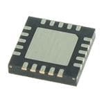
| 描述 | IC ADC 16BIT 4CH 250KSPS 20LFCSP |
| 产品分类 | |
| 品牌 | Analog Devices Inc |
| 数据手册 | |
| 产品图片 |
|
| 产品型号 | AD7682BCPZRL7 |
| PCN组件/产地 | |
| PCN设计/规格 | |
| rohs | 无铅 / 符合限制有害物质指令(RoHS)规范要求 |
| 产品系列 | PulSAR® |
| 产品培训模块 | http://www.digikey.cn/PTM/IndividualPTM.page?site=cn&lang=zhs&ptm=19143 |
| 位数 | 16 |
| 供应商器件封装 | 20-LFCSP-VQ(4x4) |
| 其它名称 | AD7682BCPZRL7CT |
| 包装 | 带卷 (TR) |
| 安装类型 | 表面贴装 |
| 封装/外壳 | 20-VFQFN 裸露焊盘,CSP |
| 工作温度 | -40°C ~ 85°C |
| 数据接口 | DSP,MICROWIRE™,QSPI™,串行,SPI™ |
| 标准包装 | 1 |
| 特性 | - |
| 电压源 | 单电源 |
| 转换器数 | 1 |
| 输入数和类型 | 8 个单端,单极4 个差分,双极4 个伪差分,双极 |
| 采样率(每秒) | 250k |


- 商务部:美国ITC正式对集成电路等产品启动337调查
- 曝三星4nm工艺存在良率问题 高通将骁龙8 Gen1或转产台积电
- 太阳诱电将投资9.5亿元在常州建新厂生产MLCC 预计2023年完工
- 英特尔发布欧洲新工厂建设计划 深化IDM 2.0 战略
- 台积电先进制程称霸业界 有大客户加持明年业绩稳了
- 达到5530亿美元!SIA预计今年全球半导体销售额将创下新高
- 英特尔拟将自动驾驶子公司Mobileye上市 估值或超500亿美元
- 三星加码芯片和SET,合并消费电子和移动部门,撤换高东真等 CEO
- 三星电子宣布重大人事变动 还合并消费电子和移动部门
- 海关总署:前11个月进口集成电路产品价值2.52万亿元 增长14.8%


PDF Datasheet 数据手册内容提取
16-Bit, 8-Channel, 250 kSPS PulSAR ADC Known Good Die AD7689-KGD FEATURES FUNCTIONAL BLOCK DIAGRAM 16-bit resolution with no missing codes 0.5V TO VDD – 0.5V 0.5V TO VDD 2.3V TO 5.5V 0.1µF 10µF 8-channel multiplexer with choice of inputs Unipolar single-ended REFIN REF VDD Differential (GND sense) 1.8V Pseudobipolar BANRDE FGAP AD7689-KGD VIO TVODD Throughput: 250 kSPS TEMP INL: −2.5 LSB minimum, ±0.4 LSB typical, +2.5 LSB maximum SENSOR Dynamic range: 93.8 dB IN0 CNV IN1 SINAD: 91 dB typical at 20 kHz, VREF = 5 V IN2 MUX 16-BIT SAR SPI SERIAL SCK THD: −100 dB at 20 kHz IN3 ADC INTERFACE SDO IN4 Analog input range: 0 V to VREF with VREF up to VDD IN5 ONE-POLE DIN IN6 LPF Multiple reference types SEQUENCER IN7 Internal selectable 2.5 V or 4.096 V COM EExxtteerrnnaall (buupf fteor eVdD (Du)p to 4.096 V) GND 15658-005 Figure 1. Composite View Internal temperature sensor (TEMP) Channel sequencer, selectable 1-pole filter, busy indicator GENERAL DESCRIPTION No pipeline delay, SAR architecture The AD7689-KGD is a 8-channel, 16-bit, charge redistribution Single-supply 2.3 V to 5.5 V operation with 1.8 V to 5.5 V successive approximation register (SAR) analog-to-digital logic interface converter (ADC) that operates from a single power supply, VDD. Serial interface compatible with SPI, MICROWIRE, QSPI, and DSP The AD7689-KGD contains all components for use in a multi- Power dissipation channel, low power data acquisition system, including a true 3.5 mW at 2.5 V, 200 kSPS 16-bit SAR ADC with no missing codes; an 8-channel low 12.5 mW at 5 V, 250 kSPS crosstalk multiplexer that is useful for configuring the inputs Standby current: 50 nA as single-ended (with or without ground sense), differential, or Low cost grade available bipolar; an internal low drift reference (selectable 2.5 V or 4.096 V) Known Good Die (KGD): these die are fully guaranteed to and buffer; a temperature sensor; a selectable one-pole filter; data sheet specifications. and a sequencer that is useful when channels are continuously scanned in order. APPLICATIONS The AD7689-KGD uses a simple SPI interface for writing to the Multichannel system monitoring configuration register and receiving conversion results. The SPI Battery-powered equipment interface uses a separate supply, VIO, which is set to the host Medical instruments: ECG/EKG logic level. Power dissipation scales with throughput. Mobile communications: GPS Power line monitoring The AD7689-KGD is specified from −40°C to +85°C. Data acquisition Additional application and technical information can be found Seismic data acquisition systems in the AD7689 data sheet. Instrumentation Process control Rev. B Document Feedback Information furnished by Analog Devices is believed to be accurate and reliable. However, no responsibility is assumed by Analog Devices for its use, nor for any infringements of patents or other One Technology Way, P.O. Box 9106, Norwood, MA 02062-9106, U.S.A. rights of third parties that may result from its use. Specifications subject to change without notice. No license is granted by implication or otherwise under any patent or patent rights of Analog Devices. Tel: 781.329.4700 ©2017–2018 Analog Devices, Inc. All rights reserved. Trademarks and registered trademarks are the property of their respective owners. Technical Support www.analog.com
AD7689-KGD Known Good Die TABLE OF CONTENTS Features .............................................................................................. 1 Absolute Maximum Ratings ............................................................8 Applications ....................................................................................... 1 ESD Caution...................................................................................8 Functional Block Diagram .............................................................. 1 Pin Configuration and Function Descriptions ..............................9 General Description ......................................................................... 1 Outline Dimensions ....................................................................... 10 Revision History ............................................................................... 2 Die Specifications and Assembly Recommendations ........... 10 Specifications ..................................................................................... 3 Ordering Guide .......................................................................... 10 Timing Specifications .................................................................. 6 REVISION HISTORY 2/2018—Rev. A to Rev. B 7/2017—Revision 0: Initial Version Changes to Features Section............................................................ 1 Changes to Table 1 ............................................................................ 3 10/2017—Rev. 0 to Rev. A Changed Metal Mask Die Image Section to Functional Block Diagram Section ............................................................................... 1 Changes to Figure 1 .......................................................................... 1 Rev. B | Page 2 of 10
Known Good Die AD7689-KGD SPECIFICATIONS VDD = 2.3 V to 5.5 V, VIO = 1.8 V to VDD, REF voltage (V ) = VDD, all specifications T to T , unless otherwise noted. REF MIN MAX Table 1. Parameter Test Conditions/Comments Min Typ Max Unit RESOLUTION 16 Bits ANALOG INPUT Voltage Range Unipolar mode 0 +V V REF Bipolar mode −V /2 +V /2 REF REF Absolute Input Voltage Positive input, unipolar and bipolar modes −0.1 V + 0.1 V REF Negative or COM input, unipolar mode −0.1 +0.1 V Negative or COM input, bipolar mode V /2 − 0.1 V /2 V /2 + 0.1 V REF REF REF Analog Input Common-Mode Rejection Input frequency (f ) = 250 kHz 68 dB IN Ratio (CMRR) Leakage Current at 25°C Acquisition phase 1 nA THROUGHPUT Conversion Rate Full Bandwidth1 VDD = 4.5 V to 5.5 V 0 250 kSPS VDD = 2.3 V to 4.5 V 0 200 kSPS ¼ Bandwidth1 VDD = 4.5 V to 5.5 V 0 62.5 kSPS VDD = 2.3 V to 4.5 V 0 50 kSPS Transient Response Full-scale step, full bandwidth 1.8 µs Full-scale step, ¼ bandwidth 14.5 µs ACCURACY No Missing Codes 16 Bits Integral Linearity Error −2.5 ±0.4 +2.5 LSB2 Differential Linearity Error −1 ±0.25 +2 LSB2 Transition Noise REF = VDD = 5 V 0.5 LSB2 Gain Error −24 ±1 +24 LSB2 Gain Error Match −4 ±0.5 +4 LSB2 Gain Error Temperature Drift ±1 ppm/°C Offset Error VDD = 4.5 V to 5.5 V −8 ±1 +8 LSB2 VDD = 2.3 V to 4.5 V ±5 LSB2 Offset Error Match −4 ±0.5 +4 LSB2 Offset Error Temperature Drift ±1 ppm/°C Power Supply Sensitivity VDD = 5 V ± 5% ±1.5 LSB2 AC ACCURACY3 Dynamic Range 93.8 dB4 Signal-to-Noise Ratio (SNR) f = 20 kHz, V = 5 V 88.5 91 dB4 IN REF f = 20 kHz, V = 4.096 V, internal REF 87 90.5 dB4 IN REF f = 20 kHz, V = 2.5 V, internal REF 83.5 86 dB4 IN REF Signal-to-Noise-And-Distortion Ratio (SINAD) f = 20 kHz, V = 5 V 88.5 91 dB4 IN REF f = 20 kHz, V = 5 V, −60 dB input 33.5 dB4 IN REF f = 20 kHz, V = 4.096 V internal REF 87.5 90 dB4 IN REF f = 20 kHz, V = 2.5 V internal REF 84.5 86 dB4 IN REF Total Harmonic Distortion (THD) f = 20 kHz −100 dB4 IN Spurious-Free Dynamic Range (SFDR) f = 20 kHz 110 dB4 IN Channel to Channel Crosstalk f = 100 kHz on adjacent channel(s) −125 dB4 IN Rev. B | Page 3 of 10
AD7689-KGD Known Good Die Parameter Test Conditions/Comments Min Typ Max Unit SAMPLING DYNAMICS −3 dB Input Bandwidth Full bandwidth 1.7 MHz ¼ bandwidth 0.425 MHz Aperture Delay VDD = 5 V 2.5 ns 1 The bandwidth is set in the configuration register. 2 LSB means least significant bit. With the 5 V input range, one LSB is 76.3 µV. 3 With VDD = 5 V, unless otherwise noted. 4 All specifications expressed in decibels are referred to a full-scale input FSR and tested with an input signal at 0.5 dB below full scale, unless otherwise specified. Rev. B | Page 4 of 10
Known Good Die AD7689-KGD VDD = 2.3 V to 5.5 V, VIO = 1.8 V to VDD, V = VDD, all specifications T to T , unless otherwise noted. REF MIN MAX Table 2. Parameter Test Conditions/Comments Min Typ Max Unit INTERNAL REFERENCE REF Output Voltage 2.5 V at 25°C 2.490 2.500 2.510 V 4.096 V at 25°C 4.086 4.096 4.106 V REFIN Output Voltage1 2.5 V at 25°C 1.2 V 4.096 V at 25°C 2.3 V REF Output Current ±300 µA Temperature Drift ±10 ppm/°C Line Regulation VDD = 5 V ± 5% ±15 ppm/V Long-Term Drift 1000 hours 50 ppm Turn-On Settling Time Reference capacitance (C ) = 10 µF 5 ms REF EXTERNAL REFERENCE Voltage Range REF input 0.5 VDD + 0.3 V REFIN input (buffered) 0.5 VDD − 0.5 V Current Drain2 250 kSPS, REF = 5 V 50 µA TEMPERATURE SENSOR Output Voltage3 25°C 283 mV Temperature Sensitivity 1 mV/°C DIGITAL INPUTS Logic Levels Input Voltage Low, V −0.3 +0.3 × VIO V IL High, V 0.7 × VIO VIO + 0.3 V IH Input Current Low, I −1 +1 µA IL High, I −1 +1 µA IH DIGITAL OUTPUTS Data Format4 Pipeline Delay5 Output Voltage Low, V Sink current (I ) = 500 µA 0.4 V OL SINK High, V Source current (I ) = −500 µA VIO − 0.3 V OH SOURCE POWER SUPPLIES VDD6 Specified performance 2.3 5.5 V VIO Specified performance 1.8 VDD + 0.3 V Standby Current7, 8 VDD and VIO = 5 V at 25°C 50 nA Power Dissipation VDD = 2.5 V, 100 SPS throughput 1.7 µW VDD = 2.5 V, 200 kSPS throughput 3.5 mW VDD = 5 V, 250 kSPS throughput 12.5 18 mW VDD = 5 V, 250 kSPS throughput with internal reference 15.5 21 mW Energy per Conversion VDD = 5 V 60 nJ TEMPERATURE RANGE9 Specified Performance T to T −40 +85 °C MIN MAX 1 This is the output from the internal band gap. 2 This is an average current and scales with throughput. 3 The output voltage is internal and present on a dedicated multiplexer input. 4 Unipolar mode is serial 16-bit straight binary. Bipolar mode is serial 16-bit twos complement. 5 Conversion results available immediately after completed conversion. 6 The minimum VDD supply must be 3 V when the 2.5 V internal reference is enabled, and 4.5 V when the 4.096 V internal reference is enabled. 7 With all digital inputs forced to VIO or GND as required. 8 During acquisition phase. 9 Contact an Analog Devices, Inc., sales representative for the extended temperature range. Rev. B | Page 5 of 10
AD7689-KGD Known Good Die TIMING SPECIFICATIONS VDD = 4.5 V to 5.5 V, VIO = 1.8 V to VDD, all specifications T to T , unless otherwise noted. MIN MAX Table 3. Parameter1 Symbol Min Typ Max Unit CONVERSION TIME CNV Rising Edge to Data Available t 2.2 µs CONV ACQUISITION TIME t 1.8 µs ACQ TIME BETWEEN CONVERSIONS t 4.0 µs CYC DATA WRITE/READ DURING CONVERSION t 1.2 µs DATA SCK Period t t + 2 ns SCK DSDO Low Time t 11 ns SCKL High Time t 11 ns SCKH Falling Edge to Data Remains Valid t 4 ns HSDO Falling Edge to Data Valid Delay t DSDO VIO Above 2.7 V 18 ns VIO Above 2.3 V 23 ns VIO Above 1.8 V 28 ns CNV Pulse Width t 10 ns CNVH Low to SDO D15 MSB Valid t EN VIO Above 2.7 V 18 ns VIO Above 2.3 V 22 ns VIO Above 1.8 V 25 ns High or Last SCK Falling Edge to SDO High Impedance t 32 ns DIS Low to SCK Rising Edge t 10 ns CLSCK DIN Valid Setup Time from SCK Rising Edge t 5 ns SDIN Valid Hold Time from SCK Rising Edge t 5 ns HDIN 1 See Figure 2 and Figure 3 for load conditions. Rev. B | Page 6 of 10
Known Good Die AD7689-KGD VDD = 2.3 V to 4.5 V, VIO = 1.8 V to VDD, all specifications T to T , unless otherwise noted. MIN MAX Table 4. Parameter1 Symbol Min Typ Max Unit CONVERSION TIME t 3.2 µs CONV CNV Rising Edge to Data Available ACQUISITION TIME t 1.8 µs ACQ TIME BETWEEN CONVERSIONS t 5 µs CYC DATA WRITE/READ DURING CONVERSION t 1.2 µs DATA SCK Period t t + 2 ns SCK DSDO Low Time t 12 ns SCKL High Time t 12 ns SCKH Falling Edge to Data Remains Valid t 5 ns HSDO Falling Edge to Data Valid Delay t DSDO VIO Above 3 V 24 ns VIO Above 2.7 V 30 ns VIO Above 2.3 V 38 ns VIO Above 1.8 V 48 ns CNV Pulse Width t 10 ns CNVH Low to SDO D15 MSB Valid t EN VIO Above 3 V 21 ns VIO Above 2.7 V 27 ns VIO Above 2.3 V 35 ns VIO Above 1.8 V 45 ns High or Last SCK Falling Edge to SDO High Impedance t 50 ns DIS Low to SCK Rising Edge t 10 ns CLSCK DIN Valid Setup Time from SCK Rising Edge t 5 ns SDIN Valid Hold Time from SCK Rising Edge t 5 ns HDIN 1 See Figure 2 and Figure 3 for load conditions. 500µA IOL TOSDO 1.4V CL 50pF 500µA IOH 15658-002 Figure 2. Load Circuit for Digital Interface Timing 70% VIO 30% VIO tDELAY tDELAY 2V OR VIO – 0.5V1 2V OR VIO – 0.5V1 0.8V OR 0.5V2 0.8V OR 0.5V2 1220V.8 VIF I FV IVOI OA BAOBVOEV E2. 52V.5,V V, I0O.5 –V 0I.F5 VV IIOF VBIEOL OBEWL 2O.W5V .2.5V. 15658-003 Figure 3. Voltage Levels for Timing Rev. B | Page 7 of 10
AD7689-KGD Known Good Die ABSOLUTE MAXIMUM RATINGS Stresses at or above those listed under Absolute Maximum Table 5. Ratings may cause permanent damage to the product. This is a Parameter Rating stress rating only; functional operation of the product at these Analog Inputs or any other conditions above those indicated in the operational IN0 to IN7, COM GND − 0.3 V to VDD + 0.3 V or VDD ± 130 mA section of this specification is not implied. Operation beyond REF, REFIN GND − 0.3 V to VDD + 0.3 V the maximum operating conditions for extended periods may Supply Voltages affect product reliability. VDD, VIO to GND −0.3 V to +7 V ESD CAUTION VIO to VDD −0.3 V to VDD + 0.3 V DIN, CNV, SCK to GND −0.3 V to VIO + 0.3 V SDO to GND −0.3 V to VIO + 0.3 V Storage Temperature Range −65°C to +150°C Junction Temperature 150°C Rev. B | Page 8 of 10
Known Good Die AD7689-KGD PIN CONFIGURATION AND FUNCTION DESCRIPTIONS N DN DN IFE FE DD DD G G R R V V 5 4 3 2 1 20 IN4 6 19 IN3 IN5 7 18 IN2 IN6 8 17 IN1 IN7 9 16 IN0 COM 10 11 12 13 14 15 VIO VNC NID KCS ODS 15658-004 Figure 4. Pad Configuration Table 6. Pad Function Descriptions Pad No. Mnemonic X-Axis (µm) Y-Axis (µm) Pad Type1 Description 1 VDD +650 +1079 AI Power Supply. Nominally 2.5 V to 5.5 V. 2 REF +475 +1078 AI Reference Input/Output. 3 REFIN −473 +1078 AI Internal Reference Output/Reference Buffer Input. 4 GND −659 +1079 P Power Supply Ground. 5 GND −838 +1079 P Power Supply Ground. 6 IN4 −1085 +892 AI Analog Input Channel 4. 7 IN5 −1085 +653 AI Analog Input Channel 5. 8 IN6 −1085 −528 AI Analog Input Channel 6. 9 IN7 −1085 −769 AI Analog Input Channel 7. 10 COM −1085 −1015 P Common Channel Input. All input channels, IN[7:0], can be referenced to a common-mode point of 0 V or V /2 V. REF 11 CNV −519 −1087 DI Conversion Input. On the rising edge, CNV initiates the conversion. During conversion, if CNV is held low, the busy indictor is enabled. 12 DIN −71 −1087 DI Data Input. Use this input for writing to the 14-bit configuration register. The configuration register can be written to during and after conversion. 13 SCK +231 −1087 DI Serial Data Clock Input. This input is used to clock out the data on SDO and clock in data on. 14 SDO +667 −1087 DO Serial Data Output. 15 VIO +1079 −1056 P Input/Output Interface Digital Power. Nominally at the same supply as the host interface (1.8 V, 2.5 V, 3 V, or 5 V). 16 IN0 +1085 −769 AI Analog Input Channel 0. 17 IN1 +1085 −528 AI Analog Input Channel 1. 18 IN2 +1085 +653 AI Analog Input Channel 2. 19 IN3 +1085 +894 AI Analog Input Channel 3. 20 VDD +997 +1079 P Power Supply. Nominally 2.5 V to 5.5 V. 1 AI is analog input, P is power, DI is digital input, and DO is digital output. Rev. B | Page 9 of 10
AD7689-KGD Known Good Die OUTLINE DIMENSIONS 0.25 2.43 SQ 20 65 3 3 2 1 19 7 18 8 17 9 16 10 11 12 13 14 15 A (CTIROCPU0 IVT. ISE0IDW8E)×0.08 SIDE VIEW 03-23-2017- Figure 5. 20-Pad Bare Die [CHIP] (C-20-2) Dimensions shown in millimeters DIE SPECIFICATIONS AND ASSEMBLY RECOMMENDATIONS Table 7. Die Specifications Parameter Value Unit Scribe Line Width 80 × 80 µm Die Size (Maximum Size) 2430 × 2430 µm Thickness 250 µm Bond Pads (Minimum Size) 80 × 80 µm Bond Pad Composition 0.5 AlCu % Backside Standard assembly die attach Not applicable Passivation Oxynitride Not applicable Chip Size 2350 × 2350 µm Table 8. Assembly Recommendations Assembly Component Recommendation Die Attach Epoxy adhesive Bonding Method Gold ball1 or aluminum wedge Bonding Sequence Bond pin five first 1 Evaluate the gold wire for suitability before use at elevated temperatures for extended durations. ORDERING GUIDE Model Temperature Range Package Description Package Option AD7689-KGD-PT −40°C to +85°C 20-Pad Bare Die [CHIP] C-20-2 ©2017–2018 Analog Devices, Inc. All rights reserved. Trademarks and registered trademarks are the property of their respective owners. D15658-0-2/18(B) Rev. B | Page 10 of 10
Mouser Electronics Authorized Distributor Click to View Pricing, Inventory, Delivery & Lifecycle Information: A nalog Devices Inc.: EVAL-AD7682EDZ AD7689ACPZ AD7682BCPZ AD7689BCPZRL7 AD7689BCPZ AD7689ACPZRL7 EVAL- AD7689EDZ AD7682BCPZRL7 AD7689BCBZ-RL7 AD7682BCBZ-RL7