ICGOO在线商城 > AD7545ALNZ
 Datasheet下载
- 型号: AD7545ALNZ
- 制造商: Analog
- 库位|库存: xxxx|xxxx
- 要求:
| 数量阶梯 | 香港交货 | 国内含税 |
| +xxxx | $xxxx | ¥xxxx |
查看当月历史价格
查看今年历史价格
AD7545ALNZ产品简介:
ICGOO电子元器件商城为您提供AD7545ALNZ由Analog设计生产,在icgoo商城现货销售,并且可以通过原厂、代理商等渠道进行代购。 提供AD7545ALNZ价格参考以及AnalogAD7545ALNZ封装/规格参数等产品信息。 你可以下载AD7545ALNZ参考资料、Datasheet数据手册功能说明书, 资料中有AD7545ALNZ详细功能的应用电路图电压和使用方法及教程。
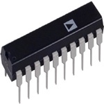
AD7545ALNZ是Analog Devices Inc.(ADI)推出的一款12位并行输入、电流输出型数模转换器(DAC),采用CMOS工艺,具有低功耗、高精度和良好的温度稳定性(±1 LSB积分非线性,工作温度范围–40°C至+85°C),封装为20引脚DIP(LZ后缀表示无铅、符合RoHS)。

其典型应用场景包括:
1. 工业过程控制:用于PLC模拟量输出模块,将控制器数字信号转换为精确电流信号(如4–20 mA环路驱动需外接运算放大器和晶体管),实现对阀门、变频器等执行机构的闭环调节;
2. 自动测试设备(ATE):作为精密波形发生与偏置电压源,配合高速采样电路生成校准用基准信号;
3. 仪器仪表:在数字万用表、示波器校准电路或信号源中提供高稳定度直流偏置或增益调节参考;
4. 军事/航空电子系统:凭借宽温特性和高可靠性,适用于机载传感器信号调理、雷达波束成形控制等对长期稳定性要求严苛的场景。

需注意:AD7545ALNZ为电流输出型,典型应用需外接I/V转换运放(如OP27)以获得电压输出;其单电源(+15 V)或双电源(±15 V)供电支持灵活配置,但设计时需重视参考电压(VREF)精度与噪声抑制,推荐使用ADR291等低温漂基准源。该器件已停产,现多用于维护升级或对成本与供货稳定性要求不高的传统设备中。
| 参数 | 数值 |
| 产品目录 | 集成电路 (IC)半导体 |
| 描述 | IC DAC 12BIT W/BUFF MULT 20-DIP数模转换器- DAC 12B CMOS IC Buffered Multiplying |
| 产品分类 | |
| 品牌 | Analog Devices |
| 产品手册 | |
| 产品图片 |
|
| rohs | 符合RoHS无铅 / 符合限制有害物质指令(RoHS)规范要求 |
| 产品系列 | 数据转换器IC,数模转换器- DAC,Analog Devices AD7545ALNZ- |
| 数据手册 | |
| 产品型号 | AD7545ALNZ |
| 产品培训模块 | http://www.digikey.cn/PTM/IndividualPTM.page?site=cn&lang=zhs&ptm=19145http://www.digikey.cn/PTM/IndividualPTM.page?site=cn&lang=zhs&ptm=18614http://www.digikey.cn/PTM/IndividualPTM.page?site=cn&lang=zhs&ptm=26125http://www.digikey.cn/PTM/IndividualPTM.page?site=cn&lang=zhs&ptm=26140http://www.digikey.cn/PTM/IndividualPTM.page?site=cn&lang=zhs&ptm=26150http://www.digikey.cn/PTM/IndividualPTM.page?site=cn&lang=zhs&ptm=26147 |
| 产品种类 | 数模转换器- DAC |
| 位数 | 12 |
| 供应商器件封装 | 20-PDIP |
| 分辨率 | 12 bit |
| 包装 | 管件 |
| 商标 | Analog Devices |
| 安装类型 | 通孔 |
| 安装风格 | Through Hole |
| 封装 | Tube |
| 封装/外壳 | 20-DIP(0.300",7.62mm) |
| 封装/箱体 | PDIP-20 |
| 工作温度 | 0°C ~ 70°C |
| 工厂包装数量 | 18 |
| 建立时间 | 2µs |
| 接口类型 | Parallel |
| 数据接口 | - |
| 最大功率耗散 | 450 mW |
| 最大工作温度 | + 70 C |
| 最小工作温度 | 0 C |
| 标准包装 | 18 |
| 电压参考 | 10 V |
| 电压源 | 单电源 |
| 电源电压-最大 | 15 V |
| 电源电压-最小 | 5 V |
| 积分非线性 | +/- 0.5 LSB |
| 稳定时间 | 1 us |
| 系列 | AD7545A |
| 结构 | R-2R |
| 转换器数 | 1 |
| 转换器数量 | 1 |
| 输出数和类型 | 1 电流,单极1 电流,双极 |
| 输出类型 | Voltage Buffered |
| 采样率(每秒) | - |


- 商务部:美国ITC正式对集成电路等产品启动337调查
- 曝三星4nm工艺存在良率问题 高通将骁龙8 Gen1或转产台积电
- 太阳诱电将投资9.5亿元在常州建新厂生产MLCC 预计2023年完工
- 英特尔发布欧洲新工厂建设计划 深化IDM 2.0 战略
- 台积电先进制程称霸业界 有大客户加持明年业绩稳了
- 达到5530亿美元!SIA预计今年全球半导体销售额将创下新高
- 英特尔拟将自动驾驶子公司Mobileye上市 估值或超500亿美元
- 三星加码芯片和SET,合并消费电子和移动部门,撤换高东真等 CEO
- 三星电子宣布重大人事变动 还合并消费电子和移动部门
- 海关总署:前11个月进口集成电路产品价值2.52万亿元 增长14.8%


PDF Datasheet 数据手册内容提取
a CMOS 12-Bit Buffered Multiplying DAC AD7545 FEATURES FUNCTIONAL BLOCK DIAGRAM 12-Bit Resolution Low Gain TC: 2 ppm/(cid:1)C typ RFB Fast TTL Compatible Data Latches 20 Single +5 V to +15 V Supply AD7545 R Small 20-Lead 0.3" DIP and 20-Terminal Surface Mount 1 OUT 1 Packages 12-BIT VREF 19 MULTIPLYING DAC Latch Free (Schottky Protection Diode Not Required) 2 AGND Low Cost 12 Ideal for Battery Operated Equipment WR 17 18 VDD INPUT DATA LATCHES CS 16 3 DGND 12 DB11–DB0 (PINS 4–15) GENERAL DESCRIPTION The AD7545 is particularly suitable for single supply operation The AD7545 is a monolithic 12-bit CMOS multiplying DAC and applications with wide temperature variations. with onboard data latches. It is loaded by a single 12-bit wide The AD7545 can be used with any supply voltage from +5 V to word and directly interfaces to most 12- and 16-bit bus systems. +15 V. With CMOS logic levels at the inputs the device dissi- Data is loaded into the input latches under the control of the CS pates less than 0.5 mW for V = +5 V. and WR inputs; tying these control inputs low makes the input DD latches transparent, allowing direct unbuffered operation of the DAC. PIN CONFIGURATIONS DIP LCCC PLCC OAGUTN D1 12 2190 VRRFBEF DGND3 AGND2 OUT 11 2RFB0 1V9REF DGND3 AGND2 OUT 11 2RFB0 1V9REF DGND 3 18 VDD DB11 (MSB) 4 17 WR DB11 (MSB)4 18 VDD DB11 (MSB) 4 PIDINE N1TIFIER 18 VDD DB10 5 AD7545 16 CS DB105 AD7545 17 WR DB10 5 AD7545 17 WR DB9 6 (NToOt Pto V SIEcaWle) 15 DB0 (MSB) DDBB9867 (NToOt Pto V SIEcaWle) 1156 CDSB0 (LSB) DDBB98 67 (NToOt Pto V SIEcaWle) 1165 CDSB0 (LSB) DB8 7 14 DB1 DB78 14 DB1 DB7 8 14 DB1 DB7 8 13 DB2 DB6 9 12 DB3 9 10 11 12 13 9 10 11 12 13 DB5 10 11 DB4 DB6 DB5 DB4 DB3 DB2 DB6 DB5 DB4 DB3 DB2 REV.A Information furnished by Analog Devices is believed to be accurate and reliable. However, no responsibility is assumed by Analog Devices for its use, nor for any infringements of patents or other rights of third parties One Technology Way, P.O. Box 9106, Norwood, MA 02062-9106, U.S.A. which may result from its use. No license is granted by implication or Tel: 617/329-4700 World Wide Web Site: http://www.analog.com otherwise under any patent or patent rights of Analog Devices. Fax: 617/326-8703 © Analog Devices, Inc., 1997
AD7545–SPECIFICATIONS (V = +10 V, V = O V, AGND = DGND unless otherwise noted) REF OUT1 V = +5 V V = +15 V DD DD Limits Limits Parameter Version T = + 25(cid:1)C T T 1 T = + 25(cid:1)C T T 1 Units Test Conditions/Comments A MIN, MAX A MIN, MAX STATIC PERFORMANCE Resolution All 12 12 12 12 Bits J, A, S ±2 ±2 ±2 ±2 LSB max K, B, T ±1 ±1 ±1 ±1 LSB max L, C, U ±1/2 ±1/2 ±1/2 ±1/2 LSB max GL, GC, GU ±1/2 ±1/2 ±1/2 ±1/2 LSB max Differential Nonlinearity J, A, S ±4 ±4 ±4 ±4 LSB max 10-Bit Monotonic T to T MIN MAX K, B, T ±1 ±1 ±1 ±1 LSB max 12-Bit Monotonic T to T MIN MAX L, C, U ±1 ±1 ±1 ±1 LSB max 12-Bit Monotonic T to T MIN MAX GL, GC, GU ±1 ±1 ±1 ±1 LSB max 12-Bit Monotonic T to T MIN MAX Gain Error (Using Internal RFB)2 J, A, S ±20 ±20 ±25 ±25 LSB max DAC Register Loaded with K, B, T ±10 ±10 ±15 ±15 LSB max 111111111111 L, C, U ±5 ±6 ±10 ±10 LSB max Gain Error Is Adjustable Using GL, GC, GU ±1 ±2 ±6 ±7 LSB max the Circuits of Figures 4, 5, and 6 Gain Temperature Coefficient3 ∆Gain/∆Temperature All ±5 ±5 ±10 ±10 ppm/°C max Typical Value is 2 ppm/°C for V = +5 V DD DC Supply Rejection3 ∆Gain/∆V All 0.015 0.03 0.01 0.02 % per % max ∆V = ±5% DD DD Output Leakage Current at OUT1 J, K, L, GL 10 50 10 50 nA max DB0–DB11 = 0 V; WR, CS = 0 V A, B, C, GC 10 50 10 50 nA max S, T, U, GU 10 200 10 200 nA max DYNAMIC PERFORMANCE Current Settling Time3 All 2 2 2 2 µs max To 1/2 LSB. OUT1 Load = 100 Ω. DAC Output Measured from Falling Edge of WR, CS = 0. Propagation Delay3 (from Digital Input Change to 90% of Final Analog Output) All 300 – 250 – ns max OUT1 Load = 100 Ω, C = 13 pF4 EXT Digital-to-Analog Glitch Inpulse All 400 – 250 – nV sec typ V = AGND REF AC Feedthrough5 At OUT1 All 5 5 5 5 mV p-p typ V = ±10 V, 10 kHz Sinewave REF REFERENCE INPUT Input Resistance All 7 7 7 7 kΩ min Input Resistance TC = –300 ppm/°C typ (Pin 19 to GND) 25 25 25 25 kΩ max Typical Input Resistance = 11 kΩ ANALOG OUTPUT Output Capacitance3 C All 70 70 70 70 pF max DB0–DB11 = 0 V, WR, CS = 0 V OUT1 C 200 200 200 200 pF max DB0–DB11 = V , WR, CS = 0 V OUT1 DD DIGITAL INPUTS Input High Voltage V All 2.4 2.4 13.5 13.5 V min IH Input Low Voltage V All 0.8 0.8 1.5 1.5 V max IL Input Current6 I All ±1 ±10 ±1 ±10 µA max V = 0 or V IN IN DD Input Capacitance3 DB0–DB11 All 5 5 5 5 pF max V = 0 IN WR, CS All 20 20 20 20 pF max V = 0 IN SWITCHING CHARACTERISTICS7 Chip Select to Write Setup Time All 280 380 180 200 ns min See Timing Diagram t 200 270 120 150 ns typ CS Chip Select to Write Hold Time t All 0 0 0 0 ns min CH Write Pulse Width t All 250 400 160 240 ns min t ≥ t , t ≥ 0 WR CS WR CH 175 280 100 170 ns typ Data Setup Time All 140 210 90 120 ns min t 100 150 60 80 ns typ DS Data Hold Time t All 10 10 10 10 ns min DH POWER SUPPLY I All 2 2 2 2 mA max All Digital Inputs V or V DD IL IH 100 500 100 500 µA max All Digital Inputs 0 V to V DD 10 10 10 10 µA typ All Digital Inputs 0 V to V DD NOTES 1Temperature range as follows: J, K, L, GL versions, 0°C to +70°C; A, B, C, GC versions, –25°C to +85°C; S, T, U GU versions, –55°C to +125°C. 2This includes the effect of 5 ppm max gain TC. 3Guaranteed but not tested. 4DB0–DB11 = 0 V to VDD or VDD to 0 V. 5Feedthrough can be further reduced by connecting the metal lid on the ceramic package (Suffix D) to DGND. 6Logic inputs are MOS gates. Typical input current (+25°C) is less than 1 nA. 7Sample tested at +25°C to ensure compliance. Specifications subject to change without notice. –2– REV. A
AD7545 CHIP tCS tCH VDD WRITE MODE: MODE SELHEOCLTDIO MNODE: SELECT 0 CS AND WR LOW, DAC RESPONDS EITHER CS OR WR HIGH, DATA BUS TO DATA BUS (DB0–DB11) INPUTS. (DB0–DB11) IS LOCKED OUT; DAC tWR VDD HWORL ODRS CLSA SATS DSUAMTAE DP RHEIGSHE NSTT AWTHEE.N WRITE 0 NOTES: tDS tDH VVDDDD == ++51V5V; t;r t r= = tf t =f = 2 04n0nss DATA IN VIH DATA VALID VDD A90L%L IONFP UVDTD S.IGNAL RISE AND FALL TIMES MEASURED FROM 10% TO (DB0–DB11) VIL 0 TIMING MEASUREMENT REFERENCE LEVEL IS VIH + VIL/2. Write Cycle Timing Diagram ABSOLUTE MAXIMUM RATINGS* Commercial (J, K, L, GL) Grades . . . . . . . . 0°C to +70°C (T = + 25°C unless otherwise noted) Industrial (A, B, C, GC) Grades . . . . . . . . –25°C to +85°C A Extended (S, T, U, GU) Grades . . . . . . . –55°C to +125°C V to DGND . . . . . . . . . . . . . . . . . . . . . . . . . . . –0.3, +17 V DD Storage Temperature . . . . . . . . . . . . . . . . . . –65°C to +150°C Digital Input Voltage to DGND . . . . . . . –0.3 V, V +0.3 V V , V to DGND . . . . . . . . . . . . . . . . . . . . . . . D. D. ±25 V Lead Temperature (Soldering, 10 secs) . . . . . . . . . . . +300°C RFB REF V to DGND . . . . . . . . . . . . . . . . . . . . –0.3 V, V +0.3 V *Stresses above those listed under Absolute Maximum Ratings may cause perma- PIN1 DD AGND to DGND . . . . . . . . . . . . . . . . . –0.3 V, V + 0.3 V nent damage to the device. This is a stress rating only; functional operation of the DD Power Dissipation (Any Package) to +75°C . . . . . . . 450 mW device at these or any other conditions above those indicated in the operational sections of this specification is not implied. Exposure to absolute maximum rating Derates above +75°C . . . . . . . . . . . . . . . . . . . . . . 6 mW/°C conditions for extended periods may affect device reliability. Operating Temperature CAUTION ESD (electrostatic discharge) sensitive device. Electrostatic charges as high as 4000V readily WARNING! accumulate on the human body and test equipment and can discharge without detection. Although the AD7545 features proprietary ESD protection circuitry, permanent damage may occur on devices subjected to high energy electrostatic discharges. Therefore, proper ESD precautions are recommended to avoid performance degradation or loss of functionality. ESD SENSITIVE DEVICE TERMINOLOGY ORDERING GUIDE1 RELATIVE ACCURACY The amount by which the D/A converter transfer function Maximum Gain Error differs from the ideal transfer function after the zero and full- Temperature Relative T = +25(cid:1)C Package scale points have been adjusted. This is an endpoint linearity A Model2 Range Accuracy V = +5 V Options3 DD measurement. AD7545JN 0°C to +70°C ±2 LSB ±20 LSB N-20 AD7545AQ –25°C to +85°C ±2 LSB ±20 LSB Q-20 DIFFERENTIAL NONLINEARITY AD7545SQ –55°C to +125°C ±2 LSB ±20 LSB Q-20 The difference between the measured change and the ideal AD7545KN 0°C to +70°C ±1 LSB ±10 LSB N-20 AD7545BQ –25°C to +85°C ±1 LSB ±10 LSB Q-20 change between any two adjacent codes. If a device has a differ- AD7545TQ –55°C to +125°C ±1 LSB ±10 LSB Q-20 ential nonlinearity of less than 1 LSB it will be monotonic, i.e., AD7545LN 0°C to +70°C ±1/2 LSB ±5 LSB N-20 the output will always increase for an increase in digital code AD7545CQ –25°C to +85°C ±1/2 LSB ±5 LSB Q-20 applied to the D/A converter. AD7545UQ –55°C to +125°C ±1/2 LSB ±5 LSB Q-20 AD7545GLN 0°C to +70°C ±1/2 LSB ±1 LSB N-20 AD7545GCQ –25°C to +85°C ±1/2 LSB ±1 LSB Q-20 PROPAGATION DELAY AD7545GUQ –55°C to +125°C ±1/2 LSB ±1 LSB Q-20 This is a measure of the internal delay of the circuit and is mea- AD7545JP 0°C to +70°C ±2 LSB ±20 LSB P-20A sured from the time a digital input changes to the point at which AD7545SE –55°C to +125°C ±2 LSB ±20 LSB E-20A the analog output at OUT1 reaches 90% of its final value. AD7545KP 0°C to +70°C ±1 LSB ±10 LSB P-20A AD7545TE –55°C to +125°C ±1 LSB ±10 LSB E-20A AD7545LP 0°C to +70°C ±1/2 LSB ±5 LSB P-20A DIGITAL-TO-ANALOG GLITCH IMPULSE AD7545UE –55°C to +125°C ±1/2 LSB ±5 LSB E-20A This is a measure of the amount of charge injected from the AD7545GLP 0°C to +70°C ±1/2 LSB ±1 LSB P-20A digital inputs to the analog outputs when the inputs change AD7545GUE –55°C to +125°C ±1/2 LSB ±1 LSB E-20A state. It is usually specified as the area of the glitch in nV secs NOTES and is measured with V = AGND and an ADLH0032CG as 1Analog Devices reserves the right to ship either ceramic (D-20) in lieu of cerdip REF packages (Q-20). the output op amp, C1 (phase compensation) = 33 pF. 2To order MIL-STD-883, Class B process parts, add /883B to part number. Contact local sales office for military data sheet. For U.S. Standard Military DRAWING (SMD) see DESC drawing 5962-87702. 3E = Leadless Ceramic Chip Carrier; N = Plastic DIP; P = Plastic Leaded Chip Carrier; Q = Cerdip. REV. A –3–
AD7545 CIRCUIT INFORMATION—D/A CONVERTER SECTION power supply. To minimize power supply currents it is recom- Figure 1 shows a simplified circuit of the D/A converter section mended that the digital input voltages be as close as practicably of the AD7545 and Figure 2 gives an approximate equivalent possible to the supply rails (V and DGND). DD circuit. Note that the ladder termination resistor is connected to The AD7545 may be operated with any supply voltage in the AGND. R is typically 11 kΩ. range 5 ≤ V ≤ 15 volts. With V = +15 V the input logic DD DD VREF R R R R levels are CMOS compatible only, i.e., 1.5 V and 13.5 V. 2R 2R 2R 2R 2R 2R BASIC APPLICATIONS Figures 4 and 5 show simple unipolar and bipolar circuits using RFB the AD7545. Resistor R1 is used to trim for full scale. The “G” versions (AD7545GLN, AD7545GCQ, AD7545GUD) OUT 1 have a guaranteed maximum gain error of ±1 LSB at +25°C AGND (V = +5 V), and in many applications it should be possible to DD dispense with gain trim resistors altogether. Capacitor C1 provides DB11 DB10 DB9 DB1 DB0 (MSB) (LSB) phase compensation and helps prevent overshoot and ringing when using high speed op amps. Note that all the circuits of Figures 4, 5 Figure 1.Simplified D/A Circuit of AD7545 and 6 have constant input impedance at the V terminal. REF The binary weighted currents are switched between the OUT1 The circuit of Figure 1 can either be used as a fixed reference bus line and AGND by N-channel switches, thus maintaining a D/A converter so that it provides an analog output voltage in the constant current in each ladder leg independent of the switch range 0 to –V (note the inversion introduced by the op amp), state. IN or V can be an ac signal in which case the circuit behaves as IN The capacitance at the OUT1 bus line, C , is code depen- an attenuator (2-Quadrant Multiplier). V can be any voltage OUT1 IN dent and varies from 70 pF (all switches to AGND) to 200 pF in the range –20 ≤ V + 20 volts (provided the op amp can IN (all switches to OUT1). handle such voltages) since V is permitted to exceed V . REF DD Table II shows the code relationship for the circuit of Figure 4. One of the current switches is shown in Figure 2. The input resistance at VREF (Figure 1) is always equal to RLDR (RLDR is VDD R2* the R/2R ladder characteristic resistance and is equal to value C1 “R”). Since RIN at the VREF pin is constant, the reference termi- 18 20 33pF nal can be driven by a reference voltage or a reference current, VDD RFB ac or dc, of positive or negative polarity. (If a current source is VIN OUT1 1 VOUT 19 VREF AD7545 used, a low temperature coefficient external RFB is recommended R1* AGND 2 AD544L to define scale factor.) DGND (SEE TEXT) 3 TO LADDER ANALOG COMMON FROM DB11–DB0 *REFER TO TABLE I INTERFACE LOGIC Figure 4.Unipolar Binary Operation Table I. Recommended Trim Resistor Values vs. Grades for AGND OUT 1 V = +5 V DD Figure 2.N-Channel Current Steering Switch Trim Resistor J/A/S K/B/T L/C/U GL/GC/GU CIRCUIT INFORMATION—DIGITAL SECTION Figure 3 shows the digital structure for one bit. R1 500 Ω 200 Ω 100Ω 20Ω R2 150 Ω 68 Ω 33Ω 6.8Ω The digital signals CONTROL and CONTROL are generated from CS and WR. Table II. Unipolar Binary Code Table for Circuit of Figure 4 TO AGND SWITCH VIN Binary Number in DAC Register Analog Output TO OUT1 SWITCH 4095 INPUT BUFFERS 1 1 1 1 1 1 1 1 1 1 1 1 –V IN 4096 CONTROL CONTROL 2048 Figure 3.Digital Input Structure 1 0 0 0 0 0 0 0 0 0 0 0 –V = –1/2 V IN 4096 IN The input buffers are simple CMOS inverters designed so that when the AD7545 is operated with VDD = 5 V, the buffers con- 1 vert TTL input levels (2.4 V and 0.8 V) into CMOS logic levels. 0 0 0 0 0 0 0 0 0 0 0 1 –V IN 4096 When V is in the region of 2.0 volts to 3.5 volts, the input IN buffers operate in their linear region and draw current from the 0 0 0 0 0 0 0 0 0 0 0 0 0 Volts –4– REV. A
AD7545 Figure 5 and Table III illustrate the recommended circuit and Table IV. 12-Plus Sign Magnitude Code Table for Circuit of code relationship for bipolar operation. The D/A function itself Figure 6 uses offset binary code and inverter U on the MSB line con- 1 Sign Binary Number in DAC verts twos complement input code to offset binary code. If ap- Bit MSB LSB Analog Output, V propriate; inversion of the MSB may be done in software using OUT an exclusive –OR instruction and the inverter omitted. R3, R4 and R5 must be selected to match within 0.01% and they should 4095 0 1 1 1 1 1 1 1 1 1 1 1 1 + V × be the same type of resistor (preferably wire-wound or metal IN 4096 foil), so their temperature coefficients match. Mismatch of R3 0 0 0 0 0 0 0 0 0 0 0 0 0 0 Volts value to R4 causes both offset and full-scale error. Mismatch of 1 0 0 0 0 0 0 0 0 0 0 0 0 0 Volts R5 and R4 and R3 causes full-scale error. 4095 VDD R2* R4 1 1 1 1 1 1 1 1 1 1 1 1 1 – VIN × 4096 20kΩ C1 18 20 33pF VIN R1* 19 VREVFDDAD7R5F4B5 AOGUNTD1 12 A1 1R0Rk63Ω A220Rk5Ω NAoPteP: LSiIgCn AbitT oIfO “0N”S co HnnIeNctTs RS3 to GND. DB11 DB10–DB0 AD544L 5kΩ VOUT Output Offset: (CMOS D/A converters exhibit a code depen- 4 AD544J 10% dent output resistance which, in turn, causes a code dependent U1 11 (SEE TEXT) ANALOG amplifier noise gain. The effect is a code dependent differential COMMON 12 *FOR VALUES OF R1 AND R2 nonlinearity term at the amplifier output that depends on VOS SEE TABLE I. DATA INPUT where V is the amplifier input offset voltage. To maintain OS monotonic operation it is recommended that V be no greater OS Figure 5.Bipolar Operation (Twos Complement Code) than 25 × 10–6) (V ) over the temperature range of operation. REF Table III. Twos Complement Code Table for Circuit of Suitable op amps are AD517L and AD544L. The AD517L is Figure 5 best suited for fixed reference applications with low bandwidth requirements: it has extremely low offset (50 µV) and in most Data Input Analog Output applications will not require an offset trim. The AD544L has a much wider bandwidth and higher slew rate and is recommended 2047 for multiplying and other applications requiring fast settling. An 0 1 1 1 1 1 1 1 1 1 1 1 +V × IN 2048 offset trim on the AD544L may be necessary in some circuits. General Ground Management: AC or transient voltages 1 0 0 0 0 0 0 0 0 0 0 0 1 +V × between AGND and DGND can cause noise injection into the IN 2048 analog output. The simplest method of ensuring that voltages at 0 0 0 0 0 0 0 0 0 0 0 0 0 Volts AGND and DGND are equal is to tie AGND and DGND together at the AD7545. In more complex systems where the 1 AGND and DGND intertie is on the backplane, it is recom- 1 1 1 1 1 1 1 1 1 1 1 1 –V × IN 2048 mended that two diodes be connected in inverse parallel between the AD7545 AGND and DGND pins (IN914 or 2048 equivalent). 1 0 0 0 0 0 0 0 0 0 0 0 –V × IN 2048 Digital Glitches: When WR and CS are both low the latches are transparent and the D/A converter inputs follow the data Figure 6 shows an alternative method of achieving bipolar out- inputs. In some bus systems, data on the data bus is not always put. The circuit operates with sign plus magnitude code and has valid for the whole period during which WR is low and as a the advantage of giving 12-bit resolution in each quadrant, com- result invalid data can briefly occur at the D/A converter inputs pared with 11-bit resolution per quadrant for the circuit of Fig- during a write cycle. Such invalid data can cause unwanted ure 5. The AD7592 is a fully protected CMOS change-over glitches at the output of the D/A converter. The solution to this switch with data latches. R4 and R5 should match each other to problem, if it occurs, is to retime the write pulse WR so that it 0.01% to maintain the accuracy of the D/A converter. Mismatch only occurs when data is valid. between R4 and R5 introduces a gain error. Another cause of digital glitches is capacitive coupling from the VDD R2* digital lines to the OUT1 and AGND terminals. This should be C1 R4 R5 minimized by screening the analog pins of the AD7545 (Pins 1, 18 20 33pF 20kΩ 20kΩ VIN R1* 19 VRVEDFDAD7RF5B45AOGUNTD1 12 AA1D544L 110R0k3%Ω A2AD544JVOUT 2Ph,oi nw1s9 t2,h 2ae0 na)dn f ar3ol oamgn dpth ibnees dt awirgeeiet aanlt Ppoiinnness e1bn8yd aa o ngfdr to h1ue9n pdoaf t ctrkhaacegk Ae r Daunn7d 5b 4see5tpw. aNereaontteed DB11–DB0 3 1/2 AD7592JN from the digital pins by VDD and DGND to aid screening at ANALOG the board level. On-chip capacitive coupling can also give rise COMMON 12 to crosstalk from the digital-to-analog sections of the AD7545, SIGN BIT particularly in circuits with high currents and fast rise and *FOR VALUES OF R1 AND R2 SEE TABLE I. fall times. This type of crosstalk is minimized by using Figure 6.12-Bit Plus Sign Magnitude D/A Converter REV. A –5–
AD7545 V = +5 volts. However, great care should be taken to ensure DD that the +5 V used to power the AD7545 is free from digitally induced noise. +2 Temperature Coefficients: The gain temperature coefficient of the AD7545 has a maximum value of 5 ppm/°C and a typical +1 value of 2 ppm/°C. This corresponds to worst case gain shifts of 2 LSBs and 0.8 LSBs respectively over a 100°C temperature B S range. When trim resistors Rl and R2 are used to adjust full- – L 0 L scale range, the temperature coefficient of R1 and R2 should DN also be taken into account. The reader is referred to Analog –1 Devices Application Note “Gain Error and Gain Temperature Coefficient of CMOS Multiplying DACs,” Publication Number E630–10–6/81. –2 0 5 10 15 SINGLE SUPPLY OPERATION VDD – Volts The ladder termination resistor of the AD7545 (Figure 1) is connected to AGND. This arrangement is particularly suitable Figure 8. Differential Nonlinearity vs. V for Figure 7 DD for single supply operation because OUT1 and AGND may be Circuit. Reference Voltage = 2.5 Volts. Shaded Area Shows biased at any voltage between DGND and VDD. OUT1 and Range of Values of Differential Nonlinearity that Typically AGND should never go more than 0.3 volts less than DGND or Occur for L, C and U Grades. an internal diode will be turned on and a heavy current may flow which will damage the device. (The AD7545 is, however, protected from the SCR latch-up phenomenon prevalent in 0.5 many CMOS devices.) Figure 7 shows the AD7545 connected in a voltage switching 0.0 mode. OUT1 is connected to the reference voltage and AGND is connected to DGND. The D/A converter output voltage is available at the V pin and has a constant output impedance B–0.5 REF S L equal to R. RFB is not used in this circuit. L – N D–1.0 +15V 18 –1.5 REFERENCE 1 OUT1 VDD VOLTAGE AD7545 VREF 19 VO 2 AGND –2.0 DGND 0 5 10 DB11–DB0 3 VREF – Volts 12 Figure 9. Differential Nonlinearity vs. Reference Voltage 15 VOLT CMOS DIGITAL INPUTS for Figure 7 Circuit. V = 15 Volts. Shaded Area Shows DD Figure 7. Single Supply Operation Using Voltage Range of Values of Differential Nonlinearity that Typically Switching Mode Occur for L, C and U Grades. The loading on the reference voltage source is code dependent The circuits of Figures 4, 5 and 6 can all be converted to single and the response time of the circuit is often determined by the supply operation by biasing AGND to some voltage between behavior of the reference voltage with changing load conditions. VDD and DGND. Figure 10 shows the twos complement bipolar circuit of Figure 5 modified to give a range from +2 V to +8 V To maintain linearity, the voltages at OUT1 and AGND should about a “pseudo-analog ground” of 5 V. This voltage range remain within 2.5 volts of each other, for a V of 15 volts. If DD would allow operation from a single V of +10 V to +15 V. V is reduced from 15 V, or the differential voltage between DD DD The AD584 pin-programmable reference fixes AGND at +5 V. OUT1 and AGND is increased to more than 2.5 V, the differ- V is set at +2 V by means of the series resistors R1 and R2. ential nonlinearity of the DAC will increase and the linearity of IN There is no need to buffer the V input to the AD7545 the DAC will be degraded. Figures 8 and 9 show typical curves REF with an amplifier because the input impedance of the D/A con- illustrating this effect for various values of reference voltage and verter is constant. Note, however, that since the temperature V . If the output voltage is required to be offset from ground DD coefficient of the D/A reference input resistance is typically by some value, then OUT1 and AGND may be biased up. The –300 ppm/°C; applications that experience wide temperature effect on linearity and differential nonlinearity will be the same variations may require a buffer amplifier to generate the +2.0 V as reducing V by the amount of the offset. DD at the AD7545 V pin. Other output voltage ranges can be REF obtained by changing R4 to shift the zero point and (R1 + R2) to change the slope, or gain, of the D/A transfer function. V DD must be kept at least 5 V above OUT1 to ensure that linearity is preserved. –6– REV. A
AD7545 VDD = +10V TO +15V Figure 12 shows an alternative approach for use with 8-bit processors which have a full 16-bit wide address bus such as C1 20Rk5Ω 6800, 8080, Z80 This technique uses the 12 lower address lines 18 20 33pF of the processor address bus to supply data to the DAC, thus +2V19 VREVFDDAD7R5F4B5 OUT1 1 A1 10Rk3Ω each AD7545 connected in this way uses 4k bytes of address 10RK1Ω AGND 2 AD544L A2 VO locations. Data is written to the DAC using a single memory MSB DB10–DB0DGND +5V AD544J write instruction. The address field of the instruction is orga- 4 3 VDD 5Rk6Ω nized so that the lower 12 bits contain the data for the DAC and R2 2 1 R4 the upper 4 bits contain the address of the 4k block at which the 2kΩ ATA AD584J 8 33.3kΩ DAC resides. D 4 A15 CMOS DATA BUS 16-BIT ADDRESS BUS VDD = +10V TO +15V A0 4 Figure 10. Single Supply “Bipolar” Twos Complement DB11 D/A Converter ADDRESS 12 DECODE DB0 CPU AD7545 MICROPROCESSOR INTERFACING OF THE AD7545 Q0 The AD7545 can directly interface to both 8- and 16-bit micro- CS processors via its 12-bit wide data latch using standard CS and WR WR WR control signals. A typical interface circuit for an 8-bit processor is shown in D7 DATA BUS Figure 11. This arrangement uses two memory addresses, one D0 for the lower eight bits of data to the DAC and one for the up- per four bits of data into the DAC via the latch. Figure 12.Connecting the AD7545 to 8-Bit Processors via the Address Bus A15 SUPPLEMENTAL APPLICATION MATERIAL ADDRESS BUS For further information on CMOS multiplying D/A converters A0 the reader is referred to the following texts: Q0* CS Application Guide to CMOS Multiplying D/A converters ADDRESS DECODE Q1* available from Analog Devices, Publication Number G479. CS CPU LATCH DB11 Gain Error and Gain Temperature Coefficient of CMOS 4 4 DB8 AD7545 Multiplying DACS—Application Note, Publication Number WR E630–10–6/81 available from Analog Devices. WR WR DB7 8 DB0 D7 8-BIT DATA BUS 8 D0 * Q0 = DECODED ADDRESS FOR DAC Q1 = DECODED ADDRESS FOR LATCH Figure 11.8-Bit Processor to AD7545 Interface REV. A –7–
AD7545 OUTLINE DIMENSIONS Dimensions shown in inches and (mm). 20-Lead Plastic DIP 20-Lead Cerdip 7 (N-20) (Q-20) 9 6/ – 0 – d 0 7 6 C 20-Terminal Leadless Ceramic Chip Carrier (LCCC) 20-Lead Plastic Leaded Chip Carrier (PLCC) (E-20A) (P-20A) A. S. U. N D I E T N RI P –8– REV. A