ICGOO在线商城 > 集成电路(IC) > 数据采集 - 数字电位器 > AD5259BRMZ50

 Datasheet下载
- 型号: AD5259BRMZ50
- 制造商: Analog
- 库位|库存: xxxx|xxxx
- 要求:
| 数量阶梯 | 香港交货 | 国内含税 |
| +xxxx | $xxxx | ¥xxxx |
查看当月历史价格
查看今年历史价格
AD5259BRMZ50产品简介:
ICGOO电子元器件商城为您提供AD5259BRMZ50由Analog设计生产,在icgoo商城现货销售,并且可以通过原厂、代理商等渠道进行代购。 AD5259BRMZ50价格参考¥9.44-¥20.89。AnalogAD5259BRMZ50封装/规格:数据采集 - 数字电位器, Digital Potentiometer 50k Ohm 1 Circuit 256 Taps I²C Interface 10-MSOP。您可以下载AD5259BRMZ50参考资料、Datasheet数据手册功能说明书,资料中有AD5259BRMZ50 详细功能的应用电路图电压和使用方法及教程。
AD5259BRMZ50 是 Analog Devices Inc. 生产的一款数字电位器,属于数据采集类电子元件。该器件具有非易失性存储器,可在断电后保留设定值,适用于需要精密调节电阻的应用场合。

其主要应用场景包括:

1. 工业控制:用于自动控制系统中对电压或电流信号的精确调节,如传感器校准、反馈环路调整等。

2. 通信设备:在光模块或射频电路中进行增益控制、偏置调节,以优化信号传输质量。

3. 测试与测量仪器:用于校正仪表内部基准电压或电流,提高测量精度和稳定性。

4. 医疗设备:在诊断或监测设备中实现参数调节,如放大器增益控制、传感器信号调理等。

5. 消费电子产品:用于音频设备中的音量控制、显示亮度调节等功能,提供更灵活的用户界面体验。

6. 汽车电子:如车载音响系统、环境控制系统中进行参数微调,适应不同工作环境。

AD5259BRMZ50 采用节省空间的 TSSOP 封装,支持 I²C 数字接口控制,便于集成于嵌入式系统中,适合高精度、小体积设计需求。
| 参数 | 数值 |
| 产品目录 | 集成电路 (IC)半导体 |
| 描述 | IC POT DGTL 50K 256POS 10-MSOP数字电位计 IC IC 8-Bit I2C EEMEM |
| DevelopmentKit | EVAL-AD5259DBZ |
| 产品分类 | |
| 品牌 | Analog Devices Inc |
| 产品手册 | |
| 产品图片 |
|
| rohs | 符合RoHS无铅 / 符合限制有害物质指令(RoHS)规范要求 |
| 产品系列 | 数字电位计 IC,Analog Devices AD5259BRMZ50- |
| 数据手册 | |
| 产品型号 | AD5259BRMZ50 |
| POT数量 | Single |
| 产品目录页面 | |
| 产品种类 | 数字电位计 IC |
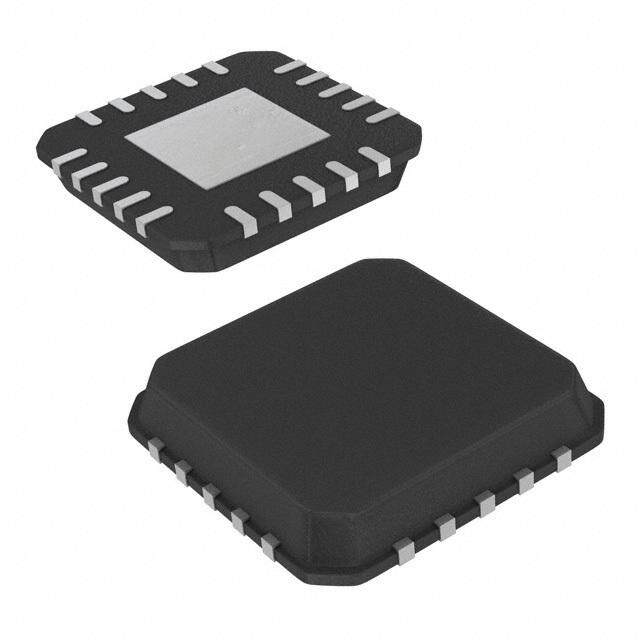
| 供应商器件封装 | 10-MSOP |
| 包装 | 管件 |
| 商标 | Analog Devices |
| 存储器类型 | 非易失 |
| 安装类型 | 表面贴装 |
| 安装风格 | SMD/SMT |
| 容差 | 30 % |
| 封装 | Tube |
| 封装/外壳 | 10-TFSOP,10-MSOP(0.118",3.00mm 宽) |
| 封装/箱体 | MSOP-10 |
| 工作温度 | -40°C ~ 85°C |
| 工作电源电压 | 2.75 V |
| 工厂包装数量 | 50 |
| 弧刷存储器 | Non Volatile |
| 抽头 | 256 |
| 接口 | I²C(设备位址) |
| 描述/功能 | Nonvolatile, I2C Compatible 256-Position, Digital Potentiometer |
| 数字接口 | I2C |
| 最大工作温度 | + 85 C |
| 最小工作温度 | - 40 C |
| 标准包装 | 50 |
| 每POT分接头 | 256 |
| 温度系数 | 标准值 500 ppm/°C |
| 电压-电源 | 2.7 V ~ 3.3 V,4.5 V ~ 5.5 V |
| 电源电压-最大 | 5.5 V |
| 电源电压-最小 | 2.7 V |
| 电源电流 | 3 uA |
| 电路数 | 1 |
| 电阻 | 50 kOhms |
| 电阻(Ω) | 50k |
| 系列 | AD5259 |
| 配用 | /product-detail/zh/AD5259EVAL/AD5259EVAL-ND/993186 |


- 商务部:美国ITC正式对集成电路等产品启动337调查
- 曝三星4nm工艺存在良率问题 高通将骁龙8 Gen1或转产台积电
- 太阳诱电将投资9.5亿元在常州建新厂生产MLCC 预计2023年完工
- 英特尔发布欧洲新工厂建设计划 深化IDM 2.0 战略
- 台积电先进制程称霸业界 有大客户加持明年业绩稳了
- 达到5530亿美元!SIA预计今年全球半导体销售额将创下新高
- 英特尔拟将自动驾驶子公司Mobileye上市 估值或超500亿美元
- 三星加码芯片和SET,合并消费电子和移动部门,撤换高东真等 CEO
- 三星电子宣布重大人事变动 还合并消费电子和移动部门
- 海关总署:前11个月进口集成电路产品价值2.52万亿元 增长14.8%


PDF Datasheet 数据手册内容提取
Nonvolatile, I2C-Compatible 256-Position, Digital Potentiometer Data Sheet AD5259 FEATURES FUNCTIONAL BLOCK DIAGRAMS Nonvolatile memory maintains wiper settings 256-position VDD RDAC A Thin LFCSP-10 (3 mm x 3 mm x 0.8 mm) package VLOGIC EERPDRAOCM RERGDISATCER W GND Compact MSOP-10 (3 mm × 4.9 mm × 1.1mm) package B I2C®-compatible interface 8 DATA SCL VLOGIC pin provides increased interface flexibility SDA SEIR2CIAL 8 CONTROL End-to-end resistance 5 kΩ, 10 kΩ, 50 kΩ, 100 kΩ INTERFACE AD0 COMMAND Resistance tolerance stored in EEPROM (0.1% accuracy) AD1 DECODE LOGIC Power-on EEPROM refresh time < 1ms ADDRESS AD5259 DECODE LOGIC Software write protect command POWER- ON RESET Ad4d preascsk Dageecos dpee rP binu As D0 and Pin AD1 allow CONTROL LOGIC 05026-001 100-year typical data retention at 55°C Figure 1. Block Diagram Wide operating temperature −40°C to +125°C VLOGIC VDD 3 V to 5 V single supply A EEPROM APPLICATIONS SCL RDAC SDA I2C REGISTER LCD panel VCOM adjustment AADD01 INTSEERRFIAALCE SLHAEIFNVTEDELR LCD panel brightness and contrast control W COMMAND Mechanical potentiometer replacement in new designs DECODE LOGIC ADDRESS Programmable power supplies DECODE LOGIC RF amplifier biasing CONTROL LOGIC Automotive electronics adjustment GND B 05026-003 Gain control and offset adjustment Figure 2. Block Diagram Showing Level Shifters Fiber to the home systems Electronics level settings CONNECTION DIAGRAM GENERAL DESCRIPTION W 1 10 A The AD5259 provides a compact, nonvolatile LFCSP-10 AD0 2 AD5259 9 B (3 mm × 3 mm) or MSOP-10 (3 mm × 4.9 mm) packaged AD1 3 TOP VIEW 8 VDD dasose lvmuitceieocshn pa fneorirfc o2arl5 mp6-o pttheoens itstiaioommne ea tedelejruscs1t tromorn evincat ra iadapbjuplesli tcrmeasteiinosttno fsru.s nT, bchtueitos en SSDCAL 45 (Not to Scale) 76 GVLNODGIC 05026-002 Figure 3. Pinout with enhanced resolution and solid-state reliability. The wiper settings are controllable through an I2C-compatible digital interface that is also used to read back the wiper register and EEPROM content. Resistor tolerance is also stored within EEPROM, providing an end-to-end tolerance accuracy of 0.1%. A separate V pin delivers increased interface flexibility. For 1 The terms digital potentiometer, VR (variable resistor), and RDAC are used LOGIC interchangeably. users who need multiple parts on one bus, Address Bit AD0 and Address Bit AD1 allow up to four devices on the same bus. Rev. C Document Feedback Information furnished by Analog Devices is believed to be accurate and reliable. However, no responsibility is assumed by Analog Devices for its use, nor for any infringements of patents or other One Technology Way, P.O. Box 9106, Norwood, MA 02062-9106, U.S.A. rights of third parties that may result from its use. Specifications subject to change without notice. No license is granted by implication or otherwise under any patent or patent rights of Analog Devices. Tel: 781.329.4700 ©2005–2012 Analog Devices, Inc. All rights reserved. Trademarks and registered trademarks are the property of their respective owners. Technical Support www.analog.com
AD5259 Data Sheet TABLE OF CONTENTS Specifications ..................................................................................... 3 I2C-Compatible Format ................................................................. 16 Electrical Characteristics ............................................................. 3 Generic Interface ........................................................................ 16 Timing Characteristics ................................................................ 5 Write Modes ................................................................................ 16 Absolute Maximum Ratings ............................................................ 6 Read Modes ................................................................................. 17 ESD Caution .................................................................................. 6 Store/Restore Modes .................................................................. 17 Pin Configuration and Function Descriptions ............................. 7 Tolerance Readback Modes ...................................................... 18 Typical Performance Characteristics ............................................. 8 ESD Protection of Digital Pins and Resistor Terminals ........ 19 Test Circuits ..................................................................................... 13 Power-Up Sequence ................................................................... 19 Theory of Operation ...................................................................... 14 Layout and Power Supply Bypassing ....................................... 19 Programming the Variable Resistor ......................................... 14 Multiple Devices on One Bus ................................................... 19 Programming the Potentiometer Divider ............................... 14 Evaluation Board ........................................................................ 19 I2C-Compatible Interface............................................................... 15 Display Applications ...................................................................... 20 Writing ......................................................................................... 15 Circuitry ...................................................................................... 20 Storing/Restoring ....................................................................... 15 Outline Dimensions ....................................................................... 21 Reading ........................................................................................ 15 Ordering Guide .......................................................................... 22 REVISION HISTORY 10/12—Rev. B to Rev. C Changed Maximum Temperature Value from 85°C to 125°C 7/05—Rev. 0 to Rev. A (Throughout) .................................................................................... 1 Added 10-Lead LFCSP ...................................................... Universal Changes to Table 1 ............................................................................ 3 Changes to Features Section and Updated Outline Dimensions ....................................................... 21 General Description Section ............................................................ 1 Changes to Ordering Guide .......................................................... 22 Changes to Table 1 ............................................................................. 3 5/10—Rev. A to Rev. B Changes to Table 2 and Added Figure 4 ......................................... 5 Changes to Table 4 ............................................................................. 7 Changes to Figure 5 .......................................................................... 7 Changes to Figure 27 Caption ...................................................... 11 Changes to Storing/Restoring Section ......................................... 15 Changes to Theory of Operation Section.................................... 14 Changes to Table 7 .......................................................................... 16 Changes to I2C-Compatible Interface Section ............................ 15 Changes to Table 14 ........................................................................ 17 Changes to Table 5 .......................................................................... 16 Updated Outline Dimensions ....................................................... 21 Changes to Multiple Devices on One Bus Section ..................... 19 Updated Figure 49 Caption ........................................................... 21 Changes to Ordering Guide .......................................................... 21 2/05—Revision 0: Initial Version Rev. C | Page 2 of 24
Data Sheet AD5259 SPECIFICATIONS ELECTRICAL CHARACTERISTICS V = V = 5 V ± 10% or 3 V ± 10%; V = V ; V = 0 V; −40°C < T < +125°C, unless otherwise noted. DD LOGIC A DD B A Table 1. Parameter Symbol Conditions Min Typ1 Max Unit DC CHARACTERISTICS: RHEOSTAT MODE Resistor Differential Nonlinearity R-DNL RWB, VA = no connect LSB 5 kΩ –1 ±0.2 +1 10 kΩ −1 ±0.1 +1 50 kΩ/100 kΩ −0.5 ±0.1 +0.5 Resistor Integral Nonlinearity R-INL RWB, VA = no connect LSB 5 kΩ –4 ±0.3 +4 10 kΩ −2 ±0.2 +2 50 kΩ/100 kΩ −1 ±0.4 +1 Nominal Resistor Tolerance ΔR T = 25°C, V = 5.5 V –30 +30 % AB A DD Resistance Temperature Coefficient (ΔR x 106)/ Code = 0x00/0x80 500/15 ppm/°C AB (R x ΔT) AB Total Wiper Resistance R Code = 0x00 75 350 Ω WB DC CHARACTERISTICS: POTENTIOMETER DIVIDER MODE Differential Nonlinearity DNL LSB 5 kΩ –1 ±0.2 +1 10 kΩ −0.5 ±0.1 +0.5 50 kΩ/100 kΩ −0.5 ±0.2 +0.5 Integral Nonlinearity INL LSB 5 kΩ –1 ±0.2 +1 10 kΩ −0.5 ±0.1 +0.5 50 kΩ/100 kΩ −0.5 ±0.1 +0.5 Full-Scale Error V Code = 0xFF LSB WFSE 5 kΩ −7 −3 0 10 kΩ −4 −1.5 0 50 kΩ/100 kΩ −1 −0.4 0 Zero-Scale Error V Code = 0x00 WZSE 5 kΩ −40°C < T < +85°C 0 2.5 4 LSB A +85°C < T < +125°C 6 LSB A 10 kΩ −40°C < T < +85°C 0 1 3 LSB A +85°C < T < +125°C 4 LSB A 50 kΩ/100 kΩ 0 0.2 0.5 LSB Voltage Divider Temperature (∆V x 106)/ Code = 0x00/0x80 60/5 ppm/°C W Coefficient (V x ∆T) W RESISTOR TERMINALS Voltage Range V GND V V A, B, W DD Capacitance A, B C f = 1 MHz, measured to GND, 45 pF A, B code = 0x80 Capacitance W C f = 1 MHz, measured to GND, 60 pF W code = 0x80 Common-Mode Leakage I V = V = V /2 10 nA CM A B DD Rev. C | Page 3 of 24
AD5259 Data Sheet Parameter Symbol Conditions Min Typ1 Max Unit DIGITAL INPUTS AND OUTPUTS Input Logic High V 0.7 × V V + 0.5 V IH L L Input Logic Low V −0.5 0.3 × V V IL L Leakage Current I µA IL SDA, AD0, AD1 V = 0 V or 5 V 0.01 ±1 IN SCL – Logic High V = 0 V −2.5 −1.3 +1 IN SCL – Logic Low V = 5 V 0.01 ±1 IN Input Capacitance C 5 pF IL POWER SUPPLIES Power Supply Range V 2.7 5.5 V DD Positive Supply Current I 0.1 2 µA DD Logic Supply V 2.7 5.5 V LOGIC Logic Supply Current I V = 5 V or V = 0 V LOGIC IH IL −40°C < T < +85°C 3 6 µA A +85°C < T < +125°C 9 µA A Programming Mode Current (EEPROM) I V = 5 V or V = 0 V 35 mA LOGIC(PROG) IH IL Power Dissipation P V = 5 V or V = 0 V, V = 5 V 15 40 µW DISS IH IL DD Power Supply Rejection Ratio PSRR V = +5 V ± 10%, code = 0x80 ±0.005 ±0.06 %/% DD DYNAMIC CHARACTERISTICS Bandwidth −3 dB BW Code = 0x80 R = 5 kΩ 2000 kHz AB R = 10 kΩ 800 kHz AB R = 50 kΩ 160 kHz AB R = 100 kΩ 80 kHz AB Total Harmonic Distortion THD R = 10 kΩ, V = 1 V rms, 0.01 % W AB A V = 0, f = 1 kHz B V Settling Time t R = 10 kΩ, V = 5 V, 500 ns W S AB AB ±1 LSB error band Resistor Noise Voltage Density e R = 5 kΩ, f = 1 kHz 9 nV/√Hz N_WB WB 1 Typical values represent average readings at 25°C and V = 5 V. DD Rev. C | Page 4 of 24
Data Sheet AD5259 TIMING CHARACTERISTICS V = V = 5 V ± 10% or 3 V ± 10%; V = V ; V = 0 V; −40°C < T < +125°C, unless otherwise noted. DD LOGIC A DD B A Table 2. Parameter Symbol Conditions Min Typ Max Unit I2C INTERFACE TIMING CHARACTERISTICS1 SCL Clock Frequency f 0 400 kHz SCL t Bus Free Time Between Stop t 1.3 μs BUF 1 and Start t Hold Time (Repeated Start) t After this period, the first clock pulse is 0.6 μs HD;STA 2 generated. t Low Period of SCL Clock t 1.3 μs LOW 3 t High Period of SCL Clock t 0.6 μs HIGH 4 t Setup Time for Repeated t 0.6 μs SU;STA 5 Start Condition t Data Hold Time t 0 0.9 μs HD;DAT 6 t Data Setup Time t 100 ns SU;DAT 7 t Fall Time of Both SDA and t 300 ns F 8 SCL Signals t Rise Time of Both SDA and t 300 ns R 9 SCL Signals t Setup Time for Stop Condition t 0.6 μs SU;STO 10 EEPROM Data Storing Time t 26 ms EEMEM_STORE EEPROM Data Restoring Time at t V rise time dependent. Measure without 300 μs EEMEM_RESTORE1 DD Power On2 decoupling capacitors at V and GND. DD EEPROM Data Restoring Time upon t V = 5 V. 300 μs EEMEM_RESTORE2 DD Restore Command2 EEPROM Data Rewritable Time3 t 540 μs EEMEM_REWRITE FLASH/EE MEMORY RELIABILITY Endurance4 100 700 kCycles Data Retention5 100 Years 1 Standard I2C mode operation guaranteed by design. 2 During power-up, the output is momentarily preset to midscale before restoring EEPROM content. 3 Delay time after power-on PRESET prior to writing new EEPROM data. 4 Endurance is qualified to 100,000 cycles per JEDEC Std. 22 method A117, and is measured at –40°C, +25°C, and +125°C; typical endurance at +25°C is 700,000 cycles. 5 Retention lifetime equivalent at junction temperature (TJ) = 55°C per JEDEC Std. 22, Method A117. Retention lifetime based on an activation energy of 0.6 eV derates with junction temperature. t8 t6 t9 t2 SCL t2 t3 t4 t7 t5 t10 t8 t9 SDA P t1 S S P 05026-004 Figure 4. I2C Interface Timing Diagram Rev. C | Page 5 of 24
AD5259 Data Sheet ABSOLUTE MAXIMUM RATINGS T = 25°C, unless otherwise noted. A Table 3. Stresses above those listed under Absolute Maximum Ratings Parameter Value may cause permanent damage to the device. This is a stress V , V to GND −0.3 V to +7 V DD LOGIC rating only; functional operation of the device at these or any V , V , V to GND GND − 0.3 V, V + 0.3 V A B W DD other conditions above those indicated in the operational I MAX section of this specification is not implied. Exposure to absolute Pulsed1 ±20 mA maximum rating conditions for extended periods may affect Continuous ±5 mA device reliability. Digital Inputs and Output Voltage 0 V to 7 V to GND ESD CAUTION Operating Temperature Range −40°C to +125°C Maximum Junction Temperature 150°C (T ) JMAX Storage Temperature −65°C to +150°C Lead Temperature 300°C (Soldering, 10 sec) Thermal Resistance2 θ : MSOP–10 200°C/W JA 1 Maximum terminal current is bounded by the maximum current handling of the switches, maximum power dissipation of the package, and maximum applied voltage across any two of the A, B, and W terminals at a given resistance. 2 Package power dissipation = (T – T)/θ . JMAX A JA Rev. C | Page 6 of 24
Data Sheet AD5259 PIN CONFIGURATION AND FUNCTION DESCRIPTIONS W 1 10 A AD0 2 AD5259 9 B AD1 3 TOP VIEW 8 VDD SDA 4 (Not to Scale) 7 GND SCL 5 6 VLOGIC NOTES 1 . TBLHEEEF CT EO FXNLPNOOEASCTETIDNE GDP .ATDO SGHNODU OLRD 05026-002 Figure 5. Pin Configuration Table 4. Pin Function Descriptions Pin Mnemonic Description 1 W W Terminal, GND ≤ V ≤ V . W DD 2 ADO Programmable Pin 0 for Multiple Package Decoding. State is registered on power-up. 3 AD1 Programmable Pin 1 for Multiple Package Decoding. State is registered on power-up. 4 SDA Serial Data Input/Output. 5 SCL Serial Clock Input. Positive edge triggered. 6 V Logic Power Supply. LOGIC 7 GND Digital Ground. 8 V Positive Power Supply. DD 9 B B Terminal, GND ≤ V ≤ V . B DD 10 A A Terminal, GND ≤ V ≤ V . A DD 11 EPAD Exposed Pad. The exposed pad should be connected to GND or left floating. Rev. C | Page 7 of 24
AD5259 Data Sheet TYPICAL PERFORMANCE CHARACTERISTICS V = V = 5.5 V, R = 10 kΩ, T = +25°C; unless otherwise noted. DD LOGIC AB A 1.5 0.25 1.3 0.20 2.7V B) 1.1 S 0.15 LSB) 0.9 NL (L 0.10 E INL ( 0.7 ODE D 0.05 D M T MO 0.5 TER 0 A 0.3 E–0.05 T M RHEOS –00..11 OTENTIO––00..1105 +85+°2C5–°4C0°C P ––00..35 5.5V 05026-015 ––00..2205 05026-012 0 32 64 96 128 160 192 224 256 0 32 64 96 128 160 192 224 256 CODE (Decimal) CODE (Decimal) Figure 6. R-INL vs. Code vs. Supply Voltage Figure 9. DNL vs. Code vs. Temperature 0.5 0.25 0.4 0.20 B) 0.3 2.7V LSB) 0.15 NL (LS 0.2 E INL ( 0.10 2.7V 5.5V D 0.1 D 0.05 DE MO O 0 R 0 M E STAT –0.1 OMET–0.05 O –0.2 TI–0.10 HE 5.5V EN R –0.3 OT–0.15 P ––00..45 05026-017 ––00..2205 05026-011 0 32 64 96 128 160 192 224 256 0 32 64 96 128 160 192 224 256 CODE (Decimal) CODE (Decimal) Figure 7. R-DNL vs. Code vs. Supply Voltage Figure 10. INL vs. Supply Voltages 0.25 0.25 0.20 0.20 SB) 0.15 SB) 0.15 POTENTIOMETER MODE INL (L–––––0000000.......100112205050505 TA = +8T5A°C = +25°C TA =–40°C 05026-010 POTENTIOMETER MODE DNL (L–––––0000000.......011221005505050 2.7V 5.5V 05026-013 0 32 64 96 128 160 192 224 256 0 32 64 96 128 160 192 224 256 CODE (Decimal) CODE (Decimal) Figure 8. INL vs. Code vs. Temperature Figure 11. DNL vs. Code vs. Supply Voltage Rev. C | Page 8 of 24
Data Sheet AD5259 0.5 2.0 0.4 1.8 0.3 1.6 LSB) 0.2 1.4 ZSE @ VDD = 2.7V L ( DE IN 0.1 –40°C +25°C SB) 1.2 T MO 0 SE (L 1.0 ZSE @ VDD = 5.5V A –0.1 Z 0.8 T S EO –0.2 0.6 H R –0.3 0.4 ––00..45 +85°C 05026-014 0.20 05026-023 0 32 64 96 128 160 192 224 256 –40 –20 0 20 40 60 80 CODE (Decimal) TEMPERATURE (°C) Figure 12. R-INL vs. Code vs. Temperature Figure 15. Zero-Scale Error vs. Temperature 0.5 1 0.4 0.3 SB) TA =–40°C µA) L (L 0.2 TA = +85°C NT ( DN 0.1 RE DE UR O 0 C M Y EOSTAT ––00..12 TA = +25°C , SUPPLD VDD = 5.5V H D R –0.3 I ––00..45 05026-016 0.1 05026-020 0 32 64 96 128 160 192 224 256 –40 –20 0 20 40 60 80 CODE (Decimal) TEMPERATURE (°C) Figure 13. R-DNL vs. Code vs. Temperature Figure 16. Supply Current vs. Temperature 0 6 –0.5 µA) 5 T ( N E 4 –1.0 RR VDD = 5.5V U FSE (LSB) –1.5 FSE @ VDD = 5.5V C SUPPLY C 32 –2.0 GI LO 1 ––32..05 FSE @ VDD = 2.7V 05026-024 I, LOGIC –10 VDD = 2.7V 05026-021 –40 –20 0 20 40 60 80 –40 –20 0 20 40 60 80 TEMPERATURE (°C) TEMPERATURE (°C) Figure 14. Full-Scale Error vs. Temperature Figure 17. Logic Supply Current vs. Temperature vs. V DD Rev. C | Page 9 of 24
AD5259 Data Sheet 400 100kΩ 120 300 °T MODE TEMPCO (ppm/C) ––2112000000000 50kΩ10kΩ ΩAL RESISTANCE (k) 1086000 15000kkΩΩ R Rt t@ @ V VDDDD = = 5 .55.V5V TA –300 OT 40 OS 5kΩ T 10kΩ Rt @ VDD = 5.5V RHE –––654000000 05026-019 200 5kΩ Rt @ VDD = 5.5V 05026-025 0 32 64 96 128 160 192 224 256 –40 –20 0 20 40 60 80 CODE (Decimal) TEMPERATURE (°C) Figure 18. Rheostat Mode Tempco (ΔRAB x 106)/(RAB x ΔT) vs. Code Figure 21. Total Resistance vs. Temperature 70 0 80H C) 60 –6 °pm/ 50 –12 40H p CO ( 40 –18 20H MP 30 10H R MODE TE 1200 10kΩ 100kΩ GAIN (dB) –––332604 000842HHH OMETE –100 –42 01H TI –48 N –20 POTE ––4300 50kΩ 5kΩ 05026-018 ––6504 05026-026 0 32 64 96 128 160 192 224 256 1k 10k 100k 1M 10M CODE (Decimal) FREQUENCY (Hz) Figure 19. Potentiometer Mode Tempco (ΔVW x 106)/(VW x ΔT) vs. Code Figure 22. Gain vs. Frequency vs. Code, RAB = 5 kΩ 350 0 80H –6 300 40H –12 20H 250 –18 R @ 0x00WB 125000 RWB @ VDD = 2.7V GAIN (dB) –––332604 10000842HHHH –42 100 RWB @ VDD = 5.5V –48 01H 500 05026-022 ––6504 05026-027 –40 –20 0 20 40 60 80 1k 10k 100k 1M 10M TEMPERATURE (°C) FREQUENCY (Hz) Figure 20. RWB vs. Temperature Figure 23. Gain vs. Frequency vs. Code, RAB = 10 kΩ Rev. C | Page 10 of 24
Data Sheet AD5259 0 10k 80H –6 40H –12 –18 20H VDD = VLOGIC = 5V 1k 10H N (dB) ––3204 08H (A)C GAI 04H OGI –36 02H IL 100 VDD = VLOGIC = 3V –42 01H –48 ––6504 05026-028 10 05026-055 1k 10k 100k 1M 0 1 2 3 4 5 FREQUENCY (Hz) VIH (V) Figure 24. Gain vs. Frequency vs. Code, RAB = 50 kΩ Figure 27. Logic Supply Current vs. Input Voltage 0 80 –6 80H CODE = MIDSCALE, VA = VLOGIC, VB = 0V 40H –12 PSRR @ VLOGIC = 5V DC 10% p-p AC 20H 60 –18 GAIN (dB) –––332604 100084HHH PSRR (dB) 40 PSRR @ VLOGIC = 3V DC 10% p-p AC 02H –42 01H 20 –48 ––6504 05026-029 0 05026-054 1k 10k 100k 1M 100 1k 10k 100k 1M FREQUENCY (Hz) FREQUENCY (Hz) Figure 25. Gain vs. Frequency vs. Code, RAB = 100 kΩ Figure 28. PSRR vs. Frequency 0 –6 ––1182 18000kkHz V/DIV 50k m AIN (dB) ––3204 160kHz1800k0kHz5k 200 1 VW G 2MHz –36 –42 V SCL –48 DI V/ 2 ––65041k 10k 100k 1M 10M05026-050 5 05026-051 FREQUENCY (Hz) 400ns/DIV Figure 26. −3 dB Bandwidth @ Code = 0×80 Figure 29. Digital Feedthrough Rev. C | Page 11 of 24
AD5259 Data Sheet V DI V/ 2 V DI VW VW V/ 1 1 m 0 5 V DI V/ 5 SCL 05026-052 2 05026-053 1µs/DIV 200ns/DIV Figure 30. Midscale Glitch, Code 0×7F to 0×80 Figure 31. Large Signal Settling Time Rev. C | Page 12 of 24
Data Sheet AD5259 TEST CIRCUITS Figure 32 through Figure 37 illustrate the test circuits that define the test conditions used in the product Specifications tables. VA V+ = VDD± 10% V+ ADWUT V1L+S =B V =D DV+/2N V+ ∆VDD ADWUT PPSSRS R(% (d/%B)) == ∆∆20VV MDLDSO%%G( ∆∆ VV DM DS ) B B VMS 05026-030 VMS 05026-033 Figure 32. Test Circuit for Potentiometer Divider Nonlinearity Error (INL, DNL) Figure 35. Test Circuit for Power Supply Sensitivity (PSS, PSSR) NO CONNECT DUT +5V DUT A A W IW VIN W B AD8610 VOUT OFFSET B GND VMS 05026-031 +2.5V –5V 05026-034 Figure 33. Test Circuit for Resistor Position Nonlinearity Error Figure 36. Test Circuit for Gain vs. Frequency (Rheostat Operation; R-INL, R-DNL) DUT RSW= 0IS.1WV DUT W CODE = 0x00 A IW = VDD/RNOMINAL VMS2 W VW ISW 0.1V B B RW = [VMS1– VMS2]/IW VMS1 05026-032 GND TO VDD 05026-035 Figure 34. Test Circuit for Wiper Resistance Figure 37. Test Circuit for Common-Mode Leakage Current Rev. C | Page 13 of 24
AD5259 Data Sheet THEORY OF OPERATION The AD5259 is a 256-position digitally-controlled variable Similar to the mechanical potentiometer, the resistance of the resistor (VR) device. EEPROM is pre-loaded at midscale from RDAC between Wiper W and Terminal A produces a digitally the factory, and initial power-up is, accordingly, at midscale. controlled complementary resistance, R . The resistance value WA setting for R starts at a maximum value of resistance and PROGRAMMING THE VARIABLE RESISTOR WA decreases as the data loaded in the latch increases in value. Rheostat Operation The general equation for this operation is The nominal resistance (R ) of the RDAC between Terminal A AB 256−D and Terminal B is available in 5 kΩ, 10 kΩ, 50 kΩ, and 100 kΩ. R (D)= ×R +2×R (2) WA 256 AB W The nominal resistance of the VR has 256 contact points accessed by the wiper terminal. The 8-bit data in the RDAC latch is Typical device-to-device matching is process lot dependent and decoded to select one of 256 possible settings. may vary by up to ±30%. For this reason, resistance tolerance is stored in the EEPROM, enabling the user to know the actual A A A R within 0.1%. AB W W W PROGRAMMING THE POTENTIOMETER DIVIDER B B B 05026-036 Voltage Output Operation Figure 38. Rheostat Mode Configuration The digital potentiometer easily generates a voltage divider at Wiper W to Terminal B and Wiper W to Terminal A propor- The general equation determining the digitally programmed tional to the input voltage at Terminal A to Terminal B. Unlike output resistance between Wiper W and Terminal B is the polarity of V to GND, which must be positive, voltage DD across Terminal A to Terminal B, Wiper W to Terminal A, and D RWB(D)= 256×RAB+2×RW (1) Wiper W to Terminal B can be at either polarity. VI where: A D is the decimal equivalent of the binary code loaded in the W 8-bit RDAC register. VO RRAWB iiss tthhee wenipde-rt ore-esnisdta rnecseis ctaonnctrei.b uted by the ON resistance of B 05026-038 each internal switch. Figure 40. Potentiometer Mode Configuration A If ignoring the effect of the wiper resistance for approximation, RS connecting the A terminal to 5 V and the B terminal to ground produces an output voltage at Wiper W to Terminal B starting at 0 V up to 1 LSB less than 5 V. The general equation defining D7 RS D6 the output voltage at V with respect to ground for any valid D5 W DD43 RS input voltage applied to Terminal A and Terminal B is D2 DD10 W V (D)= D V +256−DV (3) W 256 A 256 B A more accurate calculation, which includes the effect of wiper resistance, V , is W RDAC RS LATCH R (D) R (D) DECAONDDER B 05026-037 VW(D)= WRBAB VA+ WRAAB VB (4) Figure 39. AD5259 Equivalent RDAC Circuit Operation of the digital potentiometer in the divider mode In the zero-scale condition, there is a relatively low value finite results in a more accurate operation over temperature. Unlike wiper resistance. Care should be taken to limit the current flow the rheostat mode, the output voltage is dependent mainly between Wiper W and Terminal B in this state to a maximum on the ratio of the Internal Resistors R and R and not WA WB pulse current of no more than 20 mA. Otherwise, degradation the absolute values. or destruction of the internal switch contact can occur. Rev. C | Page 14 of 24
Data Sheet AD5259 I2C-COMPATIBLE INTERFACE The master initiates data transfer by establishing a start condi- READING tion, which is when a high-to-low transition on the SDA line Assuming the register of interest was not just written to, it is occurs while SCL is high (see Figure 4). The next byte is the necessary to write a dummy address and instruction byte. The slave address byte, which consists of the slave address (first instruction byte will vary depending on whether the data that 7 bits) followed by an R/W bit (see Table 6). When the R/W bit is wanted is the RDAC register, EEPROM register, or tolerance is high, the master reads from the slave device. When the R/W register (see Table 11 and Table 16). bit is low, the master writes to the slave device. After the dummy address and instruction bytes are sent, a repeat The slave address of the part is determined by two configurable start is necessary. After the repeat start, another address byte is address pins, Pin AD0 and Pin AD1. The state of these two pins needed, except this time the R/W bit is logic high. Following this is registered upon power-up and decoded into a corresponding address byte is the readback byte containing the information I2C 7-bit address (see Table 5). The slave address corresponding requested in the instruction byte. Read bits appear on the nega- to the transmitted address bits responds by pulling the SDA tive edges of the clock. line low during the ninth clock pulse (this is termed the slave acknowledge bit). At this stage, all other devices on the bus The tolerance register can be read back individually (see remain idle while the selected device waits for data to be Table 15) or consecutively (see Table 16). Refer to the Read written to, or read from, its serial register. Modes section for detailed information on the interpretation of the tolerance bytes. WRITING After all data bits have been read or written, a stop condition is In the write mode, the last bit (R/W) of the slave address byte is established by the master. A stop condition is defined as a low-to- logic low. The second byte is the instruction byte. The first three high transition on the SDA line while SCL is high. In write mode, bits of the instruction byte are the command bits (see Table 6). the master pulls the SDA line high during the tenth clock pulse The user must choose whether to write to the RDAC register, to establish a stop condition (see Figure 46). In read mode, the EEPROM register, or activate the software write protect (see master issues a no acknowledge for the ninth clock pulse (that is, Table 7 to Table 10). The final five bits are all zeros (see Table 13 the SDA line remains high). The master then brings the SDA line to Table 14). The slave again responds by pulling the SDA line low before the tenth clock pulse, and then raises SDA high to low during the ninth clock pulse. establish a stop condition (see Figure 47). The final byte is the data byte MSB first. With the write protect A repeated write function gives the user flexibility to update the mode, data is not stored; rather, a logic high in the LSB enables RDAC output a number of times after addressing and instructing write protect. Likewise, a logic low disables write protect. The the part only once. For example, after the RDAC has acknowl- slave again responds by pulling the SDA line low during the edged its slave address and instruction bytes in the write mode, ninth clock pulse. the RDAC output is updated on each successive byte until a stop STORING/RESTORING condition is received. If different instructions are needed, the write/read mode has to start again with a new slave address, In this mode, only the address and instruction bytes are instruction, and data byte. Similarly, a repeated read function necessary. The last bit (R/W) of the address byte is logic of the RDAC is also allowed. low. The first three bits of the instruction byte are the command bits (see Table 6). The two choices are transfer data from RDAC to EEPROM (store), or from EEPROM to RDAC (restore). The final five bits are all zeros (see Table 13 to Table 14). In addition, users should issue an NOP command immediately after restoring the EEMEM setting to RDAC, thereby minimizing supply current dissipation. Rev. C | Page 15 of 24
AD5259 Data Sheet I2C-COMPATIBLE FORMAT The following generic, write, read, and store/restore control AD1 and AD0 are two-state address pins. registers for the AD5259 all refer to the device addresses listed Table 5. Device Address Lookup in Table 5; the mode/condition reference key (S, P, SA, MA, AD1 Address Pin AD0 Address Pin I2C Device Address NA, W, R, and X) is listed below. 0 0 0011000 S = Start Condition 1 0 0011010 0 1 1001100 P = Stop Condition 1 1 1001110 SA = Slave Acknowledge MA = Master Acknowledge NA = No Acknowledge W = Write R = Read X = Don’t Care GENERIC INTERFACE Table 6. Generic Interface Format 7-Bit Device Address S (See Table 5) R/W SA C2 C1 C0 A4 A3 A2 A1 A0 SA D7 D6 D5 D4 D3 D2 D1 D0 SA P Slave Address Byte Instruction Byte Data Byte Table 7. RDAC-to-EEPROM Interface Command Descriptions C2 C1 C0 Command Description 0 0 0 Operation Between Interface and RDAC. 0 0 1 Operation Between Interface and EEPROM. 0 1 0 Operation Between Interface and Write Protection Register. See Table 10. 1 0 0 NOP. 1 0 1 Restore EEPROM to RDAC.1 1 1 0 Store RDAC to EEPROM. 1 This command leaves the device in the EEMEM read power state, which consumes power. Issue the NOP command to return the device to its idle state. WRITE MODES Table 8. Writing to RDAC Register 7-Bit Device Address S (See Table 5) 0 SA 0 0 0 0 0 0 0 0 SA D7 D6 D5 D4 D3 D2 D1 D0 SA P Slave Address Byte Instruction Byte Data Byte Table 9. Writing to EEPROM Register 7-Bit Device Address S (See Table 5) 0 SA 0 0 1 0 0 0 0 0 SA D7 D6 D5 D4 D3 D2 D1 D0 SA P Slave Address Byte Instruction Byte Data Byte Table 10. Activating/Deactivating Software Write Protect 7-Bit Device Address S (See Table 5) 0 SA 0 1 0 0 0 0 0 0 SA 0 0 0 0 0 0 0 WP SA P Slave Address Byte Instruction Byte Data Byte In order to activate the write protection mode, the WP bit in Table 10 must be logic high. To deactivate the write protection, the command must be sent again, except with the WP in logic zero state. WP is reset to the deactivated mode if power is cycled off and on. Rev. C | Page 16 of 24
Data Sheet AD5259 READ MODES Read modes are referred to as traditional because the first two bytes for all three cases are dummy bytes, which function to place the pointer towards the correct register; this is the reason for the repeat start. Theoretically, this step can be avoided if the user reads a register previously written to. For example, if the EEPROM was just written to, the user can then skip the two dummy bytes and proceed directly to the slave address byte, followed by the EEPROM readback data. Table 11. Traditional Readback of RDAC Register Value 7-Bit Device Address 7-Bit Device Address S (See Table 5) 0 SA 0 0 0 0 0 0 0 0 SA S (See Table 5) 1 SA D7 D6 D5 D4 D3 D2 D1 D0 NA P Slave Address Byte Instruction Byte Slave Address Byte Read Back Data ↑ Repeat start Table 12. Traditional Readback of Stored EEPROM Value 7-Bit Device Address 7-Bit Device Address S (See Table 5) 0 SA 0 0 1 0 0 0 0 0 SA S (See Table 5) 1 SA D7 D6 D5 D4 D3 D2 D1 D0 NA P Slave Address Byte Instruction Byte Slave Address Byte Read Back Data ↑ Repeat start STORE/RESTORE MODES Table 13. Storing RDAC Value to EEPROM 7-Bit Device Address S (See Table 5) 0 SA 1 1 0 0 0 0 0 0 SA P Slave Address Byte Instruction Byte Table 14. Restoring EEPROM to RDAC1 7-Bit Device Address S (See Table 5) 0 SA 1 0 1 0 0 0 0 0 SA P Slave Address Byte Instruction Byte 1 User should issue an NOP command immediately after this command to conserve power. Rev. C | Page 17 of 24
AD5259 Data Sheet TOLERANCE READBACK MODES Table 15. Traditional Readback of Tolerance (Individually) 7-Bit Device Address 7-Bit Device Address S (See Table 5) 0 SA 0 0 1 1 1 1 1 0 SA S (See Table 5) 1 SA D7 D6 D5 D4 D3 D2 D1 D0 NA P Slave Address Byte Instruction Byte Slave Address Byte Sign + Integer Byte ↑ Repeat start 7-Bit Device Address 7-Bit Device Address S (See Table 5) 0 SA 0 0 1 1 1 1 1 1 SA S (See Table 5) 1 SA D7 D6 D5 D4 D3 D2 D1 D0 NA P Slave Address Byte Instruction Byte Slave Address Byte Decimal Byte ↑ Repeat start Table 16.Traditional Readback of Tolerance (Consecutively) 7-Bit Device 7-Bit Device Address Address S (See Table 5) 0 SA 0 0 1 1 1 1 1 0 SA S (See Table 5) 1 SA D7 D6 D5 D4 D3 D2 D1 D0 MA D7 D6 D5 D4 D3 D2 D1 D0 NA P Slave Address Slave Address Sign + Integer Byte Decimal Byte Byte Instruction Byte Byte ↑ Repeat start Calculating R Tolerance Stored in Read-Only Memory AB A D7 D6 D5 D4 D3 D2 D1 D0 A D7 D6 D5 D4 D3 D2 D1 D0 A SIGN 26 25 24 23 22 21 20 2–1 2–2 2–3 2–4 2–5 2–6 2–7 2–8 SIGN 7 BITS FOR INTEGER NUMBER 8 BITS FOR DECIMAL NUMBER 05026-005 Figure 41. Format of Stored Tolerance in Sign Magnitude Format with Bit Position Descriptions. (Unit is Percent. Only Data Bytes are Shown.) In the first memory location, the MSB is designated for the The AD5259 features a patented R tolerance storage in the AB sign (0 = + and 1= −) and the seven LSBs are designated for nonvolatile memory. The tolerance is stored in the memory the integer portion of the tolerance. In the second memory during factory production and can be read by users at any time. location, all eight data bits are designated for the decimal The knowledge of stored tolerance allows users to accurately portion of tolerance. Note the decimal portion has a limited calculate R . This feature is valuable for precision, rheostat AB accuracy of only 0.1%. For example, if the rated R = 10 kΩ mode, and open-loop applications where knowledge of abso- AB and the data readback from Address 11110 shows 0001 1100, lute resistance is critical. and Address 11111 shows 0000 1111, then the tolerance can The stored tolerance resides in the read-only memory and is be calculated as expressed as a percentage. The tolerance is stored in two memory MSB: 0 = + location bytes in sign magnitude binary form (see Figure 41). Next 7 MSB: 001 1100 = 28 The two EEPROM address bytes are 11110 (sign + integer) 8 LSB: 0000 1111 = 15 × 2–8 = 0.06 and 11111 (decimal number). The two bytes can be indi- Tolerance = +28.06% vidually accessed with two separate commands (see Table 15). Rounded Tolerance = +28.1% and therefore, Alternatively, readback of the first byte followed by the second R = 12.810 kΩ AB_ACTUAL byte can be done in one command (see Table 16). In the latter case, the memory pointer will automatically increment from the first to the second EEPROM location (increments from 11110 to 11111) if read consecutively. Rev. C | Page 18 of 24
Data Sheet AD5259 ESD PROTECTION OF DIGITAL PINS AND LAYOUT AND POWER SUPPLY BYPASSING RESISTOR TERMINALS It is good practice to use compact, minimum lead length layout The AD5259 V , V , and GND power supplies define the design. The leads to the inputs should be as direct as possible DD LOGIC boundary conditions for proper 3-terminal and digital input with minimum conductor length. Ground paths should have operation. Supply signals present on Terminal A, Terminal B, low resistance and low inductance. and Terminal W that exceed V or GND are clamped by the DD Similarly, it is also good practice to bypass the power supplies internal forward biased ESD protection diodes (see Figure 42). with quality capacitors for optimum stability. Supply leads to Digital Input SCL and Digital Input SDA are clamped by ESD the device should be bypassed with disc or chip ceramic capaci- protection diodes with respect to V and GND as shown in LOGIC tors of 0.01 µF to 0.1 µF. Low ESR 1 µF to 10 µF tantalum or Figure 43. electrolytic capacitors should also be applied at the supplies to VDD minimize any transient disturbance and low frequency ripple (see Figure 44). The digital ground should also be joined A remotely to the analog ground at one point to minimize the W ground bounce. B GND 05026-039 VDD 10CµF2 +0.1Cµ1F VDADD5259 Figure 42. Maximum Terminal Voltages Set by V and GND DD VLOGIC GND SCL SDA 05026-041 Figure 44. Power Supply Bypassing GND 05026-040 MULTIPLE DEVICES ON ONE BUS The AD5259 has two configurable address pins, Pin AD0 and Figure 43. Maximum Terminal Voltages Set by V and GND LOGIC Pin AD1. The state of these two pins is registered upon power- POWER-UP SEQUENCE up and decoded into a corresponding I2C-compatible 7-bit Because the ESD protection diodes limit the voltage compliance address (see Table 5). This allows up to four devices on the bus at Terminal A, Terminal B, and Terminal W (see Figure 42), it to be written to or read from independently. is important to power GND/V /V before applying any DD LOGIC EVALUATION BOARD voltage to Terminal A, Terminal B, and Terminal W; otherwise, the diode is forward biased, so the V and V are powered An evaluation board, with all necessary software, is available DD LOGIC unintentionally and may affect the user’s circuit. The ideal power- to program the AD5259 from any PC running Windows® 98/ up sequence is in the following order: GND, V , V , digital 2000/ XP. The graphical user interface, as shown in Figure 45, DD LOGIC inputs, and then V , V , V . The relative order of powering is straightforward and easy to use. More detailed information A B W V , V , V , and the digital inputs is not important as long as is available in the board’s user manual. A B W they are powered after GND/V /V . DD LOGIC 05026-042 Figure 45. AD5259 Evaluation Board Software Rev. C | Page 19 of 24
AD5259 Data Sheet DISPLAY APPLICATIONS CIRCUITRY For this reason, V and V are provided as two separate LOGIC DD A special feature of the AD5259 is its unique separation of the supply pins that can either be tied together or treated inde- V and V supply pins. The separation provides greater pendently; V supplying the logic/EEPROM with power, LOGIC DD LOGIC flexibility in applications that do not always provide needed and V biasing up the A, B, and W terminals for added DD supply voltages. flexibility. In particular, LCD panels often require a V voltage in the COM VCC (~3.3V) SUPPLIES POWER 14.4V range of 3 V to 5 V. The circuit in Figure 46 is the rare excep- TO BOTH THE MICRO AND THE R1 tion in which a 5 V supply is available to power the digital LOGIC SUPPLY OF 70kΩ THE DIGITAL POT potentiometer. 1CµF1 AD5259 VCC (~3.3V) 5V 14.4V 10kRΩ6 10kRΩ5 VVDLODGIC R2 –ADU81565 R701kΩ MCU SCL A 10WkΩ + 3.5V < VCOM < 4.5V 1CµF1 AD5259 SGDNAD B 10kRΩ6 10kRΩ5 VDD – R3 VSLCOLGICA R102kΩ +ADU81565 3.5V < VCOM < 4.5V 25kΩ 05026-007 MCU W SDA B Figure 47. Circuitry When a Separate Supply is Not Available for V DD GND R3 For a more detailed look at this application, refer to the article, 25kΩ 05026-006 “thSiem Speplet eVmCbOerM 3 0A, d2j0u0s4tm isesnute u osfe Es DanNy mLoaggiacz Sinuep.ply Voltage” in Figure 46. V Adjustment Application COM In the more common case shown in Figure 47, only analog 14.4 V and digital logic 3.3 V supplies are available. By placing discrete resistors above and below the digital potentiometer, V can now be tapped off the resistor string itself. Based on the DD chosen resistor values, the voltage at V in this case equals 4.8 DD V, allowing the wiper to be safely operated all the way up to 4.8 V. The current draw of V will not affect that node’s bias DD because it is only on the order of microamps. V is tied to LOGIC the MCU’s 3.3 V digital supply because V will draw the 35 LOGIC mA which is needed when writing to the EEPROM. It would be impractical to try and source 35 mA through the 70 kΩ resistor, therefore, V is not connected to the same node as V . LOGIC DD Rev. C | Page 20 of 24
Data Sheet AD5259 OUTLINE DIMENSIONS 3.10 3.00 2.90 10 6 5.15 3.10 4.90 3.00 4.65 2.90 1 5 PIN1 IDENTIFIER 0.50BSC 0.95 15°MAX 0.85 1.10MAX 0.75 0.70 0.15 0.30 6° 0.23 0.55 CO0P.0L5ANARITY 0.15 0° 0.13 0.40 0.10 COMPLIANTTOJEDECSTANDARDSMO-187-BA 091709-A Figure 48. 10-Lead Mini Small Outline Package [MSOP] (RM-10) Dimensions shown in millimeters 2.48 2.38 3.10 2.23 3.00 SQ 2.90 0.50 BSC 6 10 PIN 1 INDEX EXPOSED 1.74 AREA PAD 1.64 0.50 1.49 0.40 0.30 5 1 PIN 1 TOP VIEW BOTTOM VIEW INDICATOR (R 0.15) 0.80 FOR PROPER CONNECTION OF 0.75 0.05 MAX THE EXPOSED PAD, REFER TO THE PIN CONFIGURATION AND 0.70 0.02 NOM FUNCTION DESCRIPTIONS COPLANARITY SECTION OF THIS DATA SHEET. SEPALTAINNGE 000...322050 0.20 REF 0.08 02-27-2012-B Figure 49. 10-Lead Lead Frame Chip Scale Package [LFCSP_WD] 3 mm × 3 mm Body, Very Very Thin, Dual Lead (CP-10-9) Dimensions shown in millimeters Rev. C | Page 21 of 24
AD5259 Data Sheet ORDERING GUIDE Model1 R (Ω) Temperature Package Description Package Option Branding AB AD5259BRMZ5 5 k –40°C to +125°C 10-Lead MSOP RM-10 D4P AD5259BRMZ5-R7 5 k –40°C to +125°C 10-Lead MSOP RM-10 D4P AD5259BCPZ5-R7 5 k –40°C to +125°C 10-Lead LFCSP_WD CP-10-9 D4P AD5259BRMZ10 10 k –40°C to +125°C 10-Lead MSOP RM-10 D4Q AD5259BRMZ10-R7 10 k –40°C to +125°C 10-Lead MSOP RM-10 D4Q AD5259BCPZ10-R7 10 k –40°C to +125°C 10-Lead LFCSP_WD CP-10-9 D4Q AD5259BRMZ50 50 k –40°C to +125°C 10-Lead MSOP RM-10 D4R AD5259BRMZ50-R7 50 k –40°C to +125°C 10-Lead MSOP RM-10 D4R AD5259BCPZ50-R7 50 k –40°C to +125°C 10-Lead LFCSP_WD CP-10-9 D4R AD5259BRMZ100 100 k –40°C to +125°C 10-Lead MSOP RM-10 D4S AD5259BRMZ100-R7 100 k –40°C to +125°C 10-Lead MSOP RM-10 D4S AD5259BCPZ100-R7 100 k –40°C to +125°C 10-Lead LFCSP_WD CP-10-9 D4S EVAL-AD5259DBZ Evaluation Board2 1 Z = RoHS Compliant Part. 2 The evaluation board is shipped with the 10 kΩ RAB resistor option; however, the board is compatible with all available resistor value options. Rev. C | Page 22 of 24
Data Sheet AD5259 NOTES Rev. C | Page 23 of 24
AD5259 Data Sheet NOTES I2C refers to a communications protocol originally developed by Philips Semiconductors (now NXP Semiconductors). ©2005–2012 Analog Devices, Inc. All rights reserved. Trademarks and registered trademarks are the property of their respective companies. D05026-0-10/12(C) Rev. C | Page 24 of 24