ICGOO在线商城 > 集成电路(IC) > 数据采集 - 数模转换器 > AD7528JNZ
 Datasheet下载
- 型号: AD7528JNZ
- 制造商: Analog
- 库位|库存: xxxx|xxxx
- 要求:
| 数量阶梯 | 香港交货 | 国内含税 |
| +xxxx | $xxxx | ¥xxxx |
查看当月历史价格
查看今年历史价格
AD7528JNZ产品简介:
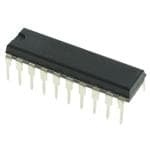
ICGOO电子元器件商城为您提供AD7528JNZ由Analog设计生产,在icgoo商城现货销售,并且可以通过原厂、代理商等渠道进行代购。 AD7528JNZ价格参考¥95.54-¥120.69。AnalogAD7528JNZ封装/规格:数据采集 - 数模转换器, 8 位 数模转换器 2 20-PDIP。您可以下载AD7528JNZ参考资料、Datasheet数据手册功能说明书,资料中有AD7528JNZ 详细功能的应用电路图电压和使用方法及教程。
AD7528JNZ是由Analog Devices Inc.(ADI公司)生产的一款双通道8位数模转换器(DAC),属于数据采集系统中的数模转换器类别。其主要应用场景包括但不限于以下领域:

1. 工业自动化与控制:
   AD7528JNZ可用于工业自动化系统中,例如过程控制、电机控制和传感器信号调节等。它能够将数字信号转换为模拟信号,用于驱动执行器、阀门或电机控制器,实现精确的输出控制。

2. 通信设备:
   在通信系统中,AD7528JNZ可以用来生成调制信号或基准电压,适用于低频信号处理任务,如音频信号生成或调制解调器设计。

3. 测试与测量仪器:
   该器件适合用于测试设备中,例如信号发生器、示波器校准模块或数据记录仪。通过提供高精度的模拟输出,确保测试结果的准确性。

4. 消费电子与音频设备:
   AD7528JNZ可应用于简单的音频信号合成或音量控制电路中,为低成本音频设备提供基础功能支持。

5. 医疗设备:
   在一些医疗应用中,如便携式监护仪或超声波设备,AD7528JNZ可用于生成激励信号或控制模拟前端电路。

6. 汽车电子:
   该DAC可以用于汽车控制系统中,例如温度调节、灯光亮度控制或其他需要模拟信号输出的功能模块。

AD7528JNZ具有双通道独立DAC、三态输入缓冲器以及兼容TTL/CMOS的接口,使其在多路信号处理场景下表现出色。此外,其单电源供电特性简化了设计复杂度,非常适合对成本敏感且要求性能稳定的嵌入式系统。
| 参数 | 数值 |
| 产品目录 | 集成电路 (IC)半导体 |
| 描述 | IC DAC 8BIT DUAL MULTIPLY 20-DIP数模转换器- DAC CMOS 8-Bit Buffered Multiplying |
| 产品分类 | |
| 品牌 | Analog Devices Inc |
| 产品手册 | |
| 产品图片 |
|
| rohs | 符合RoHS无铅 / 符合限制有害物质指令(RoHS)规范要求 |
| 产品系列 | 数据转换器IC,数模转换器- DAC,Analog Devices AD7528JNZ- |
| 数据手册 | |
| 产品型号 | AD7528JNZ |
| 产品培训模块 | http://www.digikey.cn/PTM/IndividualPTM.page?site=cn&lang=zhs&ptm=19145http://www.digikey.cn/PTM/IndividualPTM.page?site=cn&lang=zhs&ptm=18614http://www.digikey.cn/PTM/IndividualPTM.page?site=cn&lang=zhs&ptm=26125http://www.digikey.cn/PTM/IndividualPTM.page?site=cn&lang=zhs&ptm=26140http://www.digikey.cn/PTM/IndividualPTM.page?site=cn&lang=zhs&ptm=26150http://www.digikey.cn/PTM/IndividualPTM.page?site=cn&lang=zhs&ptm=26147 |
| 产品目录页面 | |
| 产品种类 | 数模转换器- DAC |
| 位数 | 8 |
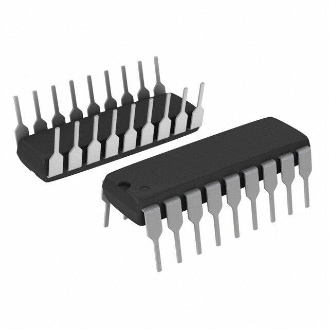
| 供应商器件封装 | 20-PDIP |
| 分辨率 | 8 bit |
| 包装 | 管件 |
| 商标 | Analog Devices |
| 安装类型 | 通孔 |
| 安装风格 | Through Hole |
| 封装 | Tube |
| 封装/外壳 | 20-DIP(0.300",7.62mm) |
| 封装/箱体 | PDIP-20 |
| 工作温度 | -40°C ~ 85°C |
| 工厂包装数量 | 18 |
| 建立时间 | - |
| 接口类型 | Parallel |
| 数据接口 | 并联 |
| 最大功率耗散 | 30 mW |
| 最大工作温度 | + 125 C |
| 最小工作温度 | - 55 C |
| 标准包装 | 18 |
| 电压参考 | External |
| 电压源 | 单电源 |
| 电源电压-最大 | 15 V |
| 电源电压-最小 | 5 V |
| 积分非线性 | +/- 1 LSB |
| 稳定时间 | 180 ns |
| 系列 | AD7528 |
| 结构 | R-2R |
| 转换器数 | 2 |
| 转换器数量 | 2 |
| 输出数和类型 | 2 电流,单极2 电流,双极 |
| 输出类型 | Current |
| 采样比 | 5.6 MSPs |
| 采样率(每秒) | - |


- 商务部:美国ITC正式对集成电路等产品启动337调查
- 曝三星4nm工艺存在良率问题 高通将骁龙8 Gen1或转产台积电
- 太阳诱电将投资9.5亿元在常州建新厂生产MLCC 预计2023年完工
- 英特尔发布欧洲新工厂建设计划 深化IDM 2.0 战略
- 台积电先进制程称霸业界 有大客户加持明年业绩稳了
- 达到5530亿美元!SIA预计今年全球半导体销售额将创下新高
- 英特尔拟将自动驾驶子公司Mobileye上市 估值或超500亿美元
- 三星加码芯片和SET,合并消费电子和移动部门,撤换高东真等 CEO
- 三星电子宣布重大人事变动 还合并消费电子和移动部门
- 海关总署:前11个月进口集成电路产品价值2.52万亿元 增长14.8%


PDF Datasheet 数据手册内容提取
a CMOS Dual 8-Bit Buffered Multiplying DAC AD7528 FEATURES FUNCTIONAL BLOCK DIAGRAM On-Chip Latches for Both DACs +5 V to +15 V Operation VREFA DACs Matched to 1% VDD RFB A Four Quadrant Multiplication DB0 TTL/CMOS Compatible DATA INPUT LATCH DAC A OUT A Latch Free (Protection Schottkys not Required) INPUTS BUFFER DB7 APPLICATIONS AGND Digital Control of: DAC A/ AD7528 GFialtienr/ APtatreanmueatteiorsn DACC BS COLONTGRICOL RFB B Stereo Audio Circuits WR OUT B LATCH DAC B X-Y Graphics DGND VREFB GENERAL DESCRIPTION ORDERING GUIDE1 The AD7528 is a monolithic dual 8-bit digital/analog converter featuring excellent DAC-to-DAC matching. It is available in Temperature Relative Gain Package Model2 Ranges Accuracy Error Options3 skinny 0.3" wide 20-lead DIPs and in 20-lead surface mount packages. AD7528JN –40(cid:176) C to +85(cid:176) C – 1 LSB – 4 LSB N-20 AD7528KN –40(cid:176) C to +85(cid:176) C – 1/2 LSB – 2 LSB N-20 Separate on-chip latches are provided for each DAC to allow AD7528LN –40(cid:176) C to +85(cid:176) C – 1/2 LSB – 1 LSB N-20 easy microprocessor interface. AD7528JP –40(cid:176) C to +85(cid:176) C – 1 LSB – 4 LSB P-20A Data is transferred into either of the two DAC data latches via a AD7528KP –40(cid:176) C to +85(cid:176) C – 1/2 LSB – 2 LSB P-20A common 8-bit TTL/CMOS compatible input port. Control AD7528LP –40(cid:176) C to +85(cid:176) C – 1/2 LSB – 1 LSB P-20A input DAC A/DAC B determines which DAC is to be loaded. AD7528JR –40(cid:176) C to +85(cid:176) C – 1 LSB – 4 LSB R-20 The AD7528’s load cycle is similar to the write cycle of a ran- AD7528KR –40(cid:176) C to +85(cid:176) C – 1/2 LSB – 2 LSB R-20 AD7528LR –40(cid:176) C to +85(cid:176) C – 1/2 LSB – 1 LSB R-20 dom access memory and the device is bus compatible with most AD7528AQ –40(cid:176) C to +85(cid:176) C – 1 LSB – 4 LSB Q-20 8-bit microprocessors, including 6800, 8080, 8085, Z80. AD7528BQ –40(cid:176) C to +85(cid:176) C – 1/2 LSB – 2 LSB Q-20 The device operates from a +5 V to +15 V power supply, dis- AD7528CQ –40(cid:176) C to +85(cid:176) C – 1/2 LSB – 1 LSB Q-20 sipating only 20 mW of power. AD7528SQ –55(cid:176) C to +125(cid:176) C – 1 LSB – 4 LSB Q-20 AD7528TQ –55(cid:176) C to +125(cid:176) C – 1/2 LSB – 2 LSB Q-20 Both DACs offer excellent four quadrant multiplication charac- AD7528UQ –55(cid:176) C to +125(cid:176) C – 1/2 LSB – 1 LSB Q-20 teristics with a separate reference input and feedback resistor for each DAC. NOTES 1Analog Devices reserves the right to ship side-brazed ceramic in lieu of cerdip. Parts will be marked with cerdip designator “Q.” PRODUCT HIGHLIGHTS 2Processing to MIL-STD-883C, Class B is available. To order, add suffix “/883B” to 1. DAC-to-DAC matching: since both of the AD7528 DACs are part number. For further information, see Analog Devices’ 1990 Military Products fabricated at the same time on the same chip, precise match- Databook. 3N = Plastic DIP; P = Plastic Leaded Chip Carrier; Q = Cerdip; R = SOIC. ing and tracking between DAC A and DAC B is inherent. The AD7528’s matched CMOS DACs make a whole new range of applications circuits possible, particularly in the audio, graphics and process control areas. 2. Small package size: combining the inputs to the on-chip DAC latches into a common data bus and adding a DAC A/DAC B select line has allowed the AD7528 to be packaged in either a small 20-lead DIP, SOIC or PLCC. REV.B Information furnished by Analog Devices is believed to be accurate and reliable. However, no responsibility is assumed by Analog Devices for its use, nor for any infringements of patents or other rights of third parties One Technology Way, P.O. Box 9106, Norwood, MA 02062-9106, U.S.A. which may result from its use. No license is granted by implication or Tel: 781/329-4700 World Wide Web Site: http://www.analog.com otherwise under any patent or patent rights of Analog Devices. Fax: 781/326-8703 © Analog Devices, Inc., 1998
AD7528–SPECIFICATIONS (V A = V B = +10 V; OUT A = OUT B = O V unless otherwise noted) REF REF VDD = +5 V VDD = +15 V Parameter Version1 TA = +25(cid:176)C TMIN, TMAX TA= +25(cid:176)C TMIN, TMAX Units Test Conditions/Comments STATIC PERFORMANCE2 Resolution All 8 8 8 8 Bits Relative Accuracy J, A, S – 1 – 1 – 1 – 1 LSB max This is an Endpoint Linearity Specification K, B, T – 1/2 – 1/2 – 1/2 – 1/2 LSB max L, C, U – 1/2 – 1/2 – 1/2 – 1/2 LSB max Differential Nonlinearity All – 1 – 1 – 1 – 1 LSB max All Grades Guaranteed Monotonic Over Full Operating Temperature Range Gain Error J, A, S – 4 – 6 – 4 – 5 LSB max Measured Using Internal RFB A and RFB B K, B, T – 2 – 4 – 2 – 3 LSB max Both DAC Latches Loaded with 11111111 L, C, U – 1 – 3 – 1 – 1 LSB max Gain Error is Adjustable Using Circuits of Figures 4 and 5 Gain Temperature Coefficient3 D Gain/D Temperature All – 0.007 – 0.007 – 0.0035 – 0.0035 %/(cid:176)C max Output Leakage Current OUT A (Pin 2) All – 50 – 400 – 50 – 200 nA max DAC Latches Loaded with 00000000 OUT B (Pin 20) All – 50 – 400 – 50 – 200 nA max Input Resistance (VREF A, VREF B) All 8 8 8 8 kW min Input Resistance TC = –300 ppm/(cid:176)C, Typical 15 15 15 15 kW max Input Resistance is 11 kW VREF A/VREF B Input Resistance Match All – 1 – 1 – 1 – 1 % max DIGITAL INPUTS4 Input High Voltage V All 2.4 2.4 13.5 13.5 V min IH Input Low Voltage V All 0.8 0.8 1.5 1.5 V max IL Input Current I All – 1 – 10 – 1 – 10 m A max V = 0 or V IN IN DD Input Capacitance DB0–DB7 All 10 10 10 10 pF max WR, CS, DAC A/DAC B All 15 15 15 15 pF max SWITCHING CHARACTERISTICS3 See Timing Diagram Chip Select to Write Set Up Time tCS All 90 100 60 80 ns min Chip Select to Write Hold Time tCH All 0 0 10 15 ns min DAC Select to Write Set Up Time tAS All 90 100 60 80 ns min DAC Select to Write Hold Time t All 0 0 10 15 ns min AH Data Valid to Write Set Up Time t All 80 90 30 40 ns min DS Data Valid to Write Hold Time t All 0 0 0 0 ns min DH Write Pulsewidth t All 90 100 60 80 ns min WR POWER SUPPLY See Figure 3 IDD All 2 2 2 2 mA max All Digital Inputs VIL or VIH All 100 500 100 500 m A max All Digital Inputs 0 V or VDD AC PERFORMANCE CHARACTERISTICS5 (Measured Using Recommended P.C. Board Layout (Figure 7) and AD644 as Output Amplifiers) V = +5 V V = +15 V DD DD Parameter Version1 T = +25(cid:176)C T , T T = +25(cid:176)C T , T Units Test Conditions/Comments A MIN MAX A MIN MAX DC SUPPLY REJECTION (D GAIN/D VDD) All 0.02 0.04 0.01 0.02 % per % max D VDD = – 5% CURRENT SETTLING TIME2 All 350 400 180 200 ns max To 1/2 LSB. OUT A/OUT B Load = 100 W . WR = CS = 0 V. DB0–DB7 = 0 V to VDD or VDD to 0 V PROPAGATION DELAY (From Digital In- V A = V B = +10 V REF REF put to 90% of Final Analog Output Current) All 220 270 80 100 ns max OUT A, OUT B Load = 100 W C = 13 pF EXT WR = CS = 0 V DB0–DB7 = 0 V to V or DD V to 0 V DD DIGITAL-TO-ANALOG GLITCH IMPULSE All 160 440 nV sec typ For Code Transition 00000000 to 11111111 OUTPUT CAPACITANCE COUTA All 50 50 50 50 pF max DAC Latches Loaded with 00000000 COUTB 50 50 50 50 pF max COUTA 120 120 120 120 pF max DAC Latches Loaded with 11111111 COUTB 120 120 120 120 pF max AC FEEDTHROUGH6 VREF A to OUT A All –70 –65 –70 –65 dB max VREF A, VREF B = 20 V p-p Sine Wave VREF B to OUT B –70 –65 –70 –65 dB max @ 100 kHz –2– REV. B
AD7528 VDD = +5 V VDD = +15 V Parameter Version1 TA = +25(cid:176)C TMIN, TMAX TA= +25(cid:176)C TMIN, TMAX Units Test Conditions/Comments CHANNEL-TO-CHANNEL ISOLATION Both DAC Latches Loaded with 11111111. VREF A to OUT B All –77 –77 dB typ VREF A = 20 V p-p Sine Wave @ 100 kHz VREF B = 0 V see Figure 6. VREF B to OUT A –77 –77 dB typ VREF A = 20 V p-p Sine Wave @ 100 kHz VREF A = 0 V see Figure 6. DIGITAL CROSSTALK All 30 60 nV sec typ Measured for Code Transition 00000000 to 11111111 HARMONIC DISTORTlON All –85 –85 dB typ VIN = 6 V rms @ 1 kHz NOTES 1Temperature Ranges areJ, K, L Versions: –40(cid:176)C to +85(cid:176)C A, B, C Versions: –40(cid:176)C to +85(cid:176)C AD7528, ideal maximum output is V – 1 LSB. Gain error of REF S, T, U Versions: –55(cid:176)C to +125(cid:176)C both DACs is adjustable to zero with external resistance. 2Specifications applies to both DACs in AD7528. 3Guaranteed by design but not production tested. Output Capacitance 4Logic inputs are MOS Gates. Typical input current (+25(cid:176)C) is less than 1 nA. Capacitance from OUT A or OUT B to AGND. 5These characteristics are for design guidance only and are not subject to test. 6Feedthrough can be further reduced by connecting the metal lid on the ceramic package Digital to Analog Glitch lmpulse (suffix D) to DGND. The amount of charge injected from the digital inputs to the Specifications subject to change without notice. analog output when the inputs change state. This is normally ABSOLUTE MAXIMUM RATINGS specified as the area of the glitch in either pA-secs or nV-secs (T = +25(cid:176)C unless otherwise noted) A depending upon whether the glitch is measured as a current or V to AGND . . . . . . . . . . . . . . . . . . . . . . . . . . . . 0 V, +17 V DD voltage signal. Glitch impulse is measured with V A, V to DGND . . . . . . . . . . . . . . . . . . . . . . . . . . . . 0 V, +17 V REF DD V B = AGND. AGND to DGND . . . . . . . . . . . . . . . . . . . . . . . . V + 0.3 V REF DD Propagation Delay DGND to AGND . . . . . . . . . . . . . . . . . . . . . . . . V + 0.3 V DD This is a measure of the internal delays of the circuit and is Digital Input Voltage to DGND . . . . . . .–0.3 V, V + 0.3 V DD defined as the time from a digital input change to the analog V , V to AGND . . . . . . . . . . . . . .–0.3 V, V + 0.3 V PIN2 PIN20 DD V A, V B to AGND . . . . . . . . . . . . . . . . . . . . . . .– 25 V output current reaching 90% of its final value. REF REF V A, V B to AGND . . . . . . . . . . . . . . . . . . . . . . .– 25 V Channel-to-Channel Isolation RFB RFB Power Dissipation (Any Package) to +75(cid:176) C . . . . . . . 450 mW The proportion of input signal from one DAC’s reference input Derates above +75(cid:176) C by . . . . . . . . . . . . . . . . . . . 6 mW/(cid:176) C which appears at the output of the other DAC, expressed as a Operating Temperature Range ratio in dB. Commercial (J, K, L) Grades . . . . . . . . . . . –40(cid:176) C to +85(cid:176) C Digital Crosstalk Industrial (A, B, C) Grades . . . . . . . . . . . . –40(cid:176) C to +85(cid:176) C The glitch energy transferred to the output of one converter due Extended (S, T, U) Grades . . . . . . . . . . . –55(cid:176) C to +125(cid:176) C to a change in digital input code to the other converter. Speci- Storage Temperature . . . . . . . . . . . . . . . . . . –65(cid:176) C to +150(cid:176) C fied in nV secs. Lead Temperature (Soldering, 10 secs) . . . . . . . . . . . .+300(cid:176) C PIN CONFIGURATIONS CAUTION: 1. ESD sensitive device. The digital control inputs are diode PLCC protected; however, permanent damage may occur on uncon- nUencutesded d deveivciecse ss umbujesct tbeed sttoo rheigdh i ne nceorngdyu eclteicvter ofostaamti co fri eslhdusn.ts. R AFB OUT A AGND OUT B R BFB 3 2 1 20 19 2. Do not insert this device into powered sockets. Remove power before insertion or removal. VREF A 4 PIDINE N1TIFIER 18 VREF B DGND 5 17 VDD AD7528 TERMINOLOGY DAC A/DAC B 6 TOP VIEW 16 WR Relative Accuracy (MSB) DB7 7 (Not to Scale) 15 CS Relative accuracy or endpoint nonlinearity is a measure of the DB6 8 14 DB0 (LSB) maximum deviation from a straight line passing through the 9 10 11 12 13 DIP, SOIC endpoints of the DAC transfer function. It is measured after 5 4 3 2 1 B B B B B D D D D D adjusting for zero and full scale and is normally expressed in AGND 1 20 OUT B LSBs or as a percentage of full scale reading. OUT A 2 19 RFB B Differential Nonlinearity RFB A 3 18 VREF B Differential nonlinearity is the difference between the measured VREF A 4 17 VDD change and the ideal 1 LSB change between any two adjacent DGND 5 AD7528 16 WR codes. A specified differential nonlinearity of – 1 LSB max over DAC A/DAC B 6 TOP VIEW 15 CS the operating temperature range ensures monotonicity. (Not to Scale) (MSB) DB7 7 14 DB0 (LSB) Gain Error DB6 8 13 DB1 Gain error or full-scale error is a measure of the output error DB5 9 12 DB2 between an ideal DAC and the actual device output. For the DB4 10 11 DB3 REV. B –3–
AD7528 INTERFACE LOGIC INFORMATION Figure 1. An inverted R-2R ladder structure is used, that is, bi- DAC Selection: nary weighted currents are switched between the DAC output Both DAC latches share a common 8-bit input port. The con- and AGND thus maintaining fixed currents in each ladder leg trol input DAC A/DAC B selects which DAC can accept data independent of switch state. from the input port. EQUIVALENT CIRCUIT ANALYSIS Mode Selection: Figure 2 shows an approximate equivalent circuit for one of the Inputs CS and WR control the operating mode of the selected AD7528’s D/A converters, in this case DAC A. A similar DAC. See Mode Selection Table below. equivalent circuit can be drawn for DAC B. Note that AGND Write Mode: (Pin 1) is common for both DAC A and DAC B. When CS and WR are both low the selected DAC is in the write The current source I is composed of surface and junc- mode. The input data latches of the selected DAC are transpar- LEAKAGE tion leakages and, as with most semiconductor devices, approxi- ent and its analog output responds to activity on DB0–DB7. mately doubles every 10(cid:176) C. The resistor R as shown in Figure O Hold Mode: 2 is the equivalent output resistance of the device which varies The selected DAC latch retains the data which was present on with input code (excluding all 0s code) from 0.8 R to 2 R. R is DB0–DB7 just prior to CS or WR assuming a high state. Both typically 11 kW . C is the capacitance due to the N-channel OUT analog outputs remain at the values corresponding to the data in switches and varies from about 50 pF to 120 pF depending their respective latches. upon the digital input. g(V A, N) is the Thevenin equivalent REF Mode Selection Table voltage generator due to the reference input voltage V A and REF the transfer function of the R-2R ladder. DAC A/DAC B CS WR DAC A DAC B L L L WRITE HOLD R H L L HOLD WRITE RO RFB A X H X HOLD HOLD OUT A X X H HOLD HOLD g(VREF A, N) ILKG COUT AGND L = Low State; H = High State; X = Don’t Care. Figure 2.Equivalent Analog Output Circuit of DAC A WRITE CYCLE TIMING DIAGRAM CIRCUIT INFORMATION–DIGITAL SECTION t tCS CH VDD The input buffers are simple CMOS inverters designed such CHIP SELECT that when the AD7528 is operated with V = 5 V, the buffer 0 DD t converts TTL input levels (2.4 V and 0.8 V) into CMOS logic tAS AH VDD levels. When V is in the region of 2.0 volts to 3.5 volts the DAC A/DAC B IN 0 input buffers operate in their linear region and pass a quiescent tWR VDD current, see Figure 3. To minimize power supply currents it is WRITE 0 recommended that the digital input voltages be as close to the t DS t supply rails (V and DGND) as is practically possible. DH DD (DBD0 A– TDAB I7N) VVIILH DATA IN STABLE 0VDD Trahneg eA 5D £7 5V28 m £ a 1y5 b veo oltpse. rWatietdh wVith a=n +y 1s5u pVp ltyh ev oinltpaguet liong tihce NOTES: DD DD 1. ALL INPUT SIGNAL RISE AND FALL TIMES MEASURED levels are CMOS compatible only, i.e., 1.5 V and 13.5 V. FROM 10% TO 90% OF VDD. VDD = +5V, tr = tf = 20ns; 2 . TVIDMDI N= G+ 1M5EVA, tSr U=R tEf M= E4N0nTs R;EFERENCE LEVEL ISVIH + VIL 9 2 800 VDD = +15V TA = +258C 8 CIRCUIT INFORMATION—D/A SECTION 700 ALL DIGITAL INPUTS 7 Tvsinteahgrbet sel weArs iDt,th cD7ihn5Ae 2fsCi.8l m AAc o sRanim-nt2adpRi nlD isfla iAtedwdCd o eDB rid /.Aa eEn ncdatic irechcia ugDl hit8At - fNboCri- t c cDmohAnausnClitnsi tpAesll yoicisfun srgahr ehDoniwg/tAhn s l tcyienoenr-- mI A (V = +5V)DDDD654320000000000 VDD = +5V TIED TOGETHER 65432I mA (V = +15V)DDDD R R R VREF A 100 1 2R 2R 2R 2R 2R S1 S2 S3 S8 R 0 1 2 3 4 5 6 7 8 9 10 11 12 13 14 RFB A VIN – Volts OUT A AGND Figure 3.Typical Plots of Supply Current, IDD vs. Logic DAC A DATA LATCHES Input Voltage VIN, for VDD = +5 V and +15 V AND DRIVERS Figure 1.Simplified Functional Circuit for DAC A –4– REV. B
AD7528 VIN A (± 10V) Table I. Unipolar Binary Code Table R11 DAC Latch Contents Analog Output R21 MSB LSB (DAC A or DAC B) VDD RFB A C12 (cid:230) 255(cid:246) INDPAUTTDASB0 BIUNFPFUETR LATCH DAC A OUT A VOUT A 1 1 1 1 1 1 1 1 – VINŁ(cid:231) 256ł(cid:247) DB7 (cid:230) 129(cid:246) AGND AGND 1 0 0 0 0 0 0 1 –VINŁ(cid:231) 256ł(cid:247) DDAACC A B/ AD7528 R41 1 0 0 0 0 0 0 0 –VIN(cid:230)Ł(cid:231) 122586(cid:246)ł(cid:247) =- V2IN CS COLONTGRICOL RFB B C22 (cid:230) 127(cid:246) WR LATCH DAC B OUT B VOUT B 0 1 1 1 1 1 1 1 –VINŁ(cid:231) 256ł(cid:247) DGND (cid:230) 1 (cid:246) AGND 0 0 0 0 0 0 0 1 –VINŁ(cid:231) 256ł(cid:247) R31 (cid:230) 0 (cid:246) VIN B 0 0 0 0 0 0 0 0 –VINŁ(cid:231) 256ł(cid:247) =0 (± 10V) NOTES: 1R1, R2 AND R3, R4 USED ONLY IF GAIN ADJUSTMENT IS REQUIRED. Note: 1 LSB = (2-8)(V )= 1 (V ) 2 CS1E,E C T2A PBHLAES IEII FCOORM PREENCSOAMTMIOENN D(1E0Dp FV–A1L5UpFE)S I.S REQUIRED WHEN IN 256 IN USING HIGH SPEED AMPLIFIERS TO PREVENT RINGING OR OSCILLATION. Figure 4.Dual DAC Unipolar Binary Operation (2 Quadrant Multiplication); See Table I VIN A Table II. Bipolar (Offset Binary) Code Table (± 10V) R5 20kV DAC Latch Contents Analog Output R62 R11 20kV MSB LSB (DAC A or DAC B) VDDDB0 RFBR A21 C1130Rk7V2 5Rk1V1A2 VOUT A 1 1 1 1 1 1 1 1 + VIN(cid:230)Ł(cid:231) 112287(cid:246)ł(cid:247) INDPAUTTAS BIUNFPFUETR LATCH DAC A OUT A A1 AGND 1 0 0 0 0 0 0 1 DB7 AGND 1 0 0 0 0 0 0 0 0 AGND DAC A/ AD7528 R41 (cid:230) 1 (cid:246) DACC BS COLONTGRICOL RFB B C23 0 1 1 1 1 1 1 1 – VINŁ(cid:231) 128ł(cid:247) DGWNDR LATCH DAC B OAUGT NBD A130Rk9V2 20Rk8V 0 0 0 0 0 0 0 1 – VIN(cid:230)Ł(cid:231) 112287(cid:246)ł(cid:247) (cid:230) 128(cid:246) R31 2R01k0V2 A4 VOUT B 0 0 0 0 0 0 0 0 – VINŁ(cid:231) 128ł(cid:247) VIN B 5Rk1V2 Note: 1 LSB = ( 2-7)(VIN)=1218(VIN) (± 10V) AGND NOTES: 1R1, R2 AND R3, R4 USED ONLY IF GAIN ADJUSTMENT IS REQUIRED. SEE TABLE III FOR RECOMMENDED VALUES. ADJUST R1 FOR VOUT A = 0V WITH CODE 10000000 IN DAC A LATCH. ADJUST R3 FOR VOUT B = 0V WITH CODE 10000000 IN DAC B LATCH. 2MATCHING AND TRACKING IS ESSENTIAL FOR RESISTOR PAIRS Table III. Recommended Trim Resistor R6, R7 AND R9, R10. Values vs. Grade 3C1, C2 PHASE COMPENSATION (10pF–15pF) MAY BE REQUIRED IF A1/A3 IS A HIGH SPEED AMPLIFIER. Trim Figure 5.Dual DAC Bipolar Operation Resistor J/A/S K/B/T L/C/U (4 Quadrant Multiplication); See Table II R1; R3 1 k 500 200 R2; R4 330 150 82 REV. B –5–
AD7528 APPLICATIONS INFORMATION ship between input frequency and channel to channel isolation. Application Hints Figure 7 shows a printed circuit layout for the AD7528 and the To ensure system performance consistent with AD7528 specifi- AD644 dual op amp which minimizes feedthrough and crosstalk. cations, careful attention must be given to the following points: SINGLE SUPPLY APPLICATIONS 1. GENERAL GROUND MANAGEMENT: AC or transient The AD7528 DAC R-2R ladder termination resistors are con- voltages between the AD7528 AGND and DGND can cause nected to AGND within the device. This arrangement is par- noise injection into the analog output. The simplest method ticularly convenient for single supply operation because AGND of ensuring that voltages at AGND and DGND are equal is may be biased at any voltage between DGND and V . Figure DD to tie AGND and DGND together at the AD7528. In more 8 shows a circuit which provides two +5 V to +8 V analog out- complex systems where the AGND–DGND intertie is on the puts by biasing AGND +5 V up from DGND. The two DAC backplane, it is recommended that diodes be connected in reference inputs are tied together and a reference input voltage inverse parallel between the AD7528 AGND and DGND is obtained without a buffer amplifier by making use of the pins (1N914 or equivalent). constant and matched impedances of the DAC A and DAC B 2. OUTPUT AMPLIFIER OFFSET: CMOS DACs exhibit a reference inputs. Current flows through the two DAC R-2R code-dependent output resistance which in turn causes a ladders into R1 and R1 is adjusted until the V A and V B REF REF code-dependent amplifier noise gain. The effect is a code- inputs are at +2 V. The two analog output voltages range from dependent differential nonlinearity term at the amplifier +5 V to +8 V for DAC codes 00000000 to 11111111. output which depends on V (V is amplifier input offset voltage). This differential noOnSlineOaSrity term adds to the R/2R VDD = +15V differential nonlinearity. To maintain monotonic operation, it is recommended that amplifier VOS be no greater than 10% of DAC A VOUT A = +5V TO +8V 1 LSB over the temperature range of interest. DATA DB0 INPUTS DB7 SUGGESTED 3. HIGH FREQUENCY CONSIDERATIONS: The output CS AD7528 OP AMP: AD644 capacitance of a CMOS DAC works in conjunction with the WR amplifier feedback resistance to add a pole to the open loop DAC A/DAC B DAC B VOUT B = +5V TO +8V response. This can cause ringing or oscillation. Stability can 2 VOLTS be restored by adding a phase compensation capacitor in 10kRV1 parallel with the feedback resistor. R2 AD584J VDD 1kV DYNAMIC PERFORMANCE GND The dynamic performance of the two DACs in the AD7528 will Figure 8.AD7528 Single Supply Operation depend upon the gain and phase characteristics of the output Figure 9 shows DAC A of the AD7528 connected in a positive amplifiers together with the optimum choice of the PC board reference, voltage switching mode. This configuration is useful layout and decoupling components. Figure 6 shows the relation in that V is the same polarity as V allowing single supply OUT IN operation. However, to retain specified linearity, V must be in IN –100 the range 0 V to +2.5 V and the output buffered or loaded with TA = +258C a high impedance, see Figure 10. Note that the input voltage is dB–90 VVDIND = = 2 +01V5 PVEAK TO PEAK connected to the DAC OUT A and the output voltage is taken N – –80 from the DAC VREF A pin. O OLATI–70 VIN (0V TO +2.5V) VREF A VOUT S–60 I –50 VDD DAC A OUT A +15V 20k 50k 100k 200k 500k 1M AD7528 INPUT FREQUENCY – Hz Figure 9.AD7528 in Single Supply, Voltage Switching Mode Figure 6.Channel-to-Channel Isolation 3 PIN 8 OF TO-5 CAN (AD644) AD644 V+ TA = +258C VDD = +15V B 2 V– LS AGND AD7528 PIN 1 R – NONLINEARITY O C1 LOCATION RR VREF B* C2 LOCATION * INNOPTUET SCREENS E 1 VDD VREF A* TO REDUCE DIFFERENTIAL WR DGND FEEDTHROUGH. NONLINEARITY LAYOUT SHOWS CS AD7528 DAC A/DAC B COPPER SIDE LSB MSB (i.e., BOTTOM VIEW). 2.5 3 3.5 4 4.5 5 5.5 6 6.5 7 7.5 Figure 7.Suggested PC Board Layout for AD7528 with VINA – Volts AD644 Dual Op Amp Figure 10.Typical AD7528 Performance in Single Supply Voltage Switching Mode (K/B/T, L/C/U Grades) –6– REV. B
AD7528 MICROPROCESSOR INTERFACE A8–A15 ADDRESS BUS A0–A15 ADDRESS BUS CPU ADDRESS A** DAC A/DAC B A** 8085 DLEOCGOIDCE CS DAC A VMA ADDLEDOCRGOEIDCSES CDSAC A/DDAACC B A WR A + 1** WR AD7528* C68P0Uf02 A + 1** WR AD7528* ALE L8A2T1C2H DDBB07 DAC B DB0 DAC B DB7 AD0–AD7 ADDR/DATA BUS *ANALOG CIRCUITRY HAS BEEN OMITTED FOR CLARITY D0–D7 **A = DECODED 7528 ADDR DAC A DATA BUS A + 1 = DECODED 7528 ADDR DAC B *ANALOG CIRCUITRY HAS BEEN OMITTED FOR CLARITY NOTE: **A = DECODED 7528 ADDR DAC A 8085 INSTRUCTION SHLD (STORE H & L DIRECT) CAN UPDATE A + 1 = DECODED 7528 ADDR DAC B BOTH DACs WITH DATA FROM H AND L REGISTERS Figure 11.AD7528 Dual DAC to 6800 CPU Interface Figure 12.AD7528 Dual DAC to 8085 CPU Interface PROGRAMMABLE WINDOW COMPARATOR In the circuit of Figure 13 the AD7528 is used to implement a T0E TSOT –INVPRUEFT VREF A RFB A VDD OUT A 3 7 1kVVCC pwrerisotphge rtcahtmiev merelayqb.u lIiefr etwdhi enu dtpeopswte r ic naopnmudtp liaosrw anetoort r v.w oDiltthAaigCne s tl hiAme aiptnsr dofg oBrra tamhreem tleoedsatd,ed DAC A 2 DATA DB0 limits, the pass/fail output will indicate a fail (logic zero). INPUTS DB7 AD311 CS AD7528 COMPARATOR PASS/FAIL WR OUTPUT OUT B 2 DAC A/DAC B 7 DAC B 3 +VREF VREF B AD311 RFB B COMPARATOR Figure 13.Digitally Programmable Window Comparator (Upper and Lower Limit Detector) PROGRAMMABLE STATE VARIABLE FILTER In this state variable or universal filter configuration (Figure 14) The filter provides low pass, high pass and band pass outputs DACs A1 and B1 control the gain and Q of the filter character- and is ideally suited for applications where microprocessor istic while DACs A2 and B2 control the cutoff frequency, f . control of filter parameters is required, e.g., equalizer, tone C DACs A2 and B2 must track accurately for the simple expres- controls, etc. sion for f to hold. This is readily accomplished by the AD7528. C Programmable range for component values shown is f = 0 kHz Op amps are 2 · AD644. C3 compensates for the effects of op C to 15 kHz and Q = 0.3 to 4.5. amp gain bandwidth limitations. R5 CIRCUIT EQUATIONS 30kV C1=C2,R1=R2,R4=R5 R4 C1 C2 30kV C3 1000pF 1000pF R3 47pF 10kV 1 A1 A2 HPAIGSHS A3 A4 LPOASWS fC =2p R1C1 OUTPUT OUTPUT BPAASNSD Q=R3· RF VDD VDD OUTPUT R4 RFBB1 AD7528 R A =– F VIN DARCS A1 DARCF B1 DARC1 A2 AD7528 DARC2 B2 O RS NOTE DAC Equivalent Resistance DB0–DB7 DB0–DB7 Equals DATA 1 CS WR DAC A/DAC B DATA 2 CS WR DAC A/DAC B 256· (DACLadderResistance) Figure 14.Digitally Controlled State Variable Filter DACDigitalCode REV. B –7–
AD7528 DIGITALLY CONTROLLED DUAL TELEPHONE ATTENUATOR Table IV. Attenuation vs. DAC A, DAC B Code for the Circuit In this configuration the AD7528 functions as a 2-channel digi- of Figure 15 tally controlled attenuator. Ideal for stereo audio and telephone signal level control applications. Table IV gives input codes vs. Attn. DAC Input Code In Attn. DAC Input Code In attenuation for a 0 dB to 15.5 dB range. dB Code Decimal dB Code Decimal Input Code = 256 3 10 exp (cid:230)(cid:231) - Attenuation, dB(cid:246)(cid:247) 00..05 11 11 11 11 10 10 11 10 225452 8888..50 00 11 11 00 00 01 01 00 19062 9/98 Ł 20 ł – 1.0 1 1 1 0 0 1 0 0 228 89.0 0 1 0 1 1 0 1 1 91 0 – 1.5 1 1 0 1 0 1 1 1 215 89.5 0 1 0 1 0 1 1 0 86 1e 8 2.0 1 1 0 0 1 0 1 1 203 10.0 0 1 0 1 0 0 0 1 81 6 VDD 2.5 1 1 0 0 0 0 0 0 192 10.5 0 1 0 0 1 1 0 0 76 C VIN A DAC A A1 VOUT A 3.0 1 0 1 1 0 1 0 1 181 11.0 0 1 0 0 1 0 0 0 72 3.5 1 0 1 0 1 0 1 1 171 11.5 0 1 0 0 0 1 0 0 68 4.0 1 0 1 0 0 0 1 0 162 12.0 0 1 0 0 0 0 0 0 64 DB0 DATA BUS 4.5 1 0 0 1 1 0 0 0 152 12.5 0 0 1 1 1 1 0 1 61 DB7 CS 5.0 1 0 0 1 0 0 0 0 144 13.0 0 0 1 1 1 0 0 1 57 AD7528 WR 5.5 1 0 0 0 1 0 0 0 136 13.5 0 0 1 1 0 1 1 0 54 DAC A/DAC B 6.0 1 0 0 0 0 0 0 0 128 14.0 0 0 1 1 0 0 1 1 51 VOUT B A2 DAC B VIN B 67..50 00 11 11 11 10 00 01 10 112114 1145..50 00 00 11 10 01 01 01 00 4486 7.5 0 1 1 0 1 1 0 0 108 15.5 0 0 1 0 1 0 1 1 43 SUGGESTED OP AMP: AD644 For further applications information the reader is referred to Figure 15.Digitally Controlled Dual Telephone Attenuator Analog Devices Application Note on the AD7528. OUTLINE DIMENSIONS Dimensions shown in inches and (mm). 20-Lead Cerdip (Q-20) 20-Lead Plastic DIP (N-20) 20 11 1.07 (27.18) MAX 0.28 (7.11) PIN 1 0.24 (6.1) 20 11 0.255 (6.477) 1 10 0.245 (6.223) 0.32 (8.128) 1 10 0.32 (8.128) 0.97 (24.64) 0.29 (7.366) PIN 1 0.30 (7.62) 0.935 (23.75) 0.20 (5.0) 0.14 (3.56) 0.145 (3.683) 0.135 (3.429) 0.14 (3.56) 0.125 (3.17) MIN 0.125 (3.17) 0.125 (3.175) 00.1.1255 ((33..188)) 0.07 (1.78) 0.02 (0.5) 0.11 (2.79) SPELAANTIENG 158 00..001019 ((00..2283)) MIN00..002115 ((00..533831)) 00..1019 ((22..7298)) 00..006455 ((11..6165)) SPELAANTIENG 1 0588 00..001019 ((00..2283)) 0.05 (1.27) 0.016 (0.41) 0.09 (2.28) 08 LEAD NO. 1 IDENTIFIED BY DOT OR NOTCH LEAD NO. 1 IDENTIFIED BY DOT OR NOTCH LEADS ARE SOLDER OR TIN-PLATED KOVAR OR ALLOY 42 LEADS ARE SOLDER OR TIN-PLATED KOVAR OR ALLOY 42 20-Lead SOIC (R-20) 20-Lead Plastic Leaded Chip Carrier (P-20A) 0.5118 (13.00) 0.4961 (12.60) 0.180 (4.47) 20 11 00..22999124 ((77..6400)) 00..004482 ((11..2017)) 0000.3...333398555560 ( (1((9980...7.0808492))))1SS9QQ 0.165 (4.19)000..010.0.2902 2((1320 ..( 02(0059.5.))531)) MIN D IN U.S.A. 1 10 00..43199337 ((1100..6050)) 4 IDEPNITNI F1IER 18 0(1.0.2570) 0.013 (0.33) NTE (TPIONPS DVOIEWWN) BSC 0.032 (0.81) RI 0.026 (0.66) P PIN 1 0.02 8 14 0.1043 (2.65) (0.51) 9 13 0.0291 (0.74) 0.0926 (2.35) 0.0098 (0.25)3 458 MAX 0.025 (0.64) 0.02 (0.51) MIN MAX 0.060 (1.53) MIN 88 00..00101480 ((00..3100)) 0(.10.52070) 00..00119328 ((00..4395)) SPELAANTIENG0.0125 (0.32)08 00..00510507 ((10..2470)) BSC 0.0091 (0.23) –8– REV. B
Mouser Electronics Authorized Distributor Click to View Pricing, Inventory, Delivery & Lifecycle Information: A nalog Devices Inc.: AD7528KN 5962-87701032A 5962-8770103RA AD7528JNZ 5962-8770101RA AD7528LPZ 5962-87701022A AD7528KNZ 5962-8770102RA AD7528JN AD7528SQ AD7528BQ AD7528TQ AD7528CQ AD7528JRZ AD7528JPZ AD7528LR AD7528LRZ-REEL AD7528KPZ AD7528LR-REEL AD7528JRZ-REEL7 AD7528JRZ-REEL AD7528JR-REEL7 AD7528JR AD7528KP AD7528LNZ AD7528JP AD7528KPZ-REEL AD7528JPZ-REEL AD7528LRZ AD7528JP-REEL