ICGOO在线商城 > 集成电路(IC) > 数据采集 - 模拟前端(AFE) > AD73311LARSZ-REEL7
 Datasheet下载
- 型号: AD73311LARSZ-REEL7
- 制造商: Analog
- 库位|库存: xxxx|xxxx
- 要求:
| 数量阶梯 | 香港交货 | 国内含税 |
| +xxxx | $xxxx | ¥xxxx |
查看当月历史价格
查看今年历史价格
AD73311LARSZ-REEL7产品简介:
ICGOO电子元器件商城为您提供AD73311LARSZ-REEL7由Analog设计生产,在icgoo商城现货销售,并且可以通过原厂、代理商等渠道进行代购。 AD73311LARSZ-REEL7价格参考¥28.86-¥28.86。AnalogAD73311LARSZ-REEL7封装/规格:数据采集 - 模拟前端(AFE), 1 Channel AFE 16 Bit 50mW 20-SSOP。您可以下载AD73311LARSZ-REEL7参考资料、Datasheet数据手册功能说明书,资料中有AD73311LARSZ-REEL7 详细功能的应用电路图电压和使用方法及教程。
AD73311LARSZ-REEL7 是由 Analog Devices Inc.(亚德诺半导体公司)生产的一款数据采集系统中的模拟前端(AFE)芯片。该型号主要应用于需要高精度、低功耗和多通道信号采集的场景,以下是其典型应用场景:

 1. 医疗设备
   - 心电图(ECG/EKG)设备:AD73311 集成了多个输入通道和高精度 ADC,能够准确采集人体微弱的心电信号,并将其转换为数字信号供后续处理。
   - 脑电图(EEG)和肌电图(EMG):适合用于低噪声、高分辨率的生物电信号采集。
   - 便携式健康监测设备:如可穿戴设备或家用医疗仪器,其低功耗特性使其非常适合电池供电的应用。

 2. 工业自动化
   - 传感器信号调理与采集:可用于温度、压力、振动等传感器的信号放大、滤波和数字化。
   - 过程控制:在工业控制系统中,对来自多种传感器的数据进行精确采集和分析。
   - 电机驱动反馈:通过采集电流、电压等参数实现闭环控制。

 3. 通信系统
   - 基带信号处理:适用于无线通信接收机中的信号采集部分,提供高动态范围和低失真的性能。
   - 测试测量仪器:如示波器、频谱分析仪等,要求高采样率和高分辨率的应用场合。

 4. 消费电子
   - 音频处理:可用于高质量音频信号的数字化,支持多通道输入以满足复杂音频系统的需要。
   - 智能家居设备:例如环境监测设备(温湿度、空气质量等),利用其多路输入功能同时处理多个传感器数据。

 5. 汽车电子
   - 车载信息娱乐系统:负责音频信号和其他模拟信号的采集。
   - 安全系统:如胎压监测(TPMS)、碰撞检测等,需要稳定可靠的信号采集能力。

 特性总结
AD73311LARSZ-REEL7 具有以下关键特性,使其适合上述应用:
- 高集成度:内置 PGA(可编程增益放大器)、ADC 和参考电压源。
- 多通道支持:适合多路信号同步采集。
- 低噪声和高精度:确保微弱信号不失真地被采集。
- 低功耗设计:延长电池寿命,适用于便携式设备。

综上所述,AD73311 在需要高性能模拟信号采集和处理的领域具有广泛的应用价值。
| 参数 | 数值 |
| 产品目录 | 集成电路 (IC) |
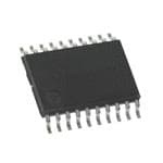
| 描述 | IC PROCESSOR FRONT END LP 20SSOP |
| 产品分类 | 数据采集 - 模拟前端 (AFE) |
| 品牌 | Analog Devices Inc |
| 数据手册 | |
| 产品图片 |
|
| 产品型号 | AD73311LARSZ-REEL7 |
| rohs | 无铅 / 符合限制有害物质指令(RoHS)规范要求 |
| 产品系列 | - |
| 位数 | 16 |
| 供应商器件封装 | 20-SSOP |
| 其它名称 | AD73311LARSZ-REEL7DKR |
| 功率(W) | 50mW |
| 包装 | Digi-Reel® |
| 封装/外壳 | 20-SSOP(0.209",5.30mm 宽) |
| 标准包装 | 1 |
| 电压-电源,数字 | 3V |
| 电压-电源,模拟 | 3V |
| 通道数 | 2 |


- 商务部:美国ITC正式对集成电路等产品启动337调查
- 曝三星4nm工艺存在良率问题 高通将骁龙8 Gen1或转产台积电
- 太阳诱电将投资9.5亿元在常州建新厂生产MLCC 预计2023年完工
- 英特尔发布欧洲新工厂建设计划 深化IDM 2.0 战略
- 台积电先进制程称霸业界 有大客户加持明年业绩稳了
- 达到5530亿美元!SIA预计今年全球半导体销售额将创下新高
- 英特尔拟将自动驾驶子公司Mobileye上市 估值或超500亿美元
- 三星加码芯片和SET,合并消费电子和移动部门,撤换高东真等 CEO
- 三星电子宣布重大人事变动 还合并消费电子和移动部门
- 海关总署:前11个月进口集成电路产品价值2.52万亿元 增长14.8%


PDF Datasheet 数据手册内容提取
a Low Cost, Low Power CMOS General Purpose Analog Front End AD73311L FEATURES GENERAL DESCRIPTION 16-Bit A/D Converter The AD73311L is a complete front-end processor for general 16-Bit D/A Converter purpose applications including speech and telephony. It features Programmable Input/Output Sample Rates a 16-bit A/D conversion channel and a 16-bit D/A conversion 76 dB ADC SNR channel. Each channel provides 70dB signal-to-noise ratio over 77 dB DAC SNR a voiceband signal bandwidth. The final channel bandwidth can Programmable Sampling Rate be reduced, and signal-to-noise ratio improved, by external 64 kS/s Maximum Sample Rate digital filtering in a DSP engine. –90 dB Crosstalk The AD73311L is suitable for a variety of applications in the Low Group Delay (25ms Typ per ADC Channel, speech and telephony area, including low bit rate, high quality 50 ms Typ per DAC Channel) compression, speech enhancement, recognition and synthesis. Programmable Input/Output Gain The low group delay characteristic of the part makes it suitable Flexible Serial Port Which Allows Up to Eight Devices for single or multichannel active control applications. to Be Connected in Cascade The gains of the A/D and D/A conversion channels are program- Single (+3 V) Supply Operation mable over 38 dB and 21 dB ranges respectively. An on-chip 33mW Max Power Consumption at 2.7V reference voltage is included to allow single supply operation. On-Chip Reference A serial port (SPORT) allows easy interfacing of single or cas- 20-Lead SOIC/SSOP/TSSOP Packages caded devices to industry standard DSP engines. APPLICATIONS The AD73311L is available in 20-lead SOIC, SSOP and General Purpose Analog I/O TSSOP packages. Speech Processing Cordless and Personal Communications Telephony Active Control of Sound and Vibration Data Communications FUNCTIONAL BLOCK DIAGRAM AVDD1 AVDD2 DVDD VINP ANALOG SDI SILNOGOLPEB-EANCDKE/D 0/P3G8dAB SMIGOAMDNAUA-LLDAOETGLOTRA DECIMATOR SDIFS VINN ENABLE SCLK SERIAL SDO I/O PORT SDOFS VOUTP +6P/–G15AdB LOCWO-PNATTIISMNSUE FOILUTSER LOWCSA-WPPAITASCCSHI TFEOIDLR-TER 1D-BAICT SMIGODMDIGAUI-LTDAAETLLOTRA INTERPOLATOR SE VOUTN MCLK RESET REFCAP REFERENCE AD73311L REFOUT AGND1 AGND2 DGND REV. A Information furnished by Analog Devices is believed to be accurate and reliable. However, no responsibility is assumed by Analog Devices for its use, nor for any infringements of patents or other rights of third parties One Technology Way, P.O. Box 9106, Norwood, MA 02062-9106, U.S.A. which may result from its use. No license is granted by implication or Tel: 781/329-4700 World Wide Web Site: http://www.analog.com otherwise under any patent or patent rights of Analog Devices. Fax: 781/326-8703 © Analog Devices, Inc., 2000
AD73311L–SPECIFICATIONS1 (AVDD = DVDD = 2.7V to 3.3 V; DGND = AGND = 0V, f = 16.384 MHz, DMCLK F = 8 kHz; T = T to T , unless otherwise noted.) S A MIN MAX AD73311LA Parameter Min Typ Max Unit Test Conditions/Comments REFERENCE REFCAP Absolute Voltage, V 1.08 1.2 1.32 V REFCAP REFCAP TC 50 ppm/°C 0.1µF Capacitor Required from REFOUT REFCAP to AGND2 Typical Output Impedance 145 Ω Absolute Voltage, V 1.08 1.2 1.32 V Unloaded REFOUT Minimum Load Resistance 1 kΩ Maximum Load Capacitance 100 pF ADC SPECIFICATIONS Maximum Input Range at VIN2, 3 1.578 V p-p Measured Differentially –2.85 dBm Max Input = (1.578/1.2) × V REFCAP Nominal Reference Level at VIN 1.0954 V p-p Measured Differentially (0 dBm0) –6.02 dBm Absolute Gain PGA = 0 dB –2.2 –0.6 +1.0 dB 1.0 kHz, 0 dBm0 PGA = 38 dB –1.0 dB 1.0 kHz, 0 dBm0 Gain Tracking Error ±0.1 dB 1.0 kHz, +3 dBm0 to –50 dBm0 Signal to (Noise + Distortion) Refer to Figure 5a PGA = 0 dB 71 76 dB 300 Hz to 3400 Hz 70 74 dB 0 Hz to f /2 SAMP 72 dB 300 Hz to 3400 Hz; f = 64 kHz SAMP 56 dB 0 Hz to f /2; f = 64 kHz SAMP SAMP PGA = 38 dB 60 dB 300 Hz to 3.4 kHz 59 dB 0 Hz to f /2 SAMP Total Harmonic Distortion PGA = 0 dB –85 –75 dB 300 Hz to 3.4 kHz PGA = 38 dB –85 dB 300 Hz to 3.4 kHz Intermodulation Distortion –82 dB PGA = 0 dB Idle Channel Noise –76 dBm0 PGA = 0 dB Crosstalk –100 dB ADC Input Signal Level: 1.0 kHz, 0dBm0 DAC Input at Idle DC Offset –20 +2 +25 mV PGA = 0 dB Power Supply Rejection –84 dB Input Signal Level at AVDD and DVDD Pins 1.0 kHz, 100 mV p-p Sine Wave Group Delay4, 5 25 µs 64 kHz Output Sample Rate Input Resistance at VIN2, 4 45 kΩ6 DMCLK = 16.384 MHz DAC SPECIFICATIONS Maximum Voltage Output Swing2 Single-Ended 1.578 V p-p PGA = 6 dB –2.85 dBm Max Output = (1.578/1.2) × V REFCAP Differential 3.156 V p-p PGA = 6 dB 3.17 dBm Max Output = 2 × ((1.578/1.2) × V REFCAP Nominal Voltage Output Swing (0 dBm0) Single-Ended 1.0954 V p-p PGA = 6 dB –6.02 dBm Differential 2.1909 V p-p PGA = 6 dB 0 dBm Output Bias Voltage4 1.08 1.2 1.32 V REFOUT Unloaded Absolute Gain –1.8 –0.7 +0.4 dB 1.0 kHz, 0 dBm0 Gain Tracking Error ±0.1 dB 1.0 kHz, +3 dBm0 to –50 dBm0 Signal to (Noise + Distortion) Refer to Figure 5b PGA = 0 dB 70 77 dB 300 Hz to 3.4 kHz Frequency Range 76 dB 300 Hz to 3400 Hz; f = 64 kHz SAMP PGA = 6 dB 77 dB 300 Hz to 3.4 kHz Frequency Range 77 dB 300 Hz to 3400 Hz; f = 64 kHz SAMP Total Harmonic Distortion PGA = 0 dB –80 –70 dB PGA = 6 dB –80 dB Intermodulation Distortion –76 dB PGA = 0 dB Idle Channel Noise –82 dBm0 PGA = 0 dB Crosstalk –100 dB ADC Input Signal Level: AGND; DAC Output Signal Level: 1.0 kHz, 0 dBm0 –2– REV. A
AD73311L AD73311LA Parameter Min Typ Max Unit Test Conditions/Comments DAC SPECIFICATIONS (Continued) Power Supply Rejection –81 dB Input Signal Level at AVDD and DVDD Pins: 1.0 kHz, 100 mV p-p Sine Wave Group Delay4, 5 25 µs 64 kHz Input Sample Rate, Interpolator Bypassed (CRE:5 = 1) Output DC Offset2, 7 –30 +5 +50 mV PGA = 6 dB Minimum Load Resistance, R 2, 8 L Single-Ended 150 Ω Differential 150 Ω Maximum Load Capacitance, C 2, 8 L Single-Ended 500 pF Differential 100 pF FREQUENCY RESPONSE (ADC AND DAC)9 Typical Output Normalized to f SAMP 0 0 dB 0.03125 –0.1 dB 0.0625 –0.25 dB 0.125 –0.6 dB 0.1875 –1.4 dB 0.25 –2.8 dB 0.3125 –4.5 dB Channel Frequency Response Is 0.375 –7.0 dB Programmable by Means of External 0.4375 –9.5 dB Digital Filtering > 0.5 < –12.5 dB LOGIC INPUTS V , Input High Voltage V – 0.8 V V INH DD DD V , Input Low Voltage 0 0.8 V INL I , Input Current 10 µA IH C , Input Capacitance 10 pF IN LOGIC OUTPUT V , Output High Voltage V – 0.4 V V |IOUT| ≤ 100 µA OH DD DD V , Output Low Voltage 0 0.4 V |IOUT| ≤ 100 µA OL Three-State Leakage Current –10 +10 µA POWER SUPPLIES AVDD1, AVDD2 2.7 3.3 V DVDD 2.7 3.3 V I 10 See Table I DD NOTES 1Operating temperature range is as follows: –40°C to +105°C. Therefore, T = –40°C and T = +105°C. MIN MAX 2Test conditions: Input PGA set for 0dB gain, Output PGA set for 6 dB gain, no load on analog outputs (unless otherwise noted). 3At input to sigma-delta modulator of ADC. 4Guaranteed by design. 5Overall group delay will be affected by the sample rate and the external digital filtering. 6The ADC’s input impedance is inversely proportional to DMCLK and is approximated by: (4 × 10¹¹)/DMCLK. 7Between VOUTP and VOUTN. 8At VOUT output. 9Frequency responses of ADC and DAC measured with input at audio reference level (the input level that produces an output level of –10 dBm0), with 38dB preamplifier bypassed and input gain of 0 dB. 10Test Conditions: no load on digital inputs, analog inputs ac coupled to ground, no load on analog outputs. Specifications subject to change without notice. Table I. Current Summary (AVDD = DVDD = 3.3V) Analog Internal Digital External Interface Total Current MCLK Conditions Current Current Current (Max) SE ON Comments ADC Only On 2 4.5 0.5 8.0 1 YES REFOUT Disabled ADC and DAC On 5.6 4.8 0.5 12.5 1 YES REFOUT Disabled REFCAP Only On 0.65 0 0 1.0 0 NO REFOUT Disabled REFCAP and REFOUT Only On 2.7 0 0 3.8 0 NO All Sections Off 0 0.6 0 0.75 0 YES MCLK Active Levels Equal to 0 V and DVDD All Sections Off 1 µA 0.5 µA 0 20 µA 0 NO Digital Inputs Static and Equal to 0 V or DVDD The above values are in mA and are typical values unless otherwise noted. REV. A –3–
AD73311L Table II. Signal Ranges Parameter Condition Signal Range V 1.2 V ± 10% REFCAP V 1.2 V ± 10% REFOUT ADC Maximum Input Range at V 1.578 V p-p IN Nominal Reference Level 1.0954 V p-p DAC Maximum Voltage Output Swing Single-Ended 1.578 V p-p Differential 3.156 V p-p Nominal Voltage Output Swing Single-Ended 1.0954 V p-p Differential 2.1909 V p-p Output Bias Voltage V REFOUT TIMING CHARACTERISTICS (AVDD = DVDD = 2.7 V to 3.6 V; AGND = DGND = 0 V; T = T to T , unless otherwise noted) A MlN MAX Limit at Parameter T = –40(cid:1)C to +105(cid:1)C Unit Description A Clock Signals See Figure 1 t 61 ns min MCLK Period 1 t 24.4 ns min MCLK Width High 2 t 24.4 ns min MCLK Width Low 3 Serial Port See Figures 3 and 4 t t ns min SCLK Period 4 1 t 0.4 × t ns min SCLK Width High 5 1 t 0.4 × t ns min SCLK Width Low 6 1 t 20 ns min SDI/SDIFS Setup Before SCLK Low 7 t 0 ns min SDI/SDIFS Hold After SCLK Low 8 t 10 ns max SDOFS Delay from SCLK High 9 t 10 ns min SDOFS Hold After SCLK High 10 t 10 ns min SDO Hold After SCLK High 11 t 10 ns max SDO Delay from SCLK High 12 t 30 ns max SCLK Delay from MCLK 13 t1 100(cid:2)A IOL t 2 TO OUTPUT 2.1V PIN CL 15pF t3 100(cid:2)A IOH Figure 1.MCLK Timing Figure 2.Load Circuit for Timing Specifications t 1 t t 2 3 MCLK t 13 SCLK* t5 t6 t 4 *SCLK IS INDIVIDUALLY PROGRAMMABLE IN FREQUENCY (MCLK/4 SHOWN HERE). Figure 3.SCLK Timing –4– REV. A
AD73311L SE (I) THREE- SCLK (O) STATE t 7 SDIFS (I) t 8 t 8 t 7 SDI (I) D15 D14 D1 D0 D15 THREE- t9 t10 SDOFS (O) STATE THREE- t12 t11 STATE SDO (O) D15 D2 D1 D0 D15 D14 Figure 4.Serial Port (SPORT) 80 80 70 70 60 60 50 50 B B D) – d40 D) – d40 N+30 N+30 S/( S/( 20 20 10 10 0 0 –10 –10 –85 –75 –65 –55 –45 –35 –25 –15 –5 0 –85 –75 –65 –55 –45 –35 –25 –15 –5 0 VIN – dBm0 3.17 VIN – dBm0 3.17 Figure 5a.S/(N+D) vs. V (ADC @ 3V) over Voiceband Figure 5b.S/(N+D) vs. V (DAC @ 3V) over Voiceband IN IN Bandwidth (300 Hz – 3.4kHz) Bandwidth (300 Hz – 3.4 kHz) REV. A –5–
AD73311L ABSOLUTE MAXIMUM RATINGS* PIN CONFIGURATION (T = 25°C unless otherwise noted) A AVDD, DVDD to GND . . . . . . . . . . . . . . . –0.3 V to +4.6 V AGND to DGND . . . . . . . . . . . . . . . . . . . . –0.3 V to +0.3 V VOUTP 1 20 SE Digital I/O Voltage to DGND . . . –0.3 V to (DVDD + 0.3 V) VOUTN 2 19 SDI Analog I/O Voltage to AGND . . . –0.3 V to (AVDD + 0.3 V) AVDD1 3 18 SDIFS Operating Temperature Range AGND1 4 17 SDOFS Industrial (A Version) . . . . . . . . . . . . . . . –40°C to +105°C VINP 5 AD73311L 16 SDO Storage Temperature Range . . . . . . . . . . . . –65°C to +150°C Maximum Junction Temperature . . . . . . . . . . . . . . . . 150°C VINN 6 (NToOt Pto V SIEcaWle) 15 MCLK SOIC, θ Thermal Impedance . . . . . . . . . . . . . . . . . 75°C/W REFOUT 7 14 SCLK JA Lead Temperature, Soldering REFCAP 8 13 RESET Vapor Phase (60 sec) . . . . . . . . . . . . . . . . . . . . . . . . 215°C AVDD2 9 12 DVDD Infrared (15 sec) . . . . . . . . . . . . . . . . . . . . . . . . . . . . 220°C AGND2 10 11 DGND SSOP, θ Thermal Impedance . . . . . . . . . . . . . . . . 126°C/W JA Lead Temperature, Soldering Vapor Phase (60 sec) . . . . . . . . . . . . . . . . . . . . . . . . 215°C Infrared (15 sec) . . . . . . . . . . . . . . . . . . . . . . . . . . . . 220°C TSSOP, θ Thermal Impedance . . . . . . . . . . . . . . . 143°C/W ORDERING GUIDE JA Lead Temperature, Soldering Vapor Phase (60 sec) . . . . . . . . . . . . . . . . . . . . . . . . 215°C Temperature Package Infrared (15 sec) . . . . . . . . . . . . . . . . . . . . . . . . . . . . 220°C Model Range Option1 AD73311LAR –40°C to +105°C R-20 *Stresses above those listed under Absolute Maximum Ratings may cause perma- nent damage to the device. This is a stress rating only; functional operation of the AD73311LARS –40°C to +105°C RS-20 device at these or any other conditions above those listed in the operational sections AD73311LARU –40°C to +105°C RU-20 of this specification is not implied. Exposure to absolute maximum rating condi- EVAL-AD73311LEB Evaluation Board2 tions for extended periods may affect device reliability. NOTES 1R = 0.3' Small Outline IC (SOIC), RS = Shrink Small Outline Package (SSOP), RU = Thin Small Shrink Outline Package (TSSOP). 2The AD73311L evaluation board features a cascade of two codecs interfaced to an ADSP-2185L DSP. The board features a DSP software monitor which allows interface to a PC serial port. CAUTION ESD (electrostatic discharge) sensitive device. Electrostatic charges as high as 4000V readily WARNING! accumulate on the human body and test equipment and can discharge without detection. Although the AD73311L features proprietary ESD protection circuitry, permanent damage may occur on devices subjected to high energy electrostatic discharges. Therefore, proper ESD ESD SENSITIVE DEVICE precautions are recommended to avoid performance degradation or loss of functionality. –6– REV. A
AD73311L PIN FUNCTION DESCRIPTIONS Pin Number Mnemonic Function 1 VOUTP Analog Output from the Positive Terminal of the Output Channel. 2 VOUTN Analog Output from the Negative Terminal of the Output Channel. 3 AVDD1 Analog Power Supply Connection for the Output Driver. 4 AGND1 Analog Ground Connection for the Output Driver. 5 VINP Analog Input to the Positive Terminal of the Input Channel. 6 VINN Analog Input to the Negative Terminal of the Input Channel. 7 REFOUT Buffered Reference Output, which has a nominal value of 1.2V. 8 REFCAP A Bypass Capacitor to AGND2 of 0.1µF is required for the on-chip reference. The capacitor should be fixed to this pin. 9 AVDD2 Analog Power Supply Connection. 10 AGND2 Analog Ground/Substrate Connection. 11 DGND Digital Ground/Substrate Connection. 12 DVDD Digital Power Supply Connection. 13 RESET Active Low Reset Signal. This input resets the entire chip, resetting the control registers and clearing the digital circuitry. 14 SCLK Output Serial Clock whose rate determines the serial transfer rate to/from the codec. It is used to clock data or control information to and from the serial port (SPORT). The frequency of SCLK is equal to the frequency of the master clock (MCLK) divided by an integer number—this integer number being the product of the external master clock rate divider and the serial clock rate divider. 15 MCLK Master Clock Input. MCLK is driven from an external clock signal. 16 SDO Serial Data Output of the Codec. Both data and control information may be output on this pin and are clocked on the positive edge of SCLK. SDO is in three-state when no information is being transmitted and when SE is low. 17 SDOFS Framing Signal Output for SDO Serial Transfers. The frame sync is on bit wide and is active one SCLK period before the first bit (MSB) of each output word. SDOFS is referenced to the positive edge of SCLK. SDOFS is in three-state when SE is low. 18 SDIFS Framing Signal Input for SDI Serial Transfers. The frame sync is one bit wide and is valid one SCLK period before the first bit (MSB) of each input word. SDIFS is sampled on the negative edge of SCLK and ignored when SE is low. 19 SDI Serial Data Input of the Codec. Both data and control information may be input on this pin and are clocked on the negative edge of SCLK. SDI is ignored when SE is low. 20 SE SPORT Enable. Asynchronous input enable pin for the SPORT. When SE is set low by the DSP, the output pins of the SPORT are three-stated and the input pins are ignored. SCLK is also disabled internally in order to decrease power dissipation. When SE is brought high, the control and data regis- ters of the SPORT are at their original values (before SE was brought low); however, the timing counters and other internal registers are at their reset values. REV. A –7–
AD73311L TERMINOLOGY ABBREVIATIONS Absolute Gain ADC Analog-to-Digital Converter. Absolute gain is a measure of converter gain for a known signal. ALB Analog Loop-Back. Absolute gain is measured (differentially) with a 1 kHz sine wave at 0 dBm0 for the DAC and with a 1 kHz sine wave at 0dBm0 BW Bandwidth. for the ADC. The absolute gain specification is used for gain CRx A Control Register where x is a placeholder for an tracking error specification. alphabetic character (A–E). There are five read/ Crosstalk write control registers on the AD73311L—desig- Crosstalk is due to coupling of signals from a given channel nated CRA through CRE. to an adjacent channel. It is defined as the ratio of the ampli- CRx:n A bit position, where n is a placeholder for a tude of the coupled signal to the amplitude of the input signal. numeric character (0–7), within a control register; Crosstalk is expressed in dB. where x is a placeholder for an alphabetic charac- Gain Tracking Error ter (A–E). Position 7 represents the MSB and Gain tracking error measures changes in converter output for Position 0 represents the LSB. different signal levels relative to an absolute signal level. The DAC Digital-to-Analog Converter. absolute signal level is 0 dBm0 (equal to absolute gain) at 1 kHz DLB Digital Loop-Back. for the DAC and 0 dBm0 (equal to absolute gain) at 1 kHz for the ADC. Gain tracking error at 0 dBm0 (ADC) and 0 dBm0 DMCLK Device (Internal) Master Clock. This is the (DAC) is 0 dB by definition. internal master clock resulting from the external master clock (MCLK) being divided by the on-chip Group Delay master clock divider. Group delay is defined as the derivative of radian phase with respect to radian frequency, dø(f)/df. Group delay is a measure FSLB Frame Sync Loop-Back—where the SDOFS of of average delay of a system as a function of frequency. A linear the final device in a cascade is connected to the system with a constant group delay has a linear phase response. RFS and TFS of the DSP and the SDIFS of first The deviation of group delay from a constant indicates the degree device in the cascade. Data input and output of nonlinear phase response of the system. occur simultaneously. In the case of nonFSLB, SDOFS and SDO are connected to the Rx Port Idle Channel Noise of the DSP while SDIFS and SDI are connected Idle channel noise is defined as the total signal energy measured to the Tx Port. at the output of the device when the input is grounded (measured in the frequency range 300Hz–3400 Hz). PGA Programmable Gain Amplifier. Intermodulation Distortion SC Switched Capacitor. With inputs consisting of sine waves at two frequencies, fa and SNR Signal-to-Noise Ratio. fb, any active device with nonlinearities will create distortion products at sum and difference frequencies of mfa ± nfb where SPORT Serial Port. m, n = 0, 1, 2, 3, etc. Intermodulation terms are those for which THD Total Harmonic Distortion. neither m nor n are equal to zero. For final testing, the second VBW Voice Bandwidth. order terms include (fa + fb) and (fa – fb), while the third order terms include (2fa + fb), (2fa – fb), (fa + 2fb) and (fa – 2fb). Power Supply Rejection Power supply rejection measures the susceptibility of a device to noise on the power supply. Power supply rejection is measured by modulating the power supply with a sine wave and measuring the noise at the output (relative to 0 dB). Sample Rate The sample rate is the rate at which the ADC updates its out- put register and the DAC updates its output from its input register. It is fixed relative to the DMCLK (= DMCLK/256) and therefore may only be changed by changing the DMCLK. SNR+THD Signal-to-noise ratio plus harmonic distortion is defined to be the ratio of the rms value of the measured input signal to the rms sum of all other spectral components in the frequency range 300Hz–3400 Hz, including harmonics but excluding dc. –8– REV. A
AD73311L FUNCTIONAL DESCRIPTION sampling rate of the sigma-delta modulator is DMCLK/8. The Encoder Channel main effect of oversampling is that the quantization noise is The encoder channel consists of an input configuration block, a spread over a very wide bandwidth, up to F /2 = DMCLK/16 S switched capacitor PGA and a sigma-delta analog-to-digital (Figure 6a). This means that the noise in the band of interest is converter (ADC). An on-board digital filter, which forms part much reduced. Another complementary feature of sigma-delta of the sigma-delta ADC, also performs critical system-level converters is the use of a technique called noise-shaping. This filtering. Due to the high level of oversampling, the input anti- technique has the effect of pushing the noise from the band of alias requirements are reduced such that a simple single pole interest to an out-of-band position (Figure 6b). The combi- RC stage is sufficient to give adequate attenuation in the band nation of these techniques, followed by the application of a of interest. digital filter, reduces the noise in band sufficiently to ensure good dynamic performance from the part (Figure 6c). Input Configuration Block The input configuration block consists of a multiplexing arrange- ment that allows selection of various input configurations. This includes ADC input selection from either the VINP, VINN pins or from the DAC output via the Analog Loop-Back (ALB) arrangement. Differential inputs can be inverted and it is also possible to use the device in single-ended mode, which allows the option of using the VINP, VINN pins as two separate B AONFD FS/2 single-ended inputs, either of which can be selected under INTEREST DMCLK/16 software control. a. Programmable Gain Amplifier The encoder section’s analog front end comprises a switched capacitor PGA that also forms part of the sigma-delta modulator. The SC sampling frequency is DMCLK/8. The PGA, whose programmable gain settings are shown in Table III, may be NOISE-SHAPING used to increase the signal level applied to the ADC from low output sources such as microphones, and can be used to avoid B AONFD FS/2 placing external amplifiers in the circuit. The input signal level INTEREST DMCLK/16 to the sigma-delta modulator should not exceed the maximum b. input voltage permitted. The PGA gain is set by bits IGS0, IGS1 and IGS2 (CRD:0–2) in Control Register D. DIGITAL FILTER Table III. PGA Settings for the Encoder Channel IGS2 IGS1 IGS0 Gain (dB) 0 0 0 0 INTBE AORNFEDST DMFCSL/K2/16 0 0 1 6 c. 0 1 0 12 Figure 6.Sigma-Delta Noise Reduction 0 1 1 18 1 0 0 20 Figure 7 shows the various stages of filtering that are employed 1 0 1 26 in a typical AD73311L application. In Figure 7a we see the 1 1 0 32 transfer function of the external analog antialias filter. Even 1 1 1 38 though it is a single RC pole, its cutoff frequency is sufficiently far away from the initial sampling frequency (DMCLK/8) that it takes care of any signals that could be aliased by the sampling ADC frequency. This also shows the major difference between the The ADC consists of an analog sigma-delta modulator and a initial oversampling rate and the bandwidth of interest. In Figure digital antialiasing decimation filter. The sigma-delta modu- 7b, the signal and noise-shaping responses of the sigma-delta lator noise-shapes the signal and produces 1-bit samples at a modulator are shown. The signal response provides further DMCLK/8 rate. This bitstream, representing the analog input rejection of any high frequency signals while the noise-shaping signal, is input to the antialiasing decimation filter. The decima- will push the inherent quantization noise to an out-of-band tion filter reduces the sample rate and increases the resolution. position. The detail of Figure 7c shows the response of the Analog Sigma-Delta Modulator digital decimation filter (Sinc-cubed response) with nulls every The AD73311L input channel employs a sigma-delta conver- multiple of DMCLK/256, which is the decimation filter update sion technique, which provides a high resolution 16-bit output rate. The final detail in Figure 7d shows the application of a with system filtering being implemented on-chip. final antialias filter in the DSP engine. This has the advantage of being implemented according to the user’s requirements and Sigma-delta converters employ a technique known as over- available MIPS. The filtering in Figures 7a through 7c is imple- sampling, where the sampling rate is many times the highest mented in the AD73311L. frequency of interest. In the case of the AD73311L, the initial REV. A –9–
AD73311L ADC Coding The ADC coding scheme is in twos complement format (see Figure 8). The output words are formed by the decimation filter, which grows the word length from the single-bit output of the sigma-delta modulator to a 15-bit word, which is the 16-bit transfer being used as a flag bit to indicate either control or data in the frame. FB = 4kHz FSINIT = DMCLK/8 a.Analog Antialias Filter Transfer Function VREF + (VREF (cid:3) 0.32875) VINN SIGNAL TRANSFER FUNCTION AINNAPLUOTG VREF NOISE TRANSFER FUNCTION VREF – (VREF (cid:3) 0.32875) VINP 10...00 00...00 01...11 FB = 4kHz FSINIT = DMCLK/8 ADC CODE DIFFERENTIAL b.Analog Sigma-Delta Modulator Transfer Function VREF + (VREF (cid:3) 0.6575) VINN AINNAPLUOTG VREF VREF – (VREF (cid:3) 0.6575) VINP FB = 4kHz FSINTER = DMCLK/256 10...00 00...00 01...11 c.Digital Decimator Transfer Function ADC CODE SINGLE-ENDED Figure 8.ADC Transfer Function Decoder Channel The decoder channel consists of a digital interpolator, digital sigma-delta modulator, a single bit digital-to-analog converter (DAC), an analog smoothing filter and a programmable gain amplifier with differential output. DAC Coding FB = 4kHz FSFINAL = 8kHz FSINTER = DMCLK/256 The DAC coding scheme is in twos complement format with d.Final Filter LPF (HPF) Transfer Function 0x7FFF being full-scale positive and 0x8000 being full-scale Figure 7.AD73311L ADC Frequency Responses negative. Decimation Filter Interpolation Filter The digital filter used in the AD73311L carries out two impor- The anti-imaging interpolation filter is a sinc-cubed digital filter tant functions. Firstly, it removes the out-of-band quantization which up-samples the 16-bit input words from the SPORT noise, which is shaped by the analog modulator and secondly, it input rate of DMCLK/M (where M depends on the sample rate decimates the high frequency bitstream to a lower rate 15-bit word. setting—M = 256 @ 64 kHz; M = 512 @ 32 kHz, M = 1024 @ The antialiasing decimation filter is a sinc-cubed digital filter 16 kHz, M = 2048 @ 8 kHz), to a rate of DMCLK/8 while that reduces the sampling rate from DMCLK/8 at the modula- filtering to attenuate images produced by the interpolation pro- tor to an output rate at the SPORT of DMCLK/M (where M cess. Its Z transform is given as: [(1–Z–N)/(1–Z–1)]3 where N is depends on the sample rate setting—M = 256 @ 64 kHz; M = determined by the sampling rate (N = 32 @ 64 kHz, N = 64 @ 512 @ 32 kHz, M = 1024 @ 16 kHz, M = 2048 @ 8 kHz), and 32 kHz, N = 128 @ 16 kHz, N = 256 @ 8 kHz). The DAC increases the resolution from a single bit to 15 bits. Its Z trans- receives 16-bit samples from the host DSP processor at a rate of form is given as: [(1–Z–N)/(1–Z–1)]3 where N is determined by DMCLK/M. If the host processor fails to write a new value to the sampling rate (N = 32 @ 64 kHz, N = 64 @ 32 kHz, N = the serial port, the existing (previous) data is read again. The 128 @ 16 kHz, N = 256 @ 8 kHz). This ensures a minimal data stream is filtered by the anti-imaging interpolation filter, group delay of 25 µs at the 64 kHz sampling rate. but there is an option to bypass the interpolator for the mini- mum group delay configuration by setting the IBYP bit (CRE:5) of Control Register E. The interpolation filter has the same charac- teristics as the ADC’s antialiasing decimation filter. –10– REV. A
AD73311L The output of the interpolation filter is fed to the DAC’s digital SPORT Overview sigma-delta modulator, which converts the 16-bit data to 1-bit The AD73311L SPORT is a flexible, full-duplex, synchronous samples at a rate of DMCLK/8. The modulator noise-shapes serial port whose protocol has been designed to allow up to eight the signal so that errors inherent to the process are minimized AD73311L devices to be connected, in cascade, to a single DSP in the passband of the converter. The bitstream output of the via a six-wire interface. It has a very flexible architecture that can sigma-delta modulator is fed to the single bit DAC where it is be configured by programming two of the internal control regis- converted to an analog voltage. ters. The AD73311L SPORT has three distinct modes of opera- tion: Control Mode, Data Mode and Mixed Control/Data Mode. Analog Smoothing Filter and PGA The output of the single-bit DAC is sampled at DMCLK/8, In Control Mode (CRA:0 = 0), the device’s internal configura- therefore it is necessary to filter the output to reconstruct the tion can be programmed by writing to the five internal control low frequency signal. The decoder’s analog smoothing filter registers. In this mode, control information can be written to or consists of a continuous-time filter preceded by a third-order read from the codec. In Data Mode (CRA:0 = 1), information switched-capacitor filter. The continuous-time filter forms part that is sent to the device is used to update the decoder section of the output programmable gain amplifier (PGA). The PGA (DAC), while the encoder section (ADC) data is read from the can be used to adjust the output signal level from –15 dB to device. In this mode, only DAC and ADC data is written to or +6dB in 3 dB steps, as shown in Table IV. The PGA gain is read from the device. Mixed mode (CRA:0 = 1 and CRA:1 = 1) set by bits OGS0, OGS1 and OGS2 (CRD:4-6) in Control allows the user to choose whether the information being sent to Register D. the device contains either control information or DAC data. This is achieved by using the MSB of the 16-bit frame as a flag Table IV. PGA Settings for the Decoder Channel bit. Mixed mode reduces the resolution to 15 bits with the MSB being used to indicate whether the information in the 16-bit OGS2 OGS1 OGS0 Gain (dB) frame is control information or DAC/ADC data. 0 0 0 +6 The SPORT features a single 16-bit serial register that is used 0 0 1 +3 for both input and output data transfers. As the input and out- 0 1 0 0 put data must share the same register there are some precautions 0 1 1 –3 that must be observed. The primary precaution is that no infor- 1 0 0 –6 mation must be written to the SPORT without reference to an 1 0 1 –9 output sample event, which is when the serial register will be 1 1 0 –12 overwritten with the latest ADC sample word. Once the SPORT 1 1 1 –15 starts to output the latest ADC word then it is safe for the DSP to write new control or data words to the codec. In certain con- Differential Output Amplifiers figurations, data can be written to the device to coincide with The decoder has a differential analog output pair (VOUTP and the output sample being shifted out of the serial register—see VOUTN). The output channel can be muted by setting the section on interfacing devices. The serial clock rate (CRB:2–3) MUTE bit (CRD:7) in Control Register D. The output signal defines how many 16-bit words can be written to a device before is dc-biased to the codec’s on-chip voltage reference. the next output sample event will happen. Voltage Reference The SPORT block diagram, shown in Figure 9, details the six The AD73311L reference, REFCAP, is a bandgap reference control registers (A–F), external MCLK to internal DMCLK that provides a low noise, temperature-compensated reference divider and serial clock divider. The divider rates are controlled to the DAC and ADC. A buffered version of the reference is by the setting of Control Register B. The AD73311L features a also made available on the REFOUT pin and can be used to master clock divider that allows users the flexibility of dividing bias other external analog circuitry. The reference has a default externally available high frequency DSP or CPU clocks to gener- nominal value of 1.2V. ate a lower frequency master clock internally in the codec which The reference output (REFOUT) can be enabled for biasing may be more suitable for either serial transfer or sampling rate external circuitry by setting the RU bit (CRC:6) of CRC. requirements. The master clock divider has five divider options (÷1 default condition, ÷2, ÷3, ÷4, ÷5) that are set by loading Serial Port (SPORT) the master clock divider field in Register B with the appropriate The codec communicates with a host processor via the bidirec- code. Once the internal device master clock (DMCLK) has tional synchronous serial port (SPORT) which is compatible been set using the master clock divider, the sample rate and with most modern DSPs. The SPORT is used to transmit and serial clock settings are derived from DMCLK. receive digital data and control information. The SPORT can work at four different serial clock (SCLK) rates: In both transmit and receive modes, data is transferred at the chosen from DMCLK, DMCLK/2, DMCLK/4 or DMCLK/8, serial clock (SCLK) rate with the MSB being transferred first. where DMCLK is the internal or device master clock resulting Due to the fact that the SPORT uses a common serial register for from the external or pin master clock being divided by the serial input and output, communications between an AD73311L master clock divider. When working at the lower SCLK rate of codec and a host processor (DSP engine) must always be initi- DMCLK/8, which is intended for interfacing with slower DSPs, ated by the codec itself. This ensures that there is no danger of the SPORT will support a maximum of two devices in cascade the information being sent to the codec being corrupted by with the sample rate of DMCLK/256. ADC samples being output by the codec. REV. A –11–
AD73311L MCLK DMCLK (EXTERNAL) (INTERNAL) MCLK DIVIDER 3 SE SE(RSIPAOL RPTO)RT DSIVCIDLEKR SCLK RESET SDIFS SDOFS SDI SSEERRIIAALL RREEGGISISTTEERR SDO 2 8 8 8 8 8 8 CONTROL CONTROL CONTROL CONTROL CONTROL CONTROL REGISTER A REGISTER B REGISTER C REGISTER D REGISTER E REGISTER F Figure 9.SPORT Block Diagram SPORT Register Maps is programmable by setting bits CRB:2–3. Table VI shows the There are two register banks for the AD73311L: the control serial clock rate corresponding to the various bit settings. register bank and the data register bank. The control register Table VI. SCLK Rate Divider Settings bank consists of six read/write registers, each eight bits wide. Table IX shows the control register map for the AD73311L. SCD1 SCD0 SCLK Rate The first two control registers, CRA and CRB, are reserved for 0 0 DMCLK/8 controlling the SPORT. They hold settings for parameters such 0 1 DMCLK/4 as bit rate, internal master clock rate and device count (used 1 0 DMCLK/2 when more than one AD73311L is connected in cascade from 1 1 DMCLK a single SPORT). The other three registers; CRC, CRD and CRE are used to hold control settings for the ADC, DAC, Reference and Power Control sections of the device. Control Sample Rate Divider registers are written to on the negative edge of SCLK. The The AD73311L features a programmable sample rate divider data register bank consists of two 16-bit registers that are the that allows users flexibility in matching the codec’s ADC and DAC and ADC registers. DAC sample rates to the needs of the DSP software. The maxi- mum sample rate available is DMCLK/256 which offers the Master Clock Divider lowest conversion group delay, while the other available rates The AD73311L features a programmable master clock divider are: DMCLK/512, DMCLK/1024 and DMCLK/2048. The that allows the user to reduce an externally available master slowest rate (DMCLK/2048) is the default sample rate. The clock, at pin MCLK, by one of the ratios 1, 2, 3, 4 or 5 to sample rate divider is programmable by setting bits CRB:0-1. produce an internal master clock signal (DMCLK) that is used Table VII shows the sample rate corresponding to the various to calculate the sampling and serial clock rates. The master bit settings. clock divider is programmable by setting CRB:4-6. Table V shows the division ratio corresponding to the various bit settings. The Table VII. Sample Rate Divider Settings default divider ratio is divide-by-one. DIR1 DIR0 SCLK Rate Table V. DMCLK (Internal) Rate Divider Settings 0 0 DMCLK/2048 MCD2 MCD1 MCD0 DMCLK Rate 0 1 DMCLK/1024 1 0 DMCLK/512 0 0 0 MCLK 1 1 DMCLK/256 0 0 1 MCLK/2 0 1 0 MCLK/3 DAC Advance Register 0 1 1 MCLK/4 The loading of the DAC is internally synchronized with the 1 0 0 MCLK/5 unloading of the ADC data in each sampling interval. The 1 0 1 MCLK default DAC load event happens one SCLK cycle before the 1 1 0 MCLK SDOFS flag is raised by the ADC data being ready. However, 1 1 1 MCLK this DAC load position can be advanced before this time by modifying the contents of the DAC Advance field in Control Serial Clock Rate Divider Register E (CRE:0–4). The field is five bits wide, allowing 31 The AD73311L features a programmable serial clock divider that increments of weight 1/(DMCLK/8); see Table VIII. In certain allows users to match the serial clock (SCLK) rate of the data to circumstances this can reduce the group delay when the ADC that of the DSP engine or host processor. The maximum SCLK and DAC are used to process data in series. Appendix E details rate available is DMCLK and the other available rates are: how the DAC advance feature can be used. DMCLK/2, DMCLK/4 and DMCLK/8. The slowest rate (DMCLK/8) is the default SCLK rate. The serial clock divider NOTE: The DAC advance register should be changed before the DAC section is powered up. –12– REV. A
AD73311L Table VIII. DAC Timing Control that the device must be programmed to the correct settings after power-up or reset. Following a reset, the SDOFS will be asserted DA4 DA3 DA2 DA1 DA0 Time Advance* 2048 DMCLK cycles after RESET going high. The data that 0 0 0 0 0 0 ns is output following RESET and during Program Mode is ran- 0 0 0 0 1 488.2 ns dom and contains no valid information until either Data or 0 0 0 1 0 976.5 ns Mixed Mode is set. — — — — — — Power Management 1 1 1 1 0 14.64 µs The individual functional blocks of the AD73311L can be 1 1 1 1 1 15.13 µs enabled separately by programming the power control register CRC. It allows certain sections to be powered down if not *DMCLK = 16.384 MHz. required, which adds to the device’s flexibility in that the user OPERATION need not incur the penalty of having to provide power for a Resetting the AD73311L certain section if it is not necessary to their design. The power The pin RESET resets all the control registers. All registers are control register provides individual control settings for the major reset to zero indicating that the default SCLK rate (DMCLK/8) functional blocks and also a global override that allows all sec- and sample rate (DMCLK/2048) are at a minimum to ensure tions to be powered up by setting the bit. Using this method the that slow speed DSP engines can communicate effectively. As user could, for example, individually enable a certain section, well as resetting the control registers using the RESET pin, the such as the reference (CRC:5), and disable all others. The glo- device can be reset using the RESET bit (CRA:7) in Control bal power-up (CRC:0) can be used to enable all sections but if Register A. Both hardware and software resets require 4 DMCLK power-down is required using the global control, the reference cycles. On reset, DATA/PGM (CRA:0) is set to 0 (default condi- will still be enabled, in this case, because its individual bit is set. tion) thus enabling Program Mode. The reset conditions ensure Refer to Table XIII for details of the settings of CRC. Table IX. Control Register Map Address (Binary) Name Description Type Width Reset Setting (Hex) 000 CRA Control Register A R/W 8 0x00 001 CRB Control Register B R/W 8 0x00 010 CRC Control Register C R/W 8 0x00 011 CRD Control Register D R/W 8 0x00 100 CRE Control Register E R/W 8 0x00 101 CRF Control Register F R/W 8 0x00 110 to 111 Reserved Table X. Control Word Description 15 14 13 12 11 10 9 8 7 6 5 4 3 2 1 0 C/D R/W Device Address Register Address Register Data Control Frame Description Bit 15 Control/Data When set high, it signifies a control word in Program or Mixed Program/Data Modes. When set low, it signifies a data word in Mixed Program/Data Mode or an invalid control word in Program Mode. Bit 14 Read/Write When set low, it tells the device that the data field is to be written to the register selected by the register field setting provided the address field is zero. When set high, it tells the device that the selected register is to be written to the data field in the input serial register and that the new control word is to be output from the device via the serial output. Bits 13–11 Device Address This 3-bit field holds the address information. Only when this field is zero is a device selected. If the address is not zero, it is decremented and the control word is passed out of the device via the serial output. Bits 10–8 Register Address This 3-bit field is used to select one of the five control registers on the AD73311L. Bits 7–0 Register Data This 8-bit field holds the data that is to be written to or read from the selected register provided the address field is zero. REV. A –13–
AD73311L Table XI. Control Register A Description CONTROL REGISTER A 7 6 5 4 3 2 1 0 RESET DC2 DC1 DC0 SLB DLB MM DATA/PGM Bit Name Description 0 DATA/PGM Operating Mode (0 = Program; 1 = Data Mode) 1 MM Mixed Mode (0 = Off; 1 = Enabled) 2 DLB Digital Loop-Back Mode (0 = Off; 1 = Enabled) 3 SLB SPORT Loop-Back Mode (0 = Off; 1 = Enabled) 4 DC0 Device Count (Bit 0) 5 DC1 Device Count (Bit 1) 6 DC2 Device Count (Bit 2) 7 RESET Software Reset (0 = Off; 1 = Initiates Reset) Table XII. Control Register B Description CONTROL REGISTER B 7 6 5 4 3 2 1 0 CEE MCD2 MCD1 MCD0 SCD1 SCD0 DIR1 DIR0 Bit Name Description 0 DIR0 Decimation/Interpolation Rate (Bit 0) 1 DIR1 Decimation/Interpolation Rate (Bit 1) 2 SCD0 Serial Clock Divider (Bit 0) 3 SCD1 Serial Clock Divider (Bit 1) 4 MCD0 Master Clock Divider (Bit 0) 5 MCD1 Master Clock Divider (Bit 1) 6 MCD2 Master Clock Divider (Bit 2) 7 CEE Control Echo Enable (0 = Off; 1 = Enabled) Table XIII. Control Register C Description CONTROL REGISTER C 7 6 5 4 3 2 1 0 – RU PUREF PUDAC PUADC – – PU Bit Name Description 0 PU Power-Up Device (0 = Power Down; 1 = Power On) 1 Reserved Must Be Programmed to Zero (0) 2 Reserved Must Be Programmed to Zero (0) 3 PUADC ADC Power (0 = Power Down; 1 = Power On) 4 PUDAC DAC Power (0 = Power Down; 1 = Power On) 5 PUREF REF Power (0 = Power Down; 1 = Power On) 6 RU REFOUT Use (0 = Disable REFOUT; 1 = Enable REFOUT) 7 Reserved Must Be Programmed to Zero (0) –14– REV. A
AD73311L Table XIV. Control Register D Description CONTROL REGISTER D 7 6 5 4 3 2 1 0 MUTE OGS2 OGS1 OGS0 RMOD IGS2 IGS1 IGS0 Bit Name Description 0 IGS0 Input Gain Select (Bit 0) 1 IGS1 Input Gain Select (Bit 1) 2 IGS2 Input Gain Select (Bit 2) 3 RMOD Reset ADC Modulator (0 = Off; 1 = Reset Enabled) 4 OGS0 Output Gain Select (Bit 0) 5 OGS1 Output Gain Select (Bit 1) 6 OGS2 Output Gain Select (Bit 2) 7 MUTE Output Mute (0 = Mute Off; 1 = Mute Enabled) Table XV. Control Register E Description CONTROL REGISTER E 7 6 5 4 3 2 1 0 – – IBYP DA4 DA3 DA2 DA1 DA0 Bit Name Description 0 DA0 DAC Advance Setting (Bit 0) 1 DA1 DAC Advance Setting (Bit 1) 2 DA2 DAC Advance Setting (Bit 2) 3 DA3 DAC Advance Setting (Bit 3) 4 DA4 DAC Advance Setting (Bit 4) 5 IBYP Interpolator Bypass (0 = Bypass Disabled; 1 = Bypass Enabled) 6 Reserved Must Be Programmed to Zero (0) 7 Reserved Must Be Programmed to Zero (0) Table XVI. Control Register F Description CONTROL REGISTER F 7 6 5 4 3 2 1 0 ALB INV SEEN – – – – – Bit Name Description 0 Reserved Must Be Programmed to Zero (0) 1 Reserved Must Be Programmed to Zero (0) 2 Reserved Must Be Programmed to Zero (0) 3 Reserved Must Be Programmed to Zero (0) 4 Reserved Must Be Programmed to Zero (0) 5 SEEN Single-Ended Enable (0 = Disabled; 1 = Enabled) 6 INV Input Invert (0 = Disabled; 1 = Enabled) 7 ALB Analog Loopback of Output to Input (0 = Disabled; 1 = Enabled) REV. A –15–
AD73311L Operating Modes received at the SDIFS pin. When that number equals the device There are five operating modes available on the AD73311L. count stored in the device count field of CRA, the device knows Two of these—Digital Loop-Back and Sport Loop-Back—are that the present data frame being received is its own DAC update provided as diagnostic modes with the other three, Program, data. When the device is in normal Data Mode (i.e., mixed Data and Mixed Program/Data, being available for general mode disabled), it must receive a hardware reset to reprogram purpose use. The device configuration—register settings—can any of the control register settings. In a single codec configura- be changed only in Program and Mixed Program/Data Modes. tion, each 16-bit data frame sent from the DSP to the device is In all modes, transfers of information to or from the device interpreted as DAC data. The default device count is 1, therefore occur in 16-bit packets, therefore the DSP engine’s SPORT will each input frame sync will cause the 16-bit data frame to be be programmed for 16-bit transfers. loaded to the DAC register. Program (Control) Mode Mixed Program/Data Mode In Program Mode, CRA:0 = 0, the user writes to the control This mode allows the user to send control words to the device registers to set up the device for desired operation—SPORT along with the DAC data. This permits adaptive control of the operation, cascade length, power management, input/output device whereby control of the input/output gains can be effected gain, etc. In this mode, the 16-bit information packet sent to the by interleaving control words along with the normal flow of device by the DSP engine is interpreted as a control word whose DAC data. The standard data frame remains 16 bits, but now format is shown in Table X. In this mode, the user must address the MSB is used as a flag bit to indicate whether the remaining the device to be programmed using the address field of the control 15 bits of the frame represent DAC data or control information. word. This field is read by the device and if it is zero (000 bin) In the case of DAC data, the 15 bits are loaded with MSB justi- then the device recognizes the word as being addressed to it. If the fication and LSB set to 0 to the DAC register. Mixed mode is address field is not zero, it is then decremented and the control enabled by setting the MM bit (CRA:1) to 1 and the DATA/PGM word is passed out of the device—either to the next device in a bit (CRA:0) to 1. In the case where control setting changes will cascade or back to the DSP engine. This 3-bit address format be required during normal operation, this mode allows the allows the user to uniquely address any one of up to eight devices ability to load both control and data information with the slight in a cascade; please note that this addressing scheme is valid only inconvenience of formatting the data. Note that the output in sending control information to the device —a different format samples from the ADC will also have the MSB set to zero to is used to send DAC data to the device(s). In a single codec indicate it is a data word. configuration, all control word addresses must be zero, other- Digital Loop-Back wise they will not be recognized; in a multi-codec configuration This mode can be used for diagnostic purposes and allows the all addresses from zero to N-1 (where N = number of devices in user to feed the ADC samples from the ADC register directly to cascade) are valid. the DAC register. This forms a loop-back of the analog input to Following reset, when the SE pin is enabled, the codec responds the analog output by reconstructing the encoded signal using by raising the SDOFS pin to indicate that an output sample the decoder channel. The serial interface will continue to work, event has occurred. Control words can be written to the device to which allows the user to control gain settings, etc. Only when coincide with the data being sent out of the SPORT, as shown in DLB is enabled with Mixed Mode operation can the user disable Figure 10, or they can lag the output words by a time interval the DLB, otherwise the device must be reset. that should not exceed the sample interval. After reset, output Sport Loop-Back frame sync pulses will occur at a slower default sample rate, which This mode allows the user to verify the DSP interfacing and is DMCLK/2048, until Control Register B is programmed after connection by writing words to the SPORT of the device and which the SDOFS pulses will occur at a rate set by the DIR0-1 bits have them returned back unchanged at the next sample interval. of CRB. This is to allow slow controller devices to establish The frame sync and data word that are sent to the device are communication with the AD73311L. During Program Mode, returned via the output port. Again, SLB mode can only be the data output by the device is random and should not be inter- disabled when used in conjunction with mixed mode, otherwise preted as ADC data. the device must be reset. Data Mode Analog Loop-Back Once the device has been configured by programming the cor- In Analog Loop-Back mode, the differential DAC output is rect settings to the various control registers, the device may exit connected, via a loop-back switch, to the ADC input (see Figure Program Mode and enter Data Mode. This is done by program- 12). This mode allows the ADC channel to check functionality ming the DATA/PGM (CRA:0) bit to a 1 and MM (CRA:1) to of the DAC channel as the reconstructed output signal can be 0. Once the device is in Data Mode, the 16-bit input data frame monitored using the ADC as a sampler. Analog Loop-Back is is now interpreted as DAC data rather than a control frame. This enabled by setting the ALB bit (CRF:7). data is therefore loaded directly to the DAC register. In Data Mode, as the entire input data frame contains DAC data, the device relies on counting the number of input frame syncs –16– REV. A
AD73311L SE SCLK SDOFS SDO SAMPLE WORD (DEVICE 1) SAMPLE WORD (DEVICE 1) SDIFS SDI DATA (CONTROL) WORD (DEVICE 1) DATA (CONTROL) WORD (DEVICE 1) Figure 10.Interface Signal Timing for Single Device Operation SE SCLK SDOFS(2) SDO(2) SAMPLE WORD (DEVICE 2) SAMPLE WORD (DEVICE 1) SDOFS(1) SDIFS(2) SDO(1) SDI(2) SAMPLE WORD (DEVICE 1) DATA (CONTROL) WORD (DEVICE 2) SDIFS(1) SDI(1) DATA (CONTROL) WORD (DEVICE 2) DATA (CONTROL) WORD (DEVICE 1) Figure 11.Interface Signal Timing for Cascade of Two Devices REV. A –17–
AD73311L inputs as the codec SDOFS will be input to both. This configura- LOAONPA-LBOAGCK SEINNGDELED- tion guarantees that input and output events occur simultaneously SELECT INVERT ENABLE and is the simplest configuration for operation in normal Data Mode. Note that when programming the DSP in this configura- tion it is advisable to preload the Tx register with the first control word to be sent before the codec is taken out of reset. This VINP ensures that this word will be transmitted to coincide with the 0/38dB PGA first output word from the device(s). VINN VREF TFS SDIFS DT SDI ADSP-218x AD73311L DSP SCLK SCLK CODEC VOUTP CONTINUOUS +6/–1P5GdBA LOWTI-MPEASS DR SDO VOUTN FILTER RFS SDOFS AD73311L REFOUT REFERENCE Figure 13.Indirectly Coupled or Nonframe Sync Loop- REFCAP Back Configuration Cascade Operation Figure 12.Analog Loop-Back Connectivity The AD73311L has been designed to support up to eight codecs in a cascade connected to a single serial port (see Figure 37). INTERFACING The AD73311L can be interfaced to most modern DSP engines The SPORT interface protocol has been designed so that device using conventional serial port connections and an extra enable addressing is built into the packet of information sent to the device. control line. Both serial input and output data use an accompa- This allows the cascade to be formed with no extra hardware nying frame synchronization signal which is active high one overhead for control signals or addressing. A cascade can be clock cycle before the start of the 16-bit word or during the last formed in either of the two modes previously discussed. bit of the previous word if transmission is continuous. The serial There may be some restrictions in cascade operation due to the clock (SCLK) is an output from the codec and is used to define number of devices configured in the cascade and the serial clock the serial transfer rate to the DSP’s Tx and Rx ports. Two primary rate chosen. Table XVII details the requirements for SCLK rate configurations can be used: the first is shown in Figure 13, where for cascade lengths from 1 to 8 devices. This assumes a directly the DSP’s Tx data, Tx frame sync, Rx data and Rx frame sync coupled frame sync arrangement as shown in Figure 13. are connected to the codec’s SDI, SDIFS, SDO and SDOFS, respectively. This configuration, referred to as indirectly coupled Table XVII. Cascade Options or nonframe sync loop-back, has the effect of decoupling the transmission of input data from the receipt of output data. The Number of Devices in Cascade delay between receipt of codec output data and transmission of SCLK 1 2 3 4 5 6 7 8 input data for the codec is determined by the DSP’s software DMCLK (cid:1) (cid:1) (cid:1) (cid:1) (cid:1) (cid:1) (cid:1) (cid:1) latency. When programming the DSP serial port for this con- DMCLK/2 (cid:1) (cid:1) (cid:1) (cid:1) (cid:1) (cid:1) (cid:1) (cid:1) figuration, it is necessary to set the Rx FS as an input and the Tx DMCLK/4 (cid:1) (cid:1) (cid:1) (cid:1) X X X X FS as an output generated by the DSP. This configuration is DMCLK/8 (cid:1) (cid:1) X X X X X X most useful when operating in mixed mode, as the DSP has the ability to decide how many words (either DAC or control) can be sent to the codec(s). This means that full control can be imple- TFS SDIFS mented over the device configuration as well as updating the DAC in a given sample interval. The second configuration DT SDI (shown in Figure 14) has the DSP’s Tx data and Rx data con- ADSP-218x AD73311L nected to the codec’s SDI and SDO, respectively while the DSP SCLK SCLK CODEC DSP’s Tx and Rx frame syncs are connected to the codec’s SDIFS and SDOFS. In this configuration, referred to as directly DR SDO coupled or frame sync loop-back, the frame sync signals are RFS SDOFS connected together and the input data to the codec is forced to be synchronous with the output data from the codec. The DSP must be programmed so that both the Tx F and Rx F are S S Figure 14. Directly Coupled or Frame Sync Loop- Back Configuration –18– REV. A
AD73311L When using the indirectly coupled frame sync configuration in The range of sampling rates is aimed to offer the user a degree cascaded operation it is necessary to be aware of the restrictions of flexibility in deciding how their analog front end is to be in sending data to all devices in the cascade. Effectively the time implemented. The high sample rates of 64kHz and 32kHz are allowed is given by the sampling interval (256/DMCLK) which suited to those applications, such as active control, where low is 15.625µs for a sample rate of 64 kHz. In this interval, the conversion group delay is essential. On the other hand, the DSP must transfer N×16 bits of information where N is the lower sample rates of 16kHz and 8 kHz are better suited for number of devices in the cascade. Each bit will take 1/SCLK applications such as telephony, where the lower sample rates and, allowing for any latency between the receipt of the Rx result in lower DSP overhead. interrupt and the transmission of the Tx data, the relationship Figure 15 shows the spectrum of the 1kHz test tone sampled at for successful operation is given by: 64kHz. The plot shows the characteristic shaped noise floor of 256/DMCLK > ((N × 16/SCLK) + T ) a sigma-delta converter, which is initially flat in the band of INTERRUPT LATENCY The interrupt latency will include the time between the ADC interest but then rises with increasing frequency. If a suitable sampling event and the Rx interrupt being generated in the digital filter is applied to this spectrum, it is possible to eliminate DSP—this should be 16 SCLK cycles. the noise floor in the higher frequencies. This signal can then be used in DSP algorithms or can be further processed in a deci- In Cascade Mode, each device must know the number of devices mation algorithm to reduce the effective sample rate. Figure 16 in the cascade because the Data and Mixed modes use a method shows the resulting spectrum following the filtering and decima- of counting input frame sync pulses to decide when they should tion of the spectrum of Figure 15 from 64kHz to an 8kHz rate. update the DAC register from the serial input register. Control Register A contains a 3-bit field (DC0–2) that is programmed 0 by the DSP during the programming phase. The default condi- tion is that the field contains 000b, which is equivalent to a –20 single device in cascade (see Table XVIII). However, for cascade operation this field must contain a binary value that is one less –40 than the number of devices in the cascade. –60 Table XVIII. Device Count Settings B d –80 DC2 DC1 DC0 Cascade Length 0 0 0 1 –100 0 0 1 2 –120 0 1 0 3 0 1 1 4 –140 1 0 0 5 0 0.5 1.0 1.5 2.0 2.5 3.0 3.5 1 0 1 6 FREQUENCY – Hz (cid:3) 104 1 1 0 7 Figure 15.FFT (ADC 64 kHz Sampling) 1 1 1 8 0 PERFORMANCE As the AD73311L is designed to provide high performance, low –20 cost conversion, it is important to understand the means by which this high performance can be achieved in a typical applica- –40 tion. This section will, by means of spectral graphs, outline the typical performance of the device and highlight some of the dB–60 options available to users in achieving their desired sample rate, either directly in the device or by doing some post-processing –80 in the DSP, while also showing the advantages and disadvan- tages of the different approaches. –100 Encoder Section The AD73311L offers a variable sampling rate from a fixed –120 MCLK frequency—with 64kHz, 32kHz, 16kHz and 8kHz 0 500 1000 1500 2000 2500 3000 3500 4000 FREQUENCY – Hz being available with a 16.384MHz external clock. Each of these sampling rates preserves the same sampling rate in the ADC’s Figure 16.FFT (ADC 8 kHz Filtered and Decimated from sigma-delta modulator, which ensures that the noise performance 64kHz) is optimized in each case. The examples below will show the performance of a 1kHz sine wave when converted at the various sample rates. REV. A –19–
AD73311L The AD73311L also features direct sampling at the lower rate Figure 19 details the spectrum of the final 8kHz sampled of 8kHz. This is achieved by the use of extended decimation filtered tone. registers within the decimator block, which allows for the increased word growth associated with the higher effective oversampling 0 ratio. Figure 17 details the spectrum of a 1 kHz test tone converted at an 8kHz rate. –20 0 –40 –60 B d –80 50 –100 B d –120 100 –140 0 500 1000 1500 2000 2500 3000 3500 4000 FREQUENCY Hz Figure 19.FFT (ADC 8 kHz Filtered and Decimated from 16kHz) 150 0 500 1000 1500 2000 2500 3000 3500 4000 Encoder Group Delay FREQUENCY – Hz When programmed for high sampling rates, the AD73311L Figure 17.FFT (ADC 8 kHz Direct Sampling) offers a very low level of group delay, which is given by the The device features an on-chip master clock divider circuit that following relationship: allows the sample rate to be reduced as the sampling rate of the Group Delay (Decimator) = Order × ((M – 1)/2) × T sigma-delta converter is proportional to the output of the MCLK DEC where: Divider (whose default state is divide by 1). The decimator’s frequency response (Sinc3) gives some pass- Order is the order of the decimator (= 3), band attenuation (up to F /2) which continues to roll off above M is the decimation factor (= 32 @ 64kHz, = 64 @ 32kHz, S the Nyquist frequency. If it is required to implement a digital = 128 @ 16kHz , = 256 @ 8kHz) and filter to create a sharper cutoff characteristic, it may be prudent T is the decimation sample interval (= 1/2.048e6) (based to use an initial sample rate of greater than twice the Nyquist DEC on DMCLK = 16.384 MHz) => Group Delay (Decimator @ rate in order to avoid aliasing due to the smooth roll-off of the 64 kHz) = 3 × (32 – 1)/2 × (1/2.048e6) = 22.7 µs Sinc3 filter response. If final filtering is implemented in the DSP, the final filter’s In the case of voiceband processing where 4kHz represents the group delay must be taken into account when calculating overall Nyquist frequency, if the signal to be measured were externally group delay. bandlimited, an 8kHz sampling rate would suffice. However, if it is required to limit the bandwidth using a digital filter, it may Decoder Section be more appropriate to use an initial sampling rate of 16kHz The decoder section updates (samples) at the same rate as the and to process this sample stream with a filtering and decimat- encoder section. This rate is programmable as 64kHz, 32kHz, ing algorithm to achieve a 4kHz bandlimited signal at an 8kHz 16kHz or 8kHz (from a 16.384 MHz MCLK). The decoder rate. Figure 18 details the initial 16kHz sampled tone. section represents a reverse of the process that was described in the encoder section. In the case of the decoder section, signals are applied in the form of samples at an initial low rate. This 0 sample rate is then increased to the final digital sigma-delta modulator rate of DMCLK/8 by interpolating new samples –20 between the original samples. The interpolating filter also has the –40 action of canceling images due to the interpolation process using spectral nulls that exist at integer multiples of the initial sam- –60 pling rate. Figure 20 shows the spectral response of the decoder dB section sampling at 64 kHz. Again, its sigma-delta modulator –80 shapes the noise so it is reduced in the voice bandwidth dc–4kHz. For improved voiceband SNR, the user can implement an initial –100 anti-imaging filter, preceded by 8kHz to 64kHz interpolation, in the DSP. –120 –140 0 1000 2000 3000 4000 5000 6000 7000 8000 FREQUENCY – Hz Figure 18.FFT (ADC 16 kHz Direct Sampling) –20– REV. A
AD73311L 0 0 –10 –10 –20 –20 –30 –30 –40 –40 dB –50 dB –50 –60 –60 –70 –70 –80 –80 –90 –90 –100 –100 0 0.5 1.0 1.5 2.0 2.5 3.0 3.5 0 0.5 1.0 1.5 2.0 2.5 3.0 3.5 FREQUENCY – Hz (cid:3) 104 FREQUENCY – Hz (cid:3) 104 Figure 20.FFT (DAC 64 kHz Sampling) Figure 22.FFT (DAC 8 kHz Sampling—Interpolator Bypassed) As the AD73311L can be operated at 8kHz (see Figure 21) or 16kHz sampling rates, which make it particularly suited for Decoder Group Delay voiceband processing, it is important to understand the action of The interpolator roll-off is mainly due to its sinc-cubed function the interpolator’s Sinc3 response. As was the case with the encoder characteristic, which has an inherent group delay given by the section, if the output signal’s frequency response is not bounded equation: by the Nyquist frequency it may be necessary to perform some Group Delay (Interpolator) = Order × (L – 1)/2) × T INT initial digital filtering to eliminate signal energy above Nyquist to where: ensure that it is not imaged at the integer multiples of the sampling frequency. If the user chooses to bypass the interpolator, per- Order is the interpolator order (= 3), haps to reduce group delay, images of the original signal will be L is the interpolation factor (= 32 @ 64kHz, = 64 @ 32kHz, generated at integer intervals of the sampling frequency. In this = 128 @ 16kHz, = 256 @ 8kHz) and case these images must be removed by external analog filtering. T is the interpolation sample interval (= 1/2.048e6) INT 0 => Group Delay (Interpolator @ 64 kHz) –10 = 3 × (32 – 1)/2 × (1/2.048e6) –20 = 22.7 µs –30 The analog section has a group delay of approximately 25 µs. –40 On-Chip Filtering dB–50 The primary function of the system filtering’s sinc-cubed (Sinc3) response is to eliminate aliases or images of the ADCs or DAC’s –60 resampling, respectively. Both modulators are sampled at a –70 nominal rate of DMCLK/8 (which is 2.048 MHz for a DMCLK –80 of 16.384 MHz) and the simple, external RC antialias filter is sufficient to provide the required stopband rejection above the –90 Nyquist frequency for this sample rate. In the case of the ADC –100 0 500 1000 1500 2000 2500 3000 3500 4000 section, the decimating filter is required to both decrease sample FREQUENCY – Hz rate and increase sample resolution. The process of changing Figure 21.FFT (DAC 8 kHz Sampling) sample rate (resampling) leads to aliases of the original sampled waveform appearing at integer multiples of the new sample rate. Figure 22 shows the output spectrum of a 1 kHz tone being These aliases would get mapped into the required signal pass- generated at an 8kHz sampling rate with the interpolator band without the application of some further antialias filtering. bypassed. In the AD73311L, the sinc-cubed response of the decimating filter creates spectral nulls at integer multiples of the new sample rate. These nulls coincide with the aliases of the original waveform which were created by the down-sampling process, therefore reducing or eliminating the aliasing due to sample rate reduction. REV. A –21–
AD73311L 20 DESIGN CONSIDERATIONS The AD73311L features both differential inputs and outputs on each channel to provide optimal performance and avoid common- 0 mode noise. It is also possible to interface either inputs or outputs in single-ended mode. This section details the choice of input N –20 AI and output configurations and also gives some tips towards G EL successful configuration of the analog interface sections. N –40 N A CH ANTIALIAS I/O –60 FILTER 100(cid:4) VINP –80 0.047(cid:2)F 0/38dB 0.047(cid:2)F PGA –100 100(cid:4) VINN 0 1 2 3 4 5 6 7 FREQUENCY – Hz (cid:3) 104 VREF Figure 23.Codec Uncompensated Input-to-Output Frequency Response (f = 64 kHz) SAMP VOUTP CONTINUOUS +6/–15dB TIME In the DAC section, increasing the sampling rate by interpola- VOUTN PGA LOFWIL-TPEARSS tion creates images of the original waveform at intervals of the original sampling frequency. These images may be sufficiently REFOUT AD73311L REFERENCE rejected by external circuitry, but the sinc-cubed filter in the REFCAP interpolator again nulls the output spectrum at integer intervals 0.1(cid:2)F of the original sampling rate which corresponds with the images Figure 25.Analog Input (DC-Coupled) due to the interpolation process. Analog Inputs The spectral response of a sinc-cubed filter shows the character- The analog input (encoder) section of the AD73311L can be istic nulls at integer intervals of the sampling frequency. Its interfaced to external circuitry in either ac-coupled or dc-coupled passband characteristic (up to Nyquist frequency) features a modes. roll-off that continues up to the sampling frequency, where the first null occurs. In many applications this smooth response will It is also possible to drive the ADCs in either differential or not give sufficient attenuation of frequencies outside the band of single-ended modes. If the single-ended mode is chosen it is interest, therefore, it may be necessary to implement a final filter possible, using software control, to multiplex between two single- in the DSP which will equalize the passband rolloff and provide ended inputs connected to the positive and negative input pins. a sharper transition band and greater stopband attenuation. The primary concerns in interfacing to the ADC are firstly to provide adequate antialias filtering and to ensure that the signal 20 source will drive the switched-capacitor input of the ADC cor- rectly. The sigma-delta design of the ADC and its oversampling 0 characteristics simplify the antialias requirements but it must be remembered that the single pole RC filter is primarily intended N –20 to eliminate aliasing of frequencies above the Nyquist frequency of AI G the sigma-delta modulator’s sampling rate (typically 2.048 MHz). L NE –40 It may still require a more specific digital filter implementa- N A tion in the DSP to provide the final signal frequency response H O C –60 characteristics. It is recommended that for optimum performance I/ the capacitors used for the antialiasing filter be of high quality dielectric (NPO). The second issue mentioned above is interfacing –80 the signal source to the ADC’s switched capacitor input load. The SC input presents a complex dynamic load to a signal –1000 1 2 3 4 5 6 7 source, therefore, it is important to understand that the slew FREQUENCY – Hz (cid:3) 104 rate characteristic is an important consideration when choosing Figure 24.Codec Compensated Input-to-Output external buffers for use with the AD73311L. The internal inverting Frequency Response (f = 64 kHz) op amps on the AD73311L are specifically designed to interface SAMP to the ADC’s SC input stage. The AD73311L’s on-chip 38 dB preamplifier can be enabled when there is not enough gain in the input circuit; the preampli- fier is configured by bits IGS0-2 of CRD. The total gain must be configured to ensure that a full-scale input signal produces a signal level at the input to the sigma-delta modulator of the ADC that does not exceed the maximum input range. –22– REV. A
AD73311L The dc biasing of the analog input signal is accomplished with If the ADC is being connected in single-ended mode, the an on-chip voltage reference. If the input signal is not biased at AD73311L should be programmed for single-ended mode using the internal reference level (via REFOUT), it must be ac-coupled the SEEN and INV bits of CRF, and the inputs connected as with external coupling capacitors. C should be 0.1 µF or larger. shown in Figure 28. When operated in single-ended input mode, IN The dc biasing of the input can then be accomplished using the AD73311L can multiplex one of the two inputs to the ADC resistors to REFOUT as in Figures 27 through 29. input, as shown in Figures 28 and 29. 0.1(cid:2)F 100(cid:4) VINP VINP 0/38dB 10k(cid:4) 0.0(cid:2)4F7 VINN 0P/3G8dAB VINN PGA VREF VREF VOUTP CONTINUOUS VOUTP CONTINUOUS +6/–15dB TIME +6/15dB TIME PGA LOW-PASS PGA LOW-PASS VOUTN FILTER OPTIONAL VOUTN FILTER BUFFER REFOUT AD73311L REFOUT REFERENCE AD73311L REFERENCE REFCAP REFCAP 0.1(cid:2)F 0.1(cid:2)F Figure 28. Analog Input (AC-Coupled) Single-Ended Figure 26.Analog Input (DC-Coupled) Using External Amplifiers The AD73311L’s ADC inputs are biased about the internal VINP rseafreyr eton cbei alesv eexl t e(rRnEalF sCigAnPal sle tvoe lt)h, itsh leerveeflo ures iint gm thaye bbeu fnfeerceeds- 0.1(cid:2)F 100(cid:4) VINN 0P/3G8dAB REFOUT level as the reference. This is applicable in either dc- 10k(cid:4) 0.0(cid:2)4F7 VREF or ac-coupled configurations. In the case of dc coupling, the signal (biased to REFOUT) may be applied directly to the inputs (using amplifier bypass), as shown in Figure 25, or it may be conditioned in an external op amp where it can also be biased VOUTP CONTINUOUS +6/15dB TIME to the reference level using the buffered REFOUT signal as PGA LOW-PASS VOUTN FILTER shown in Figure 26. REFOUT AD73311L In the case of ac-coupling, a capacitor is used to couple the REFERENCE REFCAP signal to the input of the ADC. The ADC input must be biased 0.1(cid:2)F to the internal reference (REFCAP) level which is done by connecting the input to the REFOUT pin through a 10 kΩ Figure 29. Analog Input (AC-Coupled) Single-Ended resistor as shown in Figure 27. (Alternate Input) Interfacing to an Electret Microphone Figure 30 details an interface for an electret microphone which 0.1(cid:2)F 100(cid:4) VINP may be used in some voice applications. Electret microphones 0.1(cid:2)F 10k(cid:4) 0.047(cid:2)VFINN 0P/3G8dAB typically feature a FET amplifier whose output is accessed on the same lead that supplies power to the microphone; therefore, 10k(cid:4) 100(cid:4) 0.047(cid:2)F VREF this output signal must be capacitively coupled to remove the power supply (dc) component. In this circuit the AD73311L input channel is being used in single-ended mode where the internal inverting amplifier provides suitable gain to scale the VOUTP CONTINUOUS +6/–15dB TIME input signal relative to the ADC’s full-scale input range. The VOUTN PGA LOFWIL-TPEARSS buffered internal reference level at REFOUT is used via an REFOUT external buffer to provide power to the electret microphone. REFERENCE AD73311L This provides a quiet, stable supply for the microphone. If this REFCAP is not a concern, the microphone can be powered from the 0.1(cid:2)F system power supply. Figure 27.Analog Input (AC-Coupled) Differential REV. A –23–
AD73311L 5V Figure 32 shows an example circuit for providing a single-ended RA output with ac coupling. The capacitor of this circuit (COUT) is 10(cid:2)F C1 not optional if dc current drain is to be avoided. RB R2 R1 VINP C2 0/38dB ELECTRET VINN PGA VINP MICROPHONE VREF VINN VOUTP CONTINUOUS +6/–15dB TIME VOUTN PGA LOFWIL-TPEARSS COUT VOUTP CONTINUOUS REFOUT AD73311L RLOAD + 6 / – P1G5dAB LOWTI-MPEASS REFERENCE VOUTN FILTER REFCAP CREFCAP REFOUT REFERENCE AD73311L REFCAP Figure 30.Electret Microphone Interface Circuit CREFCAP Analog Output The AD73311L’s differential analog output (VOUT) is pro- Figure 32.Example Circuit for Single-Ended Output duced by an on-chip differential amplifier. The differential Differential-to-Single-Ended Output output can be ac-coupled or dc-coupled directly to a load that In some applications it may be desirable to convert the full can be a headset or the input of an external amplifier (the speci- differential output of the decoder channel to a single-ended fied minimum resistive load on the output section is 150 Ω). It signal. The circuit of Figure 33 shows a scheme for doing this. is possible to connect the outputs in either a differential or a single-ended configuration but please note that the effective maximum output voltage swing (peak to peak) is halved in the case of single-ended connection. Figure 31 shows a simple circuit VINP providing a differential output with ac coupling. The capacitors VINN in this circuit (C ) are optional; if used, their value can be OUT chosen as follows: 1 C = RF where f = desired c u tOoUffT freq2ueπncyfC. RLOAD RLOAD RI VVOOUUTTPN + 6 / – P1G5dAB CLOONFWTITLII-MNTPEUEAROSUSS C RF RI REFOUT AD73311L REFERENCE REFCAP CREFCAP VINP Figure 33.Example Circuit for Differential-to-Single- VINN Ended Output Conversion Digital Interfacing The AD73311L is designed to easily interface to most common COUT DSPs. The SCLK, SDO, SDOFS, SDI and SDIFS must be VOUTP CONTINUOUS connected to the SCLK, DR, RFS, DT and TFS pins of the RLOAD VOUTN + 6 / – P1G5dAB LOFWTILI-MTPEEARSS DSP respectively. The SE pin may be controlled from a parallel COUT output pin or flag pin such as FL0–2 on the ADSP-218x (or XF REFOUT REFERENCE AD73311L on the TMS320C5x) or, where SPORT power-down is not REFCAP required, it can be permanently strapped high using a suitable CREFCAP pull-up resistor. The RESET pin may be connected to the system hardware reset structure or it may also be controlled using a dedicated control line. In the event of tying it to the global sys- Figure 31.Example Circuit for Differential Output tem reset, it is necessary to operate the device in mixed mode, which allows a software reset, otherwise there is no convenient way of resetting the device. Figures 34 and 35 show typical connections to an ADSP-218x and TMS320C5x respectively. –24– REV. A
AD73311L complete the cascade. SE and RESET on all devices are fed from the signals that were synchronized with the MCLK using TFS SDIFS the circuit as described above. The SCLK from only one device DT SDI need be connected to the DSP’s SCLK input(s) as all devices will be running at the same SCLK frequency and phase. SCLK SCLK ADSP-218x DR SDO AD73311L TFS SDIFS MCLK DSP CODEC RFS SDOFS DT SDI SE FL0 RESET ADSDPS-P218x SCLK SCLK ACDO73D3E1C1L RESET FL1 SE DR SDO RFS SDOFS DEVICE 1 Figure 34.AD73311L Connected to ADSP-218x FL0 FL1 SDIFS MCLK FSX SDIFS SDI SE AD73311L DT SDI CODEC SCLK RESET CLKX SCLK SDO TMS320C5x CLKR AD73311L SDOFS DEVICE 2 DSP CODEC DR SDO FSR SDOFS D1 Q1 XF RESET D2 74HC74 Q2 SE Figure 35.AD73311L Connected to TMS320C5x Figure 37.Connection of Two AD73311Ls Cascaded to ADSP-218x Cascade Operation Where it is required to configure a cascade of up to eight Grounding and Layout devices, it is necessary to ensure that the timing of the SE and Since the analog inputs to the AD73311L are differential, most RESET signals are synchronized at each device in the cascade. of the voltages in the analog modulator are common-mode A simple D-type flip-flop is sufficient to sync each signal to the voltages. The excellent common-mode rejection of the part will master clock MCLK, as in Figure 36. remove common-mode noise on these inputs. The analog and digital supplies of the AD73311L are independent and separately DSP CONTROL SE SIGNAL SYNCHRONIZED pinned out to minimize coupling between analog and digital TO SE D Q TO MCLK sections of the device. The digital filters on the encoder section 1/2 will provide rejection of broadband noise on the power supplies, 74HC74 except at integer multiples of the modulator sampling frequency. MCLK CLK The digital filters also remove noise from the analog inputs provided the noise source does not saturate the analog modula- tor. However, because the resolution of the AD73311’s ADC is DSP CONTROL RESET SIGNAL SYNCHRONIZED TO RESET TO MCLK high, and the noise levels from the AD73311L are so low, care D Q must be taken with regard to grounding and layout. 1/2 74HC74 The printed circuit board that houses the AD73311L should be MCLK CLK designed so the analog and digital sections are separated and confined to certain sections of the board. The AD73311L pin Figure 36.SE and RESET Sync Circuit for Cascaded configuration offers a major advantage in that its analog and Operation digital interfaces are connected on opposite sides of the package. Connection of a cascade of devices to a DSP, as shown in Fig- This facilitates the use of ground planes that can be easily ure 37, is no more complicated than connecting a single device. separated, as shown in Figure 38. A minimum etch technique Instead of connecting the SDO and SDOFS to the DSP’s Rx is generally best for ground planes as it gives the best shielding. port, these are now daisy-chained to the SDI and SDIFS of the Digital and analog ground planes should be joined in only one next device in the cascade. The SDO and SDOFS of the final place. If this connection is close to the device, it is recommended device in the cascade are connected to the DSP’s Rx port to to use a ferrite bead inductor as shown in Figure 38. REV. A –25–
AD73311L On ADSP-218x processors, it is necessary to enable SPORT DIGITAL GROUND interrupts and use Interrupt Service Routines (ISRs) to handle Tx/Rx activity, while on the TMS320C5x processors it is pos- sible to poll the status of the Rx and Tx registers, which means that Rx/Tx activity can be monitored using a single ISR that would ideally be the Tx ISR as the Tx interrupt will typically occur before the Rx ISR. ANALOG GROUND DSP SOFTWARE CONSIDERATIONS WHEN Figure 38.Ground Plane Layout INTERFACING TO THE AD73311L Avoid running digital lines under the device for they will couple It is important when choosing the operating mode and hardware noise onto the die. The analog ground plane should be allowed configuration of the AD73311L to be aware of their implications to run under the AD73311L to avoid noise coupling. The power for DSP software operation. The user has the flexibility of choosing supply lines to the AD73311L should use as large a trace as from either FSLB or nonFSLB when deciding on DSP to AFE possible to provide low impedance paths and reduce the effects connectivity. There is also a choice to be made between using of glitches on the power supply lines. Fast switching signals such autobuffering of input and output samples or simply choosing to as clocks should be shielded with digital ground to avoid radiat- accept them as individual interrupts. As most modern DSP engines ing noise to other sections of the board, and clock signals should support these modes, this appendix will attempt to discuss these never be run near the analog inputs. Traces on opposite sides of topics in a generic DSP sense. the board should run at right angles to each other. This will Operating Mode reduce the effects of feedthrough through the board. A microstrip The AD73311L supports two basic operating modes: Frame Sync technique is by far the best but is not always possible with a Loop Back (FSLB) and nonFSLB (see Interfacing section). As double-sided board. In this technique, the component side of described previously, FSLB has some limitations when used in the board is dedicated to ground planes while signals are placed Mixed Mode but is very suitable for use with the autobuffering on the other side. feature that is offered on many modern DSPs. Autobuffering Good decoupling is important when using high speed devices. allows the user to specify the number of input or output words All analog and digital supplies should be decoupled to AGND (samples) that are transferred before a specific Tx or Rx SPORT and DGND respectively, with 0.1 µF ceramic capacitors in interrupt is generated. Given that the AD73311L outputs two parallel with 10 µF tantalum capacitors. To achieve the best sample words per sample period, it is possible using autobuffering from these decoupling capacitors, they should be placed as close to have the DSP’s SPORT generate a single interrupt on receipt as possible to the device, ideally right up against it. In systems of the second of the two sample words. Additionally, both samples where a common supply voltage is used to drive both the AVDD could be stored in a data buffer within the data memory store. and DVDD of the AD73311, it is recommended that the system’s This technique has the advantage of reducing the number of both AVDD supply be used. This supply should have the recom- Tx and Rx SPORT interrupts to a single one at each sample mended analog supply decoupling between the AVDD pins of interval. The user also knows where each sample is stored. The the AD73311L and AGND and the recommended digital sup- alternative is to handle a larger number of SPORT interrupts ply decoupling capacitors between the DVDD pin and DGND. (twice as many in the case of a single AD73311L) while also DSP Programming Considerations having some status flags to indicate where each new sample This section discusses some aspects of how the serial port of the comes from (or is destined for). DSP should be configured and the implications of whether Rx Mixed-Mode Operation and Tx interrupts should be enabled. To take full advantage of Mixed-Mode operation, it is necessary DSP SPORT Configuration to configure the DSP/Codec interface in nonFSLB and to disable Following are the key settings of the DSP SPORT required for autobuffering. This allows a variable numbers of words to be sent the successful operation with the AD73311L: to the AD73311L in each sample period—the extra words being control words which are typically used to update gain settings in • Configure for external SCLK. adaptive control applications. The recommended sequence for • Serial Word Length = 16 bits. updating control registers in mixed-mode is to send the control • Transmit and Receive Frame Syncs required with every word. word(s) first before the DAC update word. • Receive Frame Sync is an input to the DSP. • Transmit Frame Sync is an: It is possible to use Mixed-Mode operation when configured in Input—in Frame Sync Loop-Back Mode FSLB, but it is necessary to replace the DAC update with a control Output—in Nonframe Sync Loop-Back Mode. word write in each sample period which may cause some discon- • Frame Syncs occur one SCLK cycle before the MSB of the tinuity in the output signal due to a sample point being missed • serial word. and the previous sample being repeated. This however may be • Frame Syncs are active high. acceptable in some cases as the effect may be masked by gain changes, etc. DSP SPORT Interrupts If SPORT interrupts are enabled, it is important to note that the active signals on the frame sync pins do not necessarily corre- spond with the positions in time of where SPORT interrupts are generated. –26– REV. A
AD73311L Interrupts Hard-coding involves creating a sequence of writes to the DSP’s The AD73311L transfers and receives information over the SPORT Tx buffer which are separated by loops or instructions serial connection from the DSP’s SPORT. This occurs following that idle and wait for the next Tx interrupt to occur as shown in reset—during the initialization phase—and in both Data-Mode the code below. and Mixed-Mode. Each transfer of data to or from the DSP can ax0 = b#1000000100000100; cause a SPORT interrupt to occur. However, even in FSLB tx0 = ax0; configuration where serial transfers in and out of the DSP are idle; {wait for tx register to send current word} synchronous, it is important to note that Tx and Rx interrupts do not occur at the same time due to the way that Tx and Rx inter- The circular buffer approach can be useful if a long initialization rupts are generated internally within the DSP’s SPORT. This is sequence is required. The list of initialization words is put into especially important in time-critical control loop applications where the buffer in the required order. it may be necessary to use Rx interrupts only, as the relative .VAR/DM/RAM/CIRC init_cmds[8]; {Codec init sequence} positioning of the Tx interrupts relative to the Rx interrupts in a .VAR/DM/RAM stat_flag; single sample interval are not suitable for quick update of new .INIT init_cmds: DAC positions. b # 1 0 0 0 0 0 0 1 0 0 0 0 0 1 0 0 , Initialization b # 1 0 0 0 0 0 1 0 1 1 1 1 1 0 0 1 , Following reset, the AD73311L is in its default condition, b # 1 0 0 0 0 0 1 1 0 0 0 0 0 0 0 0 , which ensures that the device is in Control Mode and must be b # 1 0 0 0 0 1 0 0 0 0 0 0 0 0 0 0 , programmed or initialized from the DSP to start conversions. As b # 1 0 0 0 0 1 0 1 0 0 0 0 0 0 0 0 , communications between AD73311L and the DSP are interrupt b # 1 0 0 0 0 1 1 0 0 0 0 0 0 0 0 0 , driven, it is usually not practical to embed the initialization codes b # 1 0 0 0 0 1 1 1 0 0 0 0 0 0 0 0 , into the body of the initialization routine. It is more practical to b # 1 0 0 0 0 0 0 0 0 0 0 1 0 0 0 1 , put the sequence of initialization codes in a data (or program) and the DSP program initializes pointers to the top of the buffer memory buffer and to access this buffer with a pointer that is updated on each interrupt. If a circular buffer is used, it allows i3 = ^init_cmds; l3 = %init_cmds; the interrupt routine to check when the circular buffer pointer and puts the first entry in the DSP’s transmit buffer so it is has wrapped around—at which point the initialization sequence available at the first SDOFS pulse. is complete. ax0 = dm(i3,m1); In FSLB configurations, a single control word per codec per tx0 = ax0; sample period is sent to the AD73311L whereas in nonFSLB, it The DSP’s transmit interrupt is enabled. is possible to initialize the device in a single sample period provided the SCLK rate is programmed to a high rate. It is also possible imask = b#0001000000; to use autobuffering, in which case an interrupt is generated when At each occurrence of an SDOFS pulse, the DSP’s transmit the entire initialization sequence has been sent to the AD73311L. buffer contents are sent to the SDI pin of the AD73311L. This Running the AD73311L with ADCs or DACs in Power-Down also causes a subsequent DSP Tx interrupt which transfers the The programmability of the AD73311L allows the user flexibility initialization word, pointed to by the circular buffer pointer, to in choosing which sections of the AD73311L need be powered the Tx buffer. The buffer pointer is updated to point to the next up. This allows better matching of the power consumption to the unsent initialization word. When the circular buffer pointer wraps application requirements as the AD73311L offers an ADC and around, which happens after the last word has been accessed, it a DAC in any combination. The AD73311L always interfaces to indicates that the initialization phase is complete. This can be the DSP in a standard way regardless of whether the ADC or done “manually” in the DSP using a simple address check or auto- DAC sections are enabled or disabled. Therefore, the DSP will buffered mode can be used to the complete transfer automatically. expect to receive an ADC samples per sample period and to txcdat: ar = dm(stat_flag); transmit two DAC samples per sample period. If the ADC is ar = pass ar; disabled (in power-down), its sample value will be invalid. Like- if eq rti; wise, a sample sent to a DAC that is disabled will have no effect. ena sec_reg; There are two distinct phases of operation of the AD73311L: ax0 = dm (i3, m1); initialization of the device via the control registers, and operation tx0 = ax0; of the converter sections of each codec. The initialization phase ax0 = i3; involves programming the control registers of the AD73311L to ay0 = ^init_cmds; ensure the required operating characteristics such as sampling ar = ax0 - ay0; rate, serial clock rate, I/O gain, etc. There are several ways in if gt rti; which the DSP can be programmed to initialize the AD73311L. ax0 = 0x00; These range from hard-coding a sequence of DSP SPORT Tx dm (stat_flag) = ax0; register writes with constants used for the initialization words, to rti; putting the initialization sequence in a circular data buffer and using an autobuffered transmit sequence. REV. A –27–
AD73311L In the main body of the program, the code loops waiting for the Once the device has been initialized, Control Register A on each initialization sequence to be completed. codecs is written with a control word which changes the Operating Mode from Program Mode to either Data Mode or Mixed Control check_init: Data Mode. The device count field, which defaults to 000b, will ax0 = dm (stat_flag); have to be programmed to the required setting—depending on the af = pass ax0; number of devices in cascade. In Data Mode or Mixed Mode, if ne jump check_init; the main function of the device is to return ADC samples from If the AD73311L is used in a cascade of two or more codec each codec and to accept DAC words for each codecs. During units, it is important to observe some restrictions in the sequence each sample interval, ADC samples will be returned from the of sending initialization words to the two codecs. It is preferable device equal to the number of devices in cascade, while in the to send groups of control words for the corresponding control same interval DAC update samples will be sent to the device registers in each codec and it is essential to send the control again the number of DAC words being equal to the number of words in descending order—last device first...first device last. devices in the cascade. Control Registers A and B contain settings, such as sampling In order to reduce the number of interrupts and to reduce rate, serial clock rate etc., which critically require synchronous complexity, autobuffering can be used to ensure that only one update in each codec. interrupt is generated during each sampling interval. –28– REV. A
AD73311L APPENDIX A Configuring an AD73311L to Operate in Data Mode Step 3: The next ADC sample event that occurs raises the This section describes the typical sequence of control words that SDOFS line of the AD73311L. The DSP Tx Register contains are required to be sent to an AD73311L to set it up for data mode the control word to be written to the AD73311L. operation. In this sequence, Registers B, C and A are programmed Step 4: Following transmission of the control word, the DSP before the device enters data mode. This description panel refers Rx Register contains the ADC word that during Program Mode to Table XIX. is a copy of the control word written at the previous sampling At each sampling event, an SDOFS pulse will be observed that interval where the device address field (Bits 13–11) have been will cause a control (programming) word to be sent to the device decremented from 000b to 111b. The AD73311L has received a from the DSP. control word that is addressed to Control Register C, which turns Step 1: The first output sample event following device reset. on power to the ADC, DAC, REFCAP and buffered REFOUT. The SDOFS signal is raised, which prepares the DSP Rx Steps 5 and 6: The programming phase is completed by send- Register to accept the ADC word from the AD73311L. As the ing a control word addressed to Control Register A, which sets AD73311L’s SDOFS is coupled to the DSP’s TFS and RFS, and the device in Data Mode. to the SDIFS of the AD73311L, this event also forces a new con- Step 7: The AD73311L provides its first valid ADC sample as trol word to be output from the DSP Tx Register to the AD73311L. the ADC has been powered up and data mode is enabled. In Step 2: We observe the status of the channel following the data mode all words sent to the device are interpreted as DAC transmission of the control word. The DSP has received the words. Likewise, all words received from the device are inter- ADC word (invalid because the ADC is not yet powered up) preted as ADC words. from the AD73311L and the AD73311L has received the control Step 8: The first DAC word has been transmitted to the device word destined for Control Register B. At this stage, the eight LSBs and is loaded to the internal DAC register. of the control word are loaded to Control Register B, which sets the internal MCLK divider ratio to 1, SCLK rate to DMCLK/8. Steps 9 and 10: Another ADC read and DAC write cycle. Table XIX. Step DSP Tx AD73311L DSP Rx 1 1000000100001011 0000000000000000 xxxxxxxxxxxxxxxx 2 1000001011111001 1000000100001011 0000000000000000 3 1000001011111001 1000000100001011 xxxxxxxxxxxxxxxx 4 1000000000000001 1000001001111001 1011100100001011 5 1000000000000001 1000001011111001 xxxxxxxxxxxxxxxx 6 DAC WORD N 1000000000000001 1011101011111001 7 DAC WORD N ADC RESULT N xxxxxxxxxxxxxxxx 8 DAC WORD N+1 DAC WORD N ADC RESULT N 9 DAC WORD N+1 ADC RESULT N+1 xxxxxxxxxxxxxxxx 10 DAC WORD N+2 DAC WORD N+1 ADC RESULT N+1 REV. A –29–
AD73311L APPENDIX B Configuring an AD73311L to Operate in Mixed Mode the Tx register is loaded with the control word setting for Con- This section describes a typical sequence of control words that trol Register B which programs DMCLK = MCLK, the sam- would be sent to an AD73311L to configure it for operation in pling rate to DMCLK/256, SCLK = DMCLK/2. mixed mode. It is not intended to be a definitive initialization Steps 7–10 are similar to Steps 4–6 except that Control Register sequence, but will show users the typical input/output events C is programmed to power up all analog sections (ADC, DAC, that occur in the programming and Operation Phases1. This Reference = 1.2 V, REFOUT). In Step 10, a DAC word is sent description panel refers to Table XX. to the device. As the channels are in mixed mode, the serial port Steps 1–3 detail the transfer of the control words to Control interrogates the MSB of the 16-bit word sent to determine whether Register A, which programs the device for Mixed-Mode opera- it contains DAC data or control information. tion. In Step 1, we have the first output sample event following Steps 7–10 illustrate the implementation of Control Register device reset. The SDOFS signal is raised which prepares the update and DAC update in a single sample period. Note that DSP Rx register to accept the ADC word from the AD73311L. this combination is not possible in the FSLB configuration2. The device is configured as nonFSLB, which means that the Steps 11–15 illustrate a Control Register readback cycle. In Step DSP has control over what is transmitted to the device and in 13, the device has received a Control Word that addresses Con- this case we will not transmit to the device until the output word trol Register C for readback (Bit 14 of the Control Word = 1). has been received from the AD73311L. When the device receives the readback request, the register In Step 2 the DSP has now received the ADC word. Typically, contents are loaded to the serial register as shown in Step 14. an interrupt will be generated following reception of the output SDOFS is raised in the device, which causes the readback word words by the DSP. The transmit register of the DSP is loaded to be shifted out toward the DSP. In Step 15, the DSP has with the control word destined for the AD73311L. This gener- received the readback word (note that the address field in the ates a transmit frame-sync (TFS) that is input to the SDIFS readback word has been decremented to 111b). Steps 16–18 input of the AD73311L to indicate the start of transmission. detail an ADC and DAC update cycle using the nonFSLB con- In Step 3 the device has received a control word that addresses figuration. In this case no Control Register update is required. Control Register A and programs the channels into Mixed NOTES Mode-MM and PGM/DATA set to one. Following Step 3, the 1This sequence assumes that the DSP SPORT's Rx and Tx interrupts are enabled. device has been programmed into mixed-mode although none of It is important to ensure there is no latency (separation) between control words in a cascade configuration. This is especially the case when programming the analog sections have been powered up (controlled by Con- Control Registers A and B. trol Register C). Steps 4–6 detail update of Control Register B 2Mixed mode operation with the FSLB configuration is more restricted in that in mixed-mode. In Steps 4, 5 the ADC sample, which is invalid only a single word can be sent per sample period. as the ADC section is not yet powered up, is transferred to the DSP’s Rx section. In the subsequent interrupt service routine –30– REV. A
AD73311L Table XX. Mixed Mode Operation Step DSP Tx AD73311L DSP Rx 1 DON’T CARE OUTPUT CH1 DON’T CARE xxxxxxxxxxxxxxxx 0000000000000000 xxxxxxxxxxxxxxxx 2 CRA-CH1 DON’T CARE OUTPUT CH1 1000101011111001 xxxxxxxxxxxxxxxx 0000000000000000 3 DON’T CARE CRA-CH1 DON’T CARE xxxxxxxxxxxxxxxx 1000000000010011 xxxxxxxxxxxxxxxx 4 DON’T CARE ADC RESULT CH1 DON’T CARE xxxxxxxxxxxxxxxx 0000000000000000 xxxxxxxxxxxxxxxx 5 CRB-CH1 DON’T CARE ADC RESULT CH1 1000100100001001 xxxxxxxxxxxxxxxx 0000000000000000 6 DON’T CARE CRB-CH1 DON’T CARE xxxxxxxxxxxxxxxx 1000000100001011 xxxxxxxxxxxxxxxx 7 DON’T CARE ADC RESULT CH1 DON’T CARE xxxxxxxxxxxxxxxx 0000000000000000 xxxxxxxxxxxxxxxx 8 CRC-CH1 DON’T CARE ADC RESULT CH1 1000101011111001 xxxxxxxxxxxxxxxx 0000000000000000 9 DAC WORD CRC-CH1 DON’T CARE 0111111111111111 1000001011111001 xxxxxxxxxxxxxxxx 10 DAC WORD DAC WORD DON’T CARE 1000000000000000 0111111111111111 xxxxxxxxxxxxxxxx 11 DON’T CARE ADC RESULT CH1 DON’T CARE xxxxxxxxxxxxxxxx 0000000000000000 xxxxxxxxxxxxxxxx 12 CRC-CH1 DON’T CARE ADC RESULT CH1 10000010xxxxxxxx xxxxxxxxxxxxxxxx 0000000000000000 13 DON’T CARE CRC-CH1 DON’T CARE xxxxxxxxxxxxxxxx 10000010xxxxxxxx xxxxxxxxxxxxxxxx 14 DON’T CARE READBACK CH 1 DON’T CARE xxxxxxxxxxxxxxxx 1100001011111001 xxxxxxxxxxxxxxxx 15 DON’T CARE DON’T CARE READBACK CH 1 xxxxxxxxxxxxxxxx xxxxxxxxxxxxxxxx 1111001011111001 16 DON’T CARE ADC RESULT CH1 DON’T CARE xxxxxxxxxxxxxxxx ???????????????? xxxxxxxxxxxxxxxx 17 DAC WORD CH 1 DON’T CARE ADC RESULT CH1 0111111111111111 xxxxxxxxxxxxxxxx ???????????????? 18 DAC WORD CH 1 DAC WORD CH 1 DON’T CARE 1000000000000000 0111111111111111 xxxxxxxxxxxxxxxx REV. A –31–
AD73311L APPENDIX C Configuring a Cascade of Two AD73311Ls to Operate in Steps 1–3 but, instead, program Control Register C to power-up Data Mode1 the analog sections of the device (ADCs, DACs and reference). This section describes the typical sequence of control words that Steps 7–9 are similar to Steps 1–3 but, instead, program Con- are required to be sent to a cascade of two AD73311Ls to set trol Register A, with a device count field equal to two devices in them up for data mode operation. In this sequence Registers B, cascade and sets the PGM/DATA bit to one to put the device C and A are programmed before the device enters data mode. in data mode. This description panel refers to Table XXI. In Step 10, the programming phase is complete and we now At each sampling event, a pair of SDOFS pulses will be observed begin actual device data read and write. The words loaded into which will cause a pair of control (programming) words to be the serial registers of the two devices at the ADC sampling sent to the device from the DSP. It is advisable that each pair of event now contain valid ADC data and the words written to the control words should program a single register in each device. devices from the DSP’s Tx register will now be interpreted as The sequence to be followed is Device 2 followed by Device 1. DAC words. The DSP Tx register contains the DAC word for Device 2. In Step 1, we have the first output sample event following device reset. The SDOFS signal is raised on both devices simultaneously, In Step 11, the first DAC word has been transmitted into the which prepares the DSP Rx register to accept the ADC word cascade and the ADC word from Device 2 has been read from from Device 2, while SDOFS from Device 1 becomes an SDIFS the cascade. The DSP Tx register now contains the DAC to Device 2. As the SDOFS of Device 2 is coupled to the DSP’s word for Device 1. As the words being sent to the cascade are TFS and RFS, and to the SDIFS of Device 1, this event also now being interpreted as 16-bit DAC words, the addressing forces a new control word to be output from the DSP Tx regis- scheme now changes from one where the address was embed- ter to Device 1. ded in the transmitted word, to one where the serial port now counts the SDIFS pulses. When the number of SDIFS pulses In Step 2, we observe the status of the devices following the received equals the value in the Device count field of Control transmission of the first control word. The DSP has received the Register A, the length of the cascade-each device updates its output word from Device 2, while Device 2 has received the DAC register with the present word in its serial register. In output word from Device 1. Device 1 has received the Control Step 11 each device has received only one SDIFS pulse; Device word destined for Device 2. At this stage, the SDOFS of both 2 received one SDIFS from the SDOFS of Device 1 when it devices are again raised because Device 2 has received Device sent its ADC word, and Device 1 received one SDIFS pulse 1’s output word, and as it is not a valid control word addressed when it received the DAC word for Device 2 from the DSP’s to Device 2, it is passed on to the DSP. Likewise, Device 1 has Tx register. Therefore, each device raises its SDOFS line to received a control word destined for Device 2-address field is pass on the current word in its serial register, and each device not zero-and it decrements the address field of the control word now receives another SDIFS pulse. and passes it on. Step 12 shows the completion of an ADC read and DAC write Step 3 shows completion of the first series of control word cycle. Following Step 11, each device has received two SDIFS writes. The DSP has now received both output words and each pulses that equal the setting of the device count field in Control device has received a control word that addresses control register Register A. The DAC register in each device is now updated B and sets the internal MCLK divider ratio to 1, SCLK rate to with the contents of the word that accompanied the SDIFS DMCLK/2 and sampling rate to DMCLK/256. Note that both pulse that satisfied the device count requirement. The internal devices are updated simultaneously as both receive the addressed frame sync counter is now reset to zero and will begin counting control word at the same time. This is an important factor in for the next DAC update cycle. Steps 10–12 are repeated on cascaded operation as any latency between updating the SCLK each sampling event. or DMCLK of devices can result in corrupted operation. This will not happen in the case of an FSLB configuration as shown NOTE here, but must be taken into account in a nonFSLB configura- 1This sequence assumes that the DSP SPORT’s Rx and Tx interrupts are enabled. It is important to ensure that there is no latency (separation) between tion. One other important observation of this sequence is that control words in a cascade configuration. This is especially the case when the data words are received and transmitted in reverse order, programming Control Registers A and B, as they must be updated synchro- i.e., the ADC words are received by the DSP, Device 2 first, nously in each channel. then Device 1 and, similarly, the transmit words from the DSP are sent to Device 2 first, then to Channel 1. This ensures that all devices are updated at the same time. Steps 4–6 are similar to –32– REV. A
AD73311L Table XXI. Data Mode Operation DSP AD733111L AD73311L DSP Step Tx Device 1 Device 2 Rx 1 CRB-CH2 OUTPUT CH1 OUTPUT CH2 DON’T CARE 1000100100001011 0000000000000000 0000000000000000 xxxxxxxxxxxxxxxx 2 CRB-CH1 CRB-CH2 OUTPUT CH1 OUTPUT CH2 1000000100001011 1000100100001011 0000000000000000 0000000000000000 3 CRC-CH2 CRB-CH1 CRB-CH2 OUTPUT CH1 1000101011111001 1000000100001011 1000000100001011 0000000000000000 4 CRC-CH2 OUTPUT CH1 OUTPUT CH2 DON’T CARE 1000101011111001 1000000100001011 1000000100001011 xxxxxxxxxxxxxxxx 5 CRC-CH1 CRC-CH2 OUTPUT CH2 OUTPUT CH2 1000001011111001 1000101011111001 1011100100001011 1011100100001011 6 CRA-CH2 CRC-CH1 CRC-CH2 OUTPUT CH1 1000100000010001 1000001011111001 1000001011111001 1011000100001011 7 CRA-CH2 OUTPUT CH1 OUTPUT CH2 DON’T CARE 1000100000010001 1000001011111001 1000001011111001 xxxxxxxxxxxxxxxx 8 CRA-CH1 CRA-CH2 OUTPUT CH2 OUTPUT CH2 1000000000010001 1000100000010001 1011101011111001 1011101011111001 9 CRB-CH2 CRA-CH1 CRA-CH2 OUTPUT CH1 0111111111111111 1000000000010001 1000000000010001 1011001011111001 10 DAC WORD CH 2 ADC RESULT CH1 ADC RESULT CH2 DON’T CARE 0111111111111111 ???????????????? ???????????????? xxxxxxxxxxxxxxxx 11 DAC WORD CH 1 DAC WORD CH 2 ADC RESULT CH1 ADC RESULT CH2 1000000000000000 0111111111111111 ???????????????? ???????????????? 12 DON’T CARE DAC WORD CH 1 DAC WORD CH 2 ADC RESULT CH1 xxxxxxxxxxxxxxxx 1000000000000000 0111111111111111 ???????????????? REV. A –33–
AD73311L APPENDIX D Configuring a cascade of two AD73311Ls to Operate in Mixed ADC section is not yet powered up, are transferred to the DSP’s Mode Rx section. In the subsequent interrupt service routine the Tx This section describes a typical sequence of control words that Register is loaded with the control word for Device 2. In Steps would be sent to a cascade of two AD73311Ls to configure 9–10, Devices 1 and 2 are loaded with a control word setting for them for operation in mixed mode. It is not intended to be a Control Register B which programs DMCLK = MCLK, the definitive initialization sequence, but will show users the typical sampling rate to DMCLK/256, SCLK = DMCLK/2. input/output events that occur in the programming and opera- Steps 11–17 are similar to Steps 6–12 except that Control Reg- tion phases.1 This description panel refers to Table XXII. ister C is programmed to power up all analog sections (ADC, Steps 1–5 detail the transfer of the control words to Control DAC, Reference = 2.4 V, REFOUT). In Steps 16–17, DAC Register A, which programs the devices for Mixed-Mode opera- words are sent to the device—both DAC words are necessary tion. In Step 1, we have the first output sample event following as each device will only update its DAC when the device has device reset. The SDOFS signal is simultaneously raised on both counted a number of SDIFS pulses, accompanied by DAC words devices, which prepares the DSP Rx register to accept the ADC (in mixed-mode, the MSB = 0), that is equal to the device count word from Device 2 while SDOFS from Device 1 becomes an field of Control Register A3. As the devices are in mixed mode, SDIFS to Device 2. The cascade is configured as nonFSLB, the serial port interrogates the MSB of the 16-bit word sent to which means that the DSP has control over what is transmitted determine whether it contains DAC data or control information. to the cascade2 and in this case we will not transmit to the DAC words should be sent in the sequence Channel 2 followed devices until both output words have been received from the by Device 1. AD73311Ls. Steps 11–17 illustrate the implementation of Control Register In Step 2, we observe the status of the devices following the update and DAC update in a single sample period. Note that reception of the Device 2 output word. The DSP has received this combination is not possible in the FSLB configuration.2 the ADC word from Device 2, while Device 2 has received the Steps 18–25 illustrate a Control Register readback cycle. In Step output word from Device 1. At this stage, the SDOFS of Device 22, both devices have received a Control Word that addresses 2 is again raised because Device 2 has received Channel 1’s Control Register C for readback (Bit 14 of the Control Word = output word and, as it is not addressed to Device 2, it is passed 1). When the devices receive the readback request, the register on to the DSP. contents are loaded to the serial registers as shown in Step 23. In Step 3 the DSP has now received both ADC words. Typi- SDOFS is raised in both devices, which causes these readback cally, an interrupt will be generated following reception of the words to be shifted out toward the DSP. In Step 24, the DSP two output words by the DSP (this involves programming the has received the Device 2 readback word while Device 2 has DSP to use autobuffered transfers of two words). The transmit received the Device 1 readback word (note that the address field register of the DSP is loaded with the control word destined for in both words has been decremented to 111b). In Step 25, the Device 2. This generates a transmit frame-sync (TFS) that is DSP has received the Device 1 readback word (its address field input to the SDIFS input of the AD73311L (Device 1) to indi- has been further decremented to 110b). cate the start of transmission. Steps 26–30 detail an ADC and DAC update cycle using the In Step 4, Device 1 now contains the Control Word destined for nonFSLB configuration. In this case no Control Register update Device 2. The address field is decremented, SDOFS1 is raised is required. (internally) and the Control word is passed on to Channel 2. NOTES The Tx register of the DSP has now been updated with the 1This sequence assumes that the DSP SPORT’s Rx and Tx interrupts are Control Word destined for Device 1 (this can be done using enabled. It is important to ensure there is no latency (separation) between autobuffering of transmit or by handling transmit interrupts control words in a cascade configuration. This is especially the case when following each word sent). programming Control Registers A and B. 2Mixed mode operation with the FSLB configuration is more restricted in that In Step 5 each device has received a control word that addresses the number of words sent to the cascade equals the number of devices in the Control Register A and sets the device count field equal to two cascade, which means that DAC updates may need to be substituted with a register write or read. devices and programs the devices into Mixed Mode—MM and 3In mixed mode, DAC update is done using the same SDIFS counting scheme PGM/DATA set to one. Following Step 5, the device has been as in normal data mode with the exception that only DAC words (MSB set to programmed into mixed-mode although none of the analog zero) are recognized as being able to increment the frame sync counters. sections have been powered up (controlled by Control Register C). Steps 6–10 detail update of Control Register B in mixed- mode. In Steps 6–8 the ADC samples, which are invalid as the –34– REV. A
AD73311L Table XXII. Mixed Mode Operation DSP AD73311L AD73311L DSP Step Tx Device 1 Device 2 Rx DON’T CARE OUTPUT CH1 OUTPUT CH2 DON’T CARE 1 xxxxxxxxxxxxxxxx 0000000000000000 0000000000000000 xxxxxxxxxxxxxxxx DON’T CARE DON’T CARE OUTPUT CH1 OUTPUT CH2 2 xxxxxxxxxxxxxxxx xxxxxxxxxxxxxxxx 0000000000000000 0000000000000000 CRA-CH2 DON’T CARE DON’T CARE OUTPUT CH1 3 1000101011111001 xxxxxxxxxxxxxxxx xxxxxxxxxxxxxxxx 0000000000000000 CRA-CH1 CRA-CH2 DON’T CARE DON’T CARE 4 1000000000010011 1000100000010011 xxxxxxxxxxxxxxxx xxxxxxxxxxxxxxxx DON’T CARE CRA-CH1 CRA-CH2 DON’T CARE 5 xxxxxxxxxxxxxxxx 1000000000010011 1000000000010011 xxxxxxxxxxxxxxxx DON’T CARE ADC RESULT CH1 ADC RESULT CH2 DON’T CARE 6 xxxxxxxxxxxxxxxx 0000000000000000 0000000000000000 xxxxxxxxxxxxxxxx DON’T CARE DON’T CARE ADC RESULT CH1 ADC RESULT CH2 7 xxxxxxxxxxxxxxxx xxxxxxxxxxxxxxxx 0000000000000000 0000000000000000 CRB-CH2 DON’T CARE DON’T CARE ADC RESULT CH1 8 1000100100001011 xxxxxxxxxxxxxxxx xxxxxxxxxxxxxxxx 0000000000000000 CRB-CH1 CRB-CH2 DON’T CARE DON’T CARE 9 1000000100001011 1000100100001011 xxxxxxxxxxxxxxxx xxxxxxxxxxxxxxxx DON’T CARE CRB-CH1 CRB-CH2 DON’T CARE 10 xxxxxxxxxxxxxxxx 1000000100001011 1000000100001011 xxxxxxxxxxxxxxxx DON’T CARE ADC RESULT CH1 ADC RESULT CH2 DON’T CARE 11 xxxxxxxxxxxxxxxx 0000000000000000 0000000000000000 xxxxxxxxxxxxxxxx DON’T CARE DON’T CARE ADC RESULT CH1 ADC RESULT CH2 12 xxxxxxxxxxxxxxxx xxxxxxxxxxxxxxxx 0000000000000000 0000000000000000 CRC-CH2 DON’T CARE DON’T CARE ADC RESULT CH1 13 1000101011111001 xxxxxxxxxxxxxxxx xxxxxxxxxxxxxxxx 0000000000000000 CRC-CH1 CRC-CH2 DON’T CARE DON’T CARE 14 1000001011111001 1000101011111001 xxxxxxxxxxxxxxxx xxxxxxxxxxxxxxxx DAC WORD CH 2 CRC-CH1 CRC-CH2 DON’T CARE 15 0111111111111111 1000001011111001 1000001011111001 xxxxxxxxxxxxxxxx DAC WORD CH 1 DAC WORD CH 2 DON’T CARE DON’T CARE 16 1000000000000000 0111111111111111 xxxxxxxxxxxxxxxx xxxxxxxxxxxxxxxx DON’T CARE DAC WORD CH 1 DAC WORD CH 2 DON’T CARE 17 xxxxxxxxxxxxxxxx 1000000000000000 0111111111111111 xxxxxxxxxxxxxxxx DON’T CARE ADC RESULT CH1 ADC RESULT CH2 DON’T CARE 18 xxxxxxxxxxxxxxxx 0000000000000000 0000000000000000 xxxxxxxxxxxxxxxx DON’T CARE DON’T CARE ADC RESULT CH1 ADC RESULT CH2 19 xxxxxxxxxxxxxxxx xxxxxxxxxxxxxxxx 0000000000000000 0000000000000000 CRC-CH2 DON’T CARE DON’T CARE ADC RESULT CH1 20 11001010xxxxxxxx xxxxxxxxxxxxxxxx xxxxxxxxxxxxxxxx 0000000000000000 CRC-CH1 CRC-CH2 DON’T CARE DON’T CARE 21 10000010xxxxxxxx 11001010xxxxxxxx xxxxxxxxxxxxxxxx xxxxxxxxxxxxxxxx DON’T CARE CRC-CH1 CRC-CH2 DON’T CARE 22 xxxxxxxxxxxxxxxx 10000010xxxxxxxx 10000010xxxxxxxx xxxxxxxxxxxxxxxx DON’T CARE READBACK CH 1 READBACK CH 2 DON’T CARE 23 xxxxxxxxxxxxxxxx 1100001011111001 1100001011111001 xxxxxxxxxxxxxxxx DON’T CARE DON’T CARE READBACK CH 1 READBACK CH 2 24 xxxxxxxxxxxxxxxx xxxxxxxxxxxxxxxx 1111101011111001 1111101011111001 DON’T CARE DON’T CARE DON’T CARE READBACK CH 1 25 xxxxxxxxxxxxxxxx xxxxxxxxxxxxxxxx xxxxxxxxxxxxxxxx 1111001011111001 DON’T CARE ADC RESULT CH1 ADC RESULT CH2 DON’T CARE 26 xxxxxxxxxxxxxxxx ???????????????? ???????????????? xxxxxxxxxxxxxxxx DON’T CARE DON’T CARE ADC RESULT CH1 ADC RESULT CH2 27 xxxxxxxxxxxxxxxx xxxxxxxxxxxxxxxx ???????????????? ???????????????? DAC WORD CH 2 DON’T CARE DON’T CARE ADC RESULT CH1 28 0111111111111111 xxxxxxxxxxxxxxxx xxxxxxxxxxxxxxxx ???????????????? DAC WORD CH 1 DAC WORD CH 2 DON’T CARE DON’T CARE 29 1000000000000000 0111111111111111 xxxxxxxxxxxxxxxx xxxxxxxxxxxxxxxx DON’T CARE DAC WORD CH 1 DAC WORD CH 2 DON’T CARE 30 xxxxxxxxxxxxxxxx 1000000000000000 0111111111111111 xxxxxxxxxxxxxxxx REV. A –35–
AD73311L APPENDIX E DAC Timing Control Example SE The AD73311’s DAC is loaded from the DAC register contents just before the ADC register contents are loaded to the serial SCLK register (SDOFS going high). This default DAC load position can be advanced in time to occur earlier with respect to the SDOFS going high. Figure 39 shows an example of the ADC unload and SDOFS DAC load sequence. At time t the SDOFS is raised to indicate 1 A) that a new ADC word is ready. Following the SDOFS pulse, SDO WAODRCD v. 1166 bSiCtsL oKf AcDycCle sd afitnai sahrein cgl oactk teidm oeu tt ownh SeDreO th ien DthSe Ps’usb SsePqOuRenTt 0 (re 2 0 will have received the 16-bit word. The DSP may process this SDIFS –8/ 5 information and generate a DAC word to be sent to the AD73311. 2. Time t marks the beginning of the sequence of sending the SDI DAC a– 3 WORD 9 8 DAC word to the AD73311. This sequence ends at time t 6 4 0 where the DAC register will be updated from the 16 bits in the DAC C0 AD73311’s serial register. However, the DAC will not be updated REGISTER UPDATE from the DAC register until time t, which may not be acceptable in 5 DAC LOAD certain applications. In order to reduce this delay and load the FROM DAC DAC at time t , the DAC advance register can be programmed with REGISTER 6 t1 t2 t3 t4 t5 a suitable setting corresponding to the required time advance (refer t6 to Table VIII for details of DAC Timing Control settings). Figure 39.DAC Timing Control OUTLINE DIMENSIONS Dimensions shown in inches and (mm). 20-Lead Small Outline IC (R-20) 0.5118 (13.00) 0.4961 (12.60) 20 11 1 10 0.2992 (7.60)0.2914 (7.40) 0.4193 (10.65)0.3937 (10.00) PIN 1 0.1043 (2.65) 0.0291 (0.74)(cid:3) 45(cid:1) 0.0926 (2.35) 0.0098 (0.25) 8(cid:1) 0.0500 (1.27) 0.0118 (0.30) 0.05000.0192 (0.49) 0(cid:1) 0.0157 (0.40) 0.0040 (0.10) (B1.S2C7) 0.0138 (0.35) SPELAANTIENG 00..00102951 ((00..3223)) 20-Lead Shrink Small Outline IC (RS-20) 20-Lead Thin Shrink Small Outline IC (RU-20) A. 0.295 (7.50) 0.260 (6.60) S. 0.271 (6.90) 0.252 (6.40) U. N D I 20 11 20 11 TE 0.311 (7.9)0.301 (7.64) 1 10 0.212 (5.38)0.205 (5.21) 1 10 00..117679 ((44..530000..22))5466 ((66..5205)) PRIN PIN 1 0.006 (0.15) 0.0433 (1.10) 0.078 (1.98) PIN 1 0.07 (1.78) 0.002 (0.05) MAX 0.068 (1.73) 0.066 (1.67) 8(cid:1) 00..000082 ((00..200530)) 0(B.00.S26C556) SEPALTAINNGE 00..000095 ((00..212297)) 80(cid:1)(cid:1) 00.0.02327 ( (00.5.9549)) SEPALTAINNGE0.02B56S C(0.65) 00..00101785 ((00..3109)) 00.0.0003759 ( (00.0.2900))0(cid:1) 00..002280 ((00..7500)) –36– REV. A
Mouser Electronics Authorized Distributor Click to View Pricing, Inventory, Delivery & Lifecycle Information: A nalog Devices Inc.: AD73311LARSZ-REEL7 AD73311LARUZ-RL7 AD73311LARSZ AD73311LARUZ-RL AD73311LARSZ-REEL AD73311LARUZ