ICGOO在线商城 > 集成电路(IC) > 数据采集 - ADCs/DAC - 专用型 > AD7156BCPZ-REEL7
 Datasheet下载
- 型号: AD7156BCPZ-REEL7
- 制造商: Analog
- 库位|库存: xxxx|xxxx
- 要求:
| 数量阶梯 | 香港交货 | 国内含税 |
| +xxxx | $xxxx | ¥xxxx |
查看当月历史价格
查看今年历史价格
AD7156BCPZ-REEL7产品简介:
ICGOO电子元器件商城为您提供AD7156BCPZ-REEL7由Analog设计生产,在icgoo商城现货销售,并且可以通过原厂、代理商等渠道进行代购。 AD7156BCPZ-REEL7价格参考¥12.83-¥25.40。AnalogAD7156BCPZ-REEL7封装/规格:数据采集 - ADCs/DAC - 专用型, 电容数字转换器 12 b 100k 串行 10-LFCSP-WD(3x3)。您可以下载AD7156BCPZ-REEL7参考资料、Datasheet数据手册功能说明书,资料中有AD7156BCPZ-REEL7 详细功能的应用电路图电压和使用方法及教程。
AD7156BCPZ-REEL7 是由 Analog Devices Inc.(ADI)生产的一款专用型数据采集芯片,属于低功耗、高精度的电容数字转换器(Capacitive Digital Converter, CDC)。它主要用于电容式传感器信号的采集与转换,广泛应用于各种需要精确测量电容变化的场景。以下是其主要应用场景:

1. 触控和接近检测
   AD7156 可用于实现非接触式的触控或接近检测功能,例如按钮、滑块、滚轮等用户界面设计。这种技术常见于家用电器、工业设备、消费电子产品的触摸控制面板。

2. 液位监测
   在工业自动化和家庭应用中,AD7156 能够通过测量电容的变化来监控液体水平。例如,水箱、油罐或其他容器中的液位检测。

3. 湿度传感
   由于湿度会影响电介质的介电常数,从而改变电容值,AD7156 可以用来构建高精度的湿度传感器,适用于环境监测、农业等领域。

4. 压力测量
   在某些压力传感器设计中,压力会导致电极间距或面积发生变化,进而引起电容变化。AD7156 可将这些变化转换为数字信号,用于压力监测。

5. 医疗设备
   该芯片可用于医疗领域的非侵入式生物电容传感,如心率监测、呼吸频率检测等,提供高精度和低功耗的解决方案。

6. 工业物联网 (IIoT)
   在智能工厂中,AD7156 可集成到各种传感器节点中,用于实时监测关键参数,并通过无线或有线网络传输数据。

总结来说,AD7156BCPZ-REEL7 的高性能和灵活性使其成为众多需要高精度电容测量应用的理想选择,特别适合对功耗敏感且要求小型化设计的场合。
| 参数 | 数值 |
| 产品目录 | 集成电路 (IC)半导体 |
| 描述 | IC CDC 2CH 12BIT 1.8V 10LFCSP模数转换器 - ADC 1.8V 3mm X 3 mm 2-CH Cap Cnvtr |
| DevelopmentKit | EVAL-AD7156EBZ |
| 产品分类 | |
| 品牌 | Analog Devices |
| 产品手册 | |
| 产品图片 |
|
| rohs | 符合RoHS无铅 / 符合限制有害物质指令(RoHS)规范要求 |
| 产品系列 | 数据转换器IC,模数转换器 - ADC,Analog Devices AD7156BCPZ-REEL7- |
| 数据手册 | |
| 产品型号 | AD7156BCPZ-REEL7 |
| 产品目录页面 | |
| 产品种类 | 模数转换器 - ADC |
| 供应商器件封装 | 10-LFCSP-WD(3x3) |
| 其它名称 | AD7156BCPZ-REEL7DKR |
| 分辨率 | 12 bit |
| 分辨率(位) | 12 b |
| 包装 | Digi-Reel® |
| 商标 | Analog Devices |
| 安装类型 | 表面贴装 |
| 安装风格 | SMD/SMT |
| 封装 | Reel |
| 封装/外壳 | 10-WFDFN 裸露焊盘,CSP |
| 封装/箱体 | LFCSP-10 |
| 工作温度 | -40°C ~ 85°C |
| 工作电源电压 | 3.6 V |
| 工厂包装数量 | 1500 |
| 接口类型 | Serial (2-Wire, I2C) |
| 数据接口 | 串行 |
| 最大功率耗散 | 252 uW |
| 最大工作温度 | + 85 C |
| 最小工作温度 | - 40 C |
| 标准包装 | 1 |
| 电压-电源 | 1.8 V ~ 3.6 V |
| 电压参考 | Internal |
| 电压源 | 单电源 |
| 类型 | 电容数字转换器 |
| 系列 | AD7156 |
| 结构 | Capacitance to Digital |
| 转换速率 | 100 S/s |
| 通道数量 | 2 Channel |
| 采样率(每秒) | 100k |


- 商务部:美国ITC正式对集成电路等产品启动337调查
- 曝三星4nm工艺存在良率问题 高通将骁龙8 Gen1或转产台积电
- 太阳诱电将投资9.5亿元在常州建新厂生产MLCC 预计2023年完工
- 英特尔发布欧洲新工厂建设计划 深化IDM 2.0 战略
- 台积电先进制程称霸业界 有大客户加持明年业绩稳了
- 达到5530亿美元!SIA预计今年全球半导体销售额将创下新高
- 英特尔拟将自动驾驶子公司Mobileye上市 估值或超500亿美元
- 三星加码芯片和SET,合并消费电子和移动部门,撤换高东真等 CEO
- 三星电子宣布重大人事变动 还合并消费电子和移动部门
- 海关总署:前11个月进口集成电路产品价值2.52万亿元 增长14.8%


PDF Datasheet 数据手册内容提取
Ultralow Power, 1.8 V, 3 mm × 3 mm, 2-Channel Capacitance Converter AD7156 FEATURES GENERAL DESCRIPTION Ultralow power The AD7156 delivers a complete signal processing solution for Power supply voltage: 1.8 V to 3.6 V capacitive sensors, featuring an ultralow power converter with Operation power supply current: 70 μA typical fast response time. Power-down current: 2 μA typical The AD7156 uses an Analog Devices, Inc., capacitance-to- Fast response time digital converter (CDC) technology, which combines features Conversion time: 10 ms per channel important for interfacing to real sensors, such as high input Wake-up time from serial interface: 300 μs sensitivity and high tolerance of both input parasitic ground Adaptive environmental compensation capacitance and leakage current. 2 capacitance input channels Sensor capacitance (C ): 0 pF up to 13 pF The integrated adaptive threshold algorithm compensates for SENS Sensitivity up to 3 fF any variations in the sensor capacitance due to environmental 2 modes of operation factors like humidity and temperature or due to changes in the Standalone with fixed settings dielectric material over time. Interfaced to a microcontroller for user-defined settings By default, the AD7156 operates in standalone mode using the 2 detection output flags fixed power-up settings and indicates detection on two digital 2-wire serial interface (I2C-compatible) outputs. Alternatively, the AD7156 can be interfaced to a micro- Operating temperature: −40°C to +85°C controller via the serial interface, the internal registers can be 10-lead LFCSP package (3 mm × 3 mm × 0.8 mm) programmed with user-defined settings, and the data and status APPLICATIONS can be read from the part. The AD7156 operates with a 1.8 V to 3.6 V power supply. It is Buttons and switches specified over the temperature range of −40°C to +85°C. Proximity sensing Contactless switching Position detection Level detection Portable products FUNCTIONAL BLOCK DIAGRAM VDD CIN1 CSENS1 Σ-Δ CDC DIGITAL SERIAL SCL FILTER INTERFACE SDA EXC1 MUX AD7156 THRESHOLD OUT1 CIN2 CSENS2 EXCITATION EXC2 THRESHOLD OUT2 Figure 1. GND 07726-001 Rev. 0 Information furnished by Analog Devices is believed to be accurate and reliable. However, no responsibility is assumed by Analog Devices for its use, nor for any infringements of patents or other One Technology Way, P.O. Box 9106, Norwood, MA 02062-9106, U.S.A. rights of third parties that may result from its use. Specifications subject to change without notice. No license is granted by implication or otherwise under any patent or patent rights of Analog Devices. Tel: 781.329.4700 www.analog.com Trademarks and registered trademarks are the property of their respective owners. Fax: 781.461.3113 ©2008 Analog Devices, Inc. All rights reserved.
AD7156 TABLE OF CONTENTS Features .............................................................................................. 1 Fixed Threshold Registers ......................................................... 18 Applications ....................................................................................... 1 Sensitivity Registers ................................................................... 18 General Description ......................................................................... 1 Timeout Registers ....................................................................... 18 Functional Block Diagram .............................................................. 1 Setup Registers ............................................................................ 19 Revision History ............................................................................... 2 Configuration Register .............................................................. 20 Specifications ..................................................................................... 3 Power-Down Timer Register .................................................... 21 Timing Specifications .................................................................. 5 CAPDAC Registers .................................................................... 21 Absolute Maximum Ratings ............................................................ 6 Serial Number Register .............................................................. 21 ESD Caution .................................................................................. 6 Chip ID Register ......................................................................... 21 Pin Configuration and Function Descriptions ............................. 7 Serial Interface ................................................................................ 22 Typical Performance Characteristics ............................................. 8 Read Operation........................................................................... 22 Theory of Operation ...................................................................... 11 Write Operation.......................................................................... 22 Capacitance-to-Digital Converter ............................................ 11 AD7156 Reset ............................................................................. 23 CAPDAC ..................................................................................... 11 General Call ................................................................................ 23 Comparator and Threshold Modes .......................................... 12 Hardware Design Considerations ................................................ 24 Adaptive Threshold .................................................................... 12 Overview ..................................................................................... 24 Sensitivity..................................................................................... 12 Parasitic Capacitance to Ground .............................................. 24 Data Average ............................................................................... 13 Parasitic Resistance to Ground ................................................. 24 Hysteresis ..................................................................................... 13 Parasitic Parallel Resistance ...................................................... 24 Timeout ........................................................................................ 13 Parasitic Serial Resistance ......................................................... 25 Auto-DAC Adjustment .............................................................. 14 Input Overvoltage Protection ................................................... 25 Power-Down Timer ................................................................... 14 Input EMC Protection ............................................................... 25 Register Descriptions ..................................................................... 15 Power Supply Decoupling and Filtering .................................. 25 Status Register ............................................................................. 16 Application Examples ................................................................ 26 Data Registers ............................................................................. 17 Outline Dimensions ....................................................................... 27 Average Registers ........................................................................ 18 Ordering Guide .......................................................................... 27 REVISION HISTORY 10/08—Revision 0: Initial Version Rev. 0 | Page 2 of 28
AD7156 SPECIFICATIONS V = 1.8 V to 3.6 V, GND = 0 V, temperature range = −40°C to +85°C, unless otherwise noted. DD Table 1. Parameter Min Typ Max Unit1 Test Conditions/Comments CAPACITIVE INPUT Conversion Input Range, CIN to EXC2, 3 3.2 4 pF 4 pF input range 1.6 2 pF 2 pF input range 0.8 1 pF 1 pF input range 0.4 0.5 pF 0.5 pF input range Resolution4, 5 2.0 fF 4 pF input range 1.6 fF 2 pF input range 1.4 fF 1 pF input range 1.0 fF 0.5 pF input range Maximum Allowed Capacitance, CIN to GND4, 6 50 pF See Figure 4, Figure 5, and Figure 6 Minimum Allowed Resistance, CIN to GND4, 6 10 MΩ See Figure 10 and Figure 11 Maximum Allowed Serial Resistance4, 6 50 kΩ See Figure 14 Gain Error −20 +20 % Gain Deviation over Temperature4 0.5 %FSR See Figure 17 Gain Matching Between Ranges4 −2 +2 % Offset Error4 50 fF CIN and EXC pins disconnected Offset Deviation over Temperature4 5 fF CIN and EXC pins disconnected See Figure 16 Integral Nonlinearity (INL)4 0.05 % Channel-to-Channel Isolation4 60 dB Power Supply Rejection4 4 fF/V CAPDAC Full Range 10 12.5 pF Resolution (LSB)4 200 fF Differential Nonlinearity (DNL)4 0.25 LSB Auto-DAC Increment/Decrement4, 7 25 75 % of C range IN EXCITATION Voltage4, 7 ±V /2 V DD Frequency 16 kHz See Figure 18 Maximum Allowed Capacitance EXC to GND4, 6 1000 pF See Figure 7, Figure 8, and Figure 9 Minimum Allowed Resistance EXC to GND4, 6 1 MΩ See Figure 12 and Figure 13 LOGIC OUTPUTS (OUT1, OUT2) Output Low Voltage (V ) 0.4 V I = −3 mA OL SINK Output High Voltage (V ) V – 0.6 V I = +3 mA OH DD SOURCE SERIAL INTERFACE INPUTS (SCL, SDA) Input High Voltage (V ) 70 % of V IH DD Input Low Voltage (V ) 25 % of V IL DD Input Leakage Current ±0.1 ±5 μA Input Pin Capacitance 6 pF OPEN-DRAIN OUTPUT (SDA) Output Low Voltage (VOL) 0.4 V ISINK = −6.0 mA Output High Leakage Current (I ) 0.1 5 μA V = V OH OUT DD Rev. 0 | Page 3 of 28
AD7156 Parameter Min Typ Max Unit1 Test Conditions/Comments POWER REQUIREMENTS V -to-GND Voltage 1.8 3.6 V DD I Current4, 8 65 75 μA V ≤ 2.7 V, see Figure 20 DD DD 70 85 μA V = 3.6 V, see Figure 20 DD I Current Power-Down Mode4, 8 2 10 μA V ≤ 2.7 V, see Figure 21 DD DD 2 17 μA V = 3.6 V, see Figure 21 DD 1 Capacitance units: 1 pF = 1 × 10⁻¹² F; 1 fF = 10−15 F. 2 The CAPDAC can be used to shift (offset) the input range. The total capacitance of the sensor can therefore be up to the sum of the CAPDAC value and the conversion input range. With the auto-DAC feature, the CAPDAC is adjusted automatically when the CDC input value is lower than 25% or higher than 75% of the CDC nominal input range. 3 The maximum capacitance of the sensor connected between the EXCx and CINx pins is equal to the sum of the minimum guaranteed value of the CAPDAC and the minimum guaranteed input range. 4 The maximum specification is not production tested but is supported by characterization data at initial product release. 5 The resolution of the converter is not limited by the output data format or output data LSB (least significant bit) size, but by the converter and system noise level. The noise-free resolution is defined as level of peak-to-peak noise coming from the converter itself, with no connection to the CIN and EXC pins. 6 These specifications are understood separately. Any combination of the capacitance to ground and serial resistance may result in additional errors, for example gain error, gain drift, offset error, offset drift, and power supply rejection. 7 Specification is not production tested but is guaranteed by design. 8 Digital inputs equal to VDD or GND. Rev. 0 | Page 4 of 28
AD7156 TIMING SPECIFICATIONS V = 1.8 V to 3.6 V, GND = 0 V, Input Logic 0 = 0 V, Input Logic 1 = V , temperature range = −40°C to +85°C, unless otherwise noted. DD DD Table 2. Parameter Min Typ Max Unit Test Conditions/Comments CONVERTER Conversion Time1 20 ms Both channels, 10 ms per channel. Wake-Up Time from Power-Down Mode2, 3 0.3 ms Power-Up Time2, 4 2 ms Reset Time2, 5 2 ms SERIAL INTERFACE6, 7 See Figure 2. SCL Frequency 0 400 kHz SCL High Pulse Width, t 0.6 μs HIGH SCL Low Pulse Width, t 1.3 μs LOW SCL, SDA Rise Time, t 0.3 μs R SCL, SDA Fall Time, t 0.3 μs F Hold Time (Start Condition), t 0.6 μs After this period, the first clock is generated. HD;STA Setup Time (Start Condition), t 0.6 μs Relevant for repeated start condition. SU;STA Data Setup Time, t 0.1 μs SU;DAT Setup Time (Stop Condition), t 0.6 μs SU;STO Data Hold Time (Master), t 10 ns HD;DAT Bus-Free Time (Between Stop and Start Conditions), t 1.3 μs BUF 1 Conversion time is 304 internal clock cycles for both channels (nominal clock 16 kHz); the internal clock frequency is equal to the specified excitation frequency. 2 Specification is not production tested but is supported by characterization data at initial product release. 3 Wake-up time is the maximum delay between the last SCL edge writing the configuration register and the start of conversion. 4 Power-up time is the maximum delay between the VDD crossing the minimum level (1.8 V) and either the start of conversion or when ready to receive a serial interface command. 5 Reset time is the maximum delay between the last SCL edge writing the reset command and either the start of conversion or when ready to receive a serial interface command. 6 Sample tested during initial release to ensure compliance. 7 All input signals are specified with input rise/fall times = 3 ns, measured between the 10% and 90% points. Timing reference points at 50% for inputs and outputs. Output load = 10 pF. tLOW tR tF tHD;STA SCL tHD;STA tHD;DAT tHIGH tSU;DAT tSU;STA tSU;STO SDA PtBUF S S P 07726-002 Figure 2. Serial Interface Timing Diagram Rev. 0 | Page 5 of 28
AD7156 ABSOLUTE MAXIMUM RATINGS T = 25°C, unless otherwise noted. Stresses above those listed under Absolute Maximum Ratings A may cause permanent damage to the device. This is a stress Table 3. rating only; functional operation of the device at these or any Parameter Rating other conditions above those indicated in the operational Positive Supply Voltage VDD to GND −0.3 V to +3.9 V section of this specification is not implied. Exposure to absolute Voltage on Any Input or Output to GND –0.3 V to VDD + 0.3 V maximum rating conditions for extended periods may affect ESD Rating device reliability. ESD Association Human Body Model, S5.1 4 kV Field-Inducted Charged Device Model 500 V ESD CAUTION Operating Temperature Range −40°C to +85°C Storage Temperature Range –65°C to +150°C Maximum Junction Temperature 150°C LFCSP Package θ , Thermal Impedance to Air 49°C/W JA θ , Thermal Impedance to Case 3°C/W JC Reflow Soldering (Pb-Free) Peak Temperature 260(0/−5)°C Time at Peak Temperature 10 sec to 40 sec Rev. 0 | Page 6 of 28
AD7156 PIN CONFIGURATION AND FUNCTION DESCRIPTIONS GND 1 10 SDA VDD 2 AD7156 9 SCL CIN2 3 TOP VIEW 8 OUT2 CIN1 4 (Not to Scale) 7 OUT1 EXC2 5 6 EXC1 N1.OTGTHNEEDS EOXRP IOTS MEUDS PTA BDE M ISUOSTL ABTEE CDO (FNLNOEACTTIENDG )T.O07726-003 Figure 3. Pin Configuration Table 4. Pin Function Descriptions Pin No. Mnemonic Description 1 GND Ground Pin. 2 VDD Power Supply Voltage. This pin should be decoupled to GND using a low impedance capacitor, such as a 0.1 μF X7R multilayer ceramic capacitor. 3 CIN2 CDC Capacitive Input Channel 2. The measured capacitance (sensor) is connected between the EXC2 pin and the CIN2 pin. If not used, this pin can be left open circuit or be connected to GND. When a conversion is performed on Channel 2, the CIN2 pin is internally connected to a high impedance input of the Σ-Δ modulator. When a conversion is performed on the other channel or in idle mode or power-down mode, the CIN2 pin is internally disconnected and left floating by the part. 4 CIN1 CDC Capacitive Input Channel 1. The measured capacitance (sensor) is connected between the EXC1 pin and the CIN1 pin. If not used, this pin can be left open circuit or be connected to GND. When a conversion is performed on Channel 1, the CIN1 pin is internally connected to a high impedance input of the Σ-Δ modulator. When a conversion is performed on the other channel or in idle mode or power-down mode, the CIN1 pin is internally disconnected and left floating by the part. 5 EXC2 CDC Excitation Output Channel 2. The measured capacitance is connected between the EXC2 pin and the CIN2 pin. If not used, this pin should be left as an open circuit. When a conversion is performed on Channel 2, the EXC2 pin is internally connected to the output of the excitation signal driver. When a conversion is per- formed on the other channel or in idle mode or power-down mode, the EXC2 pin is internally connected to GND. 6 EXC1 CDC Excitation Output Channel 1. The measured capacitance is connected between the EXC1 pin and the CIN1 pin. If not used, this pin should be left as an open circuit. When a conversion is performed on Channel 1, the EXC1 pin is internally connected to the output of the excitation signal driver. When a conversion is per- formed on the other channel or in idle mode or power-down mode, the EXC1 pin is internally connected to GND. 7 OUT1 Logic Output Channel 1. A high level on this output indicates proximity detected on CIN1. 8 OUT2 Logic Output Channel 2. A high level on this output indicates proximity detected on CIN2. 9 SCL Serial Interface Clock Input. This pin connects to the master clock line and requires a pull-up resistor if not provided elsewhere in the system. 10 SDA Serial Interface Bidirectional Data. This pin connects to the master data line and requires a pull-up resistor if not provided elsewhere in the system. Rev. 0 | Page 7 of 28
AD7156 TYPICAL PERFORMANCE CHARACTERISTICS 2.0 1 1.8 3.3V 1.6 0 R (pF) 11..42 R (fF) –1 1.8V O O R 1.8V R ER 1.0 ER SET 0.8 SET –2 OFF 0.6 OFF 3.3V 0.4 –3 0.20 07726-004 –4 07726-007 0 50 100 150 200 250 300 0 500 1000 1500 2000 CAPACITANCE CIN TO GROUND (pF) CAPACITANCE EXC TO GROUND (pF) Figure 4. Capacitance Input Offset Error vs. Capacitance CIN to GND, Figure 7. Capacitance Input Offset Error vs. Capacitance EXC to GND, VDD = 1.8 V and 3.3 V, EXC Pin Open Circuit VDD = 1.8 V and 3.3 V, CIN Pin Open Circuit 5 1 0 3.3V 0 SR) –5 3.3V SR) 1.8V %F %F –1 R ( R ( O –10 O R R R R N E 1.8V N E –2 AI –15 AI G G –3 –20 –25 07726-005 –4 07726-008 0 50 100 150 200 250 300 0 500 1000 1500 2000 CAPACITANCE CIN TO GROUND (pF) CAPACITANCE EXC TO GROUND (pF) Figure 5. Capacitance Input Gain Error vs. Capacitance CIN to GND, Figure 8. Capacitance Input Gain Error vs. Capacitance EXC to GND, VDD = 1.8 V and 3.3 V, CIN to EXC = 3 pF VDD = 1.8 V and 3.3 V, CIN to EXC = 3 pF 5 1 0 0 3.3V 3.3V SR) –5 SR) %F %F –1 R ( R ( O –10 O 1.8V R R R R N E 1.8V N E –2 AI –15 AI G G –3 –20 –25 07726-006 –4 07726-009 0 50 100 150 200 250 300 0 500 1000 1500 2000 CAPACITANCE CIN TO GROUND (pF) CAPACITANCE EXC TO GROUND (pF) Figure 6. Capacitance Input Gain Error vs. Capacitance CIN to GND, Figure 9. Capacitance Input Gain Error vs. Capacitance EXC to GND, VDD = 1.8 V and 3.3 V, CIN to EXC = 9 pF VDD = 1.8 V and 3.3 V, CIN to EXC = 9 pF Rev. 0 | Page 8 of 28
AD7156 2 0.2 0 3.3V 0 3.3V SR) –2 1.8V SR) –0.2 1.8V F F % % R ( R ( O –4 O –0.4 R R R R E E N N AI –6 AI –0.6 G G –8 –0.8 –10 07726-010 –1.0 07726-013 1 10 100 1k 0.1 1 10 100 1k RESISTANCE CIN TO GND (MΩ) RESISTANCE EXC TO GROUND (MΩ) Figure 10. Capacitance Input Gain Error vs. Resistance CIN to GND, Figure 13. Capacitance Input Gain Error vs. Resistance EXC to GND, VDD = 1.8 V and 3.3 V, CIN to EXC = 3 pF VDD = 1.8 V and 3.3 V, CIN to EXC = 9 pF 2 1 0 0 3.3V 3.3V –1 SR) –2 1.8V SR) F F –2 % % R ( R ( 1.8V O –4 O –3 R R R R E E N N –4 AI –6 AI G G –5 –8 –10 107726-01 ––67 07726-014 1 10 100 1k 0 20 40 60 80 100 RESISTANCE CIN TO GND (MΩ) SERIAL RESISTANCE (kΩ) Figure 11. Capacitance Input Gain Error vs. Resistance CIN to GND, Figure 14. Capacitance Input Gain Error vs. Serial Resistance, VDD = 1.8 V and 3.3 V, CIN to EXC = 9 pF VDD = 1.8 V and 3.3 V, CIN to EXC = 3 pF 0.2 10 0 1.8V 0 1.8V 3.3V SR) –0.2 SR) –10 %F %F 3.3V R ( R ( O –0.4 O –20 R R R R E E N N AI –0.6 AI –30 G G –0.8 –40 –1.0 207726-01 –50 07726-015 0.1 1 10 100 1k 1 10 100 1k RESISTANCE EXC TO GROUND (MΩ) PARELLEL RESISTANCE (MΩ) Figure 12. Capacitance Input Gain Error vs. Resistance EXC to GND, Figure 15. Capacitance Input Gain Error vs. Parallel Resistance, VDD = 1.8 V and 3.3 V, CIN to EXC = 3 pF VDD = 1.8 V and 3.3 V, CIN to EXC = 3 pF Rev. 0 | Page 9 of 28
AD7156 5 20 4 3 10 F) 2 3.3V R (f 1 ERRO 0 1.8V L (fF) 0 SET –1 DN F F O –2 –10 –3 ––45 07726-016 –20 07726-019 –50 –25 0 25 50 75 100 0 5 10 15 20 25 30 TEMPERATURE (°C) CAPDAC CODE Figure 16. Capacitance Input Offset Error vs. Temperature, Figure 19. CAPDAC Differential Nonlinearity (DNL), VDD = 1.8 V VDD = 1.8 V and 3.3 V, CIN and EXC Pins Open Circuit 0.35 80 3.6V 0.25 70 0.15 R) 2.7V S %F A) ERROR (–00..0055 MAX (µD 60 2V N ID AI 1.8V G–0.15 50 –0.25 –0.35 707726-01 40 07726-020 –50 0 50 100 –50 –25 0 25 50 75 TEMPERATURE (°C) TEMPERATURE (°C) Figure 17. Capacitance Input Gain Error vs. Temperature, Figure 20. Current vs. Temperature, VDD = 2.7 V, CIN to EXC = 4 pF VDD = 1.8 V, 2 V, 2.7 V, and 3.6 V 16.50 4.0 16.25 3.5 2.7V 2V 16.00 3.0 NCY (kHz) 1155..7550 1.8V 3.6V AX (µA) 22..05 QUE MD RE 15.25 ID 1.5 F 3.6V 15.00 1.0 2.7V 1.8V 1144..7550 807726-01 0.05 2V 07726-021 –50 –25 0 25 50 75 100 –50 –25 0 25 50 75 TEMPERATURE (°C) TEMPERATURE (°C) Figure 18. EXC Frequency Error vs. Temperature, Figure 21. Power-Down Current vs. Temperature, VDD = 1.8 V, 2 V, 2.7 V, and 3.6 V VDD = 1.8 V, 2 V, 2.7 V, and 3.6 V Rev. 0 | Page 10 of 28
AD7156 THEORY OF OPERATION 3.3V VDD AD7156 CLOCK POWER-DOWN GENERATOR TIMER CIN1 SCL CX1 Σ-Δ CDC DFIIGLITTEARL INTSEERRFIAALCE SDA PINRTOEGRRFAACMEMING EXC1 MUX OUT1 CIN2 CAPDAC THRESHOLD DIGITAL OUTPUTS CX2 EXCITATION OUT2 EXC2 THRESHOLD GND 07726-030 Figure 22. AD7156 Block Diagram The AD7156 core is a high performance capacitance-to-digital CAPACITANCE-TO-DIGITAL CONVERTER converter (CDC) that allows the part to be interfaced directly (CDC) to a capacitive sensor. CLOCK GENERATOR The comparators compare the CDC results with thresholds, either 0x0000 TO 0xFFF0 fixed or dynamically adjusted by the on-chip adaptive threshold DATA CIN Σ-Δ DIGITAL algorithm engine. Thus, the outputs indicate a defined change in MODULATOR FILTER the input sensor capacitance. CX 0pF TO 4pF The AD7156 also integrates an excitation source, CAPDAC EXC EXCITATION fgoern tehraet coarp, aa cpitoiwvee rin-dpouwtsn, atnim inerp,u at pmouwletirp sleuxpeprl,y a mcoomniptolert,e c colnotcrko l 07726-031 Figure 23. CDC Simplified Block Diagram logic, and an I2C®-compatible serial interface for configuring the part and accessing the internal CDC data and status, if required CAPDAC in the system (see Figure 22). The AD7156 CDC core maximum full-scale input range is 0 pF CAPACITANCE-TO-DIGITAL CONVERTER to 4 pF. However, the part can accept a higher input capacitance, caused, for example, by a nonchanging offset capacitance of up to Figure 23 shows the CDC simplified functional diagram. The 10 pF. This offset capacitance can be compensated for by using converter consists of a second-order Σ-Δ charge balancing the programmable on-chip CAPDAC. modulator and a third-order digital filter. The measured capacitance C is connected between an excitation source X and the Σ-Δ modulator input. The excitation signal is applied CAPDAC 10pF 0x0000 TO 0xFFF0 on the C capacitor during the conversion, and the modulator DATA X CIN continuously samples the charge going through the C . The 0pF TO 4pF X digital filter processes the modulator output, which is a stream CX 10pF TO 14pF of 0s and 1s containing the information in 0 and 1 density. The EXC dcoamtap ias rpartoorcse; stsheed d bayta t chaen a adlasop tbivee r ethadre tshhrooludg ehn tghien see rainadl i notuetrpfaucte . 07726-032 Figure 24. Using a CAPDAC The AD7156 is designed for floating capacitive sensors. The CAPDAC can be understood as a negative capacitance Therefore, both C plates have to be isolated from ground X connected internally to a CIN pin. The CAPDAC has a 6-bit or any other fixed potential node in the system. resolution and a monotonic transfer function. Figure 24 shows The AD7156 features slew rate limiting on the excitation voltage how to use the CAPDAC to shift the CDC 0 pF to 4 pF input output, which decreases the energy of higher harmonics on the range to measure capacitance between 10 pF and 14 pF. excitation signal and dramatically improves the system electro- magnetic compatibility (EMC). Rev. 0 | Page 11 of 28
AD7156 COMPARATOR AND THRESHOLD MODES INPUT OUTSIDE THRESHOLD WINDOW The AD7156 comparators and their thresholds can be POSITIVE THRESHOLD programmed to operate in two modes: fixed and adaptive INPUT CAPACITANCE threshold modes. In an adaptive mode, the threshold NEGATIVE THRESHOLD is dynamically adjusted and the comparator output indicates fast changes and ignores slow changes in the input (sensor) OUTPUT ACTIVE capacitance. Alternatively, the threshold can be programmed OUTPUT achs aan cgoen isnta tnhte ( ifnixpeudt) c vaaplaucei,t aanncde t thhea ot ucrtpousste tsh tehne idnedfiicnaetdes f iaxneyd TIME 07726-036 Figure 28. Out-Window (Adaptive) Threshold Mode threshold. ADAPTIVE THRESHOLD The AD7156 logic output (active high) indicates either a positive or a negative change in the input capacitance, in both adaptive and In an adaptive mode, the thresholds are dynamically adjusted, fixed threshold modes (see Figure 25 and Figure 26). ensuring indication of fast changes (for example, an object moving close to a capacitive proximity sensor) and eliminating POSITIVE CHANGE slow changes in the input (sensor) capacitance, usually caused by environment changes such as humidity or temperature or POSITIVE THRESHOLD changes in the sensor dielectric material over time (see Figure 29). INPUT CAPACITANCE FAST CHANGE SLOW CHANGE OUTPUTACTIVE INPUT CAPACITANCE THRESHOLD OUTPUT TIME 07726-033 OUTPUTACTIVE Figure 25. Positive Threshold Mode Indicates Positive Change in Input Capacitance OUTPUT TIME 07726-037 Figure 29. Adaptive Threshold Indicates Fast Changes and Eliminates Slow NEGATIVE CHANGE Changes in Input Capacitance INPUT CAPACITANCE SENSITIVITY NEGATIVE THRESHOLD In adaptive threshold mode, the output comparator threshold OUTPUTACTIVE is set as a defined distance (sensitivity) above the data average, below the data average, or both, depending on the selected OUTPUT threshold mode of operation (see Figure 30). The sensitivity TIME 07726-034 v1a2l-ubeit i sC pDrCog croanmvmeratberle ( sinee t hthee r aRneggeis otefr 0 D LeSsBc rtiop t2i5o5n sL sSeBc toiof nth).e Figure 26. Negative Threshold Mode Indicates Negative Change in Input Capacitance DATA Additionally, for the adaptive mode only, the comparators can POSITIVE THRESHOLD work as window comparators, indicating input either inside or SENSITIVITY outside a selected sensitivity band (see Figure 27 and Figure 28). DATAAVERAGE SENSITIVITY NEGATIVE THRESHOLD POSITIVE INPUT INSIDE THRESHOLD WINDOW OUTPUTACTIVE THRESHOLD INPUT CATPHANRCEEIGSTAHATONICLVDEE TIME 07726-039 Figure 30. Threshold Sensitivity OUTPUT ACTIVE OUTPUT TIME 07726-035 Figure 27. In-Window (Adaptive) Threshold Mode Rev. 0 | Page 12 of 28
AD7156 DATA AVERAGE TIMEOUT The adaptive threshold algorithm is based on an average calculated In the case of a large, long change in the capacitive input, when from the previous CDC output data, using the following equation: the data average adapting to a new condition takes too long, a timeout can be set. Data(N)−Average(N −1) Average(N)=Average(N −1)+ 2ThrSettling +1 The timeout becomes active (counting) when the CDC data goes outside the band of data average ± sensitivity. When the where: timeout elapses (a defined number of CDC conversions is Average(N) is the new average value. counted), the data average (and thus the thresholds), is forced Average(N − 1) is the average value from the previous cycle. to follow the new CDC data value immediately (see Figure 33). Data(N) is the latest complete CDC conversion result. The timeout can be set independently for approaching (for change ThrSettling is a parameter, programmable in the setup registers. in data toward the threshold) and for receding (for change in data A more specific case of the input capacitance waveform is a step away from the threshold). See Figure 34, Figure 35, and the Register change. The response of the average to an input capacitance step Descriptions section for further information. change (more exactly, response to a step change in the CDC output data) is an exponential settling curve, which can be characterized by the following equation: DATAAVERAGE LARGE CHANGE IN DATA + SENSITIVITY Average(N)=Average(0)+Change(1−eN/TimeConst) DATAAVERAGE DATAAVERAGE – SENSITIVITY where: Average(N) is the value of average N complete CDC conversion cAyvcelreasg aef(t0e)r ias sthteep v cahluaen gbee foonr et hthe ei nspteupt .c hange. TIMEOUT TIME 07726-041 TimeConst = 2(ThrSettling + 1) Figure 33. Threshold Timeout After a Large Change in CDC Data ThrSettling is a parameter, programmable in the setup registers. See Figure 31 and the Register Descriptions section for further TIMEOUTAPPROACHING information. INPUT CAPACITANCE THRESHOLD INPUT CAPACITANCE (CDC DATA) CHANGE DATAAVERAGE Figure 31. Data Average Response tDoA DTAaAtaV ESRteApG CEh RaTEnIMSgPEeO NSE 07726-038 OUOTUPTUPTUATCTIVE TIME 07726-042 Figure 34. Approaching Timeout in Negative Threshold Mode HYSTERESIS Shortens False Output Trigger In adaptive threshold mode, the comparator features hysteresis. The hysteresis is fixed to ¼ of the threshold sensitivity and can TIMEOUT RECEDING be programmed on or off. The comparator does not have hyster- esis in the fixed threshold mode. LARGE CHANGE DATA POSITIVE THRESHOLD INPUT HYSTERSIS CAPACITANCE THRESHOLD DATAAVERAGE OUTPUTACTIVE OUTPUTACTIVE OUTPUT OUTPUT TIME 07726-040 Figure 35. Positive Timeout in Negative Threshold ModeT IME 07726-043 Figure 32. Threshold Hysteresis Shortens Period of Missing Output Trigger Rev. 0 | Page 13 of 28
AD7156 AUTO-DAC ADJUSTMENT POWER-DOWN TIMER In adaptive threshold mode, the part can dynamically adjust the In power sensitive applications, the AD7156 can be set to CAPDAC to keep the CDC in an optimal operating capacitive automatically enter power-down mode after a programmed range. When the auto-DAC function is enabled, the CAPDAC period of time in which the outputs have not been activated. value is automatically incremented when the data average The AD7156 can then be returned to a normal operational exceeds ¾ of the CDC full range (average > 0xA800), and mode either via the serial interface or by the power supply the CAPDAC value is decremented when the data average off/on sequence. goes below ¼ of the CDC full range (average < 0x5800). The auto-DAC increment or decrement step depends on the selected CDC capacitive input range (see the Setup Registers section). When the CAPDAC value reaches 0, the ¼ threshold for further decrementing is ignored. Similarly, when the CAPDAC value reaches its full range, the ¾ threshold is ignored. The CDC and the rest of the algorithm are continuously working, and they are functional down to a capacitance input of 0 pF or as high as the capacitance input of (CAPDAC full range + CDC full range), respectively. Rev. 0 | Page 14 of 28
AD7156 REGISTER DESCRIPTIONS Table 5. Register Summary1 Addr Pointer Register Dec Hex R/W Bit 7 Bit 6 Bit 5 Bit 4 Bit 3 Bit 2 Bit 1 Bit 0 Status 0 0x00 R PwrDown DacStep2 OUT2 DacStep1 OUT1 C1/C2 RDY2 RDY1 (0) (1) (0) (1) (0) (0) (1) (1) Ch 1 Data High 1 0x01 R 0x00 Ch 1 Data Low 2 0x02 R 0x00 Ch 2 Data High 3 0x03 R 0x00 Ch 2 Data Low 4 0x04 R 0x00 Ch 1 Average High 5 0x05 R 0x00 Ch 1 Average Low 6 0x06 R 0x00 Ch 2 Average High 7 0x07 R 0x00 Ch 2 Average Low 8 0x08 R 0x00 Ch 1 Sensitivity/ 9 0x09 R/W Ch 1 sensitivity (in adaptive threshold mode)/Ch 1 threshold high byte (in fixed threshold mode) Ch 1 Threshold High 0x08 Ch 1 Timeout/ 10 0x0A R/W Ch 1 timeout (in adaptive threshold mode)/CH 1threshold low byte (in fixed threshold mode) Ch 1 Threshold Low 0x86 Ch 1 Setup 11 0x0B R/W RngH1 RngL1 Hyst1 ThrSettling1 (4-bit value) (0) (0) (0) (0) (0x0B) Ch 2 Sensitivity/ 12 0x0C R/W Ch 2 sensitivity (in adaptive threshold mode)/Ch 2 threshold high byte (in fixed threshold mode) Ch 2 Threshold High 0x08 Ch 2 Timeout/ 13 0x0D R/W Ch 2 timeout (in adaptive threshold mode)/Ch 2 threshold low byte (in fixed threshold mode) Ch 2 Threshold Low 0x86 Ch 2 Setup 14 0x0E R/W RngH2 RngL2 Hyst2 ThrSettling2 (4-bit value) (0) (0) (0) (0) (0x0B) Configuration 15 0x0F R/W ThrFixed ThrMD1 ThrMD0 EnCh1 EnCh2 MD2 MD1 MD0 (0) (0) (0) (1) (1) (0) (0) (1) Power-Down Timer 16 0x10 R/W Power-down timeout (6-bit value) (0) (1) (0x00) Ch 1 CAPDAC 17 0x11 R/W DacEn1 DacAuto1 DacValue1 (6-bit value) (1) (1) (0x00) Ch 2 CAPDAC 18 0x12 R/W DacEn2 DacAuto2 DacValue2 (6-bit value) (1) (1) (0x00) Serial Number 3 19 0x13 R Serial number—Byte 3 (MSB) Serial Number 2 20 0x14 R Serial number—Byte 2 Serial Number 1 21 0x15 R Serial number—Byte 1 Serial Number 0 22 0x16 R Serial number—Byte 0 (LSB) Chip ID 23 0x17 R Chip identification code 1 The default values are given in parentheses. Rev. 0 | Page 15 of 28
AD7156 STATUS REGISTER Address Pointer 0x00 8 Bits, Read Only Default Value 0x53 Before Conversion, 0x54 After Conversion The status register indicates the status of the part. The register can be read via the 2-wire serial interface to query the status of the outputs, check the CDC finished conversion, and check whether the CAPDAC has been changed by the auto-DAC function. Table 6. Status Register Bit Map1 Bit 7 Bit 6 Bit 5 Bit 4 Bit 3 Bit 2 Bit 1 Bit 0 PwrDown DacStep2 OUT2 DacStep1 OUT1 C1/C2 RDY2 RDY1 (0) (1) (0) (1) (0) (0) (1) (1) 1 The default values are given in parentheses. Table 7. Status Register Bit Descriptions Bit Mnemonic Description 7 PwrDown PwrDown = 1 indicates that the part is in a power-down. 6 DacStep2 DacStep2 = 0 indicates that the Channel 2 CAPDAC value was changed after the last CDC conversion as part of the auto-DAC function. The bit value is updated after each finished CDC conversion on this channel. 5 OUT2 OUT2 = 1 indicates that the Channel 2 data (CIN2 capacitance) crossed the threshold, according to the selected comparator mode of operation. The bit value is updated after each finished CDC conversion on this channel. 4 DacStep1 DacStep1 = 0 indicates that the Channel 1 CAPDAC value was changed during the last conversion as part of the auto-DAC function. The bit value is updated after each finished CDC conversion on this channel. 3 OUT1 OUT1 = 1 indicates that the Channel 1 data (CIN1 capacitance) crossed the threshold, according to the selected comparator mode of operation. The bit value is updated after each finished CDC conversion on this channel. 2 C1/C2 C1/C2 = 0 indicates that the last finished CDC conversion was on Channel 1. C1/C2 = 1 indicates that the last finished CDC conversion was on Channel 2. 1 RDY2 RDY2 = 0 indicates a finished CDC conversion on Channel 2. The bit is reset back to 1 when the Channel 2 data register is read via the serial interface or after a part reset or power-up. 0 RDY1 RDY1 = 0 indicates a finished CDC conversion on Channel 1. The bit is reset back to 1 when the Channel 1 data register is read via serial interface or after a part reset or power-up. Rev. 0 | Page 16 of 28
AD7156 DATA REGISTERS For an ideal part, linear, with no offset error and no gain error, Ch 1 Address Pointer 0x01, Address Pointer 0x02 the input capacitance can be calculated from the output data Ch 2 Address Pointer 0x03, Address Pointer 0x04 using the following equation: 16 Bits, Read Only Data−12,288 Default Value 0x0000 C(pF)= ×Input_Range(pF) 40,960 Data from the last complete capacitance-to-digital conversion where Input_Range = 4 pF, 2 pF, 1 pF, or 0.5 pF. reflects the capacitance on the input. Only the 12 MSBs of the data registers are used for the CDC result. The 4 LSBs are The following is the same equation written with hexadecimal always 0, as shown in Figure 36. numbers: The data register is updated after a finished conversion on the Data−0x3000 C(pF)= ×Input_Range(pF) capacitive channel, with one exception: when the serial interface 0xA000 read operation from the data register is in progress, the data With offset error and gain error included, the equation is: register is not updated and the new capacitance conversion Data−12,288 result is lost. C(pF)= ×Input_Range(pF)× 40,960 The stop condition on the serial interface is considered to be ⎛ Gain_Error(%)⎞ the end of the read operation. Therefore, to prevent incorrect ⎜1+ ⎟+Offset_Error(pF) data reading through the serial interface, the two bytes of a ⎝ 100% ⎠ data register should be read sequentially using the register Or the same equation with hexadecimal numbers: address pointer autoincrement feature of the serial interface. Data−0x3000 The nominal AD7156 CDC transfer function (an ideal transfer C(pF)= ×Input_Range(pF)× 0xA000 function excluding offset and/or gain error) maps the input ⎛ Gain_Error(%)⎞ capacitance between zero scale and full scale to output data ⎜1+ ⎟+Offset_Error(pF) ⎝ 100% ⎠ codes between 0x3000 and 0xD000 only (see Table 8). MSB DATA HIGH DATA LOW LSB BIT 7BIT 6BIT 5BIT 4BIT 3BIT 2BIT 1BIT 0 BIT 7BIT 6BIT 5BIT 4BIT 3BIT 2BIT 1BIT 0 12-BIT CDC RESULT 0 07726-044 Figure 36. CDC Data Register Table 8. AD7156 Capacitance-to-Data Mapping1 Data Input Capacitance 0x0000 Under range (below 0 pF) 0x3000 Zero scale (0 pF) 0x5800 Quarter scale (+0.5 pF)—auto-DAC step down 0x8000 Midscale (+1 pF) 0xA800 Three-quarter scale (+1.5 pF)—auto-DAC step up 0xD000 Full scale (+2 pF) 0xFFF0 Over range (above +2 pF) 1 An ideal part with no offset and gain error, values shown in picofarad for 2 pF capacitance input range. Rev. 0 | Page 17 of 28
AD7156 AVERAGE REGISTERS For an ideal part with no gain error, the sensitivity can be Ch 1 Address Pointer 0x05, Address Pointer 0x06 calculated using the following equation: Ch 2 Address Pointer 0x07, Address Pointer 0x08 Sens_Reg Sensitivity(pF)= ×Input_Range(pF) 16 Bits, Read Only 2560 Default Value 0x0000 Or the same equation with hexadecimal numbers These registers show the average calculated from the previous Sens_Reg CDC data. The 12-bit CDC result corresponds to the 12 MSBs Sensitivity(pF)= ×Input_Range(pF) of the average register. 0xA00 With gain error included, the sensitivity can be calculated using The settling time of the average can be set by programming the following equation: the ThrSettling bits in the setup registers. The average register is overwritten directly with the CDC output data, that is, the Sense_Reg Sensitivity(pF)= ×Input_Range(pF)× history is erased if the timeout is enabled and elapses. 2560 FIXED THRESHOLD REGISTERS ⎛ Gain_Error(%)⎞ ⎜1+ ⎟ ⎜ ⎟ Ch 1 Address Pointer 0x09, Address Pointer 0x0A ⎝ 100% ⎠ Ch 2 Address Pointer 0x0C, Address Pointer 0x0D Or the same equation with hexadecimal numbers 16 Bits, Read/Write, Factory Preset 0x0886 Sense_Reg A constant threshold for the output comparator in the fixed Sensitivity(pF)= ×Input_Range(pF)× 0xA00 threshold mode can be set using these registers. The 12-bit ⎛ Gain_Error(%)⎞ CDC result corresponds to the 12 MSBs of the threshold regis- ⎜1+ ⎟ ⎜ ⎟ ter. The fixed threshold registers share the address pointer and ⎝ 100% ⎠ location on chip with the sensitivity and timeout registers. The TIMEOUT REGISTERS fixed threshold registers are not accessible in the adaptive thre- Ch 1 Address Pointer 0x0A shold mode. Ch 2 Address Pointer 0x0D SENSITIVITY REGISTERS 8 Bits, Read/Write, Factory Preset 0x86 Ch 1 Address Pointer 0x09 Table 9. Timeout Register Bit Map Ch 2 Address Pointer 0x0C 8 Bits, Read/Write, Factory Preset 0x08 Bit Mnemonic Default [7:4] TimeOutApr 0x08 Sensitivity registers set the distance of the positive threshold above [3:0] TimeOutRec 0x06 the data average, and the distance of the negative threshold below the data average, in the adaptive threshold mode. These registers set timeouts for the adaptive threshold mode. DATA The approaching timeout starts when the CDC data crosses the POSITIVE data average ± sensitivity band toward the threshold, according THRESHOLD to the selected positive, negative, or window threshold mode. SENSITIVITY DATAAVERAGE The approaching timeout elapses after the number of conversion SENSITIVITY cycles equals 2TimeOutApr, where TimeOutApr is the value of the NEGATIVE THRESHOLD four most significant bits of the timeout register. OUTPUTACTIVE The receding timeout starts when the CDC data crosses TIME 07726-045 the data average ± sensitivity band away from the threshold, Figure 37. Threshold Sensitivity according to the selected positive or negative threshold mode. The receding timeout is not used in the window threshold The sensitivity is an 8-bit value and is mapped to the lower eight mode. The receding timeout elapses after the number of bits of the 12-bit CDC data, that is, it corresponds to the 16-bit conversion cycles equals 2TimeOutRec, where TimeOutRec is the data register as shown in Figure 38. value of the four least significant bits of the timeout register. SENSITIVITY BIT 7BIT 6BIT 5BIT 4BIT 3BIT 2BIT 1BIT 0 When either the approaching or receding timeout elapses (that is, after the defined number of CDC conversions is counted), DATA HIGH DATA LOW the data average (and thus the thresholds) is forced to follow BIT 7BIT 6BIT 5BIT 4BIT 3BIT 2BIT 1BIT 0 BIT 7BIT 6BIT 5BIT 4BIT 3BIT 2BIT 1BIT 0 12-BIT CDC RESULT 07726-046 tWheh enne wth Ce DtimC edoautat rveagluiset eirm emqueadlisa t0e,l tyi.m eouts are disabled. Figure 38. Relation Between Sensitivity Register and CDC Data Register Rev. 0 | Page 18 of 28
AD7156 SETUP REGISTERS Ch 1 Address Pointer 0x0B Ch 2 Address Pointer 0x0E 8 Bits, Read/Write, Factory Preset 0x0B Table 10. Setup Registers Bit Map1 Bit 7 Bit 6 Bit 5 Bit 4 Bit 3 Bit 2 Bit 1 Bit 0 RngH RngL Hyst ThrSettling (4-Bit Value) (0) (0) (0) (0) (0x0B) 1 The default values are given in parentheses. Table 11. Setup Registers Bit Descriptions Bit Mnemonic Description 7 RngH Range bits set the CDC input range and determine the step for the auto-DAC function. 6 RngL RngH RngL Capacitive Input Range (pF) Auto-DAC Step (CAPDAC LSB) 0 0 2 4 0 1 0.5 1 1 0 1 2 1 1 4 8 5 This bit should be 0 for the specified operation. 4 Hyst Hyst = 1 disables hysteresis in adaptive threshold mode. This bit has no effect in fixed threshold mode; hysteresis is always disabled in the fixed threshold mode. [3:0] ThrSettling Determines dynamic behavior of the data average and thus the settling time of the adaptive thresholds. Data average is calculated from the previous CDC output data, using equation: Data(N)−Average(N−1) Average(N)=Average(N−1)+ 2ThrSettling+1 where: Average(N) is the new average value. Average(N − 1) is the average value from the previous cycle. Data(N) is the latest complete CDC conversion result. ThrSettling is the programmable parameter. The response of the average to an input capacitance step change (that is, response to the change in the CDC output data) is an exponential settling curve characterized by the following equation: Average(N)=Average(0)+Change(1− eN/TimeConst) where: Average(N) is the value of average N complete CDC conversion cycles after a step change on the input. Average(0) is the value before the step change. TimeConst can be selected in the range between 2 and 65,536 conversion cycle multiples, in steps of power of 2, by programming the ThrSettling bits. TimeConst = 2(ThrSettling + 1) INPUT CAPACITANCE (CDC DATA) CHANGE DATAAVERAGE RTEISMPEONSE 07726-049 Figure 39. Data Average Response to Data Step Change Rev. 0 | Page 19 of 28
AD7156 CONFIGURATION REGISTER Address Pointer 0x0F 8 Bits, Read/Write, Factory Preset 0x19 Table 12. Configuration Register Bit Map1 Bit 7 Bit 6 Bit 5 Bit 4 Bit 3 Bit 2 Bit 1 Bit 0 ThrFixed ThrMD1 ThrMD0 EnCh1 EnCh2 MD2 MD1 MD0 (0) (0) (0) (1) (1) (0) (0) (1) 1 The default values are given in parentheses. Table 13.Configuration Register Bit Descriptions Bit Mnemonic Description 7 ThrFixed ThrFixed = 1 sets the fixed threshold mode; the outputs reflect the comparison of data and a fixed (constant) value of the threshold registers. ThrFixed = 0 sets the adaptive threshold mode; the outputs reflect the comparison of data to the adaptive thresholds. The adaptive threshold is set dynamically, based on the history of the previous data. 6 ThrMD1 These bits set the output comparators mode 5 ThrMD0 Output Active When ThrMD1 ThrMD0 Threshold Mode Adaptive Threshold Mode Fixed Threshold Mode 0 0 Negative Data < average – sensitivity Data < threshold 0 1 Positive Data > average + sensitivity Data > threshold 1 0 In-window Data > average – sensitivity and Data < average + sensitivity 1 1 Out-window Data < average – sensitivity or Data > average + sensitivity 4 EnCh1 Enables conversion on Channel 1 3 EnCh2 Enables conversion on Channel 2 2 MD2 Converter mode of operation setup 1 MD1 MD2 MD1 MD0 Mode Description 0 MD0 0 0 0 Idle The part is fully powered up, but performing no conversion. 0 0 1 Continuous The part is repeatedly performing conversions on the Conversion enabled channel(s); if two channels are enabled, the part is sequentially switching between them. 0 1 0 Single conversion The part performs a single conversion on the enabled channel; if two channels are enabled, the part performs two conversions, one on each channel. After finishing the conversion(s), the part goes to the idle mode. 0 1 1 Power-down The part powers down the on-chip circuits, except the digital interface. 1 X X Reserved Do not use these modes. Rev. 0 | Page 20 of 28
AD7156 POWER-DOWN TIMER REGISTER Address Pointer 0x10 8 Bits, Read/Write, Factory Preset 0x40 Table 14. Power-Down Timer Register Bit Map1 Bit 7 Bit 6 Bit 5 Bit 4 Bit 3 Bit 2 Bit 1 Bit 0 Power-down timeout (6-bit value) (0) (1) (0x00) 1 The default values are given in parentheses. Table 15.Power-Down Timer Register Bit Descriptions Bit Mnemonic Description 7 This bit must be 0 for proper operation. 6 This bit must be 1 for proper operation. [5:0] Power-down This bit defines the period duration of the power-down timeout. timeout If the comparator outputs have not been activated during the programmed period, the part enters power-down mode automatically. The part can be then returned to a normal operational mode either via the serial interface or by the power supply off/on sequence. The period is programmable in steps of 4 hours. For example, setting the value to 0x06 sets the duration to 24 hours. The maximum value of 0x3F corresponds to approximately 10.5 days. The value of 0x00 disables the power-down timeout, and the part does not enter power-down mode automatically. CAPDAC REGISTERS Ch 1 Address Pointer 0x11 Ch 2 Address Pointer 0x12 8 Bits, Read/Write, Factory Preset 0xC0 Table 16. CAPDAC Registers Bit Map1 Bit 7 Bit 6 Bit 5 Bit 4 Bit 3 Bit 2 Bit 1 Bit 0 DacEn DacAuto DacValue (6-bit value) (1) (1) (0x00) 1 The default values are given in parentheses. Table 17. CAPDAC Registers Bit Descriptions Bit Mnemonic Description 7 DacEn DacEn = 1 enables capacitive the DAC. 6 DacAuto DacAuto = 1 enables the auto-DAC function in the adaptive threshold mode. When the auto-DAC function is enabled, the part dynamically adjusts the CAPDAC to keep the CDC in an optimal operating capacitive range. The CAPDAC value is automatically incremented when the data average exceeds ¾ of the CDC full range, and the CAPDAC value is decremented when the data average goes below ¼ of the CDC full range. The auto-DAC increment or decrement step depends on the selected CDC capacitive input range. This bit has no effect in fixed threshold mode; the auto-DAC function is always disabled in the fixed threshold mode. [5:0] DacValue CAPDAC value, Code 0x00 ≈ 0 pF, Code 0x3F ≈ CAPDAC full range. SERIAL NUMBER REGISTER CHIP ID REGISTER Address Pointer 0x13, Address Pointer 0x14, Address Address Pointer 0x17 Pointer 0x15, Address Pointer 0x16 8 Bits, Read Only, Factory Preset 0xXX 32 Bits, Read Only, Factory Preset 0xXXXX This register holds the chip identification code, used in factory This register holds a serial number, unique for each individual part. manufacturing and testing. Rev. 0 | Page 21 of 28
AD7156 SERIAL INTERFACE The AD7156 supports an I2C-compatible, 2-wire serial inter- In continuous conversion mode, the address pointers’ auto- face. The two wires on the serial bus (interface) are called SCL incrementer should be used for reading a conversion result. (clock) and SDA (data). These two wires carry all addressing, This means that the two data bytes should be read using one control, and data information one bit at a time over the bus to multibyte read transaction rather than two separate single byte all connected peripheral devices. The SDA wire carries the data, transactions. The single byte data read transaction may result in while the SCL wire synchronizes the sender and receiver during the data bytes from two different results being mixed. The same the data transfer. The devices on the bus are classified as either applies for four data bytes if both capacitive channels are enabled. master or slave devices. A device that initiates a data transfer The user can also access any unique register (address) on a message is called a master, whereas a device that responds to one-to-one basis without having to update all the registers. this message is called a slave. The address pointer register contents cannot be read. To control the AD7156 device on the bus, the following If an incorrect address pointer location is accessed or if the protocol must be utilized. First, the master initiates a data user allows the autoincrementer to exceed the required register transfer by establishing a start condition, defined by a high- address, the following applies: to-low transition on SDA while SCL remains high. This • In read mode, the AD7156 continues to output various indicates that the start byte follows. This 8-bit start byte is internal register contents until the master device issues made up of a 7-bit address plus an R/W bit indicator. a no acknowledge, start, or stop condition. The address All peripherals connected to the bus respond to the start pointers’ autoincrementer contents are reset to point to condition and shift in the next eight bits (7-bit address + R/W the status register at the 0x00 address when a stop condition bit). The bits arrive MSB first. The peripheral that recognizes is received at the end of a read operation. This allows the the transmitted address responds by pulling the data line low status register to be read (polled) continually without during the ninth clock pulse. This is known as the acknowledge having to constantly write to the address pointer. bit. All other devices withdraw from the bus at this point and • In write mode, the data for the invalid address is not maintain an idle condition. An exception to this is the general loaded into the AD7156 registers, but an acknowledge call address, which is described in the General Call section. In is issued by the AD7156. the idle condition, the device monitors the SDA and SCL lines waiting for the start condition and the correct address byte. WRITE OPERATION The R/W bit determines the direction of the data transfer. When a write is selected, the byte following the start byte is A Logic 0 LSB in the start byte means that the master writes always the register address pointer (subaddress) byte, which information to the addressed peripheral. In this case, the points to one of the internal registers on the AD7156. The AD7156 becomes a slave receiver. A Logic 1 LSB in the address pointer byte is automatically loaded into the address start byte means that the master reads information from pointer register and acknowledged by the AD7156. After the the addressed peripheral. In this case, the AD7156 becomes address pointer byte acknowledge, a stop condition, a repeated a slave transmitter. In all instances, the AD7156 acts as a start condition, or another data byte can follow from the master. standard slave device on the serial bus. A stop condition is defined by a low-to-high transition on SDA while SCL remains high. If a stop condition is encountered by The start byte address for the AD7156 is 0x90 for a write and the AD7156, it returns to its idle condition and the address 0x91 for a read. pointer is reset to 0x00. READ OPERATION If a data byte is transmitted after the register address pointer When a read is selected in the start byte, the register that is byte, the AD7156 loads this byte into the register that is cur- currently addressed by the address pointer is transmitted to the rently addressed by the address pointer register and sends SDA line by the AD7156. This is then clocked out by the master an acknowledge, and the address pointer autoincrementer device, and the AD7156 awaits an acknowledge from the master. automatically increments the address pointer register to the If an acknowledge is received from the master, the address next internal register address. Thus, subsequent transmitted autoincrementer automatically increments the address pointer data bytes are loaded into sequentially incremented addresses. register and outputs the next addressed register content to the SDA line for transmission to the master. If no acknowledge is received, the AD7156 returns to the idle state and the address pointer is not incremented. The address pointers’ autoincrementer allows block data to be written to or read from the starting address and subsequent incremental addresses. Rev. 0 | Page 22 of 28
AD7156 If a repeated start condition is encountered after the address GENERAL CALL pointer byte, all peripherals connected to the bus respond exactly When a master issues a slave address consisting of seven 0s as outlined previously for a start condition; that is, a repeated with the eighth bit (R/W) set to 0, this is known as the general start condition is treated the same as a start condition. When a call address. The general call address is for addressing every master device issues a stop condition, it relinquishes control of device connected to the serial bus. The AD7156 acknowledges the bus, allowing another master device to take control of the this address and reads in the following data byte. bus. Therefore, a master wanting to retain control of the bus If the second byte is 0x06, the AD7156 is reset, completely issues successive start conditions known as repeated start uploading all default values. The AD7156 does not respond conditions. to the serial bus commands (do not acknowledge) during the AD7156 RESET default values upload for approximately 2 ms. To reset the AD7156 without having to reset the entire serial The AD7156 does not acknowledge any other general call bus, an explicit reset command is provided. This uses a particular commands. address pointer word as a command word to reset the part and upload all default settings. The AD7156 does not respond to the serial bus commands (do not acknowledge) during the default values upload for approximately 2 ms. The reset command address word is 0xBF. SDA SCLSTASRTA1D –D 7R R/8W AC9K SUB1 A– D7DRE8SS A9CK 1 D– 7ATA8 AC9K STPOP 07726-050 Figure 40. Bus Data Transfer WRITE S SLAVEADDR A(S) SUBADDR A(S) DATA A(S) DATA A(S) P SEQUENCE LSB = 0 LSB = 1 READ S SLAVEADDR A(S) SUBADDR A(S) S SLAVEADDR A(S) DATA A(M) DATA A(M) P SEQUENCE SP == SSTTAORPT B BITIT AA((SM)) ==AACCKKNNOOWWLLEEDDGGEE BBYY SMLAASVTEER AA((SM)) == NNOOAACCKKNNOOWWLLEEDDGGEE BBYY SMLAASVTEER 07726-051 Figure 41. Write and Read Sequences Rev. 0 | Page 23 of 28
AD7156 HARDWARE DESIGN CONSIDERATIONS OVERVIEW PARASITIC RESISTANCE TO GROUND The AD7156 is an interface to capacitive sensors. On the input side, Sensor C can be connected directly between X the AD7156 EXC and CIN pins. The way it is connected and the RGND1 CIN DATA electrical parameters of the sensor connection, such as parasitic CDC resistance or capacitance, can affect the system performance. Therefore, any circuit with additional components in the capacitive front end, such as overvoltage protection, has to be carefully CX designed, considering the AD7156 specified limits and informa- tion provided in this section. RGND2 EXC On the output side, the AD7156 can work as a standalone device, 07726-053 using the power-up default register settings and flagging the Figure 43. Parasitic Resistance to Ground result on the digital outputs. Alternatively, the AD7156 can be The AD7156 CDC result is affected by a leakage current from interfaced to a microcontroller via the 2-wire serial interface, C to ground; therefore, C should be isolated from the ground. X X offering flexibility by overwriting the AD7156 register values The equivalent resistance between C and ground should be X from the host with a user-specific setup. maximized (see Figure 43). For more information, see Figure 10 PARASITIC CAPACITANCE TO GROUND to Figure 13. PARASITIC PARALLEL RESISTANCE CGND1 CIN DATA CDC CIN DATA CDC CX CX RP CGND2 EXC Figure 42. Parasitic Capacitance to Ground 07726-052 EXC 07726-054 Figure 44. Parasitic Parallel Resistance The CDC architecture used in the AD7156 measures the The AD7156 CDC measures the charge transfer between the capacitance, C , connected between the EXC pins and the X EXC and CIN pins. Any resistance connected in parallel to the CIN pins. In theory, any capacitance, C , to ground should GND measured capacitance, C (see Figure 44), such as the parasitic not affect the CDC result (see Figure 42). X resistance of the sensor, also transfers charge. Therefore, the The practical implementation of the circuitry in the chip implies parallel resistor is seen as an additional capacitance in the certain limits, and the result is gradually affected by capacitance output data. The equivalent parallel capacitance (or error to ground (for information about the allowed capacitance to caused by the parallel resistance) can be approximately GND for CIN and information about excitation see Table 1 calculated as and Figure 4 to Figure 9). C = 1 P R ×f ×4 P EXC where: R is the parallel resistance. P f is the excitation frequency. EXC For additional information, see Figure 15. Rev. 0 | Page 24 of 28
AD7156 PARASITIC SERIAL RESISTANCE INPUT EMC PROTECTION 39kΩ 82kΩ CIN RS1 CIN DATA CX 68pF 22pF CDC CDC 10kΩ EXC CX 47pF GND 07726-057 Figure 47. AD7156 CIN EMC Protection RS2 EXC 07726-055 Simompreo vapinpgli EcaMtioCn. sA mnya yin rpeuqut ifrilet earn m adudsti tbioen caalr einfuplulyt fdiletseirg nfoerd , Figure 45. Parasitic Serial Resistance considering the balance between the system capacitance The AD7156 CDC result is affected by a resistance in series performance and system electromagnetic immunity. with the measured capacitance. Figure 47 shows one of the possible input circuit configurations The total serial resistance (R + R in Figure 45) should be in for significantly improving the system immunity against high S1 S2 the order of hundreds of Ω (see Figure 14). frequency noise while only slightly affecting the AD7156 performance in terms of additional gain and offset error. INPUT OVERVOLTAGE PROTECTION POWER SUPPLY DECOUPLING AND FILTERING CDC 1kΩ VDD RS1 CIN 0.1µF 10µF 1kΩ 1kΩ CX SDA RS2 EXC CDC SCL GND 07726-056 GND 07726-058 Figure 46. AD7156 CIN Overvoltage Protection Figure 48. AD7156 VDD Decoupling and Filtering The AD7156 capacitive input has an internal ESD protection. The AD7156 has good dc and low frequency power supply However, some applications may require an additional over- rejection but may be sensitive to higher frequency ripple and voltage protection, depending on the application-specific noise, specifically around the excitation frequency and its requirements. Any additional circuit in the capacitive front harmonics. Figure 48 shows a possible circuit configuration end must be carefully designed, especially with respect to the for improving the system immunity against ripple and noise limits recommended for maximum capacitance to ground, coupled to the AD7156 via the power supply. maximum serial resistance, maximum leakage, and so on. If the serial interface is connected to the other circuits in the system, it is better to connect the pull-up resistors on the other side of the V filter than to connect to the AD7156. If the DD AD7156 is used in standalone mode and the serial interface is not used, it is better to connect the pull-up resistors directly to the AD7156 V . DD Rev. 0 | Page 25 of 28
AD7156 APPLICATION EXAMPLES 0.1µF 1kΩ 1kΩ VDD AD7156 CIN1 SDA CSENS1 SCL 3V EXC1 BATTERY OUT1 CIN2 OUT2 CSENS2 1kΩ 1kΩ EXC2 LED1 LED2 GND 07726-059 Figure 49. AD7156 Standalone Operation Application Diagram 3.3V 0.1µF 1kΩ 1kΩ VDD AD7156 HOST CIN1 MICROCONTROLLER SDA SDA CSENS1 SCL SCL EXC1 CIN2 OUT1 IRQ1 CSENS2 EXC2 OUT2 IRQ2 GND 07726-060 Figure 50. AD7156 Interfaced to a Host Microcontroller 1kΩ 3.3V VSUPPLY ADP1720-3.3 0.1µF 10µF 1µF 1µF VDD 39kΩ 82kΩ CIN1 1kΩ 1kΩ R1 R2 AD7156 68pF 22pF CSENS1 SDA 10kΩ EXC1 SCL OUT1 47pF 39kΩ 82kΩ CIN2 OUT1 Q1 OUT2 68pF 22pF CSENS2 10kΩ EXC2 OUT2 Q2 47pF GND 07726-061 Figure 51. AD7156 Standalone Operation with EMC Protection Rev. 0 | Page 26 of 28
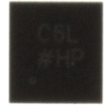
AD7156 OUTLINE DIMENSIONS 0.30 3.00 0.23 0.50 BSC BSC SQ 0.18 6 10 PIN 1 IANRDEEAX *EXPPAODSED 11..7644 (BOTTOM VIEW) 0.50 1.49 0.40 0.30 5 1 PIN 1 INDICATOR TOP VIEW 2.48 (R 0.20) 2.38 0.80 MAX 0.80 0.55 NOM 2.23 0.75 0.05 MAX 0.70 0.02 NOM SEATING PLANE 0.20 REF *FOTOHFER T PHPIIRNSO DCPAOETNRAF C ISGOHUNERNEAETTC.ITOINO NA NODF FTUHNEC ETXIOPON SDEEDS CPRAIDP TPILOENASS SEE RCETFIOERN TO 031208-B Figure 52. 10-Lead Lead Frame Chip Scale Package [LFCSP_WD] 3 mm × 3 mm Body, Very Thin, Dual Lead (CP-10-9) Dimensions shown in millimeters ORDERING GUIDE Model Temperature Range Package Description Package Option Branding AD7156BCPZ-REEL1 −40°C to +85°C 10-Lead Lead Frame Chip Scale Package [LFCSP_WD] CP-10-9 C6L AD7156BCPZ-REEL71 −40°C to +85°C 10-Lead Lead Frame Chip Scale Package [LFCSP_WD] CP-10-9 C6L EVAL-AD7156EBZ1 Evaluation Board 1 Z = RoHS Compliant Part. Rev. 0 | Page 27 of 28
AD7156 NOTES Purchase of licensed I2C components of Analog Devices or one of its sublicensed Associated Companies conveys a license for the purchaser under the Philips I2C Patent Rights to use these components in an I2C system, provided that the system conforms to the I2C Standard Specification as defined by Philips. ©2008 Analog Devices, Inc. All rights reserved. Trademarks and registered trademarks are the property of their respective owners. D07726-0-10/08(0) Rev. 0 | Page 28 of 28