ICGOO在线商城 > 集成电路(IC) > 线性 - 放大器 - 仪表,运算放大器,缓冲器放大器 > AD623BRZ
 Datasheet下载
- 型号: AD623BRZ
- 制造商: Analog
- 库位|库存: xxxx|xxxx
- 要求:
| 数量阶梯 | 香港交货 | 国内含税 |
| +xxxx | $xxxx | ¥xxxx |
查看当月历史价格
查看今年历史价格
AD623BRZ产品简介:
ICGOO电子元器件商城为您提供AD623BRZ由Analog设计生产,在icgoo商城现货销售,并且可以通过原厂、代理商等渠道进行代购。 AD623BRZ价格参考。AnalogAD623BRZ封装/规格:线性 - 放大器 - 仪表,运算放大器,缓冲器放大器, 仪表 放大器 1 电路 满摆幅 8-SOIC。您可以下载AD623BRZ参考资料、Datasheet数据手册功能说明书,资料中有AD623BRZ 详细功能的应用电路图电压和使用方法及教程。
AD623BRZ 是由 Analog Devices Inc. 生产的一款高精度、低功耗的仪表放大器,广泛应用于需要高增益精度和低噪声特性的场合。以下是其主要应用场景:

 1. 医疗设备
   AD623BRZ 在医疗设备中有着重要的应用,尤其是在心电图(ECG)、脑电图(EEG)等生物电信号测量中。这些信号通常非常微弱且容易受到外界干扰,AD623BRZ 的高共模抑制比(CMRR)和低噪声特性使其能够准确地放大这些微弱信号,同时有效抑制环境中的噪声干扰。

 2. 传感器信号调理
   在工业自动化和物联网(IoT)领域,传感器信号调理是关键环节。AD623BRZ 可以用于温度、压力、加速度等传感器的信号调理电路中,将传感器输出的微弱信号进行放大和滤波处理,确保后续数据采集系统的准确性。它支持单电源供电,适合电池供电的应用场景,如便携式传感器设备。

 3. 音频信号处理
   AD623BRZ 也可以用于音频信号处理领域,特别是在麦克风前置放大器中。它的低失真和低噪声特性使得它能够在不引入额外噪声的情况下,有效地放大音频信号,适用于高质量音频设备的设计。

 4. 精密测量仪器
   在精密测量仪器中,如万用表、示波器等,AD623BRZ 可以用于前端信号放大电路。它的高增益精度和稳定性确保了测量结果的准确性,特别适用于对精度要求极高的场合。

 5. 电力监控系统
   在电力监控系统中,AD623BRZ 可以用于电流、电压信号的精确测量。它能够有效地放大小信号,并且具有良好的线性度,确保电力参数的准确监测,适用于智能电网、能源管理系统等。

 6. 通信设备
   在通信设备中,AD623BRZ 可以用于接收端的信号放大,尤其是在射频(RF)和中频(IF)信号处理中。它的低噪声和高增益特性有助于提高通信系统的信噪比,确保信号传输的可靠性。

总之,AD623BRZ 凭借其高精度、低噪声、低功耗等特性,广泛应用于各种需要高精度信号放大的场合,尤其适合对噪声敏感的微弱信号处理。
| 参数 | 数值 |
| -3db带宽 | 800kHz |
| 产品目录 | 集成电路 (IC)半导体 |
| 描述 | IC OPAMP INSTR 800KHZ RRO 8SOIC仪表放大器 SINGLE SUPPLY RR |
| 产品分类 | Linear - Amplifiers - Instrumentation, OP Amps, Buffer Amps集成电路 - IC |
| 品牌 | Analog Devices |
| 产品手册 | |
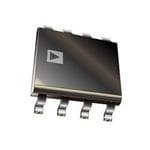
| 产品图片 |
|
| rohs | 符合RoHS无铅 / 符合限制有害物质指令(RoHS)规范要求 |
| 产品系列 | 放大器 IC,仪表放大器,Analog Devices AD623BRZ- |
| 数据手册 | |
| 产品型号 | AD623BRZ |
| PCN设计/规格 | |
| 产品培训模块 | http://www.digikey.cn/PTM/IndividualPTM.page?site=cn&lang=zhs&ptm=25193http://www.digikey.cn/PTM/IndividualPTM.page?site=cn&lang=zhs&ptm=30008http://www.digikey.cn/PTM/IndividualPTM.page?site=cn&lang=zhs&ptm=26202 |
| 产品目录页面 | |
| 产品种类 | 仪表放大器 |
| 供应商器件封装 | 8-SOIC N |
| 共模抑制比—最小值 | 105 dB |
| 包装 | 管件 |
| 压摆率 | 0.3 V/µs |
| 双重电源电压 | 2.5 V to 6 V |
| 可用增益调整 | 1 V/V to 1000 V/V |
| 商标 | Analog Devices |
| 增益带宽积 | - |
| 安装类型 | 表面贴装 |
| 安装风格 | SMD/SMT |
| 封装 | Tube |
| 封装/外壳 | 8-SOIC(0.154",3.90mm 宽) |
| 封装/箱体 | SOIC-8 |
| 工作温度 | -40°C ~ 85°C |
| 工作温度范围 | - 40 C to + 85 C |
| 工作电源电压 | 2.7 V to 12 V |
| 工厂包装数量 | 98 |
| 带宽 | 800 kHz |
| 放大器类型 | 仪表 |
| 最大功率耗散 | 650 mW |
| 最大工作温度 | + 85 C |
| 最小工作温度 | - 40 C |
| 标准包装 | 98 |
| 电压-电源,单/双 (±) | 2.7 V ~ 12 V, ± 2.5 V ~ 6 V |
| 电压-输入失调 | 25µV |
| 电流-电源 | 375µA |
| 电流-输入偏置 | 17nA |
| 电流-输出/通道 | - |
| 电源电流 | 375 uA, 305 uA |
| 电路数 | 1 |
| 系列 | AD623 |
| 视频文件 | http://www.digikey.cn/classic/video.aspx?PlayerID=1364138032001&width=640&height=505&videoID=2245193153001http://www.digikey.cn/classic/video.aspx?PlayerID=1364138032001&width=640&height=505&videoID=2245193159001 |
| 转换速度 | 0.3 V/us |
| 输入偏压电流—最大 | 25 nA |
| 输入补偿电压 | 25 uV |
| 输出类型 | 满摆幅 |
| 通道数量 | 1 Channel |


- 商务部:美国ITC正式对集成电路等产品启动337调查
- 曝三星4nm工艺存在良率问题 高通将骁龙8 Gen1或转产台积电
- 太阳诱电将投资9.5亿元在常州建新厂生产MLCC 预计2023年完工
- 英特尔发布欧洲新工厂建设计划 深化IDM 2.0 战略
- 台积电先进制程称霸业界 有大客户加持明年业绩稳了
- 达到5530亿美元!SIA预计今年全球半导体销售额将创下新高
- 英特尔拟将自动驾驶子公司Mobileye上市 估值或超500亿美元
- 三星加码芯片和SET,合并消费电子和移动部门,撤换高东真等 CEO
- 三星电子宣布重大人事变动 还合并消费电子和移动部门
- 海关总署:前11个月进口集成电路产品价值2.52万亿元 增长14.8%


PDF Datasheet 数据手册内容提取
Single and Dual-Supply, Rail-to-Rail, Low Cost Instrumentation Amplifier Data Sheet AD623 FEATURES GENERAL DESCRIPTION Easy to use The AD623 is an integrated, single- or dual-supply instrumentation Rail-to-rail output swing amplifier that delivers rail-to-rail output swing using supply Input voltage range extends 150 mV below ground voltages from 3 V to 12 V. The AD623 offers superior user (single supply) flexibility by allowing single gain set resistor programming and by Low power, 550 µA maximum supply current conforming to the 8-lead industry standard pinout configuration. Gain set with one external resistor With no external resistor, the AD623 is configured for unity Gain range: 1 to 1000 gain (G = 1), and with an external resistor, the AD623 can be High accuracy dc performance programmed for gains of up to 1000. 0.10% gain accuracy (G = 1) The superior accuracy of the AD623 is the result of increasing 0.35% gain accuracy (G > 1) ac common-mode rejection ratio (CMRR) coincident with Noise: 35 nV/√Hz RTI noise at 1 kHz increasing gain; line noise harmonics are rejected due to Excellent dynamic specifications constant CMRR up to 200 Hz. The AD623 has a wide input 800 kHz bandwidth (G = 1) common-mode range and amplifies signals with common- 20 µs settling time to 0.01% (G = 10) mode voltages as low as 150 mV below ground. The AD623 APPLICATIONS maintains superior performance with dual and single polarity Low power medical instrumentation power supplies. Transducer interfaces Table 1. Low Power Upgrades for the AD623 Thermocouple amplifiers Part No. Total V (V dc) Typical I (µA) S Q Industrial process controls AD8235 5.5 30 Difference amplifiers AD8236 5.5 33 Low power data acquisition AD8237 5.5 33 AD8226 36 350 AD8227 36 325 AD8420 36 85 AD8422 36 300 AD8426 36 325 (per channel) FUNCTIONAL BLOCK DIAGRAM +VS 2 7 –IN 50kΩ 50kΩ VDIFF– A1 2 + –RG 50kΩ VCM VDIFF– RG 81 50kΩ A3 6OUTPUT 2 + +RG +IN 3 4–VS A2 50kΩ 50kΩ 5REF 00778-054 Figure 1. Rev. F Document Feedback Information furnished by Analog Devices is believed to be accurate and reliable. However, no responsibility is assumed by Analog Devices for its use, nor for any infringements of patents or other One Technology Way, P.O. Box 9106, Norwood, MA 02062-9106, U.S.A. rights of third parties that may result from its use. Specifications subject to change without notice. No license is granted by implication or otherwise under any patent or patent rights of Analog Devices. Tel: 781.329.4700 ©1997–2018 Analog Devices, Inc. All rights reserved. Trademarks and registered trademarks are the property of their respective owners. Technical Support www.analog.com
AD623 Data Sheet TABLE OF CONTENTS Features .............................................................................................. 1 Applications Information .............................................................. 18 Applications ....................................................................................... 1 Basic Connection ....................................................................... 18 General Description ......................................................................... 1 Gain Selection ............................................................................. 18 Functional Block Diagram .............................................................. 1 Reference Terminal .................................................................... 18 Revision History ............................................................................... 2 Input and Output Offset Voltage Error ................................... 19 Input Protection ......................................................................... 19 Specifications ..................................................................................... 3 RF Interference ........................................................................... 19 Single Supply ................................................................................. 3 Grounding ................................................................................... 20 Dual Supplies ................................................................................ 5 Input Differential and Common-Mode Range vs. Specifications Common to Dual and Single Supplies ............. 7 Supply and Gain ......................................................................... 22 Absolute Maximum Ratings ............................................................ 8 Additional Information ............................................................. 23 ESD Caution .................................................................................. 8 Evaluation Board ............................................................................ 24 Pin Configuration and Function Descriptions ............................. 9 General Description ................................................................... 24 Typical Performance Characteristics ........................................... 10 Outline Dimensions ....................................................................... 25 Theory of Operation ...................................................................... 17 Ordering Guide .......................................................................... 26 REVISION HISTORY 4/2018—Rev. E to Rev. F Changes to Figure 21 Caption through Figure 26 Caption ...... 12 Changes to Gain Error Parameter, Nonlinearity Parameter, Changes to Figure 27 Caption and Figure 28 Caption .............. 13 Offset Referred to the Input vs. Supply (PSR) Parameter, and Changes to Theory of Operation Section.................................... 17 Output Swing Parameter, Table 2 ................................................... 3 Changes to Basic Connection Section ......................................... 18 Changes to Gain Error Parameter and Offset Referred to the Changes to Input and Output Offset Voltage Error Section, and Input vs. Supply (PSR) Parameter, Table 3 .................................... 5 Input Protection Section ................................................................ 19 Changes to Current Noise Parameter, Table 4 .............................. 7 Added Additional Information Section ...................................... 23 Changes to Ordering Guide .......................................................... 26 Added Evaluation Board Section and Figure 56 ........................ 24 Updated Outline Dimensions ....................................................... 25 6/2016—Rev. D to Rev. E Changes to Ordering Guide .......................................................... 26 Changes to Features Section, General Description Section, and Figure 1 ....................................................................................... 1 7/2008—Rev. C to Rev. D Deleted Connection Diagram Section ........................................... 1 Updated Format .................................................................. Universal Added Functional Block Diagram Section and Table 1; Changes to Features Section and General Description Section .. 1 Renumbered Sequentially ................................................................ 1 Changes to Table 3 ............................................................................. 6 Changes to Single Supply Section ................................................... 3 Changes to Figure 40 ...................................................................... 14 Changes to Table 3 ............................................................................ 6 Changes to Theory of Operation Section.................................... 15 Changed Both Dual and Single Supplies Section to Changes to Figure 42 and Figure 43............................................. 16 Specifications Common to Dual and Single Supplies Section ... 7 Changes to Table 7 .......................................................................... 19 Changes to Table 5 ............................................................................ 8 Updated Outline Dimensions ....................................................... 22 Added Pin Configuration and Function Descriptions Section, Changes to Ordering Guide .......................................................... 23 Figure 2, and Table 6; Renumbered Sequentially ......................... 9 Changes to Figure 5 Caption, Figure 6 Caption, and 9/1999—Rev. B to Rev. C Figure 8 Caption ............................................................................. 10 Changes to Figure 17 Caption through Figure 20 Caption ....... 11 Rev. F | Page 2 of 26
Data Sheet AD623 SPECIFICATIONS SINGLE SUPPLY Typical at 25°C, single supply, +V = 5 V, −V = 0 V, and R = 10 kΩ, unless otherwise noted. S S L Table 2. Test Conditions/ AD623A AD623ARM AD623B Parameter Comments Min Typ Max Min Typ Max Min Typ Max Unit GAIN G = 1 + (100 k/R ) G Gain Range 1 1000 1 1000 1 1000 Gain Error1 G1 V = OUT 0.15 V to 3.5 V G > 1 V = OUT 0.15 V to 4.5 V G = 1 0.03 0.10 0.03 0.10 0.03 0.05 % G = 10 0.10 0.35 0.10 0.35 0.10 0.35 % G = 100 0.10 0.35 0.10 0.35 0.10 0.35 % G = 1000 0.10 0.35 0.10 0.35 0.10 0.35 % Nonlinearity G1 V = OUT 0.15 V to 3.5 V G > 1 V = OUT 0.15 V to 4.5 V G = 1 to 1000 50 50 50 ppm Gain vs. Temperature G = 1 5 10 5 10 5 10 ppm/°C G > 11 50 50 50 ppm/°C VOLTAGE OFFSET Total RTI error = V + V /G OSI OSO Input Offset, V 25 200 200 500 25 100 µV OSI Over Temperature 350 650 160 µV Average Temperature 0.1 2 0.1 2 0.1 1 µV/°C Coefficient (Tempco) Output Offset, V 200 1000 500 2000 200 500 µV OSO Over Temperature 1500 2600 1100 µV Average Tempco 2.5 10 2.5 10 2.5 10 µV/°C Offset Referred to the Input vs. Supply (PSR) G = 1 80 100 80 100 80 100 dB G = 10 100 120 100 120 100 120 dB G = 100 100 130 100 130 100 130 dB G = 1000 100 130 100 130 100 130 dB INPUT CURRENT Input Bias Current 17 25 17 25 17 25 nA Over Temperature 27.5 27.5 27.5 nA Average Tempco 25 25 25 pA/°C Input Offset Current 0.25 2 0.25 2 0.25 2 nA Over Temperature 2.5 2.5 2.5 nA Average Tempco 5 5 5 pA/°C INPUT Input Impedance Differential 2||2 2||2 2||2 GΩ||pF Common-Mode 2||2 2||2 2||2 GΩ||pF Input Voltage Range2 V = 3 V to 12 V (−V) − (+V) − (−V) − (+V) − (−V) − (+V) − V S S S S S S S 0.15 1.5 0.15 1.5 0.15 1.5 Rev. F | Page 3 of 26
AD623 Data Sheet Test Conditions/ AD623A AD623ARM AD623B Parameter Comments Min Typ Max Min Typ Max Min Typ Max Unit Common-Mode Rejection at 60 Hz with 1 kΩ Source Imbalance G = 1 V = 0 V to 3 V 70 80 70 80 77 86 dB CM G = 10 V = 0 V to 3 V 90 100 90 100 94 100 dB CM G = 100 V = 0 V to 3 V 105 110 105 110 105 110 dB CM G = 1000 V = 0 V to 3 V 105 110 105 110 105 110 dB CM OUTPUT Output Swing R = 10 kΩ 0.2 (+V) − 0.2 (+V) − 0.2 (+V) − V L S S S 0.5 0.5 0.5 R = 100 kΩ 0.05 (+V) − 0.05 (+V) − 0.05 (+V) − V L S S S 0.15 0.15 0.15 DYNAMIC RESPONSE Small Signal −3 dB BW G = 1 800 800 800 kHz G = 10 100 100 100 kHz G = 100 10 10 10 kHz G = 1000 2 2 2 kHz Slew Rate 0.3 0.3 0.3 V/µs Settling Time to 0.01% V = 5 V S G = 1 Step size: 3.5 V 30 30 30 µs G = 10 Step size: 4 V, 20 20 20 µs V = 1.8 V CM 1 Does not include effects of external resistor, RG. 2 One input grounded. G = 1. Rev. F | Page 4 of 26
Data Sheet AD623 DUAL SUPPLIES Typical at 25°C dual supply, V = ±5 V, and R = 10 kΩ, unless otherwise noted. S L Table 3. Test Conditions/ AD623A AD623ARM AD623B Parameter Comments Min Typ Max Min Typ Max Min Typ Max Unit GAIN G = 1 + (100 k/R ) G Gain Range 1 1000 1 1000 1 1000 Gain Error1 G1 V = OUT −4.8 V to +3.5 V G > 1 V = OUT −4.8 V to 4.5 V G = 1 0.03 0.10 0.03 0.10 0.03 0.05 % G = 10 0.10 0.35 0.10 0.35 0.10 0.35 % G = 100 0.10 0.35 0.10 0.35 0.10 0.35 % G = 1000 0.10 0.35 0.10 0.35 0.10 0.35 % Nonlinearity G1 V = OUT −4.8 V to +3.5 V G > 1 V = OUT −4.8 V to +4.5 V G = 1 to 1000 50 50 50 ppm Gain vs. Temperature G = 1 5 10 5 10 5 10 ppm/°C G > 11 50 50 50 ppm/°C VOLTAGE OFFSET Total RTI error = V + V /G OSI OSO Input Offset, V 25 200 200 500 25 100 µV OSI Over Temperature 350 650 160 µV Average Tempco 0.1 2 0.1 2 0.1 1 µV/°C Output Offset, V 200 1000 500 2000 200 500 µV OSO Over Temperature 1500 2600 1100 µV Average Tempco 2.5 10 2.5 10 2.5 10 µV/°C Offset Referred to the Input vs. Supply (PSR) G = 1 80 100 80 100 80 100 dB G = 10 100 120 100 120 100 120 dB G = 100 100 130 100 130 100 130 dB G = 1000 100 130 100 130 100 130 dB INPUT CURRENT Input Bias Current 17 25 17 25 17 25 nA Over Temperature 27.5 27.5 27.5 nA Average Tempco 25 25 25 pA/°C Input Offset Current 0.25 2 0.25 2 0.25 2 nA Over Temperature 2.5 2.5 2.5 nA Average Tempco 5 5 5 pA/°C INPUT Input Impedance Differential 2||2 2||2 2||2 GΩ||pF Common-Mode 2||2 2||2 2||2 GΩ||pF Input Voltage Range2 V = (−V) – (+V) – (−V) – (+V) – (−V) – (+V) – V S S S S S S S +2.5 V to ±6 V 0.15 1.5 0.15 1.5 0.15 1.5 Rev. F | Page 5 of 26
AD623 Data Sheet Test Conditions/ AD623A AD623ARM AD623B Parameter Comments Min Typ Max Min Typ Max Min Typ Max Unit Common-Mode Rejection at 60 Hz with 1 kΩ Source Imbalance G = 1 V = 70 80 70 80 77 86 dB CM +3.5 V to −5.15 V G = 10 V = 90 100 90 100 94 100 dB CM +3.5 V to −5.15 V G = 100 V = 105 110 105 110 105 110 dB CM +3.5 V to −5.15 V G = 1000 V = 105 110 105 110 105 110 dB CM +3.5 V to −5.15 V OUTPUT Output Swing R = 10 kΩ, (−V) + (+V) − (−V) + (+V) − (−V) + (+V) − V L S S S S S S V = ±5 V 0.2 0.5 0.2 0.5 0.2 0.5 S R = 100 kΩ (−V) + (+V) − (−V) + (+V) − (−V) + (+V) − V L S S S S S S 0.05 0.15 0.05 0.15 0.05 0.15 DYNAMIC RESPONSE Small Signal −3 dB Bandwidth G = 1 800 800 800 kHz G = 10 100 100 100 kHz G = 100 10 10 10 kHz G = 1000 2 2 2 kHz Slew Rate 0.3 0.3 0.3 V/µs Settling Time to 0.01% V = ±5 V, 5 V step S G = 1 30 30 30 µs G = 10 20 20 20 µs 1 Does not include effects of external resistor, RG. 2 One input grounded. G = 1. Rev. F | Page 6 of 26
Data Sheet AD623 SPECIFICATIONS COMMON TO DUAL AND SINGLE SUPPLIES Table 4. Test Conditions/ AD623A AD623ARM AD623B Parameter Comments Min Typ Max Min Typ Max Min Typ Max Unit NOISE Voltage Noise, 1 kHz Total RTI noise = (e )2+(2e /G)2 ni no Input, Voltage Noise, e 35 35 35 nV/√Hz ni Output, Voltage Noise, e 50 50 50 nV/√Hz no RTI, 0.1 Hz to 10 Hz G = 1 3.0 3.0 3.0 µV p-p G = 1000 1.5 1.5 1.5 µV p-p Current Noise f = 1 kHz 100 100 100 fA/√Hz 0.1 Hz to 10 Hz 2.5 2.5 2.5 pA p-p REFERENCE INPUT R 100 ± 100 ± 100 ± kΩ IN 20% 20% 20% I V +, V = 0 V 50 60 50 60 50 60 µA IN IN REF Voltage Range −V +V −V +V −V +V V S S S S S S Gain to Output 1 ± 1 ± 1 ± V 0.0002 0.0002 0.0002 POWER SUPPLY Operating Range Dual supply ±2.5 ±6 ±2.5 ±6 ±2.5 ±6 V Single supply 2.7 12 2.7 12 2.7 12 V Quiescent Current Dual supply 375 550 375 550 375 550 µA Single supply 305 480 305 480 305 480 µA Over Temperature 625 625 625 µA TEMPERATURE RANGE For Specified Performance −40 +85 −40 +85 −40 +85 °C Rev. F | Page 7 of 26
AD623 Data Sheet ABSOLUTE MAXIMUM RATINGS Table 5. Stresses at or above those listed under Absolute Maximum Parameter Rating Ratings may cause permanent damage to the product. This is a Supply Voltage 12 V stress rating only; functional operation of the product at these Internal Power Dissipation1 650 mW or any other conditions above those indicated in the operational Differential Input Voltage ±6 V section of this specification is not implied. Operation beyond Output Short-Circuit Duration Indefinite the maximum operating conditions for extended periods may Storage Temperature Range −65°C to +125°C affect product reliability. Operating Temperature Range −40°C to +85°C ESD CAUTION Lead Temperature (Soldering, 10 sec) 300°C 1 Specification is for device in free air: 8-Lead PDIP Package: θJA = 95°C/W 8-Lead SOIC Package: θJA = 155°C/W 8-Lead MSOP Package: θJA = 200°C/W Rev. F | Page 8 of 26
Data Sheet AD623 PIN CONFIGURATION AND FUNCTION DESCRIPTIONS AD623 –RG 1 8 +RG –IN 2 7 +VS +IN 3 6 OUTPUT –VS 4 5 REF (NToOt Pto V SIEcaWle) 00778-001 Figure 2. AD623 Pin Configuration Table 6. Pin Function Descriptions Pin No. Mnemonic Description 1 −R Inverting Terminal of External Gain-Setting Resistor, R . G G 2 −IN Inverting In-Amp Input. 3 +IN Noninverting In-Amp Input. 4 −V Negative Supply Terminal. S 5 REF In-Amp Output Reference Input. The voltage input establishes the common-mode voltage of the output. 6 OUTPUT In-Amp Output. 7 +V Positive Supply Terminal. S 8 +R Noninverting Terminal of External Gain Setting Resistor, R . G G Rev. F | Page 9 of 26
AD623 Data Sheet TYPICAL PERFORMANCE CHARACTERISTICS At 25°C, V = ±5 V, and R = 10 kΩ, unless otherwise noted. S L 300 22 280 260 20 240 18 220 16 200 180 14 TS 160 TS 12 UNI 140 UNI 10 120 100 8 80 6 60 4 40 20 2 –0100–80 –60 –40INP–2U0T O0FFSE20T VO40LTA6G0E (µ8V0) 100 120 140 00778-003 0 –600–500–400O–U3T0P0U–T2 O00FF–S10E0T VO0LTA10G0E (2µ0V0) 300 400 500 00778-006 Figure 3. Typical Distribution of Input Offset Voltage, Figure 6. Typical Distribution of Output Offset Voltage, N-8 and R-8 Package Options +VS = 5 V, −VS = 0 V, VREF = −0.125 V, N-8 and R-8 Package Options 480 210 420 180 360 150 300 UNITS 240 UNITS 120 90 180 60 120 60 30 0 –800 –600 O–4U0T0PU–T2 0O0FFSE0T VO2L0T0AGE4 0(0µV) 600 800 00778-004 0 –0.245 –0.240IN–P0U.2T3 O5FF–0S.E2T30 CU–R0R.2E2N5T –(0n.A2)20 –0.215 –0.210 00778-007 Figure 4. Typical Distribution of Output Offset Voltage, Figure 7. Typical Distribution for Input Offset Current, N-8 and R-8 Package Options N-8 and R-8 Package Options 22 20 20 18 18 16 16 14 14 UNITS 1120 UNITS 1120 8 8 6 6 4 4 2 2 0 –80 –60 I–N4P0UT –O2F0FSE0T VOL20TAGE4 0(µV)60 80 100 00778-005 –00.025 –0.020 –0.0IN15PU–T0 O.0F1F0SE–0T. 0C0U5RREN0T (nA0).005 0.010 00778-008 Figure 5. Typical Distribution of Input Offset Voltage, Figure 8. Typical Distribution for Input Offset Current, +VS = 5 V, −VS = 0 V, VREF = −0.125 V, N-8 and R-8 Package Options +VS = 5 V, −VS = 0 V, VREF = −0.125 V, N-8 and R-8 Package Options Rev. F | Page 10 of 26
Data Sheet AD623 1600 30 1400 25 1200 20 1000 UNITS 800 (nA)BIAS 15 I 600 10 400 5 200 0 0 75 80 85 90 95 C1M0R0R1 (0d5B)110 115 120 125 130 00778-009 –60 –40 –20 0 TE2M0PERA40TURE6 0(°C) 80 100 120 140 00778-012 Figure 9. Typical Distribution for CMRR (G = 1) Figure 12. IBIAS vs. Temperature DENSITY (nV/ Hz RTI) 1k L DENSITY (fA/ Hz) 1k SPECTRAL 100 G = 1 E SPECTRA 100 NOISE G= 10 T NOIS GE G= 100 REN A R OLT G= 1000 CU V 101 10 F1R0E0QUENCY (1Hkz) 10k 100k 00778-010 101 10FREQUENCY (Hz)100 1k 00778-013 Figure 10. Voltage Noise Spectral Density vs. Frequency Figure 13. Current Noise Spectral Density vs. Frequency 22 20.0 21 19.5 20 19.0 19 18.5 A) A) I (nBIAS 1178 I (nBIAS 1178..50 16 17.0 15 16.5 14 –4 –2 CMV (V) 0 2 4 00778-011 16.0–4 –3 –2 CM–V1 (V) 0 1 2 00778-014 Figure 11. IBIAS vs. CMV Figure 14. IBIAS vs. CMV, VS = ±2.5 V Rev. F | Page 11 of 26
AD623 Data Sheet 120 CH1 10mV A 1s 100mV VERT 110 100 G = ×1000 90 dB) 80 R ( G = ×100 M 70 C 60 G = ×10 50 00778-015 3400 G = ×1 1 10 1F0R0EQUENC1Yk (Hz) 10k 100k 00778-018 Figure 15. 0.1 Hz to 10 Hz Current Noise (0.71 pA/DIV) Figure 18. CMR vs. Frequency for Various Gain Settings (G) 70 1µV/DIV 1s G = 1000 60 50 G = 100 40 B) 30 N (d 20 G = 10 AI G 10 G = 1 0 –10 00778-016 ––3200 100 1k FREQU1E0NkCY (Hz) 100k 1M 00778-019 Figure 16. 0.1 Hz to 10 Hz RTI Voltage Noise (1 DIV = 1 µV p-p) Figure 19. Gain vs. Frequency (+VS = 5 V, −VS = 0 V), VREF = 2.5 V, for Various Gain Settings (G) 120 5 4 110 3 100 G = ×1000 T (V) 2 90 G = ×100 NPU 1 VS = ±2.5V R (dB) 80 ODE I 0 CM 70 N-M –1 60 G = ×10 MMO –2 O –3 C 50 –4 G = ×1 40 –5 301 10 1F0R0EQUENC1Yk (Hz) 10k 100k 00778-017 –6–5 –4 –3MA–X2IMUM– 1OUTP0UT VO1LTAG2E (V) 3 4 5 00778-020 Figure 17. Common-Mode Rejection (CMR) vs. Frequency, +VS = 5 V, − VS = 0 Figure 20. Maximum Output Voltage vs. Common-Mode Input, V, VREF = 2.5 V, for Various Gain Settings (G) G = 1, RL = 100 kΩ for Two Supply Voltages Rev. F | Page 12 of 26
Data Sheet AD623 5 140 4 120 3 G = 1000 NPUT (V) 12 VS = ±2.5V R (dB) 100 G = 100 DE I 0 PSS 80 N-MO –1 TIVE 60 MO –2 OSI G = 10 OM –3 P 40 C G = 1 –4 20 –5 –6 0 –5 –4 –3MA–X2IMUM– 1OUTP0UT VO1LTAG2E (V) 3 4 5 00778-021 1 10 F1R0E0QUENCY (1Hkz) 10k 100k 00778-024 Figure 21. Maximum Output Voltage vs. Common-Mode Input, Figure 24. Positive PSRR vs. Frequency G ≥ 10, RL = 100 Ω, for Two Supply Voltages 5 140 120 4 G = 1000 V) NPUT ( 3 R (dB) 100 G = 100 N-MODE I 2 TIVE PSS 8600 OMMO 1 POSI 40 G = 10 C G = 1 0 20 –1 0 0 1 MAXIMUM2 OUTPUT VO3LTAGE (V) 4 5 00778-022 1 10 F1R0E0QUENCY (1Hkz) 10k 100k 00778-025 Figure 22. Maximum Output Voltage vs. Common-Mode Input, Figure 25. Positive PSRR vs. Frequency, +VS = 5V, −VS = 0 V, G = 1, +VS = 5 V, −VS = 0 V, RL = 100 kΩ for Various Gain Settings (G) 5 140 120 G = 1000 4 G = 100 ODE INPUT (V) 23 E PSRR (dB) 10800 G = 10 ON-M GATIV 60 G = 1 OMM 1 NE 40 C 0 20 –10 1 MAXIMUM2 OUTPUT VO3LTAGE (V) 4 5 00778-023 01 10 F1R0E0QUENCY (1Hkz) 10k 100k 00778-026 Figure 23. Maximum Output Voltage vs. Common-Mode Input, Figure 26. Negative PSRR vs. Frequency for Various Gain Settings (G) G ≥ 10, +VS = 5 V, −VS = 0 V, RL = 100 kΩ Rev. F | Page 13 of 26
AD623 Data Sheet 10 500µV 1V 10µs 8 p) p- V GE ( 6 A T L O V T 4 U TP VS = ±5V U O VS = ±2.5V 2 0 00778-030 0 20 FR4E0QUENCY (k6H0z) 80 100 00778-027 Figure 27. Large Signal Response, G ≤ 10 for Two Supply Voltages Figure 30. Large Signal Pulse Response and Settling Time, G = −10 (0.250 mV = 0.01%), CL = 100 pF 1k 10mV 2V 50µs µs) 100 E ( M TI G N LI T T E 10 S 1 00778-031 1 10 GAIN (V/V) 100 1k 00778-028 Figure 28. Settling Time to 0.01% vs. Gain, for a 5 V Step at Output, Figure 31. Large Signal Pulse Response and Settling Time, CL = 100 pF G = 100, CL = 100 pF 500µV 1V 20µs 20mV 2V 500µs 00778-029 00778-032 Figure 29. Large Signal Pulse Response and Settling Time, Figure 32. Large Signal Pulse Response and Settling Time, G = −1 (0.250 mV = 0.01%), CL = 100 pF G = −1000 (5 mV = 0.01%), CL = 100 pF Rev. F | Page 14 of 26
Data Sheet AD623 20mV 2µs 20mV 500µs 00778-033 00778-036 Figure 33. Small Signal Pulse Response, G = 1, RL = 10 kΩ, CL = 100 pF Figure 36. Small Signal Pulse Response, G = 1000, RL = 10 kΩ, CL = 100 pF 20mV 5µs 200µV 00778-034 1V 00778-037 Figure 34. Small Signal Pulse Response, G = 10, RL = 10 kΩ, CL = 100 pF Figure 37. Gain Nonlinearity, G = −1 (50 ppm/DIV) 20mV 50µs 20µV 1V 00778-035 00778-038 Figure 35. Small Signal Pulse Response, G = 100, RL = 10 kΩ, CL = 100 pF Figure 38. Gain Nonlinearity, G = −10 (6 ppm/DIV) Rev. F | Page 15 of 26
AD623 Data Sheet V+ 50µV 1V V) (V+) –0.5 G ( N WI E S (V+) –1.5 G A T L O V (V+) –2.5 T U P T U O (V–) +0.5 00778-039 V– 0 0.5 OUTPUT CU1.R0RENT (mA) 1.5 2.0 00778-040 Figure 39. Gain Nonlinearity, G = −100, 15 ppm/DIV Figure 40. Output Voltage Swing vs. Output Current Rev. F | Page 16 of 26
Data Sheet AD623 THEORY OF OPERATION The AD623 is an instrumentation amplifier based on a modified The output voltage at Pin 6 is measured with respect to the classic 3-op-amp approach, to assure single- or dual-supply potential at Pin 5. The impedance of the reference pin is 100 kΩ; operation even at common-mode voltages at the negative supply therefore, in applications requiring voltage conversion, a small rail. Low voltage offsets, input and output, as well as absolute resistor between Pin 5 and Pin 6 is all that is needed. gain accuracy, and one external resistor to set the gain, make +VS the AD623 one of the most versatile instrumentation amplifiers 7 in its class. The input signal is applied to PNP transistors acting as voltage –IN 2 buffers and providing a common-mode signal to the input 4 amplifiers (see Figure 41). An absolute value 50 kΩ resistor in –RG 1 –VS 50kΩ 50kΩ 50kΩ each amplifier feedback assures gain programmability. 6 RG OTUPUT The differential output is V =1+100kΩV +RG 8 +VS 50kΩ 50kΩ 50kΩ 5 REF O R C 7 G The differential voltage is then converted to a single-ended 3 +IN vcoomltamgeo nus-mingo dthe es ioguntaplu att atmhep oliufitepru, tw ohfi cthhe a ilnsop uret jaemctps laifniyer s. –VS4 00778-041 Because the amplifiers can swing to either supply rail, as well as Figure 41. Simplified Schematic have their common-mode range extended to below the negative Because of the voltage feedback topology of the internal op supply rail, the range over which the AD623 can operate is further amps, the bandwidth of the in-amp decreases with increasing enhanced (see Figure 20 and Figure 21). gain. At unity gain, the output amplifier limits the bandwidth. Rev. F | Page 17 of 26
AD623 Data Sheet APPLICATIONS INFORMATION BASIC CONNECTION The input voltage, which can be either single-ended (tie either −IN or +IN to ground) or differential, is amplified by the Figure 42 and Figure 43 show the basic connection circuits for programmed gain. The output signal appears as the voltage the AD623. The +V and −V terminals are connected to the S S difference between the OUTPUT pin and the externally applied power supply. The supply can be either bipolar (V = ±2.5 V to S voltage on the REF input. For a ground referenced output, REF ±6 V) or single supply (−V = 0 V, +V = 3.0 V to 12 V). S S must be grounded. Capacitively decouple power supplies close to the power pins of the device. For best results, use surface-mount 0.1 µF ceramic GAIN SELECTION chip capacitors and 10 µF electrolytic tantalum capacitors. The gain of the AD623 is programmed by the R resistor, or G +VS more precisely, by whatever impedance appears between Pin 1 0.1µF 10µF and Pin 8. The AD623 offers accurate gains using 0.1% to 1% tolerance resistors. Table 7 shows the required values of R for +2.5V TO +6V G the various gains. Note that for G = 1, the R terminals are G RG VIN RG OUTPUT VOUT unconnected (RG = ∞). For any arbitrary gain, RG can be RGREF calculated by REF (INPUT) R = 100 kΩ/(G − 1) 0.1µF 10µF G –VS–2.5V TO –6V 00778-042 RThEeF rEeRfeEreNncCeE t eTrmERinMalI pNoAteLn tial defines the zero output voltage Figure 42. Dual-Supply Basic Connection and is especially useful when the load does not share a precise +VS ground with the rest of the system. It provides a direct means of 0.1µF 10µF injecting a precise offset to the output. The reference terminal is also useful when bipolar signals are being amplified because it +3V TO +12V can be used to provide a virtual ground voltage. The voltage on RG the reference terminal can be varied from −V to +V. VIN RG OUTPUT VOUT S S RGREF REF (INPUT) 00778-055 Figure 43. Single-Supply Basic Connection Table 7. Required Values of Gain Resistors Desired Gain 1% Standard Table Value of R Calculated Gain Using 1% Resistors G 2 100 kΩ 2 5 24.9 kΩ 5.02 10 11 kΩ 10.09 20 5.23 kΩ 20.12 33 3.09 kΩ 33.36 40 2.55 kΩ 40.21 50 2.05 kΩ 49.78 65 1.58 kΩ 64.29 100 1.02 kΩ 99.04 200 499 Ω 201.4 500 200 Ω 501 1000 100 Ω 1001 Rev. F | Page 18 of 26
Data Sheet AD623 INPUT AND OUTPUT OFFSET VOLTAGE ERROR RF INTERFERENCE The offset voltage (V ) of the AD623 is attributed to two All instrumentation amplifiers can rectify high frequency out- OS sources: those originating in the two input stages where the in- of-band signals. Once rectified, these signals appear as dc offset amp gain is established, and those originating in the subtractor errors at the output. The circuit in Figure 45 provides good RFI output stage. The output error is divided by the programmed suppression without reducing performance within the pass band of gain when referred to the input. In practice, the input errors the in-amp. Resistor R1 and Capacitor C1 (and likewise, R2 and dominate at high gain settings, whereas the output error C2) form a low-pass RC filter that has a −3 dB bandwidth equal prevails when the gain is set at or near unity. to f = 1/(2 π R1C1). Using the component values shown, this filter has a −3 dB bandwidth of approximately 40 kHz. The R1 The V error for any given gain is calculated as follows: OS and R2 resistors were selected to be large enough to isolate the Total Error Referred to Input (RTI) input of the circuit from the capacitors, but not large enough to = Input Error + (Output Error/G) significantly increase the noise of the circuit. To preserve common- Total Error Referred to Output (RTO) mode rejection in the pass band of the amplifier, the C1 and C2 = (Input Error × G) + Output Error capacitors must be 5% or better units, or low cost 20% units can be tested and binned to provide closely matched devices. The RTI offset errors and noise voltages for different gains are listed in Table 8. +VS 0.33µF 0.01µF INPUT PROTECTION R1 C1 4.02kΩ 1000pF Internal supply-referenced clamping diodes allow the input, 1% 5% –IN rweiftehrsetnacned, oouvetpruvot,l taangde sg oaifn 0 .t3e rVm ainbaolvse o of rt hbee lAowD 6th23e stou pspafleielys. 4.01R2%2kΩ 0.047CµF3 RG AD623 VOUT +IN REFERENCE This overvoltage protection is true at all gain settings and when C2 cycling power on and off. Overvoltage protection is particularly 10005p%F 0.33µF 0.01µF important because the signal source and amplifier may be powered separately. N1.O LTOECSA:TE C1 TO C3 AS CLOSE TO THE IN+PVUST PINS AS POSSIBLE. 00778-044 If the overvoltage is expected to exceed this value, the current Figure 45. Circuit to Attenuate RF Interference through these diodes must be limited to about 10 mA using Capacitor C3 is needed to maintain common-mode rejection at external current limiting resistors (see Figure 44). The size of low frequencies. R1/R2 and C1/C2 form a bridge circuit whose this resistor is defined by the supply voltage and the required output appears across the input pins of the in-amp. Any mismatch overvoltage protection. between C1 and C2 unbalances the bridge and reduces the +VS common-mode rejection. C3 ensures that any RF signals are I = 10mA MAX common mode (the same on both in-amp inputs) and are not VOVER RLIM AD623 applied differentially. This second low-pass network, R1 + R2 and RG OUTPUT C3, has a −3 dB frequency equal to 1/(2π(R1 + R2)(C3)). Using VOVER RLIM –VSRLIM =VOVER1 –0VmSA + 0.7V 00778-043 aiiss Calep3sp svr atohlxuaiemn o a1ft .e05l. y0µ 44V70, 0aµ nHF,d zt .ht hTee h− eR3 tF yd psBii gcsanigla ndl car leo bjfefacsnetidto wsnhi idofttf h ot hvoeefr tc fhirriescq ucuiiert cniusc iyt Figure 44. Input Protection better than 71 dB. The 3 dB signal bandwidth of this circuit can be increased to 900 Hz by reducing R1 and R2 to 2.2 kΩ. The performance is similar to using 4 kΩ resistors, except that the circuitry preceding the in-amp must drive a lower impedance load. Table 8. RTI Error Sources Maximum Total Input Offset Error (µV) Maximum Total Input Offset Drift (µV/°C) Total Input Referred Noise (nV/√Hz) Gain AD623A AD623B AD623A AD623B AD623A AD623B 1 1200 600 12 11 62 62 2 700 350 7 6 45 45 5 400 200 4 3 38 38 10 300 150 3 2 35 35 20 250 125 2.5 1.5 35 35 50 220 110 2.2 1.2 35 35 100 210 105 2.1 1.1 35 35 1000 200 100 2 1 35 35 Rev. F | Page 19 of 26
AD623 Data Sheet The circuit in Figure 45 must be built using a printed circuit GROUNDING board (PCB) with a ground plane on both sides. All component Because the AD623 output voltage is developed with respect leads must be as short as possible. The R1 and R2 resistors can to the potential on the reference terminal, many grounding be common 1% metal film units; however, the C1 and C2 problems can be solved by simply tying the REF pin to the capacitors must be ±5% tolerance devices to avoid degrading appropriate local ground. The REF pin must, however, be tied the common-mode rejection of the circuit. Either the to a low impedance point for optimal CMR. traditional 5% silver mica units or Panasonic ±2% PPS film The use of ground planes is recommended to minimize the capacitors are recommended. impedance of ground returns (and hence the size of dc errors). In many applications, shielded cables are used to minimize noise; To isolate low level analog signals from a noisy digital environment, for best CMR over frequency, the shield must be properly driven. many data acquisition components have separate analog and digital Figure 46 shows an active guard driver that is configured to ground returns (see Figure 47). All ground pins from mixed signal improve ac common-mode rejection by bootstrapping the components, such as analog-to-digital converters (ADCs), must capacitances of input cable shields, thus minimizing the be returned through the high quality analog ground plane. capacitance mismatch between the inputs. Maximum isolation between analog and digital is achieved by +VS connecting the ground planes back at the supplies. The digital return currents from the ADC that flow in the analog ground –IN 2 plane, in general, have a negligible effect on noise performance. RG 1 7 100Ω 2 If there is only a single power supply available, it must be shared AD8031 AD623 6 OUTPUT R2G 8 5 by both digital and analog circuitry. Figure 48 shows how to 3 4 REF minimize interference between the digital and analog circuitry. +IN As in the previous case, use separate analog and digital ground Figure 46. Common-Mode S–hViSeld Driver 00778-045 pdliagniteasl g(rreoausnodn apblalyn teh).i cTkh tersaec egsr ocuann db ep luasneeds ams uanst ablete cronnatnievcet teod aa t the ground pin of the power supply. Run separate traces from the power supply to the supply pins of the digital and analog circuits. Ideally, each device has its own power supply trace, but these can be shared by a number of devices, as long as a single trace is not used to route current to both digital and analog circuitry. ANALOG POWER SUPPLY DIGITAL POWER SUPPLY +5V –5V GND GND +5V 0.1µF 0.1µF 0.1µF 0.1µF 2 7 1 6 14 4 VDD AGND DGND 12 AGND VDD AD623 6 4 VIN1 ADC MICROPROCESSOR AD7892-2 3 5 3 VIN2 00778-046 Figure 47. Optimal Grounding Practice for a Bipolar Supply Environment with Separate Analog and Digital Supplies POWER SUPPLY +5V GND 0.1µF 0.1µF 0.1µF 2 7 1 6 14 4 VDD AGND DGND 12 AGND VDD AD623 6 4 VIN1 ADC MICROPROCESSOR AD7892-2 3 5 00778-047 Figure 48. Optimal Ground Practice in a Single-Supply Environment Rev. F | Page 20 of 26
Data Sheet AD623 Ground Returns for Input Bias Currents Output Buffering Input bias currents are those dc currents that must flow to bias The AD623 is designed to drive loads of 10 kΩ or greater. If the the input transistors of an amplifier. These are usually transistor load is less than this value, the output of the AD623 must be base currents. When amplifying floating input sources, such as buffered with a precision single-supply op amp, such as the transformers or ac-coupled sources, there must be a direct dc OP113. This op amp can swing from 0 V to 4 V on its output path into each input so that the bias current can flow. Figure 49, while driving a load as small as 600 Ω. Table 9 summarizes the Figure 50, and Figure 51 show how a bias current path can be performance of some buffer op amps. provided for the cases of transformer coupling, thermocouple, 5V and capacitive ac coupling. In dc-coupled resistive bridge 0.1µF 5V applications, providing this path is generally not necessary 0.1µF because the bias current simply flows from the bridge supply through the bridge into the amplifier. However, if the impedances VIN RG AD623 that the two inputs see are large and differ by a large amount OP113 VOUT REFERENCE (p>ro10p okrΩti)o,n tahle w oiftfhse tth ceu irnrpeuntt oofff tsheet vinopltuagt es toafg eth cea uamseps ldifcie err. rors 00778-051 Figure 52. Output Buffering +VS –IN 2 Table 9. Buffering Options 7 1 Op Amp Description RG AD623 6 OUTPUT OP113 Single-supply, high output current 8 5 OP191 Rail-to-rail input and output, low supply current REF +IN 3 4 –VS LOAD TSGOURP OPPUOLNWYDER 00778-048 SInintegrflaec-iSnugp bpiplyo lDara stiag nAaclqs utoi ssiitnioglne- Ssuypstpelym A DCs presents a Figure 49. Ground Returns for Bias Currents with Transformer-Coupled Inputs challenge. The bipolar signal must be mapped into the input range of the ADC. Figure 53 shows how this translation can be +VS achieved. –IN 2 7 5V 1 5V 5V 0.1µF RG AD623 6 OTUPUT 0.1µF 8 5 REF +IN 3 4 LOAD ±10mV 1.02RkΩG AD623 AINAD7776 Figure 50. Ground Returns f–oVrS Bias Currents with ThermocTSGoOURuP OPpPUOlLeNWY IDnEpRuts00778-049 REFERENCE REFOUT REFIN –IN +VS 00778-052 2 Figure 53. A Single-Supply Data Acquisition System 7 1 The bridge circuit is excited by a 5 V supply. The full-scale output RG AD623 6 OUTPUT voltage from the bridge (±10 mV) therefore has a common-mode 8 5 REF level of 2.5 V. The AD623 removes the common-mode component 3 4 +IN and amplifies the input signal by a factor of 100 (R = 1.02 kΩ), LOAD GAIN 100kΩ 100kΩ –VS TSGOURP OPPUOLNWYDER 00778-050 wfrohmich r urensnuilntsg iinn taon tohuet gpruotu snigdn raal iol fo ±f t1h Ve .A TDo 6p2re3v, ethnet tvhoilst asgigen oanl Figure 51. Ground Returns for Bias Currents with AC-Coupled Inputs the REF pin must be raised to at least 1 V. In this example, the 2 V reference voltage from the AD7776 ADC biases the output voltage of the AD623 to 2 V ± 1 V, which corresponds to the input range of the ADC. Rev. F | Page 21 of 26
AD623 Data Sheet Amplifying Signals with Low Common-Mode Voltage equations, the maximum and minimum input common-mode voltages are given by the following equations: Because the common-mode input range of the AD623 extends 0.1 V below ground, it is possible to measure small differential V = V+ − 0.7 V − V × Gain/2 CMMAX DIFF signals that have low or no common-mode component. Figure 54 V = V− − 0.590 V + V × Gain/2 CMMIN DIFF shows a thermocouple application where one side of the J-type These equations can be rearranged to give the maximum possible thermocouple is grounded. differential voltage (positive or negative) for a particular common- 5V mode voltage, gain, and power supply. Because the signals on 0.1µF A1 and A2 can clip on either rail, the maximum differential voltage is the lesser of the two equations. THERMOCJO-UTYPPLEE 1.02RkΩG AD623 OUTPUT |V | = 2 (V+ − 0.7 V − V )/Gain DIFFMAX CM REF |V | = 2 (V − V− +0.590 V)/Gain DIFFMAX CM 2V 00778-053 However, the range on the differential input voltage range is Figure 54. Amplifying Bipolar Signals with Low Common-Mode Voltage also constrained by the output swing. Therefore, the range of V may need to be lower according the following equation: Over a temperature range of −200°C to +200°C, the J-type thermo- DIFF couple delivers a voltage ranging from −7.890 mV to +10.777 mV. Input Range ≤ Available Output Swing/Gain A programmed gain on the AD623 of 100 (RG = 1.02 kΩ) and a For a bipolar input voltage with a common-mode voltage that is voltage on the REF pin of 2 V result in the output voltage ranging roughly half way between the rails, V is half the value that DIFFMAX from 1.110 V to 3.077 V relative to ground. the previous equations yield because the REF pin is at midsupply. INPUT DIFFERENTIAL AND COMMON-MODE Note that the available output swing is given for different supply RANGE vs. SUPPLY AND GAIN conditions in the Specifications section. Figure 55 shows a simplified block diagram of the AD623. The The equations can be rearranged to give the maximum gain for voltages at the outputs of Amplifier A1 and Amplifier A2 are a fixed set of input conditions. The maximum gain is the lesser given by of the two equations. VA2 = VCM + VDIFF/2 + 0.6 V + VDIFF × RF/RG GainMAX = 2 (V+ − 0.7 V − VCM)/VDIFF = VCM + 0.6 V + VDIFF × Gain/2 GainMAX = 2 (VCM − V− +0.590 V)/VDIFF VA1 = VCM − VDIFF/2 + 0.6 V + VDIFF × RF/RG Again, it is recommended that the resulting gain times the input = VCM + 0.6 V − VDIFF × Gain/2 range is less than the available output swing. If this is not the case, +VS the maximum gain is given by 7 Gain = Available Output Swing/Input Range MAX Also for bipolar inputs (that is, input range = 2 V ), the 2 A1 DIFF –IN maximum gain is half the value yielded by the previous equations VDIFF– –VS4 1 50RkFΩ 50kΩ 50kΩ because the REF pin must be at midsupply. 2 + The maximum gain and resulting output swing for different input 6 GAIN A3 OUTPUT conditions is given in Table 10. Output voltages are referenced to VCM RG RF the voltage on the REF pin. 8 50kΩ 50kΩ 50kΩ 5 +VS REF For the purposes of computation, it is necessary to break down the VDIFF– 7 input voltage into its differential and common-mode components. 2 + A2 Therefore, when one of the inputs is grounded or at a fixed +IN 3 voltage, the common-mode voltage changes as the differential –VS4 00778-055 vFoigltuargee 5 c4h. aTnhgee si.n Tvaekrtei nthge i ncpasuet oofn t thhee t AheDrm62o3c oisu gprloeu anmdpeldif; ier in Figure 55. Simplified Block Diagram therefore, when the input voltage is −10 mV, the voltage on the The voltages on these internal nodes are critical in determining noninverting input is −10 mV. For the purpose of the signal whether the output voltage is clipped. The VA1 and VA2 voltages swing calculations, this input voltage must be composed of a can swing from approximately 10 mV above the negative supply common-mode voltage of −5 mV (that is, (+IN + −IN)/2) and (V− or ground) to within approximately 100 mV of the positive a differential input voltage of −10 mV (that is, +IN − −IN). rail before clipping occurs. Based on this and from the previous Rev. F | Page 22 of 26
Data Sheet AD623 Table 10. Maximum Attainable Gain and Resulting Output Swing for Different Input Conditions Closest 1% V V REF Pin Supply Voltages Maximum Gain Gain Resistor Resulting Gain Output Swing CM DIFF 0 V ±10 mV 2.5 V +5 V 118 866 Ω 116 ±1.2 V 0 V ±100 mV 2.5 V +5 V 11.8 9.31 kΩ 11.7 ±1.1 V 0 V ±10 mV 0 V ±5 V 490 205 Ω 488 ±4.8 V 0 V ±100 mV 0 V ±5 V 49 2.1 kΩ 48.61 ±4.8 V 0 V ±1 V 0 V ±5 V 4.9 26.1 kΩ 4.83 ±4.8 V 2.5 V ±10 mV 2.5 V +5 V 242 422 Ω 238 ±2.3 V 2.5 V ±100 mV 2.5 V +5 V 24.2 4.32 kΩ 24.1 ±2.4 V 2.5 V ±1 V 2.5 V +5 V 2.42 71.5 kΩ 2.4 ±2.4 V 1.5 V ±10 mV 1.5 V +3 V 142 715 Ω 141 ±1.4 V 1.5 V ±100 mV 1.5 V +3 V 14.2 7.68 kΩ 14 ±1.4 V 0 V ±10 mV 1.5 V +3 V 118 866 Ω 116 ±1.1 V 0 V ±100 mV 1.5 V +3 V 11.8 9.31 kΩ 11.74 ±1.1 V ADDITIONAL INFORMATION For additional information on in-amps, refer to the following: For an updated design of the AD623, see the AD8223. MT-061. Instrumentation Amplifier (In-Amp) Basics. Analog Devices, Inc. For a selection guide to all Analog Devices instrumentation amplifiers, see the Instrumentation Amplifiers page on the MT-070. In-Amp Input RFI Protection. Analog Devices, Inc. Analog Devices website at www.analog.com. Counts, Lew and Charles Kitchen. A Designer's Guide to Instru- mentation Amplifiers. 3rd edition. Analog Devices, Inc., 2006. Rev. F | Page 23 of 26
AD623 Data Sheet EVALUATION BOARD GENERAL DESCRIPTION The EVAL-INAMP-62RZ can be used to evaluate the AD620, AD621, AD622, AD623, AD627, AD8223, and AD8225 instrumentation amplifiers. In addition to the basic in-amp connection, circuit options enable the user to adjust the offset voltage, apply an output reference, or provide shield drivers with user supplied components. The board is shipped with an assortment of instrumentation amplifier ICs in the legacy SOIC pinout, such as the AD620, AD621, AD622, AD623, AD8223, and AD8225. The board also has an alternative footprint for a through-hole, 8-lead PDIP. 00778-056 Figure 56 shows a photograph of the evaluation boards for all Figure 56. Evaluation Boards for Analog Devices In-Amps Analog Devices instrumentation amplifiers. For additional information, see the EVAL-INAMP user guide (UG-261). Rev. F | Page 24 of 26
Data Sheet AD623 OUTLINE DIMENSIONS 0.400 (10.16) 0.365 (9.27) 0.355 (9.02) 8 5 0.280 (7.11) 0.250 (6.35) 1 4 0.240 (6.10) 0.325 (8.26) 0.310 (7.87) 0.100 (2.54) 0.300 (7.62) BSC 0.060 (1.52) 0.195 (4.95) 0.210 (5.33) MAX 0.130 (3.30) MAX 0.115 (2.92) 0.015 0.150 (3.81) (0.38) 0.015 (0.38) 0.130 (3.30) MIN GAUGE 0.115 (2.92) SEATING PLANE 0.014 (0.36) PLANE 0.010 (0.25) 0.022 (0.56) 0.008 (0.20) 0.005 (0.13) 0.430 (10.92) 0.018 (0.46) MIN MAX 0.014 (0.36) 0.070 (1.78) 0.060 (1.52) 0.045 (1.14) COMPLIANTTO JEDEC STANDARDS MS-001 CONTROLLING DIMENSIONSARE IN INCHES; MILLIMETER DIMENSIONS (RCINEOFRPEANRREERENN LCTEEHA EODSNSEL MSY)AAAYNR BDEE AR CROOEU NNNFODIGETUDAR-POEPFDRFOA INSPC RWHIAH ETOEQL UFEIO VORAR LU EHSNAETL ISFN FLDOEEARSDIGSN.. 070606-A Figure 57. 8-Lead Plastic Dual In-Line Package [PDIP] Narrow Body (N-8) Dimensions shown in inches and (millimeters) 5.00(0.1968) 4.80(0.1890) 8 5 4.00(0.1574) 6.20(0.2441) 3.80(0.1497) 1 4 5.80(0.2284) 1.27(0.0500) 0.50(0.0196) BSC 1.75(0.0688) 0.25(0.0099) 45° 0.25(0.0098) 1.35(0.0532) 8° 0.10(0.0040) 0° COPLANARITY 0.51(0.0201) 0.10 SEATING 0.31(0.0122) 0.25(0.0098) 10..2470((00..00510507)) PLANE 0.17(0.0067) COMPLIANTTOJEDECSTANDARDSMS-012-AA C(RINOEFNPEATRRREOENNLCLTEIHNEOGSNDELISYM)AEANNRDSEIAORRNOESUNANORDETEDAIN-POMPFRIFLOLMPIMIRLELIATIMTEEERTFSEO;RIRNECUQHSUEDIVIINMAELDENENSSTIIOGSNNFS.OR 012407-A Figure 58. 8-Lead Standard Small Outline Package [SOIC_N] Narrow Body (R-8) Dimensions shown in millimeters and (inches) Rev. F | Page 25 of 26
AD623 Data Sheet 3.20 3.00 2.80 8 5 5.15 3.20 4.90 3.00 4.65 2.80 1 4 PIN 1 IDENTIFIER 0.65 BSC 0.95 15° MAX 0.85 1.10 MAX 0.75 0.80 0.15 0.40 6° 0.23 0.55 CO0P.0L50A.1N0ARICTOYMPLIANT0. 2T5O JEDEC STA0°NDARDS 0M.0O9-187-AA 0.40 10-07-2009-B Figure 59. 8-Lead Mini Small Outline Package [MSOP] (RM-8) Dimensions shown in millimeters ORDERING GUIDE Temperature Package Model1 Range Package Description Option Branding AD623ANZ −40°C to +85°C 8-Lead Plastic Dual In-Line Package [PDIP] N-8 AD623ARZ −40°C to +85°C 8-Lead Standard Small Outline Package [SOIC_N] R-8 AD623ARZ-R7 −40°C to +85°C 8-Lead Standard Small Outline Package [SOIC_N], 7" Tape and Reel R-8 AD623ARZ-RL −40°C to +85°C 8-Lead SOIC, 13" Tape and Reel R-8 AD623ARMZ −40°C to +85°C 8-Lead Mini Small Outline Package [MSOP] RM-8 J0A AD623ARMZ-REEL −40°C to +85°C 8-Lead Mini Small Outline Package [MSOP], 13" Tape and Reel RM-8 J0A AD623ARMZ-REEL7 −40°C to +85°C 8-Lead Mini Small Outline Package [MSOP], 7" Tape and Reel RM-8 J0A AD623BNZ −40°C to +85°C 8-Lead Plastic Dual In-Line Package [PDIP] N-8 AD623BRZ −40°C to +85°C 8-Lead Standard Small Outline Package [SOIC_N] R-8 AD623BRZ-R7 −40°C to +85°C 8-Lead Standard Small Outline Package [SOIC_N], 7" Tape and Reel R-8 AD623BRZ-RL −40°C to +85°C 8-Lead Standard Small Outline Package [SOIC_N], 13" Tape and Reel R-8 EVAL-INAMP-62RZ Evaluation Board 1 Z = RoHS Compliant Part. ©1997–2018 Analog Devices, Inc. All rights reserved. Trademarks and registered trademarks are the property of their respective owners. D00778-0-4/18(F) Rev. F | Page 26 of 26
Mouser Electronics Authorized Distributor Click to View Pricing, Inventory, Delivery & Lifecycle Information: A nalog Devices Inc.: AD623ANZ AD623AR AD623ARMZ AD623ARMZ-REEL7 AD623ARZ AD623ARZ-R7 AD623BNZ AD623BRZ AD623ARMZ-REEL AD623AR-REEL7 AD623ARZ-RL AD623BRZ-R7 AD623BRZ-RL