ICGOO在线商城 > 集成电路(IC) > 线性 - 放大器 - 仪表,运算放大器,缓冲器放大器 > TLC271ACD

 Datasheet下载
- 型号: TLC271ACD
- 制造商: Texas Instruments
- 库位|库存: xxxx|xxxx
- 要求:
| 数量阶梯 | 香港交货 | 国内含税 |
| +xxxx | $xxxx | ¥xxxx |
查看当月历史价格
查看今年历史价格
TLC271ACD产品简介:
ICGOO电子元器件商城为您提供TLC271ACD由Texas Instruments设计生产,在icgoo商城现货销售,并且可以通过原厂、代理商等渠道进行代购。 TLC271ACD价格参考¥6.22-¥8.12。Texas InstrumentsTLC271ACD封装/规格:线性 - 放大器 - 仪表,运算放大器,缓冲器放大器, 通用 放大器 1 电路 8-SOIC。您可以下载TLC271ACD参考资料、Datasheet数据手册功能说明书,资料中有TLC271ACD 详细功能的应用电路图电压和使用方法及教程。
TLC271ACD 是 Texas Instruments(德州仪器)推出的一款高性能、低功耗的双通道运算放大器,属于线性 - 放大器 - 仪表、运算放大器和缓冲器放大器类别。其广泛应用于各种需要高精度、低噪声和低功耗特性的场景中。以下是 TLC271ACD 的主要应用场景:

 1. 工业自动化与控制
   - 信号调理:用于传感器信号的放大和滤波,例如温度、压力或位移传感器输出信号的处理。
   - 数据采集系统:作为模数转换器(ADC)前端的缓冲放大器,提高输入阻抗并减少噪声干扰。
   - 电机控制:在闭环控制系统中,用作误差放大器或反馈信号放大器。

 2. 医疗设备
   - 生物电位信号放大:如心电图(ECG)、脑电图(EEG)等微弱信号的放大,得益于其低噪声和高共模抑制比(CMRR)特性。
   - 便携式医疗设备:由于其低功耗设计,适合电池供电的医疗仪器,如血糖仪、脉搏血氧仪等。

 3. 通信设备
   - 信号链路中的增益级:用于射频(RF)或中频(IF)信号的放大,确保信号不失真。
   - 音频信号处理:在低功耗音频设备中,用作前置放大器或驱动器。

 4. 消费电子
   - 音频放大器:适用于耳机放大器或小型音响系统的低失真音频信号放大。
   - 传感器接口:在智能家居设备中,用于处理来自环境光、加速度计或其他传感器的信号。

 5. 汽车电子
   - 车载传感器信号处理:如胎压监测系统(TPMS)、发动机控制单元(ECU)中的信号放大。
   - 信息娱乐系统:用于音频信号的放大和处理,支持低功耗运行。

 6. 测试与测量
   - 精密测量仪器:如数字万用表、示波器等,用作输入缓冲器或信号放大器。
   - 校准设备:提供高精度的信号放大功能,确保测量结果的准确性。

 总结
TLC271ACD 凭借其低功耗、低噪声、高输入阻抗和宽工作电压范围(单电源或双电源模式)等特性,成为许多应用的理想选择。它特别适合需要高精度信号处理且对功耗敏感的场合,如工业、医疗、通信和消费类电子产品领域。
| 参数 | 数值 |
| -3db带宽 | - |
| 产品目录 | 集成电路 (IC)半导体 |
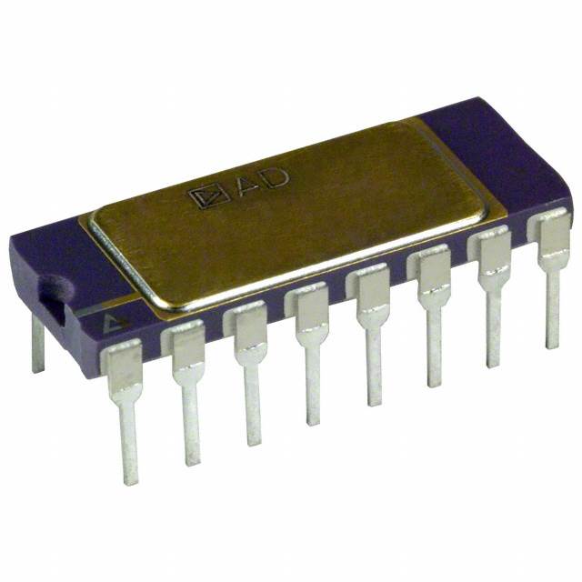
| 描述 | IC OPAMP GP 2.2MHZ 8SOIC运算放大器 - 运放 Low Pwr Programmable |
| 产品分类 | Linear - Amplifiers - Instrumentation, OP Amps, Buffer Amps集成电路 - IC |
| 品牌 | Texas Instruments |
| 产品手册 | |
| 产品图片 |
|
| rohs | 符合RoHS无铅 / 符合限制有害物质指令(RoHS)规范要求 |
| 产品系列 | 放大器 IC,运算放大器 - 运放,Texas Instruments TLC271ACDLinCMOS™ |
| 数据手册 | |
| 产品型号 | TLC271ACD |
| 产品目录页面 | |
| 产品种类 | 运算放大器 - 运放 |
| 供应商器件封装 | 8-SOIC |
| 共模抑制比—最小值 | 65 dB |
| 关闭 | No Shutdown |
| 其它名称 | 296-7338-5 |
| 包装 | 管件 |
| 单位重量 | 72.600 mg |
| 单电源电压 | 3 V to 16 V |
| 压摆率 | 5.3 V/µs |
| 商标 | Texas Instruments |
| 增益带宽生成 | 1.7 MHz |
| 增益带宽积 | 2.2MHz |
| 安装类型 | 表面贴装 |
| 安装风格 | SMD/SMT |
| 封装 | Tube |
| 封装/外壳 | 8-SOIC(0.154",3.90mm 宽) |
| 封装/箱体 | SOIC-8 |
| 工作温度 | 0°C ~ 70°C |
| 工作电源电压 | 3 V to 16 V |
| 工厂包装数量 | 75 |
| 技术 | LinCMOS |
| 放大器类型 | 通用 |
| 最大工作温度 | + 70 C |
| 最小工作温度 | 0 C |
| 标准包装 | 75 |
| 电压-电源,单/双 (±) | 3 V ~ 16 V, ±1.5 V ~ 8 V |
| 电压-输入失调 | 900µV |
| 电流-电源 | 950µA |
| 电流-输入偏置 | 0.7pA |
| 电流-输出/通道 | 30mA |
| 电源电流 | 675 uA |
| 电路数 | 1 |
| 系列 | TLC271A |
| 转换速度 | 3.6 V/us |
| 输入偏压电流—最大 | 60 pA |
| 输入参考电压噪声 | 25 nV |
| 输入补偿电压 | 0.9 mV |
| 输出类型 | - |
| 通道数量 | 1 Channel |


- 商务部:美国ITC正式对集成电路等产品启动337调查
- 曝三星4nm工艺存在良率问题 高通将骁龙8 Gen1或转产台积电
- 太阳诱电将投资9.5亿元在常州建新厂生产MLCC 预计2023年完工
- 英特尔发布欧洲新工厂建设计划 深化IDM 2.0 战略
- 台积电先进制程称霸业界 有大客户加持明年业绩稳了
- 达到5530亿美元!SIA预计今年全球半导体销售额将创下新高
- 英特尔拟将自动驾驶子公司Mobileye上市 估值或超500亿美元
- 三星加码芯片和SET,合并消费电子和移动部门,撤换高东真等 CEO
- 三星电子宣布重大人事变动 还合并消费电子和移动部门
- 海关总署:前11个月进口集成电路产品价值2.52万亿元 增长14.8%


PDF Datasheet 数据手册内容提取
TLC271, TLC271A, TLC271B LinCMOS PROGRAMMABLE LOW-POWER OPERATIONAL AMPLIFIERS SLOS090D – NOVEMBER 1987 – REVISED MARCH 2001 (cid:0) Input Offset Voltage Drift...Typically D, JG, OR P PACKAGE 0.1 µV/Month, Including the First 30 Days (TOP VIEW) (cid:0) Wide Range of Supply Voltages Over OFFSET N1 1 8 BIAS SELECT Specified Temperature Range: 0°C to 70°C...3 V to 16 V IN– 2 7 VDD –40°C to 85°C...4 V to 16 V IN+ 3 6 OUT –55°C to 125°C...5 V to 16 V GND 4 5 OFFSET N2 (cid:0) Single-Supply Operation FK PACKAGE (cid:0) Common-Mode Input Voltage Range (TOP VIEW) Extends Below the Negative Rail (C-Suffix T C 1 and I-Suffix Types) N E (cid:0) T EL Low Noise...25 nV/√Hz Typically at E S f = 1 kHz (High-Bias Mode) FS S C F CA C (cid:0) N O NBI N Output Voltage Range Includes Negative Rail 3 2 1 20 19 (cid:0) High Input Impedance...1012 Ω Typ NC 4 18 NC (cid:0) IN– 5 17 VDD ESD-Protection Circuitry NC 6 16 NC (cid:0) Small-Outline Package Option Also IN+ 7 15 OUT Available in Tape and Reel NC 8 14 NC (cid:0) 9 10 11 12 13 Designed-In Latch-Up Immunity C D C2 C description N N NN N G T E S The TLC271 operational amplifier combines a F F wide range of input offset voltage grades with low O offset voltage drift and high input impedance. In NC – No internal connection addition, the TLC271 offers a bias-select mode that allows the user to select the best combination of power dissipation and ac performance for a particular application. These devices use Texas Instruments silicon-gate LinCMOS technology, which provides offset voltage stability far exceeding the stability available with conventional metal-gate processes. AVAILABLE OPTIONS PACKAGE VVIIOOmmaaxx TA AT 25°C SMALL OUTLINE CHIP CARRIER CERAMIC DIP PLASTIC DIP (D) (FK) (JG) (P) 22 mmVV TTLLCC227711BBCCDD TTLLCC227711BBCCPP 0°C to 70°C 5 mV TLC271ACD — — TLC271ACP 10 mV TLC271CD TLC271CP 22 mmVV TTLLCC227711BBIIDD TTLLCC227711BBIIPP –40°C to 85°C 5 mV TLC271AID — — TLC271AIP 10 mV TLC271ID TLC271IP –55°C to 125°C 10 mV TLC271MD TLC271MFK TLC271MJG TLC271MP The D package is available taped and reeled. Add R suffix to the device type (e.g., TLC271BCDR). Please be aware that an important notice concerning availability, standard warranty, and use in critical applications of TexasInstruments semiconductor products and disclaimers thereto appears at the end of this data sheet. LinCMOS is a trademark of Texas Instruments. PRODUCTION DATA information is current as of publication date. Copyright 2001, Texas Instruments Incorporated Products conform to specifications per the terms of Texas Instruments standard warranty. Production processing does not necessarily include testing of all parameters. POST OFFICE BOX 655303 • DALLAS, TEXAS 75265 1
TLC271, TLC271A, TLC271B LinCMOS PROGRAMMABLE LOW-POWER OPERATIONAL AMPLIFIERS SLOS090D – NOVEMBER 1987 – REVISED MARCH 2001 DEVICE FEATURES BIAS-SELECT MODE PPAARRAAMMEETTEERR†† UUNNIITT HIGH MEDIUM LOW PD 3375 525 50 µW SR 3.6 0.4 0.03 V/µs Vn 25 32 68 nV/√Hz B1 1.7 0.5 0.09 MHz AVD 23 170 480 V/mV †Typical at VDD = 5 V, TA = 25°C description (continued) Using the bias-select option, these cost-effective devices can be programmed to span a wide range of applications that previously required BiFET, NFET, or bipolar technology. Three offset voltage grades are available (C-suffix and I-suffix types), ranging from the low-cost TLC271 (10 mV) to the TLC271B (2 mV) low-offset version. The extremely high input impedance and low bias currents, in conjunction with good common-mode rejection and supply voltage rejection, make these devices a good choice for new state-of-the-art designs as well as for upgrading existing designs. In general, many features associated with bipolar technology are available in LinCMOS operational amplifiers, without the power penalties of bipolar technology. General applications such as transducer interfacing, analog calculations, amplifier blocks, active filters, and signal buffering are all easily designed with the TLC271. The devices also exhibit low-voltage single-supply operation, making them ideally suited for remote and inaccessible battery-powered applications. The common-mode input voltage range includes the negative rail. A wide range of packaging options is available, including small-outline and chip-carrier versions for high-density system applications. The device inputs and output are designed to withstand –100-mA surge currents without sustaining latch-up. The TLC271 incorporates internal ESD-protection circuits that prevent functional failures at voltages up to 2000 V as tested under MIL-STD-883C, Method 3015.2; however, care should be exercised in handling these devices as exposure to ESD may result in the degradation of the device parametric performance. The C-suffix devices are characterized for operation from 0°C to 70°C. The I-suffix devices are characterized for operation from –40°C to 85°C. The M-suffix devices are characterized for operation over the full military temperature range of –55°C to 125°C. bias-select feature The TLC271 offers a bias-select feature that allows the user to select any one of three bias levels depending on the level of performance desired. The tradeoffs between bias levels involve ac performance and power dissipation (see Table 1). Table 1. Effect of Bias Selection on Performance MODE TTYYPPIICCAALL PPAARRAAMMEETTEERR VVAALLUUEESS TTAA == 2255°CC,, VVDDDD == 55 VV HIGH BIAS MEDIUM BIAS LOW BIAS UNIT RL = 10 kΩ RL = 100 kΩ RL = 1 MΩ PD Power dissipation 3.4 0.5 0.05 mW SR Slew rate 3.6 0.4 0.03 V/µs Vn Equivalent input noise voltage at f = 1 kHz 25 32 68 nV/√Hz B1 Unity-gain bandwidth 1.7 0.5 0.09 MHz φm Phase margin 46° 40° 34° AVD Large-signal differential voltage amplification 23 170 480 V/mV 2 POST OFFICE BOX 655303 • DALLAS, TEXAS 75265
TLC271, TLC271A, TLC271B LinCMOS PROGRAMMABLE LOW-POWER OPERATIONAL AMPLIFIERS SLOS090D – NOVEMBER 1987 – REVISED MARCH 2001 bias selection Bias selection is achieved by connecting the bias select pin to one of three voltage levels (see Figure 1). For medium-bias applications, it is recommended that the bias select pin be connected to the midpoint between the supply rails. This procedure is simple in split-supply applications, since this point is ground. In single-supply applications, the medium-bias mode necessitates using a voltage divider as indicated in Figure 1. The use of large-value resistors in the voltage divider reduces the current drain of the divider from the supply line. However, large-value resistors used in conjunction with a large-value capacitor require significant time to charge up to the supply midpoint after the supply is switched on. A voltage other than the midpoint can be used if it is within the voltages specified in Figure 1. VDD BIAS-SELECT VOLTAGE Low 1 MΩ BIAS MODE (single supply) To the Bias Medium Select Pin Low VDD High Medium 1 V to VDD – 1 V 1 MΩ High GND 0.01 µF Figure 1. Bias Selection for Single-Supply Applications high-bias mode In the high-bias mode, the TLC271 series features low offset voltage drift, high input impedance, and low noise. Speed in this mode approaches that of BiFET devices but at only a fraction of the power dissipation. Unity-gain bandwidth is typically greater than 1 MHz. medium-bias mode The TLC271 in the medium-bias mode features low offset voltage drift, high input impedance, and low noise. Speed in this mode is similar to general-purpose bipolar devices but power dissipation is only a fraction of that consumed by bipolar devices. POST OFFICE BOX 655303 • DALLAS, TEXAS 75265 3
TLC271, TLC271A, TLC271B LinCMOS PROGRAMMABLE LOW-POWER OPERATIONAL AMPLIFIERS SLOS090D – NOVEMBER 1987 – REVISED MARCH 2001 low-bias mode In the low-bias mode, the TLC271 features low offset voltage drift, high input impedance, extremely low power consumption, and high differential voltage gain. ORDER OF CONTENTS TOPIC BIAS MODE schematic all absolute maximum ratings all recommended operating conditions all electrical characteristics high operating characteristics (Figures 2–33) typical characteristics electrical characteristics medium operating characteristics (Figures 34–65) typical characteristics electrical characteristics low operating characteristics (Figures 66–97) typical characteristics parameter measurement information all application information all equivalent schematic VDD P3 P12 P9A R6 P4 P5 P9B P11 P1 P2 R2 IN – R1 P10 N5 N11 IN + R5 C1 P6A P6B P7B P7A P8 N12 N3 N9 N6 N7 N1 N2 N4 R3 D1 D2 R7 N13 R4 N10 OFFSET OFFSET OUT GND BIAS N1 N2 SELECT 4 POST OFFICE BOX 655303 • DALLAS, TEXAS 75265
TLC271, TLC271A, TLC271B LinCMOS PROGRAMMABLE LOW-POWER OPERATIONAL AMPLIFIERS SLOS090D – NOVEMBER 1987 – REVISED MARCH 2001 absolute maximum ratings over operating free-air temperature (unless otherwise noted)† Supply voltage, V (see Note 1) . . . . . . . . . . . . . . . . . . . . . . . . . . . . . . . . . . . . . . . . . . . . . . . . . . . . . . . . . . . . 18 V DD Differential input voltage, V (see Note 2) . . . . . . . . . . . . . . . . . . . . . . . . . . . . . . . . . . . . . . . . . . . . . . . . . . . ±V ID DD Input voltage range, V (any input) . . . . . . . . . . . . . . . . . . . . . . . . . . . . . . . . . . . . . . . . . . . . . . . . . . . –0.3 V to V I DD Input current, I . . . . . . . . . . . . . . . . . . . . . . . . . . . . . . . . . . . . . . . . . . . . . . . . . . . . . . . . . . . . . . . . . . . . . . . . . . ±5 mA I Output current, I . . . . . . . . . . . . . . . . . . . . . . . . . . . . . . . . . . . . . . . . . . . . . . . . . . . . . . . . . . . . . . . . . . . . . . . ±30 mA O Duration of short-circuit current at (or below) 25°C (see Note 3) . . . . . . . . . . . . . . . . . . . . . . . . . . . . . . Unlimited Continuous total dissipation . . . . . . . . . . . . . . . . . . . . . . . . . . . . . . . . . . . . . . . . . . . See Dissipation Rating Table Operating free-air temperature, T : C suffix . . . . . . . . . . . . . . . . . . . . . . . . . . . . . . . . . . . . . . . . . . . . 0°C to 70°C A I suffix . . . . . . . . . . . . . . . . . . . . . . . . . . . . . . . . . . . . . . . . . . . –40°C to 85°C M suffix . . . . . . . . . . . . . . . . . . . . . . . . . . . . . . . . . . . . . . . . . –55°C to 125°C Storage temperature range . . . . . . . . . . . . . . . . . . . . . . . . . . . . . . . . . . . . . . . . . . . . . . . . . . . . . . . . –65°C to 150°C Case temperature for 60 seconds: FK package . . . . . . . . . . . . . . . . . . . . . . . . . . . . . . . . . . . . . . . . . . . . . . 260°C Lead temperature 1,6 mm (1/16 inch) from case for 10 seconds: D or P package . . . . . . . . . . . . . . . . . 260°C Lead temperature 1,6 mm (1/16 inch) from case for 60 seconds: JG package . . . . . . . . . . . . . . . . . . . . 300°C †Stresses beyond those listed under “absolute maximum ratings” may cause permanent damage to the device. These are stress ratings only, and functional operation of the device at these or any other conditions beyond those indicated under “recommended operating conditions” is not implied. Exposure to absolute-maximum-rated conditions for extended periods may affect device reliability. NOTES: 1. All voltage values, except differential voltages, are with respect to network ground. 2. Differential voltages are at IN+ with respect to IN–. 3. The output may be shorted to either supply. Temperature and/or supply voltages must be limited to ensure that the maximum dissipation rating is not exceeded (see application section). DISSIPATION RATING TABLE TA ≤ 25°C DERATING FACTOR TA = 70°C TA = 85°C TA = 125°C PACKAGE POWER RATING ABOVE TA = 25°C POWER RATING POWER RATING POWER RATING D 725 mW 5.8 mW/°C 464 mW 377 mW 145 mW FK 1375 mW 11.0 mW/°C 880 mW 715 mW 275 mW JG 1050 mW 8.4 mW/°C 672 mW 546 mW 210 mW P 1000 mW 8.0 mW/°C 640 mW 520 mW 200 mW recommended operating conditions C SUFFIX I SUFFIX M SUFFIX UUNNIITT MIN MAX MIN MAX MIN MAX Supply voltage, VDD 3 16 4 16 5 16 V VDD = 5 V –0.2 3.5 –0.2 3.5 0 3.5 CCoommmmoonn-mmooddee iinnppuutt vvoollttaaggee, VVIICC VV VDD = 10 V –0.2 8.5 –0.2 8.5 0 8.5 Operating free-air temperature, TA 0 70 –40 85 –55 125 °C POST OFFICE BOX 655303 • DALLAS, TEXAS 75265 5
TLC271, TLC271A, TLC271B LinCMOS PROGRAMMABLE LOW-POWER OPERATIONAL AMPLIFIERS SLOS090D – NOVEMBER 1987 – REVISED MARCH 2001 HIGH-BIAS MODE electrical characteristics at specified free-air temperature (unless otherwise noted) TLC271C, TLC271AC, TLC271BC TTEESSTT PARAMETER CCOONNDDIITTIIOONNSS TAA†† VDD = 5 V VDD = 10 V UNIT MIN TYP MAX MIN TYP MAX 25°C 1.1 10 1.1 10 TTLLCC227711CC Full range 12 12 VVOO == 11.44 VV, VVIIOO IInnppuutt ooffffsseett vvoollttaaggee TTLLCC227711AACC VRIISCC = = 5 00 V Ω,,, Fu2ll5 r°aCnge 0.9 6.55 0.9 6.55 mmVV RRL = 1100 kkΩΩ 25°C 0.34 2 0.39 2 TTLLCC227711BBCC Full range 3 3 Average temperature coefficient 25°C to αVIO of input offset voltage 70°C 1.8 2 µV/°C IIIIOO IInnppuutt ooffffsseett ccuurrrreenntt ((sseeee NNoottee 44)) VOO = VDDDD/2,, 25°C 0.1 60 0.1 60 ppAA VIC = VDD/2 70°C 7 300 7 300 IIIIBB IInnppuutt bbiiaass ccuurrrreenntt ((sseeee NNoottee 44)) VOO = VDDDD/2,, 25°C 0.6 60 0.7 60 ppAA VIC = VDD/2 70°C 40 600 50 600 –0.2 –0.3 –0.2 –0.3 25°C to to to to V 4 4.2 9 9.2 CCoommmmoonn-mmooddee iinnppuutt vvoollttaaggee VICR –0.2 –0.2 range (see Note 5) Full range to to V 3.5 8.5 25°C 3.2 3.8 8 8.5 VOH High-level output voltage VRRVILLD == = 11 110000 kk00ΩΩ mVV, 0°C 3 3.8 7.8 8.5 V 70°C 3 3.8 7.8 8.4 25°C 0 50 0 50 VOL Low-level output voltage VVID = –110000 mVV, 0°C 0 50 0 50 mV IIOOLL == 00 70°C 0 50 0 50 25°C 5 23 10 36 AVD LLarge-siignall ddiifffferenttiiall RRL = 1100 kkΩΩ, 0°C 4 27 7.5 42 V/mV vvoollttaaggee aammplliiffiiccaattiioonn SSeeee NNoottee 66 70°C 4 20 7.5 32 25°C 65 80 65 85 CMRR Common-mode rejection ratio VIC = VICRmin 0°C 60 84 60 88 dB 70°C 60 85 60 88 25°C 65 95 65 95 kSVR SS((∆∆uVVpDDpDDlly-//v∆∆oVVllttIIaOOg))e rejjecttiion rattiio VVVVDOOD == =11 .5544 VVVV tto 1100 VV 0°C 60 94 60 94 dB 70°C 60 96 60 96 II(SEL) Input current (BIAS SELECT) VI(SEL) = 0 25°C –1.4 –1.9 µA VVOO = VVDDDD//22,, 25°C 675 1600 950 2000 IDD Supply current VIC = VDD/2, 0°C 775 1800 1125 2200 µA NNo lloadd 70°C 575 1300 750 1700 †Full range is 0°C to 70°C. NOTES: 4. The typical values of input bias current and input offset current below 5 pA were determined mathematically. 5. This range also applies to each input individually. 6. At VDD = 5 V, VO = 0.25 V to 2 V; at VDD = 10 V, VO = 1 V to 6 V. 6 POST OFFICE BOX 655303 • DALLAS, TEXAS 75265
TLC271, TLC271A, TLC271B LinCMOS PROGRAMMABLE LOW-POWER OPERATIONAL AMPLIFIERS SLOS090D – NOVEMBER 1987 – REVISED MARCH 2001 HIGH-BIAS MODE electrical characteristics at specified free-air temperature (unless otherwise noted) TLC271I, TLC271AI, TLC271BI TTEESSTT PARAMETER CCOONNDDIITTIIOONNSS TAA†† VDD = 5 V VDD = 10 V UNIT MIN TYP MAX MIN TYP MAX 25°C 1.1 10 1.1 10 TTLLCC227711II Full range 13 13 VVOO == 11.44 VV, VVIIOO IInnppuutt ooffffsseett vvoollttaaggee TTLLCC227711AAII VRIISCC = = 5 00 V Ω,,, Ful2l r5a°nCge 0.9 57 0.9 57 mmVV RRL = 1100 kkΩΩ 25°C 0.34 2 0.39 2 TTLLCC227711BBII Full range 3.5 3.5 Average temperature coefficient 25°C to αVIO of input offset voltage 85°C 1.8 2 µV/°C IIIIOO IInnppuutt ooffffsseett ccuurrrreenntt ((sseeee NNoottee 44)) VOO = VDDDD/2,, 25°C 0.1 60 0.1 60 ppAA VIC = VDD/2 85°C 24 1000 26 1000 IIIIBB IInnppuutt bbiiaass ccuurrrreenntt ((sseeee NNoottee 44)) VOO = VDDDD/2,, 25°C 0.6 60 0.7 60 ppAA VIC = VDD/2 85°C 200 2000 220 2000 –0.2 –0.3 –0.2 –0.3 25°C to to to to V Common-mode input 4 4.2 9 9.2 VVIICCRR voltage range (see Note 5) –0.2 –0.2 Full range to to V 3.5 8.5 25°C 3.2 3.8 8 8.5 VOH High-level output voltage VVRRILLD == = 11 110000 kk00ΩΩ mVV, –40°C 3 3.8 7.8 8.5 V 85°C 3 3.8 7.8 8.5 25°C 0 50 0 50 VOL Low-level output voltage VVID = –110000 mVV, –40°C 0 50 0 50 mV IIOOLL == 00 85°C 0 50 0 50 25°C 5 23 10 36 AVD LLarge-siignall ddiifffferenttiiall RRL = 1100 kkΩΩ, –40°C 3.5 32 7 46 V/mV vvoollttaaggee aammplliiffiiccaattiioonn SSeeee NNoottee 66 85°C 3.5 19 7 31 25°C 65 80 65 85 CMRR Common-mode rejection ratio VIC = VICRmin –40°C 60 81 60 87 dB 85°C 60 86 60 88 25°C 65 95 65 95 kSVR SS((∆∆uVVpDDpDDlly-//v∆∆oVVllttIIaOOg))e rejjecttiion rattiio VVVVDOOD == =11 .5544 VVVV tto 1100 VV –40°C 60 92 60 92 dB 85°C 60 96 60 96 II(SEL) Input current (BIAS SELECT) VI(SEL) = 0 25°C –1.4 –1.9 µA VVOO = VVDDDD//22,, 25°C 675 1600 950 2000 IDD Supply current VIC = VDD/2, –40°C 950 2200 1375 2500 µA NNo lloadd 85°C 525 1200 725 1600 †Full range is –40°C to 85°C. NOTES: 4. The typical values of input bias current and input offset current below 5 pA were determined mathematically. 5. This range also applies to each input individually. 6. At VDD = 5 V, VO = 0.25 V to 2 V; at VDD = 10 V, VO = 1 V to 6 V. POST OFFICE BOX 655303 • DALLAS, TEXAS 75265 7
TLC271, TLC271A, TLC271B LinCMOS PROGRAMMABLE LOW-POWER OPERATIONAL AMPLIFIERS SLOS090D – NOVEMBER 1987 – REVISED MARCH 2001 HIGH-BIAS MODE electrical characteristics at specified free-air temperature (unless otherwise noted) TLC271M TTEESSTT PARAMETER CCOONNDDIITTIIOONNSS TAA†† VDD = 5 V VDD = 10 V UNIT MIN TYP MAX MIN TYP MAX VVOO == 11..44 VV,, 2255°°CC 11.11 1100 11.11 1100 VVIIOO IInnppuutt ooffffsseett vvoollttaaggee RVIISSCC = = 5 00 V Ω,,, mmVV RL = 10 kΩ FFuullll rraannggee 1122 1122 Average temperature coefficient 25°C to αVIO of input offset voltage 125°C 2.1 2.2 µV/°C IIIIOO IInnppuutt ooffffsseett ccuurrrreenntt ((sseeee NNoottee 44)) VOO = VDDDD/2,, 25°C 0.1 60 0.1 60 pA VIC = VDD/2 125°C 1.4 15 1.8 15 nA IIIIBB IInnppuutt bbiiaass ccuurrrreenntt ((sseeee NNoottee 44)) VOO = VDDDD/2,, 25°C 0.6 60 0.7 60 pA VIC = VDD/2 125°C 9 35 10 35 nA 0 –0.3 0 –0.3 25°C to to to to V Common-mode input voltagge 4 4.2 9 9.2 VVIICCRR range (see Note 5) 0 0 Full range to to V 3.5 8.5 25°C 3.2 3.8 8 8.5 VOH High-level output voltage VRRVILLD == = 11 110000 kk00ΩΩ mVV, –55°C 3 3.8 7.8 8.5 V 125°C 3 3.8 7.8 8.4 25°C 0 50 0 50 VOL Low-level output voltage VVID = –110000 mVV, –55°C 0 50 0 50 mV IIOOLL == 00 125°C 0 50 0 50 25°C 5 23 10 36 AVD LLarge-siignall ddiifffferenttiiall RRL = 1100 kkΩΩ, –55°C 3.5 35 7 50 V/mV vvoollttaaggee aammplliiffiiccaattiioonn SSeeee NNoottee 66 125°C 3.5 16 7 27 25°C 65 80 65 85 CMRR Common-mode rejection ratio VIC = VICRmin –55°C 60 81 60 87 dB 125°C 60 84 60 86 25°C 65 95 65 95 kSVR SS((∆∆uVVpDDpDDlly-//v∆∆oVVllttIIaOOg))e rejjecttiion rattiio VVVVDOOD == =11 .5544 VVVV tto 1100 VV –55°C 60 90 60 90 dB 125°C 60 97 60 97 II(SEL) Input current (BIAS SELECT) VI(SEL) = 0 25°C –1.4 –1.9 µA VVOO = VVDDDD//22,, 25°C 675 1600 950 2000 IDD Supply current VIC = VDD/2, –55°C 1000 2500 1475 3000 µA NNo lloadd 125°C 475 1100 625 1400 †Full range is –55°C to 125°C. NOTES: 4. The typical values of input bias current and input offset current below 5 pA were determined mathematically. 5. This range also applies to each input individually. 6. At VDD = 5 V, VO = 0.25 V to 2 V; at VDD = 10 V, VO = 1 V to 6 V. 8 POST OFFICE BOX 655303 • DALLAS, TEXAS 75265
TLC271, TLC271A, TLC271B LinCMOS PROGRAMMABLE LOW-POWER OPERATIONAL AMPLIFIERS SLOS090D – NOVEMBER 1987 – REVISED MARCH 2001 HIGH-BIAS MODE operating characteristics at specified free-air temperature, V = 5 V DD TLC271C, TLC271AC, PARAMETER TEST CONDITIONS TAA TLC271BC UNIT MIN TYP MAX 25°C 3.6 VI((PP)) = 1 V 0°C 4 RL = 10 kΩ, 70°C 3 SSRR SSlleeww rraattee aatt uunniittyy ggaaiinn CCLL = 2200 ppFF, 25°C 2.9 VV//µµss SSeeee FFiigguurree 9988 VI((PP)) = 2.5 V 0°C 3.1 70°C 2.5 VVn EEqquuiivvaalleenntt iinnppuutt nnooiissee vvoollttaaggee f = 1 kHz,, RSS = 20 Ω,, 2255°°CC 2255 nnVV//√√HHzz See Figure 99 25°C 320 BOM Maximum output-swing bandwidth VRRVOLL === 11VV00O kkHΩΩ ,, CCSSeeLee = FF 22iigg00uu prreeFF, 9988 0°C 340 kHz 70°C 260 25°C 1.7 B1 Unity-gain bandwidth VVI = 1100 mVV, CCL = 2200 pFF, 0°C 2 MHz SSeeee FFiigguurree 110000 70°C 1.3 25°C 46° φm Phase margin VVCCILL = == 11 220000 mm pVVFF,,, ffSS =ee eeBB FF1,iigguurree 110000 0°C 47° 70°C 44° operating characteristics at specified free-air temperature, V = 10 V DD TLC271C, TLC271AC, PARAMETER TEST CONDITIONS TAA TLC271BC UNIT MIN TYP MAX 25°C 5.3 VI((PP)) = 1 V 0°C 5.9 RL = 10 kΩ, 70°C 4.3 SSRR SSlleeww rraattee aatt uunniittyy ggaaiinn CCLL = 2200 ppFF, 25°C 4.6 VV//µµss SSeeee FFiigguurree 9988 VI((PP)) = 5.5 V 0°C 5.1 70°C 3.8 VVn EEqquuiivvaalleenntt iinnppuutt nnooiissee vvoollttaaggee f = 1 kHz,, RSS = 20 Ω,, 2255°°CC 2255 nnVV//√√HHzz See Figure 99 25°C 200 BOM Maximum output-swing bandwidth VRRVOLL === 11VV00O kkHΩΩ,, CCSSeeLee = FF 22iigg00uu prreeFF, 9988 0°C 220 kHz 70°C 140 25°C 2.2 B1 Unity-gain bandwidth VVI = 1100 mVV, CCL = 2200 pFF, 0°C 2.5 MHz SSeeee FFiigguurree 110000 70°C 1.8 25°C 49° φm Phase margin ffCC =LL BB==1 22,00 pFF,, VVSSIee =ee FF1100iigg uummrrVVee, 110000 0°C 50° 70°C 46° POST OFFICE BOX 655303 • DALLAS, TEXAS 75265 9
TLC271, TLC271A, TLC271B LinCMOS PROGRAMMABLE LOW-POWER OPERATIONAL AMPLIFIERS SLOS090D – NOVEMBER 1987 – REVISED MARCH 2001 HIGH-BIAS MODE operating characteristics at specified free-air temperature, V = 5 V DD TLC271I, TLC271AI, PARAMETER TEST CONDITIONS TAA TLC271BI UNIT MIN TYP MAX 25°C 3.6 VI((PP)) = 1 V –40°C 4.5 RL = 10 kΩ, 85°C 2.8 SSRR SSlleeww rraattee aatt uunniittyy ggaaiinn CCLL == 2200 ppFF, VV//µµss 25°C 2.9 SSeeee FFiigguurree 9988 VI((PP)) = 2.5 V –40°C 3.5 85°C 2.3 VVn EEqquuiivvaalleenntt iinnppuutt nnooiissee vvoollttaaggee f = 1 kHz,, RSS = 20 Ω,, 2255°°CC 2255 nnVV//√√HHz See Figure 99 25°C 320 BOM Maximum output-swing bandwidth VVRROLL === 11VV00O kkHΩΩ,, CCSSeeLee = FF 22iigg00uu prreeFF, 9988 –40°C 380 kHz 85°C 250 25°C 1.7 B1 Unity-gain bandwidth VVI = 1100 mVV, CCL = 2200 pFF, –40°C 2.6 MHz SSeeee FFiigguurree 110000 85°C 1.2 25°C 46° φm Phase margin VVCCILL = == 11 220000 mm pVVFF,, ffSS =ee eeBB FF1,iigguurree 110000 –40°C 49° 85°C 43° operating characteristics at specified free-air temperature, V = 10 V DD TLC271I, TLC271AI, PARAMETER TEST CONDITIONS TAA TLC271BI UNIT MIN TYP MAX 25°C 5.3 VI((PP)) = 1 V –40°C 6.8 RL = 10 kΩ, 85°C 4 SSRR SSlleeww rraattee aatt uunniittyy ggaaiinn CCLL == 2200 ppFF, VV//µµss 25°C 4.6 SSeeee FFiigguurree 9988 VI((PP)) = 5.5 V –40°C 5.8 85°C 3.5 VVn EEqquuiivvaalleenntt iinnppuutt nnooiissee vvoollttaaggee f = 1 kHz,, RSS = 20 Ω,, 2255°°CC 2255 nnVV//√√HHzz See Figure 99 25°C 200 BOM Maximum output-swing bandwidth VVRROLL === 11VV00O kkHΩΩ,, CCSSeeLee = FF 22iigg00uu prreeFF, 9988 –40°C 260 kHz 85°C 130 25°C 2.2 B1 Unity-gain bandwidth VVI = 1100 mVV, CCL = 2200 pFF, –40°C 3.1 MHz SSeeee FFiigguurree 110000 85°C 1.7 25°C 49° φm Phase margin VVCCILL = == 11 220000 mm pVVFF,, ffSS=ee BBee 1FF,iigguurree 110000 –40°C 52° 85°C 46° 10 POST OFFICE BOX 655303 • DALLAS, TEXAS 75265
TLC271, TLC271A, TLC271B LinCMOS PROGRAMMABLE LOW-POWER OPERATIONAL AMPLIFIERS SLOS090D – NOVEMBER 1987 – REVISED MARCH 2001 HIGH-BIAS MODE operating characteristics at specified free-air temperature, V = 5 V DD TLC271M PPAARRAAMMEETTEERR TTEESSTT CCOONNDDIITTIIOONNSS TTAA UUNNIITT MIN TYP MAX 25°C 3.6 VI((PP)) = 1 V –55°C 4.7 RL = 10 kΩ, 125°C 2.3 SSRR SSlleeww rraattee aatt uunniittyy ggaaiinn CCLL = 2200 ppFF, 25°C 2.9 VV//µµss SSeeee FFiigguurree 9988 VI((PP)) = 2.5 V –55°C 3.7 125°C 2 VVn EEqquuiivvaalleenntt iinnppuutt nnooiissee vvoollttaaggee f = 1 kHz,, RSS = 20 Ω,, 2255°°CC 2255 nnVV//√√HHz See Figure 99 25°C 320 BOM Maximum output-swing bandwidth VVRROLL === 11VV00O kkHΩΩ,, CCSSeeLee = FF 22iigg00uu prreeFF, 9988 –55°C 400 kHz 125°C 230 25°C 1.7 B1 Unity-gain bandwidth VVI = 1100 mVV, CCL = 2200 pFF, –55°C 2.9 MHz SSeeee FFiigguurree 110000 125°C 1.1 25°C 46° φm Phase margin VVCCILL = == 11 220000 mm pVVFF,,, ffSS =ee eeBB FF1,iigguurree 110000 –55°C 49° 125°C 41° operating characteristics at specified free-air temperature, V = 10 V DD TLC271M PPAARRAAMMEETTEERR TTEESSTT CCOONNDDIITTIIOONNSS TTAA UUNNIITT MIN TYP MAX 25°C 5.3 VI((PP)) = 1 V –55°C 7.1 RL = 10 kΩ, 125°C 3.1 SSRR SSlleeww rraattee aatt uunniittyy ggaaiinn CCLL = 2200 ppFF, 25°C 4.6 VV//µµss SSeeee FFiigguurree 9988 VI((PP)) = 5.5 V –55°C 6.1 125°C 2.7 VVn EEqquuiivvaalleenntt iinnppuutt nnooiissee vvoollttaaggee f = 1 kHz,, RSS = 20 Ω,, 2255°°CC 2255 nnVV//√√HHz See Figure 99 25°C 200 BOM Maximum output-swing bandwidth VVRROLL === 11VV00O kkHΩΩ,, CCSSeeLee = FF 22iigg00uu prreeFF, 9988 –55°C 280 kHz 125°C 110 25°C 2.2 B1 Unity-gain bandwidth VVI = 1100 mVV, CCL = 2200 pFF, –55°C 3.4 MHz SSeeee FFiigguurree 110000 125°C 1.6 25°C 49° φm Phase margin ffCC =LL BB==1 22,00 pFF,, VVSSIee =ee FF1100iigg uummrrVVee, 110000 –55°C 52° 125°C 44° POST OFFICE BOX 655303 • DALLAS, TEXAS 75265 11
TLC271, TLC271A, TLC271B LinCMOS PROGRAMMABLE LOW-POWER OPERATIONAL AMPLIFIERS SLOS090D – NOVEMBER 1987 – REVISED MARCH 2001 TYPICAL CHARACTERISTICS (HIGH-BIAS MODE) Table of Graphs FIGURE VIO Input offset voltage Distribution 2, 3 αVIO Temperature coefficient Distribution 4, 5 vvss HHiigghh-lleevveell oouuttpuutt ccuurrrreenntt 66,, 77 VOOHH Higgh-level output voltagge vs Supplyy voltagge 8 vs Free-air temperature 9 vvss CCoommmmoonn-mmooddee iinnpuutt vvoollttaaggee 1100,, 1111 vs Differential input voltagge 12 VVOOLL LLooww-lleevveell oouuttppuutt vvoollttaaggee vs Free-air temperature 13 vs Low-level output current 14, 15 vvss SSuuppllyy vvoollttaaggee 1166 AVVDD Largge-siggnal differential voltagge amplification vs Free-air temperature 17 vs Frequency 28, 29 IIB Input bias current vs Free-air temperature 18 IIO Input offset current vs Free-air temperature 18 VIC Common-mode input voltage vs Supply voltage 19 vs Supplyy voltagge 20 IIDDDD SSuuppppllyy ccuurrrreenntt vs Free-air temperature 21 vs Supplyy voltagge 22 SSRR SSlleeww rraattee vs Free-air temperature 23 Bias-select current vs Supply voltage 24 VO(PP) Maximum peak-to-peak output voltage vs Frequency 25 vs Free-air temperature 26 BB11 UUnniittyy-ggaaiinn bbaannddwwiiddtthh vs Supply voltage 27 AVD Large-signal differential voltage amplification vs Frequency 28, 29 vvss SSuuppllyy vvoollttaaggee 3300 φφmm Phase marggin vs Free-air temperature 31 vs Capacitive load 32 Vn Equivalent input noise voltage vs Frequency 33 Phase shift vs Frequency 28, 29 12 POST OFFICE BOX 655303 • DALLAS, TEXAS 75265
TLC271, TLC271A, TLC271B LinCMOS PROGRAMMABLE LOW-POWER OPERATIONAL AMPLIFIERS SLOS090D – NOVEMBER 1987 – REVISED MARCH 2001 TYPICAL CHARACTERISTICS (HIGH-BIAS MODE)† DISTRIBUTION OF TLC271 DISTRIBUTION OF TLC271 INPUT OFFSET VOLTAGE INPUT OFFSET VOLTAGE ÎÎÎÎÎÎÎÎÎÎÎÎÎ 60 60 ÎÎÎÎÎÎÎÎÎÎÎÎ ÎÎ753 ÎAmpÎlifieÎrs TÎesteÎd FrÎom Î6 WaÎfer ÎLotsÎÎ 753 Amplifiers Tested From 6 Wafer Lots VDD = 5 V VDD = 10 V 50 TA = 25°C 50 TA = 25°C P Package P Package % % s – 40 s – 40 nit nit U U e of 30 e of 30 g g a a nt nt e e c 20 c 20 er er P P 10 10 0 0 – 5 – 4 – 3 – 2 – 1 0 1 2 3 4 5 – 5 – 4 – 3 – 2 – 1 0 1 2 3 4 5 VIO – Input Offset Voltage – mV VIO – Input Offset Voltage – mV Figure 2 Figure 3 DISTRIBUTION OF TLC271 DISTRIBUTION OF TLC271 INPUT OFFSET VOLTAGE INPUT OFFSET VOLTAGE TEMPERATURE COEFFICIENT TEMPERATURE COEFFICIENT ÎÎÎÎÎÎÎÎÎÎÎÎ ÎÎÎÎÎÎÎÎÎÎÎÎ 60 60 Î32Î4 AmÎpliÎfiersÎ TesÎted ÎFromÎ 8 WÎafeÎr LoÎts Î ÎÎ324 ÎAmpÎlifieÎrs TÎesteÎd FrÎom 8Î WaÎfer lÎotsÎ VDD = 5 V VDD = 10 V 50 TA = 25°C to 125°C 50 TA = 25°C to 125°C P Package P Package % Outliers: % Outliers: s – 40 Î(1Î) 20.Î5 µVÎ/°CÎ s – 40ÎÎ(1) 2Î1.2 εV/°ÎC nit nit U U e of 30 e of 30 g g a a nt nt e e erc 20 erc 20 P P 10 10 0 0 – 10 – 8 – 6 – 4 – 2 0 2 4 6 8 10 – 10 – 8 – 6 – 4 – 2 0 2 4 6 8 10 αVIO – Temperature Coefficient – µV/°C αVIO – Temperature Coefficient – µV/°C Figure 4 Figure 5 †Data at high and low temperatures are applicable only within the rated operating free-air temperature ranges of the various devices. POST OFFICE BOX 655303 • DALLAS, TEXAS 75265 13
TLC271, TLC271A, TLC271B LinCMOS PROGRAMMABLE LOW-POWER OPERATIONAL AMPLIFIERS SLOS090D – NOVEMBER 1987 – REVISED MARCH 2001 TYPICAL CHARACTERISTICS (HIGH-BIAS MODE)† HIGH-LEVEL OUTPUT VOLTAGE HIGH-LEVEL OUTPUT VOLTAGE vs vs HIGH-LEVEL OUTPUT CURRENT HIGH-LEVEL OUTPUT CURRENT 5 16 VID = 100 mV VID = 100 mV e – V 4 TA = 25°C e – V 14 VDD = 16 V TA = 25°C ag ag 12 olt olt V V ut 3 VDD = 5 V ut 10 p p Out VDD = 4 V Out ÎÎÎÎÎ vel vel 8 ÎVÎDD Î= 10Î V Î Le 2 VDD = 3 V Le h- h- 6 g g ÁÁHiÁ ÁHiÁ – – 4 ÁÁOH OHÁ1 ÁOH OHÁ VV VV ÁÁÁ ÁÁ2 0 0 0 – 2 – 4 – 6 – 8 – 10 0 – 5 – 10 – 15 – 20 – 25 – 30 – 35 – 40 IOH – High-Level Output Current – mA IOH – High-Level Output Current – mA Figure 6 Figure 7 HIGH-LEVEL OUTPUT VOLTAGE HIGH-LEVEL OUTPUT VOLTAGE vs vs SUPPLY VOLTAGE FREE-AIR TEMPERATURE 16 VDD – 1.6 e – V 14 TRVAILD == = 21 1500° kC0Ω mV e – V – 1.7 VDD = 5 V IVOIDH == 1–050 m mAA ag 12 ag – 1.8 olt olt V V ut 10 ut – 1.9 p p ut ut el O 8 el O – 2 ev ev VDD = 10 V h-L 6 h-L – 2.1 g g Hi Hi Á– Á4 Á– Á– 2.2 H H H H ÁOOÁ ÁOOÁ VV VV 2 – 2.3 0 – 2.4 0 2 4 6 8 10 12 14 16 – 75 – 50 – 25 0 20 50 75 100 125 VDD – Supply Voltage – V TA – Free-Air Temperature – °C Figure 8 Figure 9 †Data at high and low temperatures are applicable only within the rated operating free-air temperature ranges of the various devices. 14 POST OFFICE BOX 655303 • DALLAS, TEXAS 75265
TLC271, TLC271A, TLC271B LinCMOS PROGRAMMABLE LOW-POWER OPERATIONAL AMPLIFIERS SLOS090D – NOVEMBER 1987 – REVISED MARCH 2001 TYPICAL CHARACTERISTICS (HIGH-BIAS MODE)† LOW-LEVEL OUTPUT VOLTAGE LOW-LEVEL OUTPUT VOLTAGE vs vs COMMON-MODE INPUT VOLTAGE COMMON-MODE INPUT VOLTAGE 700 500 VDD = 5 V VDD = 10 V – mV 650 TIOAL = = 2 55 °mCA – mV 450 ITOAL = = 2 55 °mCA e 600 e g g a a olt olt Output V 550500 ÎÎVÎÎID =ÎÎ –10ÎÎ0 mÎÎV ÎÎ Output V 400 VID = –100 mV w-Level 450 w-Level 350 VVIIDD == ––12 .V5 V o o ÁÁVOL – LVOLÁÁ430500 VID = –1 V ÁÁÁÁVOL – LVOLÁÁ300 300 250 0 1 2 3 4 0 1 2 3 4 5 6 7 8 9 10 VIC – Common-Mode Input Voltage – V VIC – Common-Mode Input Voltage – V Figure 10 Figure 11 LOW-LEVEL OUTPUT VOLTAGE LOW-LEVEL OUTPUT VOLTAGE vs vs DIFFERENTIAL INPUT VOLTAGE FREE-AIR TEMPERATURE 800 900 IOL = 5 mA IOL = 5 mA 700 VIC = VID/2 800 VID = –1 V mV TA = 25°C mV VIC = 0.5 V – – 700 e 600 e g g put Volta 500 ÎVDÎD = Î5 VÎ put Volta 560000 ÎVDÎD = Î5 VÎ ut 400 ÎÎÎÎ ut O O el el 400 ÎÎÎÎ Lev 300 Lev 300 ÎVÎDD =Î 10 ÎV w- VDD = 10 V w- o o L 200 L ÁL – LÁ ÁL – ÁL 200 OO OO ÁVVÁ100 ÁVÁV 100 0 0 0 – 1 – 2 – 3 – 4 – 5 – 6 – 7 – 8 – 9 – 10 – 75 – 50 – 25 0 25 50 75 100 125 VID – Differential Input Voltage – V TA – Free-Air Temperature – °C Figure 12 Figure 13 †Data at high and low temperatures are applicable only within the rated operating free-air temperature ranges of the various devices. POST OFFICE BOX 655303 • DALLAS, TEXAS 75265 15
TLC271, TLC271A, TLC271B LinCMOS PROGRAMMABLE LOW-POWER OPERATIONAL AMPLIFIERS SLOS090D – NOVEMBER 1987 – REVISED MARCH 2001 TYPICAL CHARACTERISTICS (HIGH-BIAS MODE)† LOW-LEVEL OUTPUT VOLTAGE LOW-LEVEL OUTPUT VOLTAGE vs vs LOW-LEVEL OUTPUT CURRENT LOW-LEVEL OUTPUT CURRENT 1 3 VID = –1 V VID = –1 V 0.9 VIC = 0.5 V VIC = 0.5 V mV TA = 25°C mV 2.5 TA = 25°C ge – 0.8 VDD = 5 V ge – VDD = 16 V ut Volta 00..67 ÎÎÎÎVÎÎDD Î= 4 VÎ ut Volta 2 VDD = 10 V Outp 0.5 ÎVÎDD =Î 3 VÎ Outp 1.5 Level 0.4 Level ow- 0.3 Áow-Á 1 L L ÁÁVOL – VOLÁÁ0.2 ÁÁVOL – VÁÁOL 0.5 0.1 0 0 0 1 2 3 4 5 6 7 8 0 5 10 15 20 25 30 IOL – Low-Level Output Current – mA IOL – Low-Level Output Current – mA Figure 14 Figure 15 LARGE-SIGNAL LARGE-SIGNAL DIFFERENTIAL VOLTAGE AMPLIFICATION DIFFERENTIAL VOLTAGE AMPLIFICATION vs vs SUPPLY VOLTAGE FREE-AIR TEMPERATURE 60 50 ÎRLÎ = 1Î0 kΩÎ TA = –55°C ÎRÎL =Î 10 kÎΩ Î ÎÎÎÎ ÎÎÎ 45 ÎÎÎÎÎ al V 50 ÎÎ0°CÎ al V 40 VDD = 10 V nal Differenti cation – V/m 40 ÎÎÎÎ2855°°ÎÎCC nal Differenti cation – V/m 3305 Sig plifi 30 125°C Sig plifi 25 e- m e- m arg e A arg e A 20 VDD = 5 V ÁÁÁÁVD – LVDVoltag 20 ÁÁVD – LVDÁÁVoltag 15 AA AA 10 ÁÁ 10 ÁÁ 5 0 0 0 2 4 6 8 10 12 14 16 – 75 – 50 – 25 0 25 50 75 100 125 VDD – Supply Voltage – V TA – Free-Air Temperature – °C Figure 16 Figure 17 †Data at high and low temperatures are applicable only within the rated operating free-air temperature ranges of the various devices. 16 POST OFFICE BOX 655303 • DALLAS, TEXAS 75265
TLC271, TLC271A, TLC271B LinCMOS PROGRAMMABLE LOW-POWER OPERATIONAL AMPLIFIERS SLOS090D – NOVEMBER 1987 – REVISED MARCH 2001 TYPICAL CHARACTERISTICS (HIGH-BIAS MODE)† INPUT BIAS CURRENT AND INPUT OFFSET COMMON-MODE INPUT VOLTAGE CURRENT (POSITIVE LIMIT) vs vs FREE-AIR TEMPERATURE SUPPLY VOLTAGE 10000 ÁÁÁÁ 16 ÁVVDICÁD = = 5 Á1 V0 VÁ V TA = 25°C See Note A – 14 ÁÁÁÁ e 1000 g O – Input Bias andOset Currents – nA 100 ÎÎIIBÎÎ ÎÎIIOÎÎ n-Mode Input Volta 11802 d IIIIOff 10 mo 6 IIB anIIBInput – Com 4 1 C VI 2 0.1 0 25 45 65 85 105 125 0 2 4 6 8 10 12 14 16 TA – Free-Air Temperature – °C VDD – Supply Voltage – V NOTE A: The typical values of input bias current and input offset current below 5 pA were determined mathematically. Figure 18 Figure 19 SUPPLY CURRENT SUPPLY CURRENT vs vs SUPPLY VOLTAGE FREE-AIR TEMPERATURE 2.5 2 ÎÎÎÎ ÎÎÎÎÎ VO = VDD/2 VO = VDD/2 No Load No Load ÎÎÎÎ ÎÎÎÎÎ 2 TA =–55°C A A 1.5 m m – – ent 1.5 ÎÎ0°CÎ ent urr urr VDD = 10 V y C 25°C y C 1 pl pl ÁÁ– SupÁ1 70°C Á– SupÁ ÁÁD DÁ ÁD ÁD VDD = 5 V DD 125°C DD 0.5 ÁÁIIÁ ÁIIÁ 0.5 0 0 0 2 4 6 8 10 12 14 16 – 75 – 50 – 25 0 25 50 75 100 125 VDD – Supply Voltage – V TA – Free-Air Temperature – °C Figure 20 Figure 21 †Data at high and low temperatures are applicable only within the rated operating free-air temperature ranges of the various devices. POST OFFICE BOX 655303 • DALLAS, TEXAS 75265 17
TLC271, TLC271A, TLC271B LinCMOS PROGRAMMABLE LOW-POWER OPERATIONAL AMPLIFIERS SLOS090D – NOVEMBER 1987 – REVISED MARCH 2001 TYPICAL CHARACTERISTICS (HIGH-BIAS MODE)† SLEW RATE SLEW RATE vs vs SUPPLY VOLTAGE FREE-AIR TEMPERATURE 8 8 AVVI(P =P 1) = 1 V ÎÎÎÎÎ RAVL == 110 kΩ 7 RL = 10 kΩ 7 ÎÎÎÎVDDÎÎ = 1ÎÎ0 V ÎÎ CL = 20 pF CL = 20 pF ÎÎVI(PÎP) =Î 5.5 ÎV See Figure 99 6 TA = 25°C 6 ss ss µV/ u See Figure 98 µV/ u VDD = 10 V – 5 – 5 ÎVÎI(PPÎ) = 1Î V e e at at R 4 R 4 w w e e Sl Sl – 3 – 3 R R S S 2 2 VDD = 5 V VI(PP) = 1 V ÎÎÎÎÎ 1 1 ÎÎÎÎVDDÎÎ = 5ÎÎ V ÎÎÎ VI(PP) = 2.5 V ÎÎÎÎÎÎ 0 0 0 2 4 6 8 10 12 14 16 –75 –50 –25 0 25 50 75 100 125 VDD – Supply Voltage – V TA – Free-Air Temperature – °C Figure 22 Figure 23 MAXIMUM PEAK-TO-PEAK OUTPUT BIAS-SELECT CURRENT VOLTAGE vs vs SUPPLY VOLTAGE FREQUENCY – 3 V 10 – 2.7 VTAI( S=E 2L5)° =C 0 age – 9 ÎÎVDÎÎD = ÎÎ10 VÎÎ – 2.4 Volt 8 ÎÎÎÎ ut TA = 125°C µuaA – 2.1 utp 7 ÎÎÎTAÎÎÎ = 25ÎÎΰC ÎÎÎ – O ÎTAÎ = 55ΰC Î rrent – 1.8 Peak 6 elect Cu –– 11..25 Peak-to- 54 ÎÎVDÎÎD = ÎÎ5 VÎÎ Bias-S –– 00..69 aximum 32 ÎÎRLÎÎ = 1ÎÎ0 kΩÎÎÎ M ÎSeÎe FigÎureÎ 98Î – – 0.3 P) 1 P 0 O( 0 V 0 2 4 6 8 10 12 14 16 10 100 1000 10000 VDD – Supply Voltage – V f – Frequency – kHz Figure 24 Figure 25 †Data at high and low temperatures are applicable only within the rated operating free-air temperature ranges of the various devices. 18 POST OFFICE BOX 655303 • DALLAS, TEXAS 75265
TLC271, TLC271A, TLC271B LinCMOS PROGRAMMABLE LOW-POWER OPERATIONAL AMPLIFIERS SLOS090D – NOVEMBER 1987 – REVISED MARCH 2001 TYPICAL CHARACTERISTICS (HIGH-BIAS MODE)† UNITY-GAIN BANDWIDTH UNITY-GAIN BANDWIDTH vs vs FREE-AIR TEMPERATURE SUPPLY VOLTAGE 3 2.5 VDD = 5 V VI = 10 mV VI = 10 mV CL = 20 pF CL = 20 pF TA = 25°C Hz See Figure 100 Hz See Figure 100 M M – 2.5 – h h dt dt 2 wi wi d d n n a a B 2 B n n ai ai G G y- y- nit nit 1.5 U U – 1.5 – 1 1 1 1 BB BB 1 1 – 75 – 50 – 25 0 25 50 75 100 125 0 2 4 6 8 10 12 14 16 TA – Free-Air Temperature – °C VDD – Supply Voltage – V Figure 26 Figure 27 LARGE-SIGNAL DIFFERENTIAL VOLTAGE AMPLIFICATION AND PHASE SHIFT vs FREQUENCY 107 VDD = 5 V 106 RL = 10 kΩ TA = 25°C al nti 105 0° e n nal Differ plificatio 104 AVD 30° Shift Sig Am 103 60° se Large- oltage 102 90° Pha – V Phase Shift ÁVD VDÁ 101 120° ÁAAÁ 1 150° 0.1 180° 10 100 1 k 10 k 100 k 1 M 10 M f – Frequency – Hz Figure 28 †Data at high and low temperatures are applicable only within the rated operating free-air temperature ranges of the various devices. POST OFFICE BOX 655303 • DALLAS, TEXAS 75265 19
TLC271, TLC271A, TLC271B LinCMOS PROGRAMMABLE LOW-POWER OPERATIONAL AMPLIFIERS SLOS090D – NOVEMBER 1987 – REVISED MARCH 2001 TYPICAL CHARACTERISTICS (HIGH-BIAS MODE)† LARGE-SCALE DIFFERENTIAL VOLTAGE AMPLIFICATION AND PHASE SHIFT vs FREQUENCY 107 VDD = 10 V 106 RL = 10 kΩ TA = 25°C al nti 105 0° e n nal Differ plificatio 104 AVD 30° Shift Sig Am 103 60° se Large- oltage 102 90° Pha ÁÁ– V Phase Shift ÁÁAVD AVD 101 120° 1 150° 0.1 180° 10 100 1 k 10 k 100 k 1 M 10 M f – Frequency – Hz Figure 29 PHASE MARGIN PHASE MARGIN vs vs SUPPLY VOLTAGE FREE-AIR TEMPERATURE 53° 50° VDD = 5 V 52° VI = 10 mV 48° CL = 20 pF 51° See Figure 100 n n argi 50° argi 46° M M se 49° se a a h h Á– P Á48° Á– PÁ44° m m m m Áφ Á ÁφÁ 47° VI = 10 mV CL = 20 pF 42° 46° TA = 25°C See Figure 100 45° 40° 0 2 4 6 8 10 12 14 16 – 75 – 50 – 25 0 25 50 75 100 125 VDD – Supply Voltage – V TA – Free-Air Temperature – °C Figure 30 Figure 31 †Data at high and low temperatures are applicable only within the rated operating free-air temperature ranges of the various devices. 20 POST OFFICE BOX 655303 • DALLAS, TEXAS 75265
TLC271, TLC271A, TLC271B LinCMOS PROGRAMMABLE LOW-POWER OPERATIONAL AMPLIFIERS SLOS090D – NOVEMBER 1987 – REVISED MARCH 2001 TYPICAL CHARACTERISTICS (HIGH-BIAS MODE)† PHASE MARGIN EQUIVALENT NOISE VOLTAGE vs vs CAPACITIVE LOAD FREQUENCY 50° ÁÁ 400 ÁÁz ÁÁÁÁÁ VDD = 5 mV zH VDD = 5 V 45° SVTAIe =e = F1 20ig5 m°uCrVe 100 ÁÁe – nV/HÁÁnV/ 330500 ÁÁTRSAeSÁÁe == F 22iÁÁg50°u CΩreÁÁ 99ÁÁ g ÁÁÁÁÁ rgin 40° Volta 250 Ma e s ÁÁφm – Phase mÁÁ35° ent Input Noi 210500 al 100 v 30° ui q – E 50 VN Vn 25° 0 0 20 40 60 80 100 1 10 100 1000 CL – Capacitive Load – pF f – Frequency – Hz Figure 32 Figure 33 †Data at high and low temperatures are applicable only within the rated operating free-air temperature ranges of the various devices. POST OFFICE BOX 655303 • DALLAS, TEXAS 75265 21
TLC271, TLC271A, TLC271B LinCMOS PROGRAMMABLE LOW-POWER OPERATIONAL AMPLIFIERS SLOS090D – NOVEMBER 1987 – REVISED MARCH 2001 MEDIUM-BIAS MODE electrical characteristics at specified free-air temperature (unless otherwise noted) TLC271C, TLC271AC, TLC271BC PARAMETER TEST CONDITIONS TAA†† VDD = 5 V VDD = 10 V UNIT MIN TYP MAX MIN TYP MAX 25°C 1.1 10 1.1 10 TTLLCC227711CC Full range 12 12 VVOO == 11.44 VV, VIICC = 0 25°C 0.9 5 0.9 5 VVIIOO IInnppuutt ooffffsseett vvoollttaaggee TTLLCC227711AACC RS = 50 Ω, Full range 6.5 6.5 mmVV RRI = 110000 kkΩΩ 25°C 0.25 2 0.26 2 TTLLCC227711BBCC Full range 3 3 Average temperature coefficient 25°C to αVIO of input offset voltage 70°C 1.7 2.1 µV/°C IIIIOO IInnppuutt ooffffsseett ccuurrrreenntt ((sseeee NNoottee 44)) VOO = VDDDD/2,, 25°C 0.1 60 0.1 60 ppAA VIC = VDD/2 70°C 7 300 7 300 IIIIBB IInnppuutt bbiiaass ccuurrrreenntt ((sseeee NNoottee 44)) VOO = VDDDD/2,, 25°C 0.6 60 0.7 60 ppAA VIC = VDD/2 70°C 40 600 50 600 –0.2 –0.3 –0.2 –0.3 25°C to to to to V Common-mode input 4 4.2 9 9.2 VVIICCRR voltage range (see Note 5) –0.2 –0.2 Full range to to V 3.5 8.5 25°C 3.2 3.9 8 8.7 VOH High-level output voltage VVRRILLD == = 11 1100000000 kk mΩΩVV, 0°C 3 3.9 7.8 8.7 V 70°C 3 4 7.8 8.7 25°C 0 50 0 50 VOL Low-level output voltage VVID = –110000 mVV, 0°C 0 50 0 50 mV IIOOLL == 00 70°C 0 50 0 50 25°C 25 170 25 275 AVD LLarge-siignall ddiifffferenttiiall RRL = 110000 kkΩΩ, 0°C 15 200 15 320 V/mV vvoollttaaggee aammplliiffiiccaattiioonn SSeeee NNoottee 66 70°C 15 140 15 230 25°C 65 91 65 94 CMRR Common-mode rejection ratio VIC = VICRmin 0°C 60 91 60 94 dB 70°C 60 92 60 94 25°C 70 93 70 93 kSVR SS((∆∆uVVpDDpDDlly-//v∆∆oVVllttIIaOOg))e rejjecttiion rattiio VVVVDOOD == =11 .5544 VVVV tto 1100 VV 0°C 60 92 60 92 dB 70°C 60 94 60 94 II(SEL) Input current (BIAS SELECT) VI(SEL) = VDD/2 25°C –130 –160 nA VVOO = VVDDDD//22,, 25°C 105 280 143 300 IDD Supply current VIC = VDD/2, 0°C 125 320 173 400 µA No load 70°C 85 220 110 280 †Full range is 0°C to 70°C. NOTES: 4. The typical values of input bias current and input offset current below 5 pA were determined mathematically. 5. This range also applies to each input individually. 6. At VDD = 5 V, VO = 0.25 V to 2 V; at VDD = 10 V, VO = 1 V to 6 V. 22 POST OFFICE BOX 655303 • DALLAS, TEXAS 75265
TLC271, TLC271A, TLC271B LinCMOS PROGRAMMABLE LOW-POWER OPERATIONAL AMPLIFIERS SLOS090D – NOVEMBER 1987 – REVISED MARCH 2001 MEDIUM-BIAS MODE electrical characteristics at specified free-air temperature (unless otherwise noted) TLC271I, TLC271AI, TLC271BI TTEESSTT PARAMETER CCOONNDDIITTIIOONNSS TAA†† VDD = 5 V VDD = 10 V UNIT MIN TYP MAX MIN TYP MAX 25°C 1.1 10 1.1 10 TTLLCC227711II Full range 13 13 VVOO == 11.44 VV, VIICC = 0 V,, 25°C 0.9 5 0.9 5 VVIIOO IInnppuutt ooffffsseett vvoollttaaggee TTLLCC227711AAII RS = 50 Ω, Full range 7 7 mmVV RRL = 110000 kkΩΩ 25°C 0.25 2 0.26 2 TTLLCC227711BBII Full range 3.5 3.5 Average temperature coefficient 25°C to αVIO of input offset voltage 85°C 1.7 2.1 µV/°C IIIIOO IInnppuutt ooffffsseett ccuurrrreenntt ((sseeee NNoottee 44)) VOO = VDDDD/2,, 25°C 0.1 60 0.1 60 ppAA VIC = VDD/2 85°C 24 1000 26 1000 IIIIBB IInnppuutt bbiiaass ccuurrrreenntt ((sseeee NNoottee 44)) VOO = VDDDD/2,, 25°C 0.6 60 0.7 60 ppAA VIC = VDD/2 85°C 200 2000 220 2000 –0.2 –0.3 –0.2 –0.3 25°C to to to to V Common-mode input 4 4.2 9 9.2 VVIICCRR voltage range (see Note 5) –0.2 –0.2 Full range to to V 3.5 8.5 25°C 3.2 3.9 8 8.7 VOH High-level output voltage VVRRILLD == = 11 1100000000 kk mΩΩVV, –40°C 3 3.9 7.8 8.7 V 85°C 3 4 7.8 8.7 25°C 0 50 0 50 VOL Low-level output voltage VVID = –110000 mVV, –40°C 0 50 0 50 mV IIOOLL == 00 85°C 0 50 0 50 25°C 25 170 25 275 AVD LLarge-siignall ddiifffferenttiiall RRL = 110000 kkΩΩ, –40°C 15 270 15 390 V/mV vvoollttaaggee aammplliiffiiccaattiioonn SSeeee NNoottee 66 85°C 15 130 15 220 25°C 65 91 65 94 CMRR Common-mode rejection ratio VIC = VICRmin –40°C 60 90 60 93 dB 85°C 60 90 60 94 25°C 70 93 70 93 kSVR SS((∆∆uVVpDDpDDlly-//v∆∆oVVllttIIaOOg))e rejjecttiion rattiio VVVVDOOD == =11 .5544 VVVV tto 1100 VV –40°C 60 91 60 91 dB 85°C 60 94 60 94 II(SEL) Input current (BIAS SELECT) VI(SEL) = VDD/2 25°C –130 –160 nA VVOO = VVDDDD//22,, 25°C 105 280 143 300 IDD Supply current VIC = VDD/2, –40°C 158 400 225 450 µA No load 85°C 80 200 103 260 †Full range is –40°C to 85°C. NOTES: 4. The typical values of input bias current and input offset current below 5 pA were determined mathematically. 5. This range also applies to each input individually. 6. At VDD = 5 V, VO = 0.25 V to 2 V; at VDD = 10 V, VO = 1 V to 6 V. POST OFFICE BOX 655303 • DALLAS, TEXAS 75265 23
TLC271, TLC271A, TLC271B LinCMOS PROGRAMMABLE LOW-POWER OPERATIONAL AMPLIFIERS SLOS090D – NOVEMBER 1987 – REVISED MARCH 2001 MEDIUM-BIAS MODE electrical characteristics at specified free-air temperature (unless otherwise noted) TLC271M TTEESSTT PARAMETER CCOONNDDIITTIIOONNSS TAA†† VDD = 5 V VDD = 10 V UNIT MIN TYP MAX MIN TYP MAX VO = 1.4 V, 25°C 1.1 10 1.1 10 mV VIC = 0 V, VVIIOO IInnppuutt ooffffsseett vvoollttaaggee RS = 50 Ω, Full range 12 12 RL = 100 kΩ Average temperature coefficient 25°C to αVIO of input offset voltage 125°C 1.7 2.1 µV/°C IIIIOO IInnppuutt ooffffsseett ccuurrrreenntt ((sseeee NNoottee 44)) VOO = VDDDD/2,, 25°C 0.1 60 0.1 60 pA VIC = VDD/2 125°C 1.4 15 1.8 15 nA IIIIBB IInnppuutt bbiiaass ccuurrrreenntt ((sseeee NNoottee 44)) VOO = VDDDD/2,, 25°C 0.6 60 0.7 60 pA VIC = VDD/2 125°C 9 35 10 35 nA 0 –0.3 0 –0.3 25°C to to to to V Common-mode input 4 4.2 9 9.2 VVIICCRR voltage range (see Note 5) 0 0 Full range to to V 3.5 8.5 25°C 3.2 3.9 8 8.7 VOH High-level output voltage VVRRILLD == = 11 1100000000 kk mΩΩVV, –55°C 3 3.9 7.8 8.6 V 125°C 3 4 7.8 8.6 25°C 0 50 0 50 VOL Low-level output voltage VVID = –110000 mVV, –55°C 0 50 0 50 mV IIOOLL == 00 125°C 0 50 0 50 25°C 25 170 25 275 AVD LLarge-siignall ddiifffferenttiiall RRL = 1100 kkΩΩ –55°C 15 290 15 420 V/mV vvoollttaaggee aammplliiffiiccaattiioonn SSeeee NNoottee 66 125°C 15 120 15 190 25°C 65 91 65 94 CMRR Common-mode rejection ratio VIC = VICRmin –55°C 60 89 60 93 dB 125°C 60 91 60 93 25°C 70 93 70 93 kSVR SS((∆∆uVVpDDpDDlly-//v∆∆oVVllttIIaOOg))e rejjecttiion rattiio VVVVDOOD == =11 .5544 VVVV tto 1100 VV –55°C 60 91 60 91 dB 125°C 60 94 60 94 II(SEL) Input current (BIAS SELECT) VI(SEL) = VDD/2 25°C –130 –160 nA VVOO = VVDDDD//22,, 25°C 105 280 143 300 IDD Supply current VIC = VDD/2, –55°C 170 440 245 500 µA No load 125°C 70 180 90 240 †Full range is –55°C to 125°C. NOTES: 4. The typical values of input bias current and input offset current below 5 pA were determined mathematically. 5. This range also applies to each input individually. 6. At VDD = 5 V, VO = 0.25 V to 2 V; at VDD = 10 V, VO = 1 V to 6 V. 24 POST OFFICE BOX 655303 • DALLAS, TEXAS 75265
TLC271, TLC271A, TLC271B LinCMOS PROGRAMMABLE LOW-POWER OPERATIONAL AMPLIFIERS SLOS090D – NOVEMBER 1987 – REVISED MARCH 2001 MEDIUM-BIAS MODE operating characteristics at specified free-air temperature, V = 5 V DD TLC271C, TLC271AC, PARAMETER TEST CONDITIONS TAA TLC271BC UNIT MIN TYP MAX 25°C 0.43 VI((PP)) = 1 V 0°C 0.46 RL = 100 kΩ, 70°C 0.36 SSRR SSlleeww rraattee aatt uunniittyy ggaaiinn CCLL == 2200 ppFF, VV//µµss 25°C 0.40 SSeeee FFiigguurree 9988 VI((PP)) = 2.5 V 0°C 0.43 70°C 0.34 Vn Equivalent input noise voltage f = 1 kHz, RS = 20 Ω, 25°C 32 nV/√Hz See Figure 99 25°C 55 BOM Maximum output-swing bandwidth VVRROLL === 11VV00O00H kk,ΩΩ, CCSSeeLee = FF 22iigg00uu prreeFF, 9988 0°C 60 kHz 70°C 50 25°C 525 B1 Unity-gain bandwidth VVI = 1100 mVV, CCL = 2200 pFF, 0°C 600 kHz SSeeee FFiigguurree 110000 70°C 400 25°C 40° φm Phase margin VVCCILL = == 11 220000 mm pVVFF,, ffSS =ee eeBB FF1,iigguurree 110000 0°C 41° 70°C 39° operating characteristics at specified free-air temperature, V = 10 V DD TLC271C, TLC271AC, PARAMETER TEST CONDITIONS TAA TLC271BC UNIT MIN TYP MAX 25°C 0.62 VI((PP)) = 1 V 0°C 0.67 RL = 100 kΩ, 70°C 0.51 SSRR SSlleeww rraattee aatt uunniittyy ggaaiinn CCLL == 2200 ppFF, VV//µµss 25°C 0.56 SSeeee FFiigguurree 9988 VI((PP)) = 5.5 V 0°C 0.61 70°C 0.46 Vn Equivalent input noise voltage f = 1 kHz, RS = 20 Ω, 25°C 32 nV/√Hz See Figure 99 25°C 35 BOM Maximum output-swing bandwidth VVRROLL === 11VV00O00H kk,ΩΩ, CCSSeeLee = FF 22iigg00uu prreeFF, 9988 0°C 40 kHz 70°C 30 25°C 635 B1 Unity-gain bandwidth VVI = 1100 mVV, CCL = 2200 pFF, 0°C 710 kHz SSeeee FFiigguurree 110000 70°C 510 25°C 43° φm Phase margin VVCCILL = == 11 220000 mm pVVFF,, ffSS =ee eeBB FF1,iigguurree 110000 0°C 44° 70°C 42° POST OFFICE BOX 655303 • DALLAS, TEXAS 75265 25
TLC271, TLC271A, TLC271B LinCMOS PROGRAMMABLE LOW-POWER OPERATIONAL AMPLIFIERS SLOS090D – NOVEMBER 1987 – REVISED MARCH 2001 MEDIUM-BIAS MODE operating characteristics at specified free-air temperature, V = 5 V DD TLC271I, TLC271AI, PARAMETER TEST CONDITIONS TAA TLC271BI UNIT MIN TYP MAX 25°C 0.43 VI((PP)) = 1 V –40°C 0.51 RL = 100 kΩ, 85°C 0.35 SSRR SSlleeww rraattee aatt uunniittyy ggaaiinn CCLL == 2200 ppFF, VV//µµss 25°C 0.40 SSeeee FFiigguurree 9988 VI((PP)) = 2.5 V –40°C 0.48 85°C 0.32 Vn Equivalent input noise voltage f = 1 kHz, RS = 20 Ω, 25°C 32 nV/√Hz See Figure 99 25°C 55 BOM Maximum output-swing bandwidth VVRROLL === 11VV00O00H kk,ΩΩ, CCSSeeLee = FF 22iigg00uu prreeFF, 9988 –40°C 75 kHz 85°C 45 25°C 525 B1 Unity-gain bandwidth VVI = 1100 mVV, CCL = 2200 pFF, –40°C 770 MHz SSeeee FFiigguurree 110000 85°C 370 25°C 40° φm Phase margin VVCCILL = == 11 220000 mm pVVFF,, ffSS =ee eeBB FF1,iigguurree 110000 –40°C 43° 85°C 38° operating characteristics at specified free-air temperature, V = 10 V DD TLC271I, TLC271AI, PARAMETER TEST CONDITIONS TAA TLC271BI UNIT MIN TYP MAX 25°C 0.62 VI((PP)) = 1 V –40°C 0.77 RL = 100 kΩ, 85°C 0.47 SSRR SSlleeww rraattee aatt uunniittyy ggaaiinn CCLL == 2200 ppFF, VV//µµss 25°C 0.56 SSeeee FFiigguurree 9988 VI((PP)) = 5.5 V –40°C 0.70 85°C 0.44 Vn Equivalent input noise voltage f = 1 kHz, RS = 20 Ω, 25°C 32 nV/√Hz See Figure 99 25°C 35 BOM Maximum output-swing bandwidth VVRROLL === 11VV00O00H kk,ΩΩ33, CCSSeeLee = FF 22iigg00uu prreeFF, 9988 –40°C 45 kHz 85°C 25 25°C 635 B1 Unity-gain bandwidth VVI = 1100 mVV, CCL = 2200 pFF, –40°C 880 kHz SSeeee FFiigguurree 110000 85°C 480 25°C 43° φm Phase margin VVCCILL = == 11 220000 mm pVVFF,, ffSS =ee eeBB FF1,iigguurree 110000 –40°C 46° 85°C 41° 26 POST OFFICE BOX 655303 • DALLAS, TEXAS 75265
TLC271, TLC271A, TLC271B LinCMOS PROGRAMMABLE LOW-POWER OPERATIONAL AMPLIFIERS SLOS090D – NOVEMBER 1987 – REVISED MARCH 2001 MEDIUM-BIAS MODE operating characteristics at specified free-air temperature, V = 5 V DD TLC271M PPAARRAAMMEETTEERR TTEESSTT CCOONNDDIITTIIOONNSS TTAA UUNNIITT MIN TYP MAX 25°C 0.43 VI((PP)) = 1 V –55°C 0.54 RL = 100 kΩ, 125°C 0.29 SSRR SSlleeww rraattee aatt uunniittyy ggaaiinn CCLL == 2200 ppFF, VV//µµss 25°C 0.40 SSeeee FFiigguurree 9988 VI((PP)) = 2.5 V –55°C 0.50 125°C 0.28 Vn Equivalent input noise voltage f = 1 kHz, RS = 20 Ω, 25°C 32 nV/√Hz See Figure 99 25°C 55 BOM Maximum output-swing bandwidth VVRROLL === 11VV00O00H kk,ΩΩ, CCSSeeLee = FF 22iigg00uu prreeFF, 9988 –55°C 80 kHz 125°C 40 25°C 525 B1 Unity-gain bandwidth VVI = 1100 mVV, CCL = 2200 pFF, –55°C 850 kHz SSeeee FFiigguurree 110000 125°C 330 25°C 40° φm Phase margin VVCCILL = == 11 220000 mm pVVFF,, ffSS =ee eeBB FF1,iigguurree 110000 –55°C 43° 125°C 36° operating characteristics at specified free-air temperature, V = 10 V DD TLC271M PPAARRAAMMEETTEERR TTEESSTT CCOONNDDIITTIIOONNSS TTAA UUNNIITT MIN TYP MAX 25°C 0.62 VI((PP)) = 1 V –55°C 0.81 RL = 100 kΩ, 125°C 0.38 SSRR SSlleeww rraattee aatt uunniittyy ggaaiinn CCLL == 2200 ppFF, VV//µµss 25°C 0.56 SSeeee FFiigguurree 9988 VI((PP)) = 5.5 V –55°C 0.73 125°C 0.35 Vn Equivalent input noise voltage f = 1 kHz, RS = 20 Ω, 25°C 32 nV/√Hz See Figure 99 25°C 35 BOM Maximum output-swing bandwidth VVRROLL === 11VV00O00H kk,ΩΩ, CCSSeeLee = FF 22iigg00uu prreeFF, 9988 –55°C 50 kHz 125°C 20 25°C 635 B1 Unity-gain bandwidth VVI = 1100 mVV, CCL = 2200 pFF, –55°C 960 kHz SSeeee FFiigguurree 110000 125°C 440 25°C 43° φm Phase margin VVCCILL = == 11 220000 mm pVVFF,, ffSS =ee eeBB FF1,iigguurree 110000 –55°C 47° 125°C 39° POST OFFICE BOX 655303 • DALLAS, TEXAS 75265 27
TLC271, TLC271A, TLC271B LinCMOS PROGRAMMABLE LOW-POWER OPERATIONAL AMPLIFIERS SLOS090D – NOVEMBER 1987 – REVISED MARCH 2001 TYPICAL CHARACTERISTICS (MEDIUM-BIAS MODE) Table of Graphs FIGURE VIO Input offset voltage Distribution 34, 35 αVIO Temperature coefficient Distribution 36, 37 vvss HHiigghh-lleevveell oouuttpuutt ccuurrrreenntt 3388,, 3399 VOOHH Higgh-level output voltagge vs Supplyy voltagge 40 vs Free-air temperature 41 vvss CCoommmmoonn-mmooddee iinnpuutt vvoollttaaggee 4422,, 4433 vs Differential input voltagge 44 VVOOLL LLooww-lleevveell oouuttppuutt vvoollttaaggee vs Free-air temperature 45 vs Low-level output current 46, 47 vvss SSuuppllyy vvoollttaaggee 4488 AVVDD Largge-siggnal differential voltagge amplification vs Free-air temperature 49 vs Frequency 60, 61 IIB Input bias current vs Free-air temperature 50 IIO Input offset current vs Free-air temperature 50 VI Maximum Input voltage vs Supply voltage 51 vs Supplyy voltagge 52 IIDDDD SSuuppppllyy ccuurrrreenntt vs Free-air temperature 53 vs Supplyy voltagge 54 SSRR SSlleeww rraattee vs Free-air temperature 55 Bias-select current vs Supply voltage 56 VO(PP) Maximum peak-to-peak output voltage vs Frequency 57 vs Free-air temperature 58 BB11 UUnniittyy-ggaaiinn bbaannddwwiiddtthh vs Supply voltage 59 vvss SSuuppllyy vvoollttaaggee 6622 φφmm Phase marggin vs Free-air temperature 63 vs Capacitive load 64 Vn Equivalent input noise voltage vs Frequency 65 Phase shift vs Frequency 60, 61 28 POST OFFICE BOX 655303 • DALLAS, TEXAS 75265
TLC271, TLC271A, TLC271B LinCMOS PROGRAMMABLE LOW-POWER OPERATIONAL AMPLIFIERS SLOS090D – NOVEMBER 1987 – REVISED MARCH 2001 TYPICAL CHARACTERISTICS (MEDIUM-BIAS MODE)† DISTRIBUTION OF TLC271 DISTRIBUTION OF TLC271 INPUT OFFSET VOLTAGE INPUT OFFSET VOLTAGE ÎÎÎÎÎÎÎÎÎÎÎ 60 60 ÁÎÎ612ÁÎÎ AmÁÎÎpliÁÎÎfiersÎ TesÎted ÎFromÎ 6 WÎafeÎr LoÎts ÎÁÎ6ÎÁÎ12 AÎÁÎmpÎÁÎlifierÎs TeÎstedÎ FroÎm 6Î WaÎfer LÎotsÎ ÁÎÎVDÁÎÎD = ÁÎÎ5 VÁÎÎ ÁÎÎVÁÎÎDD ÁÎÎ= 5 VÁÎÎ 50 TA = 25°C 50 TA = 25°C ÁÎÎN PÁÎÎackÁÎÎageÁÎÎ ÁÎÎNÁÎÎ PacÁÎÎkagÁÎÎe % % – – ÁÁÁÁ s 40 s 40 nit nit U U of of e 30 e 30 g g a a nt nt e e erc 20 erc 20 P P 10 10 0 0 –5 –4 –3 –2 –1 0 1 2 3 4 5 –5 –4 –3 –2 –1 0 1 2 3 4 5 VIO – Input Offset Voltage – mV VIO – Input Offset Voltage – mV Figure 34 Figure 35 DISTRIBUTION OF TLC271 DISTRIBUTION OF TLC271 INPUT OFFSET VOLTAGE INPUT OFFSET VOLTAGE TEMPERATURE COEFFICIENT TEMPERATURE COEFFICIENT ÎÎÎÎÎÎÎÎÎÎÎÎ ÎÎÎÎÎÎÎÎÎÎÎÎ 60 60 ÎÎÎÎ224 ÎÎAmpÎÎlifieÎÎrs TÎÎesteÎÎd FrÎom Î6 WaÎter ÎLotsÎ ÎÎ2ÎÎ24 AÎÎmpÎÎlifierÎÎs TeÎÎstedÎ FroÎm 6Î WatÎer LÎotsÎ ÎÎVDDÎ = 5Î V ÎÎÎ ÎVÎDD Î= 10Î V ÎÎ 50 TA = 25°C to 125°C 50 TA = 25°C to 125°C ÎÎP PaÎckaÎge ÎÎÎ ÎPÎ PacÎkagÎe ÎÎ % % Units – 4Î0 ÎO(1u) t3lÎi3e.r0s Î :µV/°ÎC ÎÎ Units – 40ÎO(Î1u) t3li4Îe.r6s :µÎV/°CÎÎ Percentage of 3200 Percentage of 2300 10 10 0 0 – 10 – 8 – 6 – 4 – 2 0 2 4 6 8 10 – 10 – 8 – 6 – 4 – 2 0 2 4 6 8 10 αVIO – Temperature Coefficient – µV/°C αVIO – Temperature Coefficient – µV/°C Figure 36 Figure 37 †Data at high and low temperatures are applicable only within the rated operating free-air temperature ranges of the various devices. POST OFFICE BOX 655303 • DALLAS, TEXAS 75265 29
TLC271, TLC271A, TLC271B LinCMOS PROGRAMMABLE LOW-POWER OPERATIONAL AMPLIFIERS SLOS090D – NOVEMBER 1987 – REVISED MARCH 2001 TYPICAL CHARACTERISTICS (MEDIUM-BIAS MODE)† HIGH-LEVEL OUTPUT VOLTAGE HIGH-LEVEL OUTPUT VOLTAGE vs vs HIGH-LEVEL OUTPUT CURRENT HIGH-LEVEL OUTPUT CURRENT 5 16 VID = 100 mV VID = 100 mV V TA = 25°C V 14 TA = 25°C ge – 4 ge – 12 VDD = 16 V put Volta 3 VDD = 5 V put Volta 10 Out VDD = 4 V Out 8 h-Level 2 VDD = 3 V h-Level 6 VDD = 10 V g g Hi Hi ÁÁÁÁVVOH – OHÁÁ1 ÁÁÁÁVVOH – OHÁÁ24 0 0 0 – 2 – 4 – 6 – 8 – 10 0 – 5 – 10 – 15 – 20 – 25 – 30 – 35 – 40 IOH – High-Level Output Current – mA IOH – High-Level Output Current – mA Figure 38 Figure 39 HIGH-LEVEL OUTPUT VOLTAGE HIGH-LEVEL OUTPUT VOLTAGE vs vs SUPPLY VOLTAGE FREE-AIR TEMPERATURE 16 VID = 100 mV VDD – 1.6 RL = 10 kΩ IOH = –5 mA ge – V 1142 TA = 25°C e – V – 1.7 VDD = 5 V VID = 100 mA Volta oltag – 1.8 put 10 ut V – 1.9 vel Out 8 el Outp – 2 Le 6 ev VDD = 10 V gh- h-L – 2.1 ÁÁÁÁÁÁVVOH – HiOHÁÁÁ42 ÁÁVVOH – HigÁÁOH –– 22..23 0 0 2 4 6 8 10 12 14 16 – 2.4 – 75 – 50 – 25 0 20 50 75 100 125 VDD – Supply Voltage – V TA – Free-Air Temperature – °C Figure 40 Figure 41 †Data at high and low temperatures are applicable only within the rated operating free-air temperature ranges of the various devices. 30 POST OFFICE BOX 655303 • DALLAS, TEXAS 75265
TLC271, TLC271A, TLC271B LinCMOS PROGRAMMABLE LOW-POWER OPERATIONAL AMPLIFIERS SLOS090D – NOVEMBER 1987 – REVISED MARCH 2001 TYPICAL CHARACTERISTICS (MEDIUM-BIAS MODE)† LOW-LEVEL OUTPUT VOLTAGE LOW-LEVEL OUTPUT VOLTAGE vs vs COMMON-MODE INPUT VOLTAGE COMMON-MODE INPUT VOLTAGE 700 500 VDD = 5 V VDD = 10 V IOL = 5 mA ge – mV 660500 TA = 25°C e – mV 450 ITOAL == 255 m°CA a g Volt olta Level Output 554055000 ÎÎVÎÎID =ÎÎ –1ÎÎ00 mÎÎV ÎÎ evel Output V 345000 VVIIDD == ––11 0V0 mV ow- w-L VID = –2.5 V L o ÁÁVOL – VOLÁÁ430500 ÎÎVID Î= –1Î V ÁÁÁÁVOL – LVOLÁÁ300 300 250 0 1 2 3 4 0 1 2 3 4 5 6 7 8 9 10 VIC – Common-Mode Input Voltage – V VIC – Common-Mode Input Voltage – V Figure 42 Figure 43 LOW-LEVEL OUTPUT VOLTAGE LOW-LEVEL OUTPUT VOLTAGE vs vs DIFFERENTIAL INPUT VOLTAGE FREE-AIR TEMPERATURE 800 ÎÎÎÎÎ 900 IOL = 5 mA IOL = 5 mA – mV 700 ÎÎTVÎÎAIC = = ÎÎ2 5|V°CIÎÎD/2|ÎÎ – mV 800 VVIICD == –01.5 V V e e 700 g 600 g a a Volt Volt 600 VDD = 5 V ut 500 ut utp VDD = 5 V utp 500 O 400 O vel vel 400 e e L 300 L VDD = 10 V w- w- 300 o VDD = 10 V o L L Á– Á200 ÁÁ– Á L L L L 200 ÁOOÁ ÁÁOOÁ VV VV 100 100 0 0 0 – 1 – 2 – 3 – 4 – 5 – 6 – 7 – 8 – 9 – 10 – 75 – 50 – 25 0 25 50 75 100 125 VID – Differential Input Voltage – V TA – Free-Air Temperature – °C Figure 44 Figure 45 †Data at high and low temperatures are applicable only within the rated operating free-air temperature ranges of the various devices. POST OFFICE BOX 655303 • DALLAS, TEXAS 75265 31
TLC271, TLC271A, TLC271B LinCMOS PROGRAMMABLE LOW-POWER OPERATIONAL AMPLIFIERS SLOS090D – NOVEMBER 1987 – REVISED MARCH 2001 TYPICAL CHARACTERISTICS (MEDIUM-BIAS MODE)† LOW-LEVEL OUTPUT VOLTAGE LOW-LEVEL OUTPUT VOLTAGE vs vs LOW-LEVEL OUTPUT CURRENT LOW-LEVEL OUTPUT CURRENT 1 3 VID = –1 V 0.9 VIC = 0.5 V VID = –1 V ÁÁÁVOL – Low-Level Output Voltage – VVOLÁÁÁ0000000.......2345678 TA = 25°C VDD = 3 VVDD = 4V VDD = 5 V ÁÁÁÁVOL – Low-Level Output Voltage – VVOL 012...12555 TVAIC = = 2 05.°5C VÎÎVÎÎDD =ÎÎ 10 ÎÎV ÎÎVDÎÎD = ÎÎ16 VÎÎ 0.1 0 0 0 1 2 3 4 5 6 7 8 0 5 10 15 20 25 30 IOL – Low-Level Output Current – mA IOL – Low-Level Output Current – mA Figure 46 Figure 47 LARGE-SIGNAL LARGE-SIGNAL DIFFERENTIAL VOLTAGE AMPLIFICATION DIFFERENTIAL VOLTAGE AMPLIFICATION vs vs SUPPLY VOLTAGE FREE-AIR TEMPERATURE 500 500 ÎÎÎÎÎ TA = –55°C ÎÎÎÎÎ 450 ÎRLÎ = 1Î00 kÎΩ Î –40°C 450 ÎRÎL = 1Î00 kÎΩ Î al V 400 al V 400 al Differenti ation – V/m 330500 2075°0C°°CC al Differenti ation – V/m 335000 ÎÎÎÎVDDÎÎ = 1ÎÎ0 VÎÎ n c n c Sig plifi 250 85°C Sig plifi 250 e- m e- m arg e A 200 ÎTA Î= 12Î5°CÎ arg e A 200 L g L g ÁÁÁÁAVD – AVDVolta 110500 ÁÁAVD – AVDÁÁVolta 115000 ÎÎÎÎVDDÎÎ = 5ÎÎ V ÎÎ ÁÁ ÁÁ 50 50 0 0 0 2 4 6 8 10 12 14 16 –75 –50 –25 0 25 50 75 100 125 VDD – Supply Voltage – V TA – Free-Air Temperature – °C Figure 48 Figure 49 †Data at high and low temperatures are applicable only within the rated operating free-air temperature ranges of the various devices. 32 POST OFFICE BOX 655303 • DALLAS, TEXAS 75265
TLC271, TLC271A, TLC271B LinCMOS PROGRAMMABLE LOW-POWER OPERATIONAL AMPLIFIERS SLOS090D – NOVEMBER 1987 – REVISED MARCH 2001 TYPICAL CHARACTERISTICS (MEDIUM-BIAS MODE)† INPUT BIAS CURRENT AND INPUT OFFSET CURRENT MAXIMUM INPUT VOLTAGE vs vs FREE-AIR TEMPERATURE SUPPLY VOLTAGE ÁÁÁÁÁ 16 10000ÁÁVDDÁ = 1Á0 VÁ ÎTAÎ = 25ΰC Î ÁÁVIC Á= 5 ÁV Á 14 See Note A V 1000ÁÁÁÁÁ – d IIO – Input Bias andIIOOffset Currents – pA 11000 ÎIIBÎÎÎÎÎIIOÎÎ ximum Input Voltage 116802 an ut Ma IIB IIBInp 1 VI – VI 4 2 0.1 0 25 35 45 55 65 75 85 95 105 115 125 0 2 4 6 8 10 12 14 16 TA – Free-Air Temperature – °C VDD – Supply Voltage – V NOTE A: The typical values of input bias current and input offset current below 5 pA were determined mathematically. Figure 50 Figure 51 SUPPLY CURRENT SUPPLY CURRENT vs vs SUPPLY VOLTAGE FREE-AIR TEMPERATURE 400 250 ÁÁÁÁÁ VO = VDD/2 VO = VDD/2 350 No Load TA = –55°C 225 ÁNÁo LÁoadÁÁ 200 A 300 A m m ÁÁÁÁIDD – Supply Current – IDDÁÁ112205050000 1–272405050°°°°°CCCCC ÁÁIDD – Supply Current – IDDÁÁ11117025750505 ÎÎVÎÎDD ÎÎ= 5 VÎÎÎÎÎÎVDDÎÎ = 1ÎÎ0 VÎÎ 50 50 25 0 0 0 2 4 6 8 10 12 14 16 –75 –50 –25 0 25 50 75 100 125 VDD – Supply Voltage – V TA – Free-Air Temperature – °C Figure 52 Figure 53 †Data at high and low temperatures are applicable only within the rated operating free-air temperature ranges of the various devices. POST OFFICE BOX 655303 • DALLAS, TEXAS 75265 33
TLC271, TLC271A, TLC271B LinCMOS PROGRAMMABLE LOW-POWER OPERATIONAL AMPLIFIERS SLOS090D – NOVEMBER 1987 – REVISED MARCH 2001 TYPICAL CHARACTERISTICS (MEDIUM-BIAS MODE)† SLEW RATE SLEW RATE vs vs SUPPLY VOLTAGE FREE-AIR TEMPERATURE ÁÁÁÁÁ 0.9 0.9 ÁAVÁ = 1ÁÁÁ ÁÁÁÁÁÁAVÁ = 1ÁÁ 0.8 ÁRVILÁ(P =P 1)Á 0=0 1 k ÁVΩ Á 0.8 ÁVÁDD =Á 10 ÁV ÁÁCRLLÁ == 21Á00 pkΩFÁ s ÁCLÁ = 2Á0 pFÁÁ ÁVÁI(PPÁ) = 5Á.5 VÁÁSeÁe FigÁureÁ 99 µRate – V/ 0.7 ÁÁSTAeÁÁe = F 2iÁÁg5°uCreÁÁ 99ÁÁ µsate – V/ 00..67 ÁÁÎÎVÁÁÎÎDD ÁÁÎÎ= 10ÁÁÎÎ V ÁÁÎÎÎÎ ew 0.6 w R VI(PP) = 1 V SR – Sl 0.5 R – Sle 0.5 S 0.4 ÁÁÁÁ 0.4 VDD = 5 V 0.3 ÁÎVÁÎI(PPÁÎ) = ÁÎ1 V ÎÁÎÁÎÁÎÁÎÁÎ VDD = 5 V ÁVÁI(PPÁ) = 2Á.5 VÁ 0.3 0.2 0 2 4 6 8 10 12 14 16 –75 –50 –25 0 25 50 75 100 125 VDD – Supply Voltage – V TA – Free-Air Temperature – °C Figure 54 Figure 55 BIAS-SELECT CURRENT MAXIMUM PEAK-TO-PEAK OUTPUT VOLTAGE vs vs SUPPLY VOLTAGE FREQUENCY ––237000 ÁÁTVAI( S=ÁÁE 2L5)ÁÁ° C= 1/ÁÁ2 VDÁÁD age – V 190 ÁÁÁÁÁ olt ÎÎÎÎ –240 V A ut 8 ÎVDÎD = Î10 VÎ ÁÁÁÁ urrent – n––128100 Peak Outp 67 ÁÁTTTÁÁAAA ===ÁÁ 12–2555°5CÁÁ°°CC Select C––115200 Peak-to- 45 ÎÎVDÎÎD = ÎÎ5 VÎÎ s- m Bia –90 mu 3 ÁÁÁÁ –60 Maxi 2 ÁRSeLÁe = F 1igÁ0u0 rkeÁΩ 99 – –30 P) 1 P 0 O( 0 2 4 6 8 10 12 14 16 V 0 1 10 100 1000 VDD – Supply Voltage – V f – Frequency – kHz Figure 56 Figure 57 †Data at high and low temperatures are applicable only within the rated operating free-air temperature ranges of the various devices. 34 POST OFFICE BOX 655303 • DALLAS, TEXAS 75265
TLC271, TLC271A, TLC271B LinCMOS PROGRAMMABLE LOW-POWER OPERATIONAL AMPLIFIERS SLOS090D – NOVEMBER 1987 – REVISED MARCH 2001 TYPICAL CHARACTERISTICS (MEDIUM-BIAS MODE)† UNITY-GAIN BANDWIDTH UNITY-GAIN BANDWIDTH vs vs FREE-AIR TEMPERATURE SUPPLY VOLTAGE ÁÁÁÁÁÁ ÁÁÁÁÁ 900 800 ÁÁVDDÁ = 5Á V ÁÁ ÁÁVI =Á 10 mÁV Á Hz 800 ÁÁVCIL = Á= 1 200 mÁ pVFÁÁ Hz 750ÁÁCTAL ==Á 2250° ÁpCF Á h – M ÁÁSeeÁ FigÁure 1Á01Á h – M 700ÁÁSeeÁ FiguÁre 1Á01 dt 700 dt wi wi 650 d d n n Ba 600 Ba 600 n n Gai Gai nity- 500 nity- 550 U U B1 – B1 400 B1 – B1 500 450 300 400 –75 –50 –25 0 25 50 75 100 125 0 2 4 6 8 10 12 14 16 TA – Free-Air Temperature – °C VDD – Supply Voltage – V Figure 58 Figure 59 LARGE-SIGNAL DIFFERENTIAL VOLTAGE AMPLIFICATION AND PHASE SHIFT vs FREQUENCY 107 ÁÁÁÁÁ ÁÁVDDÁ = 5Á V Á 106 RL = 100 kΩ ential n 105 ÁÁÁÁTA ÁÁ= 25ÁÁ°C ÁÁ0° nal Differ plificatio 104 ÎÎAVÎÎD ÎÎ 30° Shift Sig Am 103 60° se Á– Large-ÁVoltage 102 Phase Shift 90° Pha D D 101 120° ÁVVÁ AA ÁÁ 1 150° 0.1 180° 1 10 100 1 k 10 100 K 1 M f – Frequency – Hz Figure 60 †Data at high and low temperatures are applicable only within the rated operating free-air temperature ranges of the various devices. POST OFFICE BOX 655303 • DALLAS, TEXAS 75265 35
TLC271, TLC271A, TLC271B LinCMOS PROGRAMMABLE LOW-POWER OPERATIONAL AMPLIFIERS SLOS090D – NOVEMBER 1987 – REVISED MARCH 2001 TYPICAL CHARACTERISTICS (MEDIUM-BIAS MODE)† LARGE-SIGNAL DIFFERENTIAL VOLTAGE AMPLIFICATION AND PHASE SHIFT vs FREQUENCY ÁÁÁÁÁ 107 ÁÎÁÎÁÎÁÎÁÎ VDD = 10 V 106 ÁRÁL =Á 100Á kΩÁ al TA = 25°C enti n 105 ÁÁÁÁÁ0° nal Differ plificatio 104 ÎÎAVDÎÎ 30° Shift Sig Am 103 60° se Á– Large- ÁVoltage 102 Phase Shift 90° Pha ÁD DÁ101 120° VV AA ÁÁ 1 150° 0.1 180° 1 10 100 1 k 10 k 100 k 1 M f – Frequency – Hz Figure 61 PHASE MARGIN PHASE MARGIN vs vs SUPPLY VOLTAGE FREE-AIR TEMPERATURE 50° 45° VI = 10 mV VDD = 5 V CL = 20 pF VI = 10 mV 48° TA = 25°C CL = 20 pF See Figure 100 43° See Figure 100 n 46° n gi gi ar ar 41° M M se 44° se a a Á– PhÁ Á– PhÁ39° Ám mÁ42° Ám mÁ φ φ ÁÁ ÁÁ 37° 40° 38° 35° 0 2 4 6 8 10 12 14 16 –75 –50 –25 0 25 50 75 100 125 VDD – Supply Voltage – V TA – Free-Air Temperature – °C Figure 62 Figure 63 †Data at high and low temperatures are applicable only within the rated operating free-air temperature ranges of the various devices. 36 POST OFFICE BOX 655303 • DALLAS, TEXAS 75265
TLC271, TLC271A, TLC271B LinCMOS PROGRAMMABLE LOW-POWER OPERATIONAL AMPLIFIERS SLOS090D – NOVEMBER 1987 – REVISED MARCH 2001 TYPICAL CHARACTERISTICS (MEDIUM-BIAS MODE)† PHASE MARGIN EQUIVALENT INPUT NOISE VOLTAGE vs vs CAPACITIVE LOAD FREQUENCY 44° ÁÁÁ300 VDD = 5 V ÁÁzHzÁ VDD = 5 V rgin 4402°° TSVAeI e == F 12i0g5 °umCrVe 100 ÁÁoltage – nV/HnV/Á220500 STRAeSe == F 22ig50°u CΩre 99 e Ma 38° se V Á– PhasÁ36° put Noi 150 m m n Áφ Á34° ent I 100 al 32° uiv q E 50 30° – n n VV 28° 0 0 20 40 60 80 100 1 10 100 1000 CL – Capacitive Load – pF f – Frequency – Hz Figure 64 Figure 65 †Data at high and low temperatures are applicable only within the rated operating free-air temperature ranges of the various devices. POST OFFICE BOX 655303 • DALLAS, TEXAS 75265 37
TLC271, TLC271A, TLC271B LinCMOS PROGRAMMABLE LOW-POWER OPERATIONAL AMPLIFIERS SLOS090D – NOVEMBER 1987 – REVISED MARCH 2001 LOW-BIAS MODE electrical characteristics at specified free-air temperature (unless otherwise noted) TLC271C, TLC271AC, TLC271BC TTEESSTT PARAMETER CCOONNDDIITTIIOONNSS TAA†† VDD = 5 V VDD = 10 V UNIT MIN TYP MAX MIN TYP MAX 25°C 1.1 10 1.1 10 TTLLCC227711CC Full range 12 12 VVOO == 11.44 VV, VVIIOO IInnppuutt ooffffsseett vvoollttaaggee TTLLCC227711AACC VRIISCC = = 5 00 V Ω,,, Fu2ll 5ra°Cnge 0.9 6.55 0.9 6.55 mmVV RRI = 11 MMΩΩ 25°C 0.24 2 0.26 2 TTLLCC227711BBCC Full range 3 3 Average temperature coefficient of 25°C to αVIO input offset voltage 70°C 1.1 1 µV/°C IIIIOO IInnppuutt ooffffsseett ccuurrrreenntt ((sseeee NNoottee 44)) VOO = VDDDD/2,, 25°C 0.1 60 0.1 60 ppAA VIC = VDD/2 70°C 7 300 8 300 IIIIBB IInnppuutt bbiiaass ccuurrrreenntt ((sseeee NNoottee 44)) VOO = VDDDD/2,, 25°C 0.6 60 0.7 60 ppAA VIC = VDD/2 70°C 40 600 50 600 –0.2 –0.3 –0.2 –0.3 25°C to to to to V Common-mode input 4 4.2 9 9.2 VVIICCRR voltage range (see Note 5) –0.2 –0.2 Full range to to V 3.5 8.5 25°C 3.2 4.1 8 8.9 VOH High-level output voltage VVRRILLD== =11 11MM00ΩΩ00 mVV, 0°C 3 4.1 7.8 8.9 V 70°C 3 4.2 7.8 8.9 25°C 0 50 0 50 VOL Low-level output voltage VVID = –110000 mVV, 0°C 0 50 0 50 mV IIOOLL == 00 70°C 0 50 0 50 25°C 50 520 50 870 AVD LLarge-siignall ddiifffferenttiiall RRL= 11 MMΩΩ, 0°C 50 700 50 1030 V/mV vvoollttaaggee aammplliiffiiccaattiioonn SSeeee NNoottee 66 70°C 50 380 50 660 25°C 65 94 65 97 CMRR Common-mode rejection ratio VIC = VICRmin 0°C 60 95 60 97 dB 70°C 60 95 60 97 25°C 70 97 70 97 kSVR SS((∆∆uVVpDDpDDlly-//v∆∆oVVllttIIaOOg))e rejjecttiion rattiio VVVVDOOD == =11 .5544 VVVV tto 1100 VV 0°C 60 97 60 97 dB 70°C 60 98 60 98 II(SEL) Input current (BIAS SELECT) VI(SEL) = VDD 25°C 65 95 nA VVOO = VVDDDD//22,, 25°C 10 17 14 23 IDD Supply current VIC = VDD/2, 0°C 12 21 18 33 µA NNo lloadd 70°C 8 14 11 20 †Full range is 0°C to 70°C. NOTES: 4. The typical values of input bias current and input offset current below 5 pA were determined mathematically. 5. This range also applies to each input individually. 6. At VDD = 5 V, VO = 0.25 V to 2 V; at VDD = 10 V, VO = 1 V to 6 V. 38 POST OFFICE BOX 655303 • DALLAS, TEXAS 75265
TLC271, TLC271A, TLC271B LinCMOS PROGRAMMABLE LOW-POWER OPERATIONAL AMPLIFIERS SLOS090D – NOVEMBER 1987 – REVISED MARCH 2001 LOW-BIAS MODE electrical characteristics at specified free-air temperature (unless otherwise noted) TLC271I, TLC271AI, TLC271BI TTEESSTT PARAMETER CCOONNDDIITTIIOONNSS TAA†† VDD = 5 V VDD = 10 V UNIT MIN TYP MAX MIN TYP MAX 25°C 1.1 10 1.1 10 TTLLCC227711II Full range 13 13 VVOO == 11.44 VV, VVIIOO IInnppuutt ooffffsseett vvoollttaaggee TTLLCC227711AAII VRIISCC = = 5 00 V Ω,,, Fu2ll 5ra°Cnge 0.9 57 0.9 57 mmVV RRL = 11 MMΩΩ 25°C 0.24 2 0.26 2 TTLLCC227711BBII Full range 3.5 3.5 Average temperature coefficient 25°C to αVIO of input offset voltage 85°C 1.1 1 µV/°C IIIIOO IInnppuutt ooffffsseett ccuurrrreenntt ((sseeee NNoottee 44)) VOO = VDDDD/2,, 25°C 0.1 60 0.1 60 ppAA VIC = VDD/2 85°C 24 1000 26 1000 IIIIBB IInnppuutt bbiiaass ccuurrrreenntt ((sseeee NNoottee 44)) VOO = VDDDD/2,, 25°C 0.6 60 0.7 60 ppAA VIC = VDD/2 85°C 200 2000 220 2000 –0.2 –0.3 –0.2 –0.3 25°C to to to to V Common-mode input 4 4.2 9 9.2 VVIICCRR voltage range (see Note 5) –0.2 –0.2 Full range to to V 3.5 8.5 25°C 3 4.1 8 8.9 VOH High-level output voltage VRRVILLD== =11 11MM00ΩΩ00 mVV, –40°C 3 4.1 7.8 8.9 V 85°C 3 4.2 7.8 8.9 25°C 0 50 0 50 VOL Low-level output voltage VVID = –110000 mVV, –40°C 0 50 0 50 mV IIOOLL == 00 85°C 0 50 0 50 25°C 50 520 50 870 AVD LLarge-siignall ddiifffferenttiiall RRL= 11 MMΩΩ –40°C 50 900 50 1550 V/mV vvoollttaaggee aammplliiffiiccaattiioonn SSeeee NNoottee 66 85°C 50 330 50 585 25°C 65 94 65 97 CMRR Common-mode rejection ratio VIC = VICRmin –40°C 60 95 60 97 dB 85°C 60 95 60 98 25°C 70 97 70 97 kSVR SS((∆∆uVVpDDpDDlly-//v∆∆oVVllttIIaOOg))e rejjecttiion rattiio VVVVDOOD == =11 .5544 VVVV tto 1100 VV –40°C 60 97 60 97 dB 85°C 60 98 60 98 II(SEL) Input current (BIAS SELECT) VI(SEL) = VDD 25°C 65 95 nA VVOO = VVDDDD//22,, 25°C 10 17 14 23 IDD Supply current VIC = VDD/2, –40°C 16 27 25 43 µA NNo lloadd 85°C 17 13 10 18 †Full range is –40 to 85°C. NOTES: 4. The typical values of input bias current and input offset current below 5 pA were determined mathematically. 5. This range also applies to each input individually. 6. At VDD = 5 V, VO = 0.25 V to 2 V; at VDD = 10 V, VO = 1 V to 6 V. POST OFFICE BOX 655303 • DALLAS, TEXAS 75265 39
TLC271, TLC271A, TLC271B LinCMOS PROGRAMMABLE LOW-POWER OPERATIONAL AMPLIFIERS SLOS090D – NOVEMBER 1987 – REVISED MARCH 2001 LOW-BIAS MODE electrical characteristics at specified free-air temperature (unless otherwise noted) TLC271M TTEESSTT PARAMETER CCOONNDDIITTIIOONNSS TAA†† VDD = 5 V VDD = 10 V UNIT MIN TYP MAX MIN TYP MAX VO = 1.4 V, 25°C 1.1 10 1.1 10 VIC = 0 V, VVIIOO IInnppuutt ooffffsseett vvoollttaaggee mmVV RS = 50 Ω, Full range 12 12 RL = 1 MΩ Average temperature coefficient 25°C to αVIO of input offset voltage 125°C 1.4 1.4 µV/°C IIIIOO IInnppuutt ooffffsseett ccuurrrreenntt ((sseeee NNoottee 44)) VOO = VDDDD/2,, 25°C 0.1 60 0.1 60 pA VIC = VDD/2 125°C 1.4 15 1.8 15 nA IIIIBB IInnppuutt bbiiaass ccuurrrreenntt ((sseeee NNoottee 44)) VOO = VDDDD/2,, 25°C 0.6 60 0.7 60 pA VIC = VDD/2 125°C 9 35 10 35 nA 0 –0.3 0 –0.3 25°C to to to to V Common-mode input 4 4.2 9 9.2 VVIICCRR voltage range (see Note 5) 0 0 Full range to to V 3.5 8.5 25°C 3.2 4.1 8 8.9 VOH High-level output voltage VVRRILLD== =11 11MM00ΩΩ00 mVV, –55°C 3 4.1 7.8 8.8 V 125°C 3 4.2 7.8 9 25°C 0 50 0 50 VOL Low-level output voltage VVID = –110000 mVV, –55°C 0 50 0 50 mV IIOOLL == 00 125°C 0 50 0 50 25°C 50 520 50 870 AVD LLarge-siignall ddiifffferenttiiall RRL= 11 MMΩΩ, –55°C 25 1000 25 1775 V/mV vvoollttaaggee aammplliiffiiccaattiioonn SSeeee NNoottee 66 125°C 25 200 25 380 25°C 65 94 65 97 CMRR Common-mode rejection ratio VIC = VICRmin –55°C 60 95 60 97 dB 125°C 60 85 60 91 25°C 70 97 70 97 kSVR SS((∆∆uVVpDDpDDlly-//v∆∆oVVllttIIaOOg))e rejjecttiion rattiio VVVVDOOD == =11 .5544 VVVV tto 1100 VV –55°C 60 97 60 97 dB 125°C 60 98 60 98 II(SEL) Input current (BIAS SELECT) VI(SEL) = VDD 25°C 65 95 nA VVOO = VVDDDD//22,, 25°C 10 17 14 23 IDD Supply current VIC = VDD/2, –55°C 17 30 28 48 µA NNo lloadd 125°C 7 12 9 15 †Full range is –55°C to 125°C. NOTES: 4. The typical values of input bias current and input offset current below 5 pA were determined mathematically. 5. This range also applies to each input individually. 6. At VDD = 5 V, VO = 0.25 V to 2 V; at VDD = 10 V, VO = 1 V to 6 V. 40 POST OFFICE BOX 655303 • DALLAS, TEXAS 75265
TLC271, TLC271A, TLC271B LinCMOS PROGRAMMABLE LOW-POWER OPERATIONAL AMPLIFIERS SLOS090D – NOVEMBER 1987 – REVISED MARCH 2001 LOW-BIAS MODE operating characteristics at specified free-air temperature, V = 5 V DD TLC271C, TLC271AC, PARAMETER TEST CONDITIONS TAA TLC271BC UNIT MIN TYP MAX 25°C 0.03 VI((PP)) = 1 V 0°C 0.04 RL = 1 MΩ, 70°C 0.03 SSRR SSlleeww rraattee aatt uunniittyy ggaaiinn CCLL == 2200 ppFF, VV//µµss 25°C 0.03 SSeeee FFiigguurree 9988 VI((PP)) = 2.5 V 0°C 0.03 70°C 0.02 Vn Equivalent input noise voltage f = 1 kHz, RS = 20 Ω, 25°C 68 nV/√Hz See Figure 99 25°C 5 BOM Maximum output-swing bandwidth VVRROLL === 11VV MMOHΩΩ,, CCSSeeLee = FF 22iigg00uu prreeFF, 9988 0°C 6 kHz 70°C 4.5 25°C 85 B1 Unity-gain bandwidth VVI = 1100 mVV, CCL = 2200 pFF, 0°C 100 kHz SSeeee FFiigguurree 110000 70°C 65 25°C 34° φm Phase margin VVCCILL = == 11 220000 mm pVVFF,, ffSS =ee eeBB FF1,iigguurree 110000 0°C 36° 70°C 30° operating characteristics at specified free-air temperature, V = 10 V DD TLC271C, TLC271AC, PARAMETER TEST CONDITIONS TAA TLC271BC UNIT MIN TYP MAX 25°C 0.05 VI((PP)) = 1 V 0°C 0.05 RL = 1 MΩ, 70°C 0.04 SSRR SSlleeww rraattee aatt uunniittyy ggaaiinn CCLL == 2200 ppFF, VV//µµss 25°C 0.04 SSeeee FFiigguurree 9988 VI((PP)) = 5.5 V 0°C 0.05 70°C 0.04 Vn Equivalent input noise voltage f = 1 kHz, RS = 20 Ω, 25°C 68 nV/√Hz See Figure 99 25°C 1 BOM Maximum output-swing bandwidth VRRVOLL === 11VV MMOHΩΩ,, CCSSeeLee = FF 22iigg00uu prreeFF, 9988 0°C 1.3 kHz 70°C 0.9 25°C 110 B1 Unity-gain bandwidth VVI = 1100 mmVV, CCL = 2200 pFF, 0°C 125 kHz SSeeee FFiigguurree 110000 70°C 90 25°C 38° φm Phase margin VVCCILL = == 11 220000 mm pVVFF,, ffSS =ee eeBB FF1,iigguurree 110000 0°C 40° 70°C 34° POST OFFICE BOX 655303 • DALLAS, TEXAS 75265 41
TLC271, TLC271A, TLC271B LinCMOS PROGRAMMABLE LOW-POWER OPERATIONAL AMPLIFIERS SLOS090D – NOVEMBER 1987 – REVISED MARCH 2001 LOW-BIAS MODE operating characteristics at specified free-air temperature, V = 5 V DD TLC271I, TLC271AI, PARAMETER TEST CONDITIONS TAA TLC271BI UNIT MIN TYP MAX 25°C 0.03 VI((PP)) = 1 V –40°C 0.04 RL = 1 MΩ, 85°C 0.03 SSRR SSlleeww rraattee aatt uunniittyy ggaaiinn CCLL == 2200 ppFF, VV//µµss 25°C 0.03 SSeeee FFiigguurree 9988 VI((PP)) = 2.5 V –40°C 0.04 85°C 0.02 Vn Equivalent input noise voltage f = 1 kHz, RS = 20 Ω, 25°C 68 nV/√Hz See Figure 99 25°C 5 BOM Maximum output-swing bandwidth VVRROLL === 11VV MMOHΩΩ,, CCSSeeLee = FF 22iigg00uu prreeFF, 9988 –40°C 7 kHz 85°C 4 25°C 85 B1 Unity-gain bandwidth VVI = 1100 mVV, CCL = 2200 pFF, –40°C 130 MHz SSeeee FFiigguurree 110000 85°C 55 25°C 34° φm Phase margin VVCCILL = == 11 220000 mm pVVFF,, ffSS =ee eeBB FF1,iigguurree 110000 –40°C 38° 85°C 28° operating characteristics at specified free-air temperature, V = 10 V DD TLC271C, TLC271AC, PARAMETER TEST CONDITIONS TAA TLC271BC UNIT MIN TYP MAX 25°C 0.05 VI((PP)) = 1 V –40°C 0.06 RL = 1 MΩ, 85°C 0.03 SSRR SSlleeww rraattee aatt uunniittyy ggaaiinn CCLL == 2200 ppFF, VV//µµss 25°C 0.04 SSeeee FFiigguurree 9988 VI((PP)) = 5.5 V –40°C 0.05 85°C 0.03 Vn Equivalent input noise voltage f = 1 kHz, RS = 20 Ω, 25°C 68 nV/√Hz See Figure 99 25°C 1 BOM Maximum output-swing bandwidth VVRROLL === 11VV MMOHΩΩ,, CCSSeeLee = FF 22iigg00uu prreeFF, 9988 –40°C 1.4 kHz 85°C 0.8 25°C 110 B1 Unity-gain bandwidth VVI = 1100 mVV, CCL = 2200 pFF, –40°C 155 MHz SSeeee FFiigguurree 110000 85°C 80 25°C 38° φm Phase margin VVCCILL = == 11 220000 mm pVVFF,,ll ffSS =ee eeBB FF1,iigguurree 110000 –40°C 42° 85°C 32° 42 POST OFFICE BOX 655303 • DALLAS, TEXAS 75265
TLC271, TLC271A, TLC271B LinCMOS PROGRAMMABLE LOW-POWER OPERATIONAL AMPLIFIERS SLOS090D – NOVEMBER 1987 – REVISED MARCH 2001 LOW-BIAS MODE operating characteristics at specified free-air temperature, V = 5 V DD TLC271M PPAARRAAMMEETTEERR TTEESSTT CCOONNDDIITTIIOONNSS TTAA UUNNIITT MIN TYP MAX 25°C 0.03 VI((PP)) = 1 V –55°C 0.04 RL = 1 MΩ, 125°C 0.02 SSRR SSlleeww rraattee aatt uunniittyy ggaaiinn CCLL == 2200 ppFF, VV//µµss 25°C 0.03 SSeeee FFiigguurree 9988 VI((PP)) = 2.5 V –55°C 0.04 125°C 0.02 Vn Equivalent input noise voltage f = 1 kHz, RS = 20 Ω, 25°C 68 nV/√Hz See Figure 99 25°C 5 BOM Maximum output-swing bandwidth VRRVOLL === 11VV MMOHΩΩ,, CCSSeeLee = FF 22iigg00uu prreeFF, 9988 –55°C 8 kHz 125°C 3 25°C 85 B1 Unity-gain bandwidth VVI = 1100 mVV, CCL = 2200 pFF, –55°C 140 kHz SSeeee FFiigguurree 110000 125°C 45 25°C 34° φm Phase margin VVCCILL = == 11 220000 mm pVVFF,, ffSS =ee eeBB FF1,iigguurree 110000 –55°C 39° 125°C 25° operating characteristics at specified free-air temperature, V = 10 V DD TLC271M PPAARRAAMMEETTEERR TTEESSTT CCOONNDDIITTIIOONNSS TTAA UUNNIITT MIN TYP MAX 25°C 0.05 VI((PP)) = 1 V –55°C 0.06 RL = 1 MΩ, 125°C 0.03 SSRR SSlleeww rraattee aatt uunniittyy ggaaiinn CCLL == 2200 ppFF, VV//µµss 25°C 0.04 SSeeee FFiigguurree 9988 VI((PP)) = 5.5 V –55°C 0.06 125°C 0.03 Vn Equivalent input noise voltage f = 1 kHz, RS = 20 Ω, 25°C 68 nV/√Hz See Figure 99 25°C 1 BOM Maximum output-swing bandwidth VRRVOLL === 11VV MMOHΩΩ,, CCSSeeLee = FF 22iigg00uu prreeFF, 9988 –55°C 1.5 kHz 125°C 0.7 25°C 110 B1 Unity-gain bandwidth VVI = 1100 mVV, CCL = 2200 pFF, –55°C 165 kHz SSeeee FFiigguurree 110000 125°C 70 25°C 38° φm Phase margin VVCCILL = == 11 220000 mm pVVFF,, ffSS =ee eeBB FF1,iigguurree 110000 –55°C 43° 125°C 29° POST OFFICE BOX 655303 • DALLAS, TEXAS 75265 43
TLC271, TLC271A, TLC271B LinCMOS PROGRAMMABLE LOW-POWER OPERATIONAL AMPLIFIERS SLOS090D – NOVEMBER 1987 – REVISED MARCH 2001 TYPICAL CHARACTERISTICS (LOW-BIAS MODE) Table of Graphs FIGURE VIO Input offset voltage Distribution 66, 67 αVIO Temperature coefficient Distribution 68, 69 vvss HHiigghh-lleevveell oouuttpuutt ccuurrrreenntt 7700,, 7711 VOOHH Higgh-level output voltagge vs Supplyy voltagge 72 vs Free-air temperature 73 vvss CCoommmmoonn-mmooddee iinnpuutt vvoollttaaggee 7744,, 7755 vs Differential input voltagge 76 VVOOLL LLooww-lleevveell oouuttppuutt vvoollttaaggee vs Free-air temperature 77 vs Low-level output current 78, 79 vvss SSuuppllyy vvoollttaaggee 8800 AVVDD Largge-siggnal differential voltagge amplification vs Free-air temperature 81 vs Frequency 92, 93 IIB Input bias current vs Free-air temperature 82 IIO Input offset current vs Free-air temperature 82 VI Maximum input voltage vs Supply voltage 83 vs Supplyy voltagge 84 IIDDDD SSuuppppllyy ccuurrrreenntt vs Free-air temperature 85 vs Supplyy voltagge 86 SSRR SSlleeww rraattee vs Free-air temperature 87 Bias-select current vs Supply voltage 88 VO(PP) Maximum peak-to-peak output voltage vs Frequency 89 vs Free-air temperature 90 BB11 UUnniittyy-ggaaiinn bbaannddwwiiddtthh vs Supply voltage 91 vvss SSuuppllyy vvoollttaaggee 9944 φφmm Phase marggin vs Free-air temperature 95 vs Capacitive load 96 Vn Equivalent input noise voltage vs Frequency 97 Phase shift vs Frequency 92, 93 44 POST OFFICE BOX 655303 • DALLAS, TEXAS 75265
TLC271, TLC271A, TLC271B LinCMOS PROGRAMMABLE LOW-POWER OPERATIONAL AMPLIFIERS SLOS090D – NOVEMBER 1987 – REVISED MARCH 2001 TYPICAL CHARACTERISTICS (LOW-BIAS MODE)† DISTRIBUTION OF TLC271 DISTRIBUTION OF TLC271 INPUT OFFSET VOLTAGE INPUT OFFSET VOLTAGE 70 70 ÎÎÎÎÎÎÎÎÎÎÎÎ 905 Amplifiers Tested From 6 Wafer Lots 905 Amplifiers Tested From 6 Wafer Lots 60 VDD = 5 V 60 VDD = 10 V TA = 25°C TA = 25°C P Package P Package % 50 % 50 – – s s nit nit U 40 U 40 of of e e g g a 30 a 30 nt nt e e c c Per 20 Per 20 10 10 0 0 –5 –4 –3 –2 –1 0 1 2 3 4 5 –5 –4 –3 –2 –1 0 1 2 3 4 5 VIO – Input Offset Voltage – mV VIO – Input Offset Voltage – mV Figure 66 Figure 67 DISTRIBUTION OF TLC271 DISTRIBUTION OF TLC271 INPUT OFFSET VOLTAGE INPUT OFFSET VOLTAGE TEMPERATURE COEFFICIENT TEMPERATURE COEFFICIENT 70 70 356 Amplifiers Tested From 8 Wafer Lots 356 Amplifiers Tested From 8 Wafer Lots 60 TVAD D= =25 5° CV to 125°C 60 ÎÎVTAD DÎÎ= =25 1Îΰ0C VtoÎÎ 12ÎÎ5°CÎÎ P Package P Package ge of Units – % 5400 ((O11u)) t11li29e..r12s µµ:VV//°°CC e of Units – % 4500 O((11u)) t11l1i8e..6r7s µµ:VV//°°CC enta 30 ntag 30 c e r c Pe 20 Per 20 10 10 0 –10 –8 –6 –4 –2 0 2 4 6 8 10 0–10 –8 –6 –4 –2 0 2 4 6 8 10 αVIO – Temperature Coefficient – µV/°C αVIO – Temperature Coefficient – µV/°C Figure 68 Figure 69 †Data at high and low temperatures are applicable only within the rated operating free-air temperature ranges of the various devices. POST OFFICE BOX 655303 • DALLAS, TEXAS 75265 45
TLC271, TLC271A, TLC271B LinCMOS PROGRAMMABLE LOW-POWER OPERATIONAL AMPLIFIERS SLOS090D – NOVEMBER 1987 – REVISED MARCH 2001 TYPICAL CHARACTERISTICS (LOW-BIAS MODE)† HIGH-LEVEL OUTPUT VOLTAGE HIGH-LEVEL OUTPUT VOLTAGE vs vs HIGH-LEVEL OUTPUT CURRENT HIGH-LEVEL OUTPUT CURRENT 5 16 VID = 100 mV VID = 100 mV V TA = 25°C V 14 TA = 25°C e – 4 e – VDD = 16 V g g 12 a a olt olt ut V 3 VDD = 5 V ut V 10 p p Out VDD = 4 V Out 8 vel vel VDD = 10 V Le 2 VDD = 3 V Le 6 h- h- g g ÁÁHiÁ ÁHiÁ – – 4 ÁÁOHOHÁ1 ÁOHÁOH VV VV ÁÁÁ ÁÁ 2 0 0 0 –2 –4 –6 –8 –10 0 –5 –10 –15 –20 –25 –30 –35 –40 IOH – High-Level Output Current – mA IOH – High-Level Output Current – mA Figure 70 Figure 71 HIGH-LEVEL OUTPUT VOLTAGE HIGH-LEVEL OUTPUT VOLTAGE vs vs SUPPLY VOLTAGE FREE-AIR TEMPERATURE 16 –1.6 VID = 100 mV IOH = –5 mA – V 14 RTAL == 215 M°CΩ – V –1.7 VDD = 5 V VID = 100 mV e e g 12 g –1.8 a a olt olt V V ut 10 ut –1.9 p p ut ut O 8 O –2 vel vel VDD = 10 V e e h-L 6 h-L –2.1 g g Hi Hi Á– Á4 Á– Á–2.2 ÁOHOHÁ ÁOHOHÁ VV 2 VV –2.3 ÁÁ ÁÁ 0 –2.4 0 2 4 6 8 10 12 14 16 –75 –50 –25 0 25 50 75 100 125 VDD – Supply Voltage – V TA – Free-Air Temperature – °C Figure 72 Figure 73 †Data at high and low temperatures are applicable only within the rated operating free-air temperature ranges of the various devices. 46 POST OFFICE BOX 655303 • DALLAS, TEXAS 75265
TLC271, TLC271A, TLC271B LinCMOS PROGRAMMABLE LOW-POWER OPERATIONAL AMPLIFIERS SLOS090D – NOVEMBER 1987 – REVISED MARCH 2001 TYPICAL CHARACTERISTICS (LOW-BIAS MODE)† LOW-LEVEL OUTPUT VOLTAGE LOW-LEVEL OUTPUT VOLTAGE vs vs COMMON-MODE INPUT VOLTAGE COMMON-MODE INPUT VOLTAGE 700 500 VDD = 5 V VDD = 10 V mV 650 TIOAL = = 2 55 °mCA mV ITOAL = = 2 55 °mCA – – 450 e 600 e g g a a olt olt put V 550 ÎÎVID Î= –1Î00 mÎV Î put V 400 Out 500 ÎÎÎÎÎÎ Out VID = –100 mV w-Level 450 w-Level 350 VVIIDD == ––12 .V5 V o o ÁOL – LÁOL 400 VID = –1 V ÁÁOL – LOLÁ300 ÁVVÁ350 ÁÁVV Á 300 250 0 1 2 3 4 0 1 2 3 4 5 6 7 8 9 10 VIC – Common-Mode Input Voltage – V VIC – Common-Mode Input Voltage – V Figure 74 Figure 75 LOW-LEVEL OUTPUT VOLTAGE LOW-LEVEL OUTPUT VOLTAGE vs vs DIFFERENTIAL INPUT VOLTAGE FREE-AIR TEMPERATURE 800 900 IOL = 5 mA IOL = 5 mA mV 700 TVAIC = = 2 V5I°DC/2 mV 800 VVIIDC == 0–.15 VV e – 600 e – 700 g g a a olt olt 600 ÎVÎDD Î= 5 VÎ V 500 V ut ÎÎÎÎ ut p VDD = 5 V p 500 Out 400 ÎÎÎÎ Out el el 400 ÎÎÎÎÎ v v Le 300 Le ÎVÎDD Î= 10Î V Î w- VDD = 10 V w- 300 Á– LoÁ200 ÁÁ– Lo 200 ÁL ÁL ÁÁL L OO OO ÁVVÁ100 ÁÁVV 100 0 0 0 –1 –2 –3 –4 –5 –6 –7 –8 –9 –10 –75 –50 –25 0 25 50 75 100 125 VID – Differential Input Voltage – V TA – Free-Air Temperature – °C Figure 76 Figure 77 †Data at high and low temperatures are applicable only within the rated operating free-air temperature ranges of the various devices. POST OFFICE BOX 655303 • DALLAS, TEXAS 75265 47
TLC271, TLC271A, TLC271B LinCMOS PROGRAMMABLE LOW-POWER OPERATIONAL AMPLIFIERS SLOS090D – NOVEMBER 1987 – REVISED MARCH 2001 TYPICAL CHARACTERISTICS (LOW-BIAS MODE)† LOW-LEVEL OUTPUT VOLTAGE LOW-LEVEL OUTPUT VOLTAGE vs vs LOW-LEVEL OUTPUT CURRENT LOW-LEVEL OUTPUT CURRENT 1 VID = –1 V 3 VID = –1 V 0.9 VIC = 0.5 V VIC = 0.5 V ge – V 0.8 TA = 25°C VDD = 5 V e – V 2.5 TA = 25°C VDD = 16 V a g Volt 0.7 VDD = 4 V olta 2 Output 00..56 VDD = 3 V utput V VDD = 10 V vel el O 1.5 e 0.4 v L e ÁLow-Á0.3 ow-L 1 ÁOL – OLÁ0.2 ÁÁL – LL VV OO 0.5 ÁÁ ÁÁVV 0.1 0 0 1 2 3 4 5 6 7 8 0 0 5 10 15 20 25 30 IOL – Low-Level Output Current – mA IOL – Low-Level Output Current – mA Figure 78 Figure 79 LARGE-SIGNAL LARGE-SIGNAL DIFFERENTIAL VOLTAGE AMPLIFICATION DIFFERENTIAL VOLTAGE AMPLIFICATION vs vs SUPPLY VOLTAGE FREE-AIR TEMPERATURE 2000 2000 1800ÎÎÎÎRL ÎÎ= 1 ÎÎMΩÎÎ TA = –55°C 1800 ÎÎÎÎRL =ÎÎ 1 MÎÎΩ ÎÎ –40°C al V1600 al V 1600 e-Signal Differenti mplification – V/m111024000000 TAÎÎ =7 200ÎÎ5°°C°CCÎÎ e-Signal Differenti mplification – V/m 111420000000 VDD = 10 V arg e A 800 arg e A 800 ÁÁAVD – LAVDÁÁVoltag 460000 Î8Î5°CÎÁÁAVD – LAVDÁÁVoltag 640000 VDD = 5 V ÁÁÁÁ 125°C ÁÁÁÁ 200 200 ÁÁ ÁÁ ÁÁ 0 ÁÁ 0 0 2 4 6 8 10 12 14 16 –75 –50 –25 0 25 50 75 100 125 VDD – Supply Voltage – V TA – Free-Air Temperature – °C Figure 80 Figure 81 †Data at high and low temperatures are applicable only within the rated operating free-air temperature ranges of the various devices. 48 POST OFFICE BOX 655303 • DALLAS, TEXAS 75265
TLC271, TLC271A, TLC271B LinCMOS PROGRAMMABLE LOW-POWER OPERATIONAL AMPLIFIERS SLOS090D – NOVEMBER 1987 – REVISED MARCH 2001 TYPICAL CHARACTERISTICS (LOW-BIAS MODE)† INPUT BIAS CURRENT AND INPUT OFFSET CURRENT MAXIMUM INPUT VOLTAGE vs vs FREE-AIR TEMPERATURE SUPPLY VOLTAGE 10000 ÁÁÁÁ 1Î6 ÎÎÎ ÁVVDICÁD = = 5Á 1 V0 VÁ ÎÎTA =Î 25°ÎC 14 See Note A ÁÁÁÁ V nd A 1000 ÎÎ e – 12 ut Bias a rents – p 100 ÎIÎIB ÎÎ ut Voltag 10 d IIO – InpIIOOffset Cur 10 ÎIIOÎ ximum Inp 68 an ut Ma IIB IIBInp 1 VI – VI 4 2 0.1 0 25 35 45 55 65 75 85 95 105 115 125 0 2 4 6 8 10 12 14 16 TA – Free-Air Temperature – °C VDD – Supply Voltage – V NOTE A: The typical values of input bias current and input offset current below 5 pA were determined mathematically. Figure 82 Figure 83 SUPPLY CURRENT SUPPLY CURRENT vs vs SUPPLY VOLTAGE FREE-AIR TEMPERATURE 45 30 VO = VDD/2 TA = –55°C VO = VDD/2 40 No Load No Load 25 35 µnt – mAA 30 Ζ4Î0°Cεnt – mAA 20 urre 25 urre VDD = 10 V y C 0°C y C 15 pl 20 pl Sup ÎÎ25ΰC Sup ÁÁIDD – IDDÁÁ1105 70°CÁÁÁÁIDD – IDD 10 VDD = 5 V 125°C 5 5 0 0 0 2 4 6 8 10 12 14 16 –75 –50 –25 0 25 50 75 100 125 VDD – Supply Voltage – V TA – Free-Air Temperature – °C Figure 84 Figure 85 †Data at high and low temperatures are applicable only within the rated operating free-air temperature ranges of the various devices. POST OFFICE BOX 655303 • DALLAS, TEXAS 75265 49
TLC271, TLC271A, TLC271B LinCMOS PROGRAMMABLE LOW-POWER OPERATIONAL AMPLIFIERS SLOS090D – NOVEMBER 1987 – REVISED MARCH 2001 TYPICAL CHARACTERISTICS (LOW-BIAS MODE)† SLEW RATE SLEW RATE vs vs SUPPLY VOLTAGE FREE-AIR TEMPERATURE 0.07 0.07 AV = 1 VI(PP) = 1 V VDD = 10 V RL = 1 MΩ 0.06 RL = 1 MΩ 0.06 VI(PP) = 5.5 V CL = 20 pF CL = 20 pF AV = 1 µss 0.05 STAee= F2i5g°uCre 98 µss 0.05 See Figure 98 ate – V/ 0.04 ate – V/ 0.04 VVDI(PDP =) =10 1 V V R R w w Sle 0.03 Sle 0.03 – – R R S 0.02 S 0.02 VDD = 5 V VI(PP) = 1 V 0.01 0.01 VDD = 5 V VI(PP) = 2.5 V 0.00 0.00 0 2 4 6 8 10 12 14 16 –75 –50 –25 0 25 50 75 100 125 VDD – Supply Voltage – V TA – Free-Air Temperature – °C Figure 86 Figure 87 BIAS-SELECT CURRENT MAXIMUM PEAK-TO-PEAK OUTPUT VOLTAGE vs vs SUPPLY VOLTAGE FREQUENCY 150 V 10 TA = 25°C e – 135ÎÎÎÎVI(SÎÎEL) ÎÎ= VDÎÎD ÎÎ oltag 9 ÁÁ ÁÁÁÁ – nA 112005 Output V 78 VDD = 10 V ÁÁTTTAAA ÁÁ=== 1–2255ÁÁ55°C°°CCÁÁ rrent 90 Peak 6 ct Cu 75 k-to- 5 VDD = 5 V e a el 60 Pe 4 s-S m Bia 45 mu 3 ÁÁÁÁÁ xi 30 Ma 2 ÁRÁL =Á 1 MÁΩ Á – See Figure 98 15 P) 1 ÁÁÁÁÁ P O( 0 V 0 0 2 4 6 8 10 12 14 16 0.1 1 10 100 VDD – Supply Voltage – V f – Frequency – kHz Figure 88 Figure 89 †Data at high and low temperatures are applicable only within the rated operating free-air temperature ranges of the various devices. 50 POST OFFICE BOX 655303 • DALLAS, TEXAS 75265
TLC271, TLC271A, TLC271B LinCMOS PROGRAMMABLE LOW-POWER OPERATIONAL AMPLIFIERS SLOS090D – NOVEMBER 1987 – REVISED MARCH 2001 TYPICAL CHARACTERISTICS (LOW-BIAS MODE)† UNITY-GAIN BANDWIDTH UNITY-GAIN BANDWIDTH vs vs FREE-AIR TEMPERATURE SUPPLY VOLTAGE 150 140 VDD = 5 V VI = 10 mV VI = 10 mV 130 CL = 20 pF z 130 CL = 20 pF z ÎTÎA =Î 25°CÎÎÎ H See Figure 100 H See Figure 100 k k 120ÎÎÎÎÎÎ – – h h dt 110 dt 110 wi wi d d n n 100 a a B 90 B n n ai ai 90 G G y- y- nit 70 nit 80 U U – – 1 1 1 1 70 BB BB 50 60 30 50 –75 –50 –25 0 25 50 75 100 125 0 2 4 6 8 10 12 14 16 TA – Free-Air Temperature – °C VDD – Supply Voltage – V Figure 90 Figure 91 LARGE-SIGNAL DIFFERENTIAL VOLTAGE AMPLIFICATION AND PHASE SHIFT vs FREQUENCY 107 VDD = 5 V 106 RL = 1 MΩ al TA = 25°C nti 105 0° e n nal Differ plificatio 104 ÎÎAVÎÎD ÎÎ 30° Shift Sig Am 103 60° se Á– Large-ÁVoltage 102 ÎÎÎÎPhaÎÎse SÎÎhiftÎÎ 90° Pha ÁVD ÁVD 101 120° AA ÁÁ 1 150° 0.1 180° 1 10 100 1 k 10 k 100 k 1 M f – Frequency – Hz Figure 92 †Data at high and low temperatures are applicable only within the rated operating free-air temperature ranges of the various devices. POST OFFICE BOX 655303 • DALLAS, TEXAS 75265 51
TLC271, TLC271A, TLC271B LinCMOS PROGRAMMABLE LOW-POWER OPERATIONAL AMPLIFIERS SLOS090D – NOVEMBER 1987 – REVISED MARCH 2001 TYPICAL CHARACTERISTICS (LOW-BIAS MODE)† LARGE-SIGNAL DIFFERENTIAL VOLTAGE AMPLIFICATION AND PHASE SHIFT vs FREQUENCY 107 VDD = 10 V 106 RL = 1 MΩ al TA = 25°C nti 105 0° e n nal Differ plificatio 104 ÎÎAVDÎÎ 30° Shift Sig Am 103 60° se – Large- Voltage 102 ÎPÎhasÎe ShÎift Î 90° Pha ÁD DÁ 101 ÎÎÎÎÎ 120° VV ÁAAÁ 1 150° 0.1 180° 1 10 100 1 k 10 k 100 k 1 M f – Frequency – Hz Figure 93 PHASE MARGIN PHASE MARGIN vs vs SUPPLY VOLTAGE FREE-AIR TEMPERATURE 42° 40° VI = 10 mV VDD = 5 mV CL = 20 pF 38° VI = 10 mV 40° TA = 25°C 36° SCeLe = F 2ig0u prFe 100 See Figure 100 n 38° n 34° gi gi Mar Mar 32° hase 36° hase 30° Ám – PmÁ34° Ám – PmÁ28° ÁφÁ ÁφÁ26° 32° 24° 22° 30° 20° 0 2 4 6 8 10 12 14 16 –75 –50 –25 0 25 50 75 100 125 VDD – Supply Voltage – V TA – Free-Air Temperature – °C Figure 94 Figure 95 †Data at high and low temperatures are applicable only within the rated operating free-air temperature ranges of the various devices. 52 POST OFFICE BOX 655303 • DALLAS, TEXAS 75265
TLC271, TLC271A, TLC271B LinCMOS PROGRAMMABLE LOW-POWER OPERATIONAL AMPLIFIERS SLOS090D – NOVEMBER 1987 – REVISED MARCH 2001 TYPICAL CHARACTERISTICS (LOW-BIAS MODE)† PHASE MARGIN EQUIVALENT INPUT NOISE VOLTAGE vs vs CAPACITIVE LOAD FREQUENCY 37° ÁÁ 200 VDD = 5 mV ÁÁHz ÁVÁDD =Á 5 VÁÁ z 35° TSVAIe =e = F1 20ig5 m°uCrVe 100 ÁÁÁÁe – nV/HnV/ 115705 ÁÁÎTRSÁÁÎAeSe == F 2ÁÁÎ2ig50°uΩCrÁÁÎe 99ÁÁÎ argin 33° Voltag 125 ÁÁÁÁÁ M e ase 31° Nois 100 Ph ut – p Áφm mÁ29° nt In 75 ÁÁ e val 50 27° qui E – 25 N n VV 25° 0 0 10 20 30 40 50 60 70 80 90 100 1 10 100 1000 CL – Capacitive Load – pF f – Frequency – Hz Figure 96 Figure 97 †Data at high and low temperatures are applicable only within the rated operating free-air temperature ranges of the various devices. POST OFFICE BOX 655303 • DALLAS, TEXAS 75265 53
TLC271, TLC271A, TLC271B LinCMOS PROGRAMMABLE LOW-POWER OPERATIONAL AMPLIFIERS SLOS090D – NOVEMBER 1987 – REVISED MARCH 2001 PARAMETER MEASUREMENT INFORMATION single-supply versus split-supply test circuits Because the TLC271 is optimized for single-supply operation, circuit configurations used for the various tests often present some inconvenience since the input signal, in many cases, must be offset from ground. This inconvenience can be avoided by testing the device with split supplies and the output load tied to the negative rail. A comparison of single-supply versus split-supply test circuits is shown below. The use of either circuit gives the same result. VDD VDD+ – – VO VO VI + VI + CL RL CL RL VDD– (a) SINGLE SUPPLY (b) SPLIT SUPPLY Figure 98. Unity-Gain Amplifier 2 kΩ 2 kΩ VDD VDD+ 20 Ω – – 1/2 VDD VO VO + + 20 Ω 20 Ω 20 Ω VDD– (a) SINGLE SUPPLY (b) SPLIT SUPPLY Figure 99. Noise-Test Circuit 10 kΩ 10 kΩ 100 Ω VDD 100 Ω VDD+ VI – VI – VO VO 1/2 VDD + + CL CL VDD– (a) SINGLE SUPPLY (b) SPLIT SUPPLY Figure 100. Gain-of-100 Inverting Amplifier 54 POST OFFICE BOX 655303 • DALLAS, TEXAS 75265
TLC271, TLC271A, TLC271B LinCMOS PROGRAMMABLE LOW-POWER OPERATIONAL AMPLIFIERS SLOS090D – NOVEMBER 1987 – REVISED MARCH 2001 PARAMETER MEASUREMENT INFORMATION input bias current Because of the high input impedance of the TLC271 operational amplifiers, attempts to measure the input bias current can result in erroneous readings. The bias current at normal room ambient temperature is typically less than 1 pA, a value that is easily exceeded by leakages on the test socket. Two suggestions are offered to avoid erroneous measurements: 1. Isolate the device from other potential leakage sources. Use a grounded shield around and between the device inputs (see Figure 101). Leakages that would otherwise flow to the inputs are shunted away. 2. Compensate for the leakage of the test socket by actually performing an input bias current test (using a picoammeter) with no device in the test socket. The actual input bias current can then be calculated by subtracting the open-socket leakage readings from the readings obtained with a device in the test socket. One word of caution: many automatic testers as well as some bench-top operational amplifier testers us the servo-loop technique with a resistor in series with the device input to measure the input bias current (the voltage drop across the series resistor is measured and the bias current is calculated). This method requires that a device be inserted into the test socket to obtain a correct reading; therefore, an open-socket reading is not feasible using this method. 8 5 V = VIC 1 4 Figure 101. Isolation Metal Around Device inputs (JG and P packages) low-level output voltage To obtain low-supply-voltage operation, some compromise is necessary in the input stage. This compromise results in the device low-level output being dependent on both the common-mode input voltage level as well as the differential input voltage level. When attempting to correlate low-level output readings with those quoted in the electrical specifications, these two conditions should be observed. If conditions other than these are to be used, please refer to the Typical Characteristics section of this data sheet. input offset voltage temperature coefficient Erroneous readings often result from attempts to measure temperature coefficient of input offset voltage. This parameter is actually a calculation using input offset voltage measurements obtained at two different temperatures. When one (or both) of the temperatures is below freezing, moisture can collect on both the device and the test socket. This moisture results in leakage and contact resistance which can cause erroneous input offset voltage readings. The isolation techniques previously mentioned have no effect on the leakage since the moisture also covers the isolation metal itself, thereby rendering it useless. It is suggested that these measurements be performed at temperatures above freezing to minimize error. POST OFFICE BOX 655303 • DALLAS, TEXAS 75265 55
TLC271, TLC271A, TLC271B LinCMOS PROGRAMMABLE LOW-POWER OPERATIONAL AMPLIFIERS SLOS090D – NOVEMBER 1987 – REVISED MARCH 2001 PARAMETER MEASUREMENT INFORMATION full-power response Full-power response, the frequency above which the amplifier slew rate limits the output voltage swing, is often specified two ways: full-linear response and full-peak response. The full-linear response is generally measuredby monitoring the distortion level of the output while increasing the frequency of a sinusoidal input signal until the maximum frequency is found above which the output contains significant distortion. The full-peak response is defined as the maximum output frequency, without regard to distortion, above which full peak-to-peak output swing cannot be maintained. Because there is no industry-wide accepted value for significant distortion, the full-peak response is specified in this data sheet and is measured using the circuit of Figure 98. The initial setup involves the use of a sinusoidal input to determine the maximum peak-to-peak output of the device (the amplitude of the sinusoidal wave is increased until clipping occurs). The sinusoidal wave is then replaced with a square wave of the same amplitude. The frequency is then increased until the maximum peak-to-peak output can no longer be maintained (Figure 102). A square wave is used to allow a more accurate determination of the point at which the maximum peak-to-peak output is reached. (a) f = 100 Hz (b) BOM > f > 100 Hz (c) f = BOM (d) f > BOM Figure 102. Full-Power-Response Output Signal test time Inadequate test time is a frequent problem, especially when testing CMOS devices in a high-volume, short-test-time environment. Internal capacitances are inherently higher in CMOS than in bipolar and BiFET devices, and require longer test times than their bipolar and BiFET counterparts. The problem becomes more pronounced with reduced supply levels and lower temperatures. APPLICATION INFORMATION single-supply operation VDD R4 While the TLC271 performs well using dual power R1 supplies (also called balanced or split supplies), VI – the design is optimized for single-supply R2 operation. This includes an input common mode VO voltage range that encompasses ground as well + as an output voltage range that pulls down to Vref V (cid:2)V R3 ground. The supply voltage range extends down R3 C ref DDR1(cid:0)R3 to 3 V (C-suffix types), thus allowing operation 0.01 µF V (cid:2)(V (cid:1)V)R4(cid:0)V with supply levels commonly available for TTL and O ref I R2 ref HCMOS; however, for maximum dynamic range, 16-V single-supply operation is recommended. Figure 103. Inverting Amplifier With Voltage Reference 56 POST OFFICE BOX 655303 • DALLAS, TEXAS 75265
TLC271, TLC271A, TLC271B LinCMOS PROGRAMMABLE LOW-POWER OPERATIONAL AMPLIFIERS SLOS090D – NOVEMBER 1987 – REVISED MARCH 2001 APPLICATION INFORMATION single-supply operation (continued) Many single-supply applications require that a voltage be applied to one input to establish a reference level that is above ground. A resistive voltage divider is usually sufficient to establish this reference level (see Figure 103). The low input bias current consumption of the TLC271 permits the use of very large resistive values to implement the voltage divider, thus minimizing power consumption. The TLC271 works well in conjunction with digital logic; however, when powering both linear devices and digital logic from the same power supply, the following precautions are recommended: 1. Power the linear devices from separate bypassed supply lines (see Figure 104); otherwise, the linear device supply rails can fluctuate due to voltage drops caused by high switching currents in the digital logic. 2. Use proper bypass techniques to reduce the probability of noise-induced errors. Single capacitive decoupling is often adequate; however, RC decoupling may be necessary in high-frequency applications. – Power OUT Logic Logic Logic Supply + (a) COMMON SUPPLY RAILS – Power OUT Logic Logic Logic Supply + (b) SEPARATE BYPASSED SUPPLY RAILS (preferred) Figure 104. Common Versus Separate Supply Rails POST OFFICE BOX 655303 • DALLAS, TEXAS 75265 57
TLC271, TLC271A, TLC271B LinCMOS PROGRAMMABLE LOW-POWER OPERATIONAL AMPLIFIERS SLOS090D – NOVEMBER 1987 – REVISED MARCH 2001 APPLICATION INFORMATION input offset voltage nulling The TLC271 offers external input offset null control. Nulling of the input off set voltage may be achieved by adjusting a 25-kΩ potentiometer connected between the offset null terminals with the wiper Connected as shown in Figure 105. The amount of nulling range varies with the bias selection. In the high-bias mode, the nulling range allows the maximum offset voltage specified to be trimmed to zero. In low-bias and medium-bias modes, total nulling may not be possible. ÏÏÏÏ ÏÏÏÏ IN– – IN– – ÏÏÏÏ ÏÏÏÏ OUT OUT ÏÏÏÏ ÏÏÏÏ VDD IN+ + N2 IN+ + N2 ÏÏÏÏ ÏÏÏÏ 25 kΩ 25 kΩ N1 N1 GND (a) SINGLE SUPPLY (b) SPLIT SUPPLY Figure 105. Input Offset Voltage Null Circuit bias selection Bias selection is achieved by connecting the bias select pin to one of the three voltage levels (see Figure 106). For medium-bias applications, R is recommended that the bias select pin be connected to the mid-point between the supply rails. This is a simple procedure in split-supply applications, since this point is ground. In single-supply applications, the medium-bias mode necessitates using a voltage divider as indicated. The use of large-value resistors in the voltage divider reduces the current drain of the divider from the supply line. However, large-value resistors used in conjunction with a large-value capacitor requires significant time to charge up to the supply midpoint after the supply is switched on. A voltage other than the midpoint may be used if it is within the voltages specified in the table of Figure 106. VDD Low 1 MΩ BIAS MODE BIAS-SELECT VOLTAGE (single supply) To BIAS SELECT Medium Low VDD High Medium 1 V to VDD – 1 V High GND 1 MΩ 0.01 µF Figure 106. Bias Selection for Single-Supply Applications 58 POST OFFICE BOX 655303 • DALLAS, TEXAS 75265
TLC271, TLC271A, TLC271B LinCMOS PROGRAMMABLE LOW-POWER OPERATIONAL AMPLIFIERS SLOS090D – NOVEMBER 1987 – REVISED MARCH 2001 APPLICATION INFORMATION input characteristics The TLC271 is specified with a minimum and a maximum input voltage that, if exceeded at either input, could cause the device to malfunction. Exceeding this specified range is a common problem, especially in single-supply operation. Note that the lower range limit includes the negative rail, while the upper range limit is specified at V – 1 V at T = 25°C and at V – 1.5 V at all other temperatures. DD A DD The use of the polysilicon-gate process and the careful input circuit design gives the TLC271 very good input offset voltage drift characteristics relative to conventional metal-gate processes. Offset voltage drift in CMOS devices is highly influenced by threshold voltage shifts caused by polarization of the phosphorus dopant implanted in the oxide. Placing the phosphorus dopant in a conductor (such as a polysilicon gate) alleviates the polarization problem, thus reducing threshold voltage shifts by more than an order of magnitude. The offset voltage drift with time has been calculated to be typically 0.1 µV/month, including the first month of operation. Because of the extremely high input impedance and resulting low bias current requirements, the TLC271 is well suited for low-level signal processing; however, leakage currents on printed circuit boards and sockets can easily exceed bias current requirements and cause a degradation in device performance. It is good practice to include guard rings around inputs (similar to those of Figure 101 in the Parameter Measurement Information section). These guards should be driven from a low-impedance source at the same voltage level as the common-mode input (see Figure 107). The inputs of any unused amplifiers should be tied to ground to avoid possible oscillation. noise performance The noise specifications in operational amplifier circuits are greatly dependent on the current in the first-stage differential amplifier. The low input bias current requirements of the TLC271 results in a very low noise current, which is insignificant in most applications. This feature makes the devices especially favorable over bipolar devices when using values of circuit impedance greater than 50 kΩ, since bipolar devices exhibit greater noise currents. ÏÏÏ ÏÏÏ ÏÏÏÏ – VI – – ÏÏÏ ÏÏÏ ÏÏÏÏ VO VO VO ÏÏÏ ÏÏÏ ÏÏÏÏ VI + + VI + ÏÏÏ ÏÏÏ ÏÏÏÏ (a) NONINVERTING AMPLIFIER (b) INVERTING AMPLIFIER (c) UNITY-GAIN AMPLIFIER Figure 107. Guard-Ring Schemes POST OFFICE BOX 655303 • DALLAS, TEXAS 75265 59
TLC271, TLC271A, TLC271B LinCMOS PROGRAMMABLE LOW-POWER OPERATIONAL AMPLIFIERS SLOS090D – NOVEMBER 1987 – REVISED MARCH 2001 APPLICATION INFORMATION feedback ÏÏÏÏ Operational amplifier circuits almost always – employ feedback, and since feedback is the first ÏÏÏÏ prerequisite for oscillation, a little caution is ÏÏÏÏ VO + appropriate. Most oscillation problems result from ÏÏÏÏ driving capacitive loads and ignoring stray input capacitance. A small-value capacitor connected in parallel with the feedback resistor is an effective remedy (see Figure 108). The value of this Figure 108. Compensation for Input capacitor is optimized empirically. Capacitance electrostatic discharge protection The TLC271 incorporates an internal electrostatic-discharge (ESD) protection circuit that prevents functional failures at voltages up to 2000 V as tested under MIL-STD-883C, Method 3015.2. Care should be exercised, however, when handling these devices as exposure to ESD may result in the degradation of the device parametric performance. The protection circuit also causes the input bias currents to be temperature dependent and have the characteristics of a reverse-biased diode. latch-up Because CMOS devices are susceptible to latch-up due to their inherent parasitic thyristors, the TLC271 inputs and output were designed to withstand –100-mA surge currents without sustaining latchup; however, techniques should be used to reduce the chance of latch-up whenever possible. Internal protection diodes should not by design be forward biased. Applied input and output voltage should not exceed the supply voltage by more than 300 mV. Care should be exercised when using capacitive coupling on pulse generators. Supply transients should be shunted by the use of decoupling capacitors (0.1 µF typical) located across the supply rails as close to the device as possible. The current path established if latch-up occurs is usually between the positive supply rail and ground and can be triggered by surges on the supply lines and/or voltages on either the output or inputs that exceed the supply voltage. Once latch-up occurs, the current flow is limited only by the impedance of the power supply and the forward resistance of the parasitic thyristor and usually results in the destruction of the device. The chance of latch-up occurring increases with increasing temperature and supply voltages. output characteristics ÏÏÏ2.5 VÏ The output stage of the TLC271 is designed to sink and source relatively high amounts of current Ï–ÏÏÏ (see Typical Characteristics). If the output is ÏÏÏÏ VO subjected to a short-circuit condition, this high current capability can cause device damage VI ÏÏ+ ÏÏ CL TA = 25°C under certain conditions. Output current capability ÏÏÏÏ f = 1 kHz increases with supply voltage. VI(PP) = 1 V –2.5 V Figure 109. Test Circuit for Output Characteristics 60 POST OFFICE BOX 655303 • DALLAS, TEXAS 75265
TLC271, TLC271A, TLC271B LinCMOS PROGRAMMABLE LOW-POWER OPERATIONAL AMPLIFIERS SLOS090D – NOVEMBER 1987 – REVISED MARCH 2001 APPLICATION INFORMATION output characteristics (continued) All operating characteristics of the TLC271 were measured using a 20-pF load. The devices drive higher capacitive loads; however, as output load capacitance increases, the resulting response pole occurs at lower frequencies, thereby causing ringing, peaking, or even oscillation (see Figures 110, 111, and 112). In many cases, adding some compensation in the form of a series resistor in the feedback loop alleviates the problem. (a) CL = 20 pF, RL = NO LOAD (b) CL = 130 pF, RL = NO LOAD (c) CL = 150 pF, RL = NO LOAD Figure 110. Effect of Capacitive Loads in High-Bias Mode (a) CL = 20 pF, RL = NO LOAD (b) CL = 170 pF, RL = NO LOAD (c) CL = 190 pF, RL = NO LOAD Figure 111. Effect of Capacitive Loads in Medium-Bias Mode (a) CL = 20 pF, RL = NO LOAD (b) CL = 260 pF, RL = NO LOAD (c) CL = 310 pF, RL = NO LOAD Figure 112. Effect of Capacitive Loads in Low-Bias Mode POST OFFICE BOX 655303 • DALLAS, TEXAS 75265 61
TLC271, TLC271A, TLC271B LinCMOS PROGRAMMABLE LOW-POWER OPERATIONAL AMPLIFIERS SLOS090D – NOVEMBER 1987 – REVISED MARCH 2001 APPLICATION INFORMATION output characteristics (continued) Although the TLC271 possesses excellent high-level output voltage and current capability, methods are available for boosting this capability, if needed. The simplest method involves the use of a pullup resistor (R ) P connected from the output to the positive supply rail (see Figure 113). There are two disadvantages to the use of this circuit. First, the NMOS pulldown transistor, N4 (see equivalent schematic) must sink a comparatively large amount of current. In this circuit, N4 behaves like a linear resistor with an on-resistance between approximately 60 Ω and 180 Ω, depending on how hard the operational amplifier input is driven. With very low values of R , a voltage offset from 0 V at the output occurs. Secondly, pullup resistor RP acts as a drain load P to N4 and the gain of the operational amplifier is reduced at output voltage levels where N5 is not supplying the output current. VDD ÏÏÏÏ ÏÏÏÏ VI Ï–ÏÏÏ IP RP V –V R (cid:1) DD O ÏÏÏÏ P I (cid:0)I (cid:0)I + VO F L P ÏÏÏÏ IP = Pullup current required IF by the operational amplifier (typically 500 µA) R2 R1 IL RL Figure 113. Resistive Pullup to Increase V OH 10 kΩ 10 kΩ 0.016 µF 0.016 µF 10 kΩ ÏÏÏ5 VÏ VI – 5 V ÏÏÏÏ 10 kΩ ÏÏÏÏ TLC271 – ÏÏÏÏ ÏÏÏÏ 10 kΩ ÏÏ5 VÏÏ + BIAS SELECT TLC271 – ÏÏÏÏ ÏÏÏÏ ÏÏÏÏ ÏÏ+ ÏÏBIAS SELECT ÏTLÏC27Ï1 Ï Low Pass + BIAS SELECT ÏÏÏÏ High Pass 5 kΩ Band Pass R = 5 kΩ(3/d-1) (see Note A) NOTE B: d = damping factor, I/O Figure 114. State-Variable Filter 62 POST OFFICE BOX 655303 • DALLAS, TEXAS 75265
TLC271, TLC271A, TLC271B LinCMOS PROGRAMMABLE LOW-POWER OPERATIONAL AMPLIFIERS SLOS090D – NOVEMBER 1987 – REVISED MARCH 2001 APPLICATION INFORMATION output characteristics (continued) 9 V VO (see Note A) C = 0.1 µF 10 kΩ 9 V ÏÏÏÏÏ ÏÏÏÏÏ ÏÏÏÏÏ – 9 V 100 kΩ ÏÏÏÏÏ ÏÏÏÏÏ TLC271 – ÏÏÏÏÏ R2 ÏÏÏÏÏ VO (see Note B) 10 kΩ + BIAS TLC271 ÏÏÏÏSEÏLECT ÏÏÏÏÏ + BIAS SELECT ÏÏÏÏÏ FO (cid:0) 4C(1R2) (cid:1)RR13(cid:2) R1, 100 kΩ R3, 47 kΩ NOTES: A. VO(PP) = 8 V B. VO(PP) = 4 V Figure 115. Single-Supply Function Generator POST OFFICE BOX 655303 • DALLAS, TEXAS 75265 63
TLC271, TLC271A, TLC271B LinCMOS PROGRAMMABLE LOW-POWER OPERATIONAL AMPLIFIERS SLOS090D – NOVEMBER 1987 – REVISED MARCH 2001 APPLICATION INFORMATION (HIGH-BIAS MODE) 5 V ÏÏÏÏ VI– Ï–ÏÏÏ 10 kΩ 100 kΩ ÏTÏLC2Ï71 Ï Ï+ÏÏÏBIAS SELECT ÏÏ5 VÏÏ –5 V ÏÏÏÏ – ÏÏÏÏ TLC271 VO ÏÏÏÏ + BIAS ÏÏÏSÏELECT ÏÏ5Ï V Ï 10 kΩ –5 V Ï–ÏÏÏ 10 kΩ 95 kΩ ÏÏÏÏ TLC271 ÏÏÏÏ VI+ + BIAS SELECT R1, 10 kΩ ÏÏÏÏ (see Note A) –5 V NOTE A: CMRR adjustment must be noninductive. Figure 116. Low-Power Instrumentation Amplifier ÏÏÏÏ 5 V ÏÏÏÏ – ÏÏÏÏ R R TLC271 VO 10 MΩ 10 MΩ ÏÏÏÏ VI + BIAS SELECT ÏÏÏÏ 2C 540 pF (cid:0) 1 f NOTCH 2(cid:0)RC R/2 5 MΩ C C 270 pF 270 pF Figure 117. Single-Supply Twin-T Notch Filter 64 POST OFFICE BOX 655303 • DALLAS, TEXAS 75265
TLC271, TLC271A, TLC271B LinCMOS PROGRAMMABLE LOW-POWER OPERATIONAL AMPLIFIERS SLOS090D – NOVEMBER 1987 – REVISED MARCH 2001 APPLICATION INFORMATION (HIGH-BIAS MODE) VI (see Note A) 1.2 kΩ 100 kΩ 0.47 µF 4.7 kΩ ÏÏÏÏ – TL431 20 kΩ ÏÏÏÏ 1 kΩ TIP31 0.1 µF TLC271 15 Ω Ï+ÏÏÏ BIAS SELECT TIS 193 ÏÏÏÏ 250 µF, + 25 V – VO (see Note B) 47 kΩ 10 kΩ 22 kΩ 110 Ω 0.01 µF NOTES: A. VI = 3.5 to 15 V B. VO = 2.0 V, 0 to 1 A Figure 118. Logic-Array Power Supply 12 V ÏÏÏÏ VI Ï–ÏÏÏ H.P. ÏÏ12 ÏV Ï 5082-2835 ÏTÏLC2Ï71 Ï Ï–ÏÏÏ Ï+ÏÏÏBIAS ÏTÏLC2Ï71 Ï VO SELECT ÏÏÏÏ 0.5 µF N.O. Ï+ÏÏÏBIAS Mylar Reset ÏÏÏÏSELECT 100 kΩ Figure 119. Positive-Peak Detector POST OFFICE BOX 655303 • DALLAS, TEXAS 75265 65
TLC271, TLC271A, TLC271B LinCMOS PROGRAMMABLE LOW-POWER OPERATIONAL AMPLIFIERS SLOS090D – NOVEMBER 1987 – REVISED MARCH 2001 APPLICATION INFORMATION (MEDIUM-BIAS MODE) 1N4148 470 kΩ 100 kΩ 5 V ÏÏÏÏ – ÏÏÏÏ 47 kΩ ÏÏTLCÏ271Ï VO 100 kΩ ÏÏ+ ÏÏBIAS SELECT 2.5 V R2 68 kΩ 1 µF 100 kΩ C2 R1 C1 2.2 nF 68 kΩ 2.2 nF NOTES: A. VO(PP) = 2 V (cid:0) 1 B. fo 2(cid:0)(cid:1)R1R2C1C2 Figure 120. Wein Oscillator 5 V 1 MΩ 0.01 µF ÏÏÏÏ VI Ï–ÏÏÏ 0.22 µF ÏTLÏC27Ï1 Ï VO Ï+ÏÏBÏIAS SELECT ÏÏÏ2.5 ÏV 1 MΩ 100 kΩ 100 kΩ 10 kΩ 0.1 µF Figure 121. Single-Supply AC Amplifier 66 POST OFFICE BOX 655303 • DALLAS, TEXAS 75265
TLC271, TLC271A, TLC271B LinCMOS PROGRAMMABLE LOW-POWER OPERATIONAL AMPLIFIERS SLOS090D – NOVEMBER 1987 – REVISED MARCH 2001 APPLICATION INFORMATION (MEDIUM-BIAS MODE) 5 V Gain Control 1 MΩ (see Note A) 1 µF 100 kΩ ÏÏÏÏ – + Ï–ÏÏÏ 1 µF 10 kΩ + – 0.1 µF ÏÏTLCÏ271Ï – + ÏÏÏÏ + BIAS 1 kΩ ÏÏÏÏSELECT 100 kΩ 100 kΩ 2.5 V NOTE A: Low to medium impedance dynamic mike Figure 122. Microphone Preamplifier 10 MΩ ÏÏVDÏD Ï – VDD ÏÏÏÏ 1 kΩ ÏÏÏÏ ÏTLÏC27Ï1 Ï ÏÏ– ÏÏ Ï+ÏÏBIÏAS ÏTÏLC2Ï71Ï VO VDSDE/L2ECT VREF Ï+ÏÏÏSBEIALSECT 15 nF 150 pF VDD/2 100 kΩ NOTES: A. NOTES: VDD = 4 V to 15 V B. Vref = 0 V to VDD–2 V Figure 123. Photo-Diode Amplifier With Ambient Light Rejection ÏÏÏ5 V ÏÏ IS VI Ï+ÏÏÏÏ ÏÏÏÏÏ TLC271 ÏÏÏÏÏ – BIAS 2N3821 ÏÏÏÏSEÏLECT 2.5 V R NOTES: A. VI = 0 V TO 3 V V (cid:0) I B. IS R Figure 124. Precision Low-Current Sink POST OFFICE BOX 655303 • DALLAS, TEXAS 75265 67
TLC271, TLC271A, TLC271B LinCMOS PROGRAMMABLE LOW-POWER OPERATIONAL AMPLIFIERS SLOS090D – NOVEMBER 1987 – REVISED MARCH 2001 APPLICATION INFORMATION (LOW-BIAS MODE) VDD ÏÏÏ VI Ï+ ÏÏBIAS SELECT ÏTLCÏ271Ï VI – ÏÏÏ VDD 90 kΩ C S1 X1 B A TLC4066 1 1 Select S1 S2 C 9 kΩ AV 10 100 S2 X2 Analog 2 B A Switch 2 1 kΩ NOTE A: VDD = 5 V to 12 V Figure 125. Amplifier With Digital Gain Selection 5 V ÏÏÏ + ÏÏÏBIAS SELECT 500 kΩ ÏTLÏC271Ï VO1 – ÏÏÏ 5 V ÏÏÏÏ 500 kΩ BIAS Ï+ÏÏÏ SELECT ÏTÏLC27Ï1 Ï VO2 Ï–ÏÏÏ ÏÏÏÏ 0.1 µF 500 kΩ 500 kΩ Figure 126. Multivibrator 68 POST OFFICE BOX 655303 • DALLAS, TEXAS 75265
TLC271, TLC271A, TLC271B LinCMOS PROGRAMMABLE LOW-POWER OPERATIONAL AMPLIFIERS SLOS090D – NOVEMBER 1987 – REVISED MARCH 2001 APPLICATION INFORMATION (LOW-BIAS MODE) 10 kΩ VDD ÏÏÏÏ 20 kΩ VI Ï+ÏÏÏBIAS SELECT ÏÏÏÏ TLC271 VO ÏÏÏÏ – ÏÏÏÏ 100 kΩ NOTE A: VDD = 5 V to 16 V Figure 127. Full-Wave Rectifier 10 kΩ VDD 100 kΩ ÏÏÏBIAS Set + SELECT ÏÏÏ TLC271 100 kΩ ÏÏÏ Reset – ÏÏÏ 33 Ω NOTE A: VDD = 5 V to 16 V Figure 128. Set/Reset Flip-Flop 0.016 µF 5 V 10 kΩ 10 kΩ ÏÏÏBIÏAS VI + SELECT ÏÏÏÏ TLC271 VO 0.016 µF ÏÏÏÏ – ÏÏÏÏ NOTE A: Normalized to FC = 1 kHz and RL = 10 kΩ Figure 129. Two-Pole Low-Pass Butterworth Filter POST OFFICE BOX 655303 • DALLAS, TEXAS 75265 69
PACKAGE OPTION ADDENDUM www.ti.com 6-Feb-2020 PACKAGING INFORMATION Orderable Device Status Package Type Package Pins Package Eco Plan Lead/Ball Finish MSL Peak Temp Op Temp (°C) Device Marking Samples (1) Drawing Qty (2) (6) (3) (4/5) TLC271ACD ACTIVE SOIC D 8 75 Green (RoHS NIPDAU Level-1-260C-UNLIM 0 to 70 271AC & no Sb/Br) TLC271ACDR ACTIVE SOIC D 8 2500 Green (RoHS NIPDAU Level-1-260C-UNLIM 0 to 70 271AC & no Sb/Br) TLC271ACP ACTIVE PDIP P 8 50 Green (RoHS NIPDAU N / A for Pkg Type 0 to 70 TLC271ACP & no Sb/Br) TLC271ACPSR ACTIVE SO PS 8 2000 Green (RoHS NIPDAU Level-1-260C-UNLIM 0 to 70 P271A & no Sb/Br) TLC271AID ACTIVE SOIC D 8 75 Green (RoHS NIPDAU Level-1-260C-UNLIM -40 to 85 271AI & no Sb/Br) TLC271AIDG4 ACTIVE SOIC D 8 75 Green (RoHS NIPDAU Level-1-260C-UNLIM -40 to 85 271AI & no Sb/Br) TLC271AIDR ACTIVE SOIC D 8 2500 Green (RoHS NIPDAU Level-1-260C-UNLIM -40 to 85 271AI & no Sb/Br) TLC271AIP ACTIVE PDIP P 8 50 Green (RoHS NIPDAU N / A for Pkg Type -40 to 85 TLC271AIP & no Sb/Br) TLC271BCD ACTIVE SOIC D 8 75 Green (RoHS NIPDAU Level-1-260C-UNLIM 0 to 70 271BC & no Sb/Br) TLC271BCDG4 ACTIVE SOIC D 8 75 Green (RoHS NIPDAU Level-1-260C-UNLIM 0 to 70 271BC & no Sb/Br) TLC271BCDR ACTIVE SOIC D 8 2500 Green (RoHS NIPDAU Level-1-260C-UNLIM 0 to 70 271BC & no Sb/Br) TLC271BCP ACTIVE PDIP P 8 50 Green (RoHS NIPDAU N / A for Pkg Type 0 to 70 TLC271BCP & no Sb/Br) TLC271BID ACTIVE SOIC D 8 75 Green (RoHS NIPDAU Level-1-260C-UNLIM -40 to 85 271BI & no Sb/Br) TLC271BIDG4 ACTIVE SOIC D 8 75 Green (RoHS NIPDAU Level-1-260C-UNLIM -40 to 85 271BI & no Sb/Br) TLC271BIDR ACTIVE SOIC D 8 2500 Green (RoHS NIPDAU Level-1-260C-UNLIM -40 to 85 271BI & no Sb/Br) TLC271BIP ACTIVE PDIP P 8 50 Green (RoHS NIPDAU N / A for Pkg Type -40 to 85 TLC271BIP & no Sb/Br) TLC271CD ACTIVE SOIC D 8 75 Green (RoHS NIPDAU Level-1-260C-UNLIM 0 to 70 271C & no Sb/Br) Addendum-Page 1
PACKAGE OPTION ADDENDUM www.ti.com 6-Feb-2020 Orderable Device Status Package Type Package Pins Package Eco Plan Lead/Ball Finish MSL Peak Temp Op Temp (°C) Device Marking Samples (1) Drawing Qty (2) (6) (3) (4/5) TLC271CDR ACTIVE SOIC D 8 2500 Green (RoHS NIPDAU Level-1-260C-UNLIM 0 to 70 271C & no Sb/Br) TLC271CDRG4 ACTIVE SOIC D 8 2500 Green (RoHS NIPDAU Level-1-260C-UNLIM 0 to 70 271C & no Sb/Br) TLC271CP ACTIVE PDIP P 8 50 Green (RoHS NIPDAU N / A for Pkg Type 0 to 70 TLC271CP & no Sb/Br) TLC271CPSR ACTIVE SO PS 8 2000 Green (RoHS NIPDAU Level-1-260C-UNLIM 0 to 70 P271 & no Sb/Br) TLC271CPW ACTIVE TSSOP PW 8 150 Green (RoHS NIPDAU Level-1-260C-UNLIM 0 to 70 P271 & no Sb/Br) TLC271CPWR ACTIVE TSSOP PW 8 2000 Green (RoHS NIPDAU Level-1-260C-UNLIM 0 to 70 P271 & no Sb/Br) TLC271CPWRG4 ACTIVE TSSOP PW 8 2000 Green (RoHS NIPDAU Level-1-260C-UNLIM 0 to 70 P271 & no Sb/Br) TLC271ID ACTIVE SOIC D 8 75 Green (RoHS NIPDAU Level-1-260C-UNLIM -40 to 85 271I & no Sb/Br) TLC271IDR ACTIVE SOIC D 8 2500 Green (RoHS NIPDAU Level-1-260C-UNLIM -40 to 85 271I & no Sb/Br) TLC271IDRG4 ACTIVE SOIC D 8 2500 Green (RoHS NIPDAU Level-1-260C-UNLIM -40 to 85 271I & no Sb/Br) TLC271IP ACTIVE PDIP P 8 50 Green (RoHS NIPDAU N / A for Pkg Type -40 to 85 TLC271IP & no Sb/Br) TLC271MDR ACTIVE SOIC D 8 2500 Green (RoHS NIPDAU Level-1-260C-UNLIM -55 to 125 271M & no Sb/Br) TLC271MDRG4 ACTIVE SOIC D 8 2500 Green (RoHS NIPDAU Level-1-260C-UNLIM -55 to 125 271M & no Sb/Br) (1) The marketing status values are defined as follows: ACTIVE: Product device recommended for new designs. LIFEBUY: TI has announced that the device will be discontinued, and a lifetime-buy period is in effect. NRND: Not recommended for new designs. Device is in production to support existing customers, but TI does not recommend using this part in a new design. PREVIEW: Device has been announced but is not in production. Samples may or may not be available. OBSOLETE: TI has discontinued the production of the device. (2) RoHS: TI defines "RoHS" to mean semiconductor products that are compliant with the current EU RoHS requirements for all 10 RoHS substances, including the requirement that RoHS substance do not exceed 0.1% by weight in homogeneous materials. Where designed to be soldered at high temperatures, "RoHS" products are suitable for use in specified lead-free processes. TI may reference these types of products as "Pb-Free". Addendum-Page 2
PACKAGE OPTION ADDENDUM www.ti.com 6-Feb-2020 RoHS Exempt: TI defines "RoHS Exempt" to mean products that contain lead but are compliant with EU RoHS pursuant to a specific EU RoHS exemption. Green: TI defines "Green" to mean the content of Chlorine (Cl) and Bromine (Br) based flame retardants meet JS709B low halogen requirements of <=1000ppm threshold. Antimony trioxide based flame retardants must also meet the <=1000ppm threshold requirement. (3) MSL, Peak Temp. - The Moisture Sensitivity Level rating according to the JEDEC industry standard classifications, and peak solder temperature. (4) There may be additional marking, which relates to the logo, the lot trace code information, or the environmental category on the device. (5) Multiple Device Markings will be inside parentheses. Only one Device Marking contained in parentheses and separated by a "~" will appear on a device. If a line is indented then it is a continuation of the previous line and the two combined represent the entire Device Marking for that device. (6) Lead/Ball Finish - Orderable Devices may have multiple material finish options. Finish options are separated by a vertical ruled line. Lead/Ball Finish values may wrap to two lines if the finish value exceeds the maximum column width. Important Information and Disclaimer:The information provided on this page represents TI's knowledge and belief as of the date that it is provided. TI bases its knowledge and belief on information provided by third parties, and makes no representation or warranty as to the accuracy of such information. Efforts are underway to better integrate information from third parties. TI has taken and continues to take reasonable steps to provide representative and accurate information but may not have conducted destructive testing or chemical analysis on incoming materials and chemicals. TI and TI suppliers consider certain information to be proprietary, and thus CAS numbers and other limited information may not be available for release. In no event shall TI's liability arising out of such information exceed the total purchase price of the TI part(s) at issue in this document sold by TI to Customer on an annual basis. Addendum-Page 3
PACKAGE MATERIALS INFORMATION www.ti.com 26-Feb-2019 TAPE AND REEL INFORMATION *Alldimensionsarenominal Device Package Package Pins SPQ Reel Reel A0 B0 K0 P1 W Pin1 Type Drawing Diameter Width (mm) (mm) (mm) (mm) (mm) Quadrant (mm) W1(mm) TLC271ACDR SOIC D 8 2500 330.0 12.4 6.4 5.2 2.1 8.0 12.0 Q1 TLC271ACPSR SO PS 8 2000 330.0 16.4 8.35 6.6 2.5 12.0 16.0 Q1 TLC271AIDR SOIC D 8 2500 330.0 12.4 6.4 5.2 2.1 8.0 12.0 Q1 TLC271BCDR SOIC D 8 2500 330.0 12.4 6.4 5.2 2.1 8.0 12.0 Q1 TLC271BIDR SOIC D 8 2500 330.0 12.4 6.4 5.2 2.1 8.0 12.0 Q1 TLC271CDR SOIC D 8 2500 330.0 12.4 6.4 5.2 2.1 8.0 12.0 Q1 TLC271CPWR TSSOP PW 8 2000 330.0 12.4 7.0 3.6 1.6 8.0 12.0 Q1 TLC271IDR SOIC D 8 2500 330.0 12.4 6.4 5.2 2.1 8.0 12.0 Q1 TLC271MDR SOIC D 8 2500 330.0 12.4 6.4 5.2 2.1 8.0 12.0 Q1 PackMaterials-Page1
PACKAGE MATERIALS INFORMATION www.ti.com 26-Feb-2019 *Alldimensionsarenominal Device PackageType PackageDrawing Pins SPQ Length(mm) Width(mm) Height(mm) TLC271ACDR SOIC D 8 2500 340.5 338.1 20.6 TLC271ACPSR SO PS 8 2000 367.0 367.0 38.0 TLC271AIDR SOIC D 8 2500 340.5 338.1 20.6 TLC271BCDR SOIC D 8 2500 340.5 338.1 20.6 TLC271BIDR SOIC D 8 2500 340.5 338.1 20.6 TLC271CDR SOIC D 8 2500 340.5 338.1 20.6 TLC271CPWR TSSOP PW 8 2000 367.0 367.0 35.0 TLC271IDR SOIC D 8 2500 340.5 338.1 20.6 TLC271MDR SOIC D 8 2500 350.0 350.0 43.0 PackMaterials-Page2
PACKAGE OUTLINE D0008A SOIC - 1.75 mm max height SCALE 2.800 SMALL OUTLINE INTEGRATED CIRCUIT C SEATING PLANE .228-.244 TYP [5.80-6.19] .004 [0.1] C A PIN 1 ID AREA 6X .050 [1.27] 8 1 2X .189-.197 [4.81-5.00] .150 NOTE 3 [3.81] 4X (0 -15 ) 4 5 8X .012-.020 B .150-.157 [0.31-0.51] .069 MAX [3.81-3.98] .010 [0.25] C A B [1.75] NOTE 4 .005-.010 TYP [0.13-0.25] 4X (0 -15 ) SEE DETAIL A .010 [0.25] .004-.010 0 - 8 [0.11-0.25] .016-.050 [0.41-1.27] DETAIL A (.041) TYPICAL [1.04] 4214825/C 02/2019 NOTES: 1. Linear dimensions are in inches [millimeters]. Dimensions in parenthesis are for reference only. Controlling dimensions are in inches. Dimensioning and tolerancing per ASME Y14.5M. 2. This drawing is subject to change without notice. 3. This dimension does not include mold flash, protrusions, or gate burrs. Mold flash, protrusions, or gate burrs shall not exceed .006 [0.15] per side. 4. This dimension does not include interlead flash. 5. Reference JEDEC registration MS-012, variation AA. www.ti.com
EXAMPLE BOARD LAYOUT D0008A SOIC - 1.75 mm max height SMALL OUTLINE INTEGRATED CIRCUIT 8X (.061 ) [1.55] SYMM SEE DETAILS 1 8 8X (.024) [0.6] SYMM (R.002 ) TYP [0.05] 5 4 6X (.050 ) [1.27] (.213) [5.4] LAND PATTERN EXAMPLE EXPOSED METAL SHOWN SCALE:8X SOLDER MASK SOLDER MASK METAL OPENING OPENING METAL UNDER SOLDER MASK EXPOSED METAL EXPOSED METAL .0028 MAX .0028 MIN [0.07] [0.07] ALL AROUND ALL AROUND NON SOLDER MASK SOLDER MASK DEFINED DEFINED SOLDER MASK DETAILS 4214825/C 02/2019 NOTES: (continued) 6. Publication IPC-7351 may have alternate designs. 7. Solder mask tolerances between and around signal pads can vary based on board fabrication site. www.ti.com
EXAMPLE STENCIL DESIGN D0008A SOIC - 1.75 mm max height SMALL OUTLINE INTEGRATED CIRCUIT 8X (.061 ) [1.55] SYMM 1 8 8X (.024) [0.6] SYMM (R.002 ) TYP [0.05] 5 4 6X (.050 ) [1.27] (.213) [5.4] SOLDER PASTE EXAMPLE BASED ON .005 INCH [0.125 MM] THICK STENCIL SCALE:8X 4214825/C 02/2019 NOTES: (continued) 8. Laser cutting apertures with trapezoidal walls and rounded corners may offer better paste release. IPC-7525 may have alternate design recommendations. 9. Board assembly site may have different recommendations for stencil design. www.ti.com
None
None
None
PACKAGE OUTLINE PW0008A TSSOP - 1.2 mm max height SCALE 2.800 SMALL OUTLINE PACKAGE C 6.6 TYP SEATING PLANE 6.2 PIN 1 ID A 0.1 C AREA 6X 0.65 8 1 3.1 2X 2.9 NOTE 3 1.95 4 5 0.30 8X 0.19 4.5 1.2 MAX B 0.1 C A B 4.3 NOTE 4 (0.15) TYP SEE DETAIL A 0.25 GAGE PLANE 0.15 0.75 0 - 8 0.05 0.50 DETAIL A TYPICAL 4221848/A 02/2015 NOTES: 1. All linear dimensions are in millimeters. Any dimensions in parenthesis are for reference only. Dimensioning and tolerancing per ASME Y14.5M. 2. This drawing is subject to change without notice. 3. This dimension does not include mold flash, protrusions, or gate burrs. Mold flash, protrusions, or gate burrs shall not exceed 0.15 mm per side. 4. This dimension does not include interlead flash. Interlead flash shall not exceed 0.25 mm per side. 5. Reference JEDEC registration MO-153, variation AA. www.ti.com
EXAMPLE BOARD LAYOUT PW0008A TSSOP - 1.2 mm max height SMALL OUTLINE PACKAGE 8X (1.5) 8X (0.45) SYMM (R0.05) 1 TYP 8 SYMM 6X (0.65) 5 4 (5.8) LAND PATTERN EXAMPLE SCALE:10X SOOPLEDNEINRG MASK METAL MSOELTDAEL RU NMDAESRK SOOPLEDNEINRG MASK 0.05 MAX 0.05 MIN ALL AROUND ALL AROUND NON SOLDER MASK SOLDER MASK DEFINED DEFINED SOLDER MASK DETAILS NOT TO SCALE 4221848/A 02/2015 NOTES: (continued) 6. Publication IPC-7351 may have alternate designs. 7. Solder mask tolerances between and around signal pads can vary based on board fabrication site. www.ti.com
EXAMPLE STENCIL DESIGN PW0008A TSSOP - 1.2 mm max height SMALL OUTLINE PACKAGE 8X (1.5) SYMM (R0.05) TYP 8X (0.45) 1 8 SYMM 6X (0.65) 5 4 (5.8) SOLDER PASTE EXAMPLE BASED ON 0.125 mm THICK STENCIL SCALE:10X 4221848/A 02/2015 NOTES: (continued) 8. Laser cutting apertures with trapezoidal walls and rounded corners may offer better paste release. IPC-7525 may have alternate design recommendations. 9. Board assembly site may have different recommendations for stencil design. www.ti.com
IMPORTANTNOTICEANDDISCLAIMER TI PROVIDES TECHNICAL AND RELIABILITY DATA (INCLUDING DATASHEETS), DESIGN RESOURCES (INCLUDING REFERENCE DESIGNS), APPLICATION OR OTHER DESIGN ADVICE, WEB TOOLS, SAFETY INFORMATION, AND OTHER RESOURCES “AS IS” AND WITH ALL FAULTS, AND DISCLAIMS ALL WARRANTIES, EXPRESS AND IMPLIED, INCLUDING WITHOUT LIMITATION ANY IMPLIED WARRANTIES OF MERCHANTABILITY, FITNESS FOR A PARTICULAR PURPOSE OR NON-INFRINGEMENT OF THIRD PARTY INTELLECTUAL PROPERTY RIGHTS. These resources are intended for skilled developers designing with TI products. You are solely responsible for (1) selecting the appropriate TI products for your application, (2) designing, validating and testing your application, and (3) ensuring your application meets applicable standards, and any other safety, security, or other requirements. These resources are subject to change without notice. TI grants you permission to use these resources only for development of an application that uses the TI products described in the resource. Other reproduction and display of these resources is prohibited. No license is granted to any other TI intellectual property right or to any third party intellectual property right. TI disclaims responsibility for, and you will fully indemnify TI and its representatives against, any claims, damages, costs, losses, and liabilities arising out of your use of these resources. TI’s products are provided subject to TI’s Terms of Sale (www.ti.com/legal/termsofsale.html) or other applicable terms available either on ti.com or provided in conjunction with such TI products. TI’s provision of these resources does not expand or otherwise alter TI’s applicable warranties or warranty disclaimers for TI products. Mailing Address: Texas Instruments, Post Office Box 655303, Dallas, Texas 75265 Copyright © 2020, Texas Instruments Incorporated