ICGOO在线商城 > 传感器,变送器 > 温度传感器 - 模拟和数字输出 > AD592BN
 Datasheet下载
- 型号: AD592BN
- 制造商: Analog
- 库位|库存: xxxx|xxxx
- 要求:
| 数量阶梯 | 香港交货 | 国内含税 |
| +xxxx | $xxxx | ¥xxxx |
查看当月历史价格
查看今年历史价格
AD592BN产品简介:
ICGOO电子元器件商城为您提供AD592BN由Analog设计生产,在icgoo商城现货销售,并且可以通过原厂、代理商等渠道进行代购。 AD592BN价格参考¥81.89-¥107.76。AnalogAD592BN封装/规格:温度传感器 - 模拟和数字输出, 温度传感器 模拟,本地 -25°C ~ 105°C TO-92-3。您可以下载AD592BN参考资料、Datasheet数据手册功能说明书,资料中有AD592BN 详细功能的应用电路图电压和使用方法及教程。
AD592BN 是由 Analog Devices Inc. 生产的一款温度传感器,它具有模拟和数字输出功能。该器件广泛应用于需要精确温度测量的工业、消费电子以及医疗设备中。以下是其主要应用场景:

1. 工业自动化与控制:在工业环境中,AD592BN 可以用于监控生产设备的工作温度,确保机器运行在最佳温度范围内。例如,在电机驱动系统中,它可以实时监测电机温度,防止过热导致的故障;在化工生产过程中,它能够帮助维持反应釜内的恒定温度,保证化学反应顺利进行。

2. 暖通空调(HVAC)系统:AD592BN 适用于 HVAC 系统中的温度检测。通过安装在室内或室外单元上,它可以准确地感知环境温度变化,并将数据反馈给控制系统,从而实现对空调系统的智能调节,提高能源效率并改善舒适度。

3. 医疗设备:在医疗领域,这款传感器可用于各种仪器设备中,如血液分析仪、培养箱等。由于这些设备对温度精度要求极高,AD592BN 的高灵敏度和稳定性使其成为理想选择,有助于确保实验结果的准确性及患者安全。

4. 消费电子产品:一些高端家用电器也采用了 AD592BN 来提升产品性能。比如冰箱可以利用它来精确控制冷藏室和冷冻室的温度;咖啡机则可以通过它来保持水温稳定,以冲泡出更美味的咖啡。

总之,AD592BN 凭借其优异的性能特点,在众多行业中发挥着重要作用,为各类应用提供了可靠的温度测量解决方案。
| 参数 | 数值 |
| 产品目录 | |
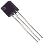
| 描述 | IC TEMP TRANSDUCER 2-TERM TO92-3板上安装温度传感器 Crnt Outpt-Prec IC TEMP Transducer |
| 产品分类 | 温度传感器,变送器温度传感器 |
| 品牌 | Analog Devices Inc |
| 产品手册 | |
| 产品图片 |
|
| rohs | 否含铅 / 不符合限制有害物质指令(RoHS)规范要求 |
| 产品系列 | 板上安装温度传感器,Analog Devices AD592BN- |
| 数据手册 | |
| 产品型号 | AD592BN |
| 产品种类 | 板上安装温度传感器 |
| 供应商器件封装 | TO-92-3 |
| 准确性 | 0.7 C |
| 包装 | 管件 |
| 商标 | Analog Devices |
| 增益 | + 1 uA / K |
| 安装风格 | Through Hole |
| 封装 | Bulk |
| 封装/外壳 | TO-226-3、TO-92-3 标准主体 |
| 封装/箱体 | TO-92-3 |
| 工厂包装数量 | 100 |
| 感应温度 | -25°C ~ 105°C |
| 数字输出-总线接口 | 2-Wire, I2C, SMBus |
| 最大工作温度 | + 105 C |
| 最小工作温度 | - 25 C |
| 标准包装 | 1 |
| 电压-电源 | 4 V ~ 30 V |
| 电源电压-最大 | 30 V |
| 电源电压-最小 | 4 V |
| 精度 | ±0.7°C |
| 系列 | AD592 |
| 设备功能 | Temperature Transducer |
| 输出类型 | 电流 |

,TO-226_straightlead.jpg)


- 商务部:美国ITC正式对集成电路等产品启动337调查
- 曝三星4nm工艺存在良率问题 高通将骁龙8 Gen1或转产台积电
- 太阳诱电将投资9.5亿元在常州建新厂生产MLCC 预计2023年完工
- 英特尔发布欧洲新工厂建设计划 深化IDM 2.0 战略
- 台积电先进制程称霸业界 有大客户加持明年业绩稳了
- 达到5530亿美元!SIA预计今年全球半导体销售额将创下新高
- 英特尔拟将自动驾驶子公司Mobileye上市 估值或超500亿美元
- 三星加码芯片和SET,合并消费电子和移动部门,撤换高东真等 CEO
- 三星电子宣布重大人事变动 还合并消费电子和移动部门
- 海关总署:前11个月进口集成电路产品价值2.52万亿元 增长14.8%


PDF Datasheet 数据手册内容提取
a Low Cost, Precision IC Temperature Transducer AD592 FEATURES CONNECTION DIAGRAM High Precalibrated Accuracy: 0.5(cid:56)C max @ +25(cid:56)C Excellent Linearity: 0.15(cid:56)C max (0(cid:56)C to +70(cid:56)C) Wide Operating Temperature Range: –25(cid:56)C to +105(cid:56)C Single Supply Operation: +4 V to +30 V PIN 3 PIN 2 PIN 1 Excellent Repeatability and Stability High Level Output: 1(cid:109)A/K (–) (NC) (+) Two Terminal Monolithic IC: Temperature In/ *PIN 2 CAN BE EITHER ATTACHED OR UNCONNECTED Current Out BOTTOM VIEW Minimal Self-Heating Errors PRODUCT DESCRIPTION PRODUCT HIGHLIGHTS The AD592 is a two terminal monolithic integrated circuit tem- 1. With a single supply (4 V to 30 V) the AD592 offers perature transducer that provides an output current propor- 0.5(cid:176) C temperature measurement accuracy. tional to absolute temperature. For a wide range of supply 2. A wide operating temperature range (–25(cid:176) C to +105(cid:176) C) voltages the transducer acts as a high impedance temperature and highly linear output make the AD592 an ideal sub- dependent current source of 1m A/K. Improved design and laser stitute for older, more limited sensor technologies (i.e., wafer trimming of the IC’s thin film resistors allows the AD592 thermistors, RTDs, diodes, thermocouples). to achieve absolute accuracy levels and nonlinearity errors previ- ously unattainable at a comparable price. 3. The AD592 is electrically rugged; supply irregularities and variations or reverse voltages up to 20 V will not The AD592 can be employed in applications between –25(cid:176) C damage the device. and +105(cid:176) C where conventional temperature sensors (i.e., ther- mistor, RTD, thermocouple, diode) are currently being used. 4. Because the AD592 is a temperature dependent current The inherent low cost of a monolithic integrated circuit in a source, it is immune to voltage noise pickup and IR plastic package, combined with a low total parts count in any drops in the signal leads when used remotely. given application, make the AD592 the most cost effective tem- 5. The high output impedance of the AD592 provides perature transducer currently available. Expensive linearization greater than 0.5(cid:176) C/V rejection of supply voltage drift and circuitry, precision voltage references, bridge components, resis- ripple. tance measuring circuitry and cold junction compensation are 6. Laser wafer trimming and temperature testing insures not required with the AD592. that AD592 units are easily interchangeable. Typical application areas include: appliance temperature sens- 7. Initial system accuracy will not degrade significantly over ing, automotive temperature measurement and control, HVAC time. The AD592 has proven long term performance (heating/ventilating/air conditioning) system monitoring, indus- and repeatability advantages inherent in integrated cir- trial temperature control, thermocouple cold junction compen- cuit design and construction. sation, board-level electronics temperature diagnostics, temperature readout options in instrumentation, and tempera- ture correction circuitry for precision electronics. Particularly 378 useful in remote sensing applications, the AD592 is immune to voltage drops and voltage noise over long lines due to its high 343 impedance current output. AD592s can easily be multiplexed; the signal current can be switched by a CMOS multiplexer or µA – the supply voltage can be enabled with a tri-state logic gate. UT 1µA/oK O I The AD592 is available in three performance grades: the 273 AD592AN, AD592BN and AD592CN. All devices are pack- aged in a plastic TO-92 case rated from –45(cid:176) C to +125(cid:176) C. Per- 248 formance is specified from –25(cid:176) C to +105(cid:176) C. AD592 chips are also available, contact the factory for details. –45 –25 0 +70 +105+125 TEMPERATURE – oC REV. B Information furnished by Analog Devices is believed to be accurate and reliable. However, no responsibility is assumed by Analog Devices for its use, nor for any infringements of patents or other rights of third parties which may result from its use. No license is granted by implication or One Technology Way, P.O. Box 9106, Norwood, MA 02062-9106, U.S.A. otherwise under any patent or patent rights of Analog Devices. Tel: 781/329-4700 Fax: 781/461-3113
AD592–SPECIFICATIONS (typical @ T = +25(cid:56)C, V = +5 V, unless otherwise noted) A S AD592AN AD592BN AD592CN Model Min Typ Max Min Typ Max Min Typ Max Units ACCURACY Calibration Error @ +25(cid:176) C1 1.5 2.5 0.7 1.0 0.3 0.5 (cid:176) C T = 0(cid:176) C to +70(cid:176) C A Error over Temperature 1.8 3.0 0.8 1.5 0.4 0.8 (cid:176) C Nonlinearity2 0.15 0.35 0.1 0.25 0.05 0.15 (cid:176)C T = –25(cid:176) C to +105(cid:176) C A Error over Temperature3 2.0 3.5 0.9 2.0 0.5 1.0 (cid:176) C Nonlinearity2 0.25 0.5 0.2 0.4 0.1 0.35 (cid:176)C OUTPUT CHARACTERISTICS Nominal Current Output @ +25(cid:176) C (298.2K) 298.2 298.2 298.2 m A Temperature Coefficient 1 1 1 m A/(cid:176) C Repeatability4 0.1 0.1 0.1 (cid:176)C Long Term Stability5 0.1 0.1 0.1 (cid:176)C/month ABSOLUTE MAXIMUM RATINGS Operating Temperature –25 +105 –25 +105 –25 +105 (cid:176)C Package Temperature6 –45 +125 –45 +125 –45 +125 (cid:176) C Forward Voltage (+ to –) 44 44 44 V Reverse Voltage (– to +) 20 20 20 V Lead Temperature (Soldering 10 sec) 300 300 300 (cid:176) C POWER SUPPLY Operating Voltage Range 4 30 4 30 4 30 V Power Supply Rejection +4 V < V < +5 V 0.5 0.5 0.5 (cid:176) C/V S +5 V < V < +15 V 0.2 0.2 0.2 (cid:176) C/V S +15 V < V < +30 V 0.1 0.1 0.1 (cid:176) C/V S NOTES 1An external calibration trim can be used to zero the error @ +25(cid:176)C. 2Defined as the maximum deviation from a mathematically best fit line. 3Parameter tested on all production units at +105(cid:176)C only. C grade at –25(cid:176)C also. 4Maximum deviation between +25(cid:176)C readings after a temperature cycle between –45(cid:176)C and +125(cid:176)C. Errors of this type are noncumulative. 5Operation @ +125(cid:176)C, error over time is noncumulative. 6Although performance is not specified beyond the operating temperature range, temperature excursions within the package temperature range will not damage the device. Specifications subject to change without notice. Specifications shown in boldface are tested on all production units at final electrical test. Results from those tests are used to calculate outgoing quality levels. All min and max specifications are guaranteed, although only those shown in boldface are tested on all production units. METALIZATION DIAGRAM TEMPERATURE SCALE CONVERSION EQUATIONS 66MILS V+ 42MILS V– (cid:56)C = (cid:53)((cid:56)F –32) K = (cid:176) C +273.15 (cid:57) (cid:56)F = (cid:57)(cid:56)C +32 (cid:176) R = (cid:176) F +459.7 (cid:53) –2– REV. B
Typical Performance Curves–AD592 Typical @ V = +5 V S +2.0 +2.0 +1.5 +1.5 +1.0 +1.0 oTOTAL ERROR – C +–00..055 oTOTAL ERROR – C +–00..055 –1.0 –1.0 –1.5 –1.5 –2.0 –2.0 –25 0 +25 +70 +105 –25 0 +25 +70 +105 TEMPERATURE – oC TEMPERATURE – oC AD592CN Accuracy Over Temperature AD592BN Accuracy Over Temperature +2.0 0.75 +1.5 0.50 +1.0 C C 0.25 oR – +0.5 oR – O O R 0 R 0 R R E E L L A –0.5 A OT OT –0.25 T T –1.0 –0.50 –1.5 –2.0 –0.75 –25 0 +25 +70 +105 0 500 1000 1500 2000 TEMPERATURE – oC TIME – Hours AD592AN Accuracy Over Temperature Long-Term Stability @ +85(cid:176)C and 85% Relative Humidity 0.75 0.50 C 0.25 o– R O RR 0 E L A T O–0.25 T –0.50 –0.75 0 500 1000 1500 2000 TIME – Hours Long-Term Stability @ +125(cid:176)C REV. B –3–
AD592 THEORY OF OPERATION resistor. Note that the maximum error at room temperature, The AD592 uses a fundamental property of silicon transistors over the commercial IC temperature range, or an extended to realize its temperature proportional output. If two identical range including the boiling point of water, can be directly read transistors are operated at a constant ratio of collector current from the specifications table. All three error limits are a combi- densities, r, then the difference in base-emitter voltages will be nation of initial error, scale factor variation and nonlinearity de- (kT/q)(ln r). Since both k, Boltzman’s constant and q, the viation from the ideal 1m A/K output. Figure 2 graphically charge of an electron are constant, the resulting voltage is depicts the guaranteed limits of accuracy for an AD592CN. directly Proportional To Absolute Temperature (PTAT). In the AD592 this difference voltage is converted to a PTAT current +1.0 by low temperature coefficient thin film resistors. This PTAT current is then used to force the total output current to be pro- +0.5 MAXIMUM ERROR portional to degrees Kelvin. The result is a current source with OVER TEMPERATURE C an output equal to a scale factor times the temperature (K) of o– TYPICAL ERROR the sensor. A typical V-I plot of the circuit at +25(cid:176) C and the OR 0 temperature extremes is shown in Figure 1. RR CALIBRATION E ERROR LIMIT L TA –0.5 O T MAXIMUM ERROR –1.0 OVER TEMPERATURE +105oC 378 – µA 298 +25oC –25 0 TE+M25PERATURE – oC +70 +105 OUT 248 –25oC I Figure 2.Error Specifications (AD592CN) UP TO 30V The AD592 has a highly linear output in comparison to older technology sensors (i.e., thermistors, RTDs and thermo- couples), thus a nonlinearity error specification is separated from the absolute accuracy given over temperature. As a maxi- 0 1 2 3 4 5 6 mum deviation from a best-fit straight line this specification rep- SUPPLY VOLTAGE – Volts resents the only error which cannot be trimmed out. Figure 3 is Figure 1.V-I Characteristics a plot of typical AD592CN nonlinearity over the full rated tem- perature range. Factory trimming of the scale factor to 1m A/K is accomplished at the wafer level by adjusting the AD592’s temperature reading +0.2 so it corresponds to the actual temperature. During laser trim- ming the IC is at a temperature within a few degrees of 25(cid:176) C and is powered by a 5V supply. The device is then packaged +0.1 TYPICAL NONLINEARITY and automatically temperature tested to specification. C o FACTORS AFFECTING AD592 SYSTEM PRECISION TY – 0 RI The accuracy limits given on the Specifications page for the A E AD592 make it easy to apply in a variety of diverse applications. LIN –0.1 N To calculate a total error budget in a given system it is impor- O N tant to correctly interpret the accuracy specifications, non- –0.2 linearity errors, the response of the circuit to supply voltage variations and the effect of the surrounding thermal environ- ment. As with other electronic designs external component se- –25 0 +25 +70 +105 lection will have a major effect on accuracy. TEMPERATURE – oC CALIBRATION ERROR, ABSOLUTE ACCURACY AND Figure 3.Nonlinearity Error (AD592CN) NONLINEARITY SPECIFICATIONS Three primary limits of error are given for the AD592 such that TRIMMING FOR HIGHER ACCURACY the correct grade for any given application can easily be chosen Calibration error at 25(cid:176) C can be removed with a single tempera- for the overall level of accuracy required. They are the calibra- ture trim. Figure 4 shows how to adjust the AD592’s scale fac- tion accuracy at +25(cid:176) C, and the error over temperature from tor in the basic voltage output circuit. 0(cid:176) C to +70(cid:176) C and –25(cid:176) C to +105(cid:176) C. These specifications cor- respond to the actual error the user would see if the current out- put of an AD592 were converted to a voltage with a precision –4– REV. B
AD592 +V SUPPLY VOLTAGE AND THERMAL ENVIRONMENT EFFECTS AD592 The power supply rejection characteristics of the AD592 mini- mizes errors due to voltage irregularity, ripple and noise. If a supply is used other than 5V (used in factory trimming), the R 100W power supply error can be removed with a single temperature VOUT = 1mV/K trim. The PTAT nature of the AD592 will remain unchanged. 950W The general insensitivity of the output allows the use of lower cost unregulated supplies and means that a series resistance of several hundred ohms (e.g., CMOS multiplexer, meter coil Figure 4. Basic Voltage Output (Single Temperature Trim) resistance) will not degrade the overall performance. To trim the circuit the temperature must be measured by a ref- +2.0 erence sensor and the value of R should be adjusted so the out- put (V ) corresponds to 1mV/K. Note that the trim OUT procedure should be implemented as close as possible to the +1.0 temperature highest accuracy is desired for. In most applications C if a single temperature trim is desired it can be implemented oR – 0 where the AD592 current-to-output voltage conversion takes O R place (e.g., output resistor, offset to an op amp). Figure 5 illus- ER L trates the effect on total error when using this technique. A–1.0 T O T +1.0 –2.0 ACCURACY WITHOUT TRIM +0.5 –25 0 +25 +75 +105 oR – C 0 TEMPERATURE – oC O R AFTER SINGLE Figure 7. Typical Two Trim Accuracy ER TEMPERATURE L CALIBRATION The thermal environment in which the AD592 is used deter- A–0.5 T O mines two performance traits: the effect of self-heating on accu- T racy and the response time of the sensor to rapid changes in –1.0 temperature. In the first case, a rise in the IC junction tempera- ture above the ambient temperature is a function of two vari- ables; the power consumption level of the circuit and the –25 +25 +105 thermal resistance between the chip and the ambient environ- TEMPERATURE – oC ment (q ). Self-heating error in (cid:176) C can be derived by multiply- JA ing the power dissipation by q . Because errors of this type can Figure 5.Effect of Scale Factor Trim on Accuracy JA vary widely for surroundings with different heat sinking capaci- If greater accuracy is desired, initial calibration and scale factor ties it is necessary to specify q under several conditions. Table JA errors can be removed by using the AD592 in the circuit of I shows how the magnitude of self-heating error varies relative Figure 6. to the environment. In typical free air applications at +25(cid:176) C with a 5V supply the magnitude of the error is 0.2(cid:176) C or less. A R2 5kW common clip-on heat sink will reduce the error by 25% or more 97.6kW +5V R1 in critical high temperature, large supply voltage situations. 8.66kW 1kW AD741 AD1403 Table I. Thermal Characteristics 7.87kW VOUT = 100mV/oC Medium q JA ((cid:176)C/watt) t (sec)* AD592 Still Air Without Heat Sink 175 60 V– With Heat Sink 130 55 Figure 6.Two Temperature Trim Circuit Moving Air With the transducer at 0(cid:176) C adjustment of R1 for a 0V output Without Heat Sink 60 12 With Heat Sink 40 10 nulls the initial calibration error and shifts the output from K to (cid:176) C. Tweaking the gain of the circuit at an elevated temperature Fluorinert Liquid 35 5 Aluminum Block** 30 2.4 by adjusting R2 trims out scale factor error. The only error remaining over the temperature range being trimmed for is NOTES nonlinearity. A typical plot of two trim accuracy is given in *t is an average of five time constants (99.3% of final value). In cases where the Figure 7. thermal response is not a simple exponential function, the actual thermal re- sponse may be better than indicated. **With thermal grease. REV. B –5–
AD592 Response of the AD592 output to abrupt changes in ambient +5V +15V temperature can be modeled by a single time constant t expo- nential function. Figure 8 shows typical response time plots for AD592 several media of interest. AD592 AD592 100 A C 90 B D AD592 E 80 3(303.1.3%W) VTAVG (1mV/K) ATUR 70 E (01.01k%W) VTAVG (10mV/K) R F E P 60 EM A ALUMINUM BLOCK FINAL T 5400 BCD FMMLOOUVVOIINNRGGIN AAEIIRRRT (( WWLIQIITTUHHI ODHUETA TH ESAINTK S)INK) Figure 9.Average and Minimum Temperature F E STILL AIR (WITH HEAT SINK) Connections T O 30 F STILL AIR (WITHOUT HEAT SINK) N The circuit of Figure 10 demonstrates a method in which a RCE 20 voltage output can be derived in a differential temperature E P 10 measurement. 0 20 40 60 80 100120140160180200220240260280300 +V TIME – sec 10kW Figure 8. Thermal Response Curves AD592 The time constant, t , is dependent on q and the thermal ca- AD741 JA pacities of the chip and the package. Table I lists the effective t 5MW R1 (time to reach 63.2% of the final value) for several different AD592 50kW VOUT = (T1 – T2) x media. Copper printed circuit board connections where ne- 10kW (10mV/oC) glected in the analysis, however, they will sink or conduct heat –V directly through the AD592’s solder dipped Kovar leads. When faster response is required a thermally conductive grease or glue Figure 10.Differential Measurements between the AD592 and the surface temperature being mea- R1 can be used to trim out the inherent offset between the two sured should be used. In free air applications a clip-on heat sink devices. By increasing the gain resistor (10kW ) temperature will decrease output stabilization time by 10-20%. measurements can be made with higher resolution. If the magni- tude of V+ and V– is not the same, the difference in power con- MOUNTING CONSIDERATIONS sumption between the two devices can cause a differential If the AD592 is thermally attached and properly protected, it self-heating error. can be used in any temperature measuring situation where the maximum range of temperatures encountered is between –25(cid:176) C Cold junction compensation (CJC) used in thermocouple signal and +105(cid:176) C. Because plastic IC packaging technology is em- conditioning can be implemented using an AD592 in the circuit ployed, excessive mechanical stress must be safeguarded against configuration of Figure 11. Expensive simulated ice baths or when fastening the device with a clamp or screw-on heat tab. hard to trim, inaccurate bridge circuits are no longer required. Thermally conductive epoxy or glue is recommended under typical mounting conditions. In wet or corrosive environments, THERMOCOUPLE APPROX. TYPE R VALUE any electrically isolated metal or ceramic well can be used to shield the AD592. Condensation at cold temperatures can cause +7.5V JK 5421WW leakage current related errors and should be avoided by sealing T 41W E 61W the device in nonconductive epoxy paint or dips. 2.5V S 6W AD1403 R 6W MEASURING APPLICATIONS JUNCTION 10kW AD OP07E Connecting several AD592 devices in parallel adds the currents Cu 1kW VOUT through them and produces a reading proportional to the aver- age temperature. Series AD592s will indicate the lowest tem- AD592 100kW RG2 perature because the coldest device limits the series current Cu REJFUENRCETNIOCNE (1kW) RG1 flowing through the sensors. Both of these circuits are depicted in Figure 9. R Figure 11. Thermocouple Cold Junction Compensation –6– REV. B
AD592 The circuit shown can be optimized for any ambient tempera- By using a differential input A/D converter and choosing the ture range or thermocouple type by simply selecting the correct current to voltage conversion resistor correctly, any range of value for the scaling resistor – R. The AD592 output (1m A/K) temperatures (up to the 130(cid:176) C span the AD592 is rated for) times R should approximate the line best fit to the thermocouple centered at any point can be measured using a minimal number curve (slope in V/(cid:176) C) over the most likely ambient temperature of components. In this configuration the system will resolve up range. Additionally, the output sensitivity can be chosen by to 1(cid:176) C. selecting the resistors R and R for the desired noninverting G1 G2 A variable temperature controlling thermostat can easily be built gain. The offset adjustment shown simply references the AD592 using the AD592 in the circuit of Figure 14. to (cid:176) C. Note that the TC’s of the reference and the resistors are the primary contributors to error. Temperature rejection of 40 +15V to 1 can be easily achieved using the above technique. Although the AD592 offers a noise immune current output, it is AD581 not compatible with process control/industrial automation cur- RPULL-UP rent loop standards. Figure 12 is an example of a temperature to 4–20mA transmitter for use with 40V, 1kW systems. 6R2.H7IkGWH AD592 COMPARATOR In this circuit the 1m A/K output of the AD592 is amplified to RSET TOEUMTPP U>T S HEITGPHOINT 1mA/(cid:176) C and offset so that 4mA is equivalent to 17(cid:176) C and 10kW 20mA is equivalent to 33(cid:176) C. Rt is trimmed for proper reading TEMP < SETPOINT OUTPUT LOW at an intermediate reference temperature. With a suitable choice RHYST of resistors, any temperature range within the operating limits of 10kW C RLOW (OPTIONAL) the AD592 may be chosen. 27.3kW C +20V AD581 17(cid:176)C » 4mA Figure 14.Variable Temperature Thermostat 33(cid:176)C » 20µA 35.7kW 1mA/oC RHIGH and RLOW determine the limits of temperature controlled by the potentiometer R . The circuit shown operates over the SET AD592 10mV/oC RT full temperature range (–25(cid:176) C to +105(cid:176) C) the AD592 is rated 5kW 208 for. The reference maintains a constant set point voltage and insures that approximately 7V appears across the sensor. If it is necessary to guardband for extraneous noise hysteresis can be C 10kW 12.7kW 5kW 500W added by tying a resistor from the output to the ungrounded end of R LOW. 10W VT Multiple remote temperatures can be measured using several –20V AD592s with a CMOS multiplexer or a series of 5V logic gates because of the device’s current-mode output and supply-voltage Figure 12.Temperature to 4–20mA Current Transmitter compliance range. The on-resistance of a FET switch or output Reading temperature with an AD592 in a microprocessor based impedance of a gate will not affect the accuracy, as long as 4V system can be implemented with the circuit shown in Figure 13. is maintained across the transducer. MUXs and logic driving circuits should be chosen to minimize leakage current related +5V errors. Figure 15 illustrates a locally controlled MUX switching the signal current from several remote AD592s. CMOS or TTL BPO/UPO gates can also be used to switch the AD592 supply voltages, AD592 FORMAT VCC with the multiplexed signal being transmitted over a single VI N HI twisted pair to the load. AD670 AD1403 VI N LO ADCPORT +15V –15V 8 BITS 9kW OUT STPRAIMN 190500WW 200W CPTROEINIMNTTER VVI NI N L HOI GND T8 T2 T1 RAEDM59O2TsESS12 AD7501 ODEC DRI 1V0kOWUT 1kW D V R/W CS CE E E S8 R R / µP CONTROL TTL DTL TO CMOS I/O Figure 13.Temperature to Digital Output EN CHANNEL SELECT Figure 15.Remote Temperature Multiplexing REV. B –7–
AD592 To minimize the number of MUXs required when a large num- To convert the AD592 output to (cid:176) C or (cid:176) F a single inexpensive ber of AD592s are being used, the circuit can be configured in a reference and op amp can be used as shown in Figure 17. Al- matrix. That is, a decoder can be used to switch the supply volt- though this circuit is similar to the two temperature trim circuit age to a column of AD592s while a MUX is used to control shown in Figure 6, two important differences exist. First, the which row of sensors are being measured. The maximum num- gain resistor is fixed alleviating the need for an elevated tem- ber of AD592s which can be used is the product of the number perature trim. Acceptable accuracy can be achieved by choosing of channels of the decoder and MUX. an inexpensive resistor with the correct tolerance. Second, the AD592 calibration error can be trimmed out at a known conve- An example circuit controlling 80 AD592s is shown in Figure nient temperature (i.e., room temperature) with a single pot ad- 16. A 7-bit digital word is all that is required to select one of justment. This step is independent of the gain selection. the sensors. The enable input of the multiplexer turns all the sensors off for minimum dissipation while idling. ROFFSET RGAIN CSOELLUECMTN +5V ROFFSET RGAIN ooCF » » 99..18kk WW 110800kkWW R RCAL AD741 2.5V +15V ROW AD1403 4028 BCD TO DECIMAL DECODER SELECT ROFFSET/RGAIN VOUT = 100mV/(oC OR oF) AD592 VOUT V– UX 10kW M D7501NNEL Figure 17.Celsius or Fahrenheit Thermometer AA H C 8- +15V –15V EN 80 – AD592s Figure 16.Matrix Multiplexer –8– REV. B
AD592 OUTLINE DIMENSIONS 0.165 (4.19) 0.210 (5.33) 0.145 (3.68) 0.190 (4.83) 0.125 (3.18) 0.170 (4.32) 00..00212805 ((00..5467)) 0.055 (1.40) 00..10195705 ((22..9428)) 0.0150 (0.38) 0.050 (1.27) 0.0800 (2.03) 0.045 (1.15) 3 0.205 (5.21) 0.190 (4.83) 2 0.175 (4.45) 0.105 (2.68) 1 0.100 (2.54) 0.020 (0.51) FRONT VIEW 0.500 (12.70) MIN 0.095 (2.42) 0.017 (0.43) 0.014 (0.36) SEATING BOTTOM VIEW PLANE COMPLIANT TO JEDEC STANDARDS TO-226-AA C(RINOE FNPETARRREOENLNCLTEIHN OEGSN DELISYM) AEANNRSDEI OARRNOESU NANORDEET D IAN-PO IPFNRFCO HEPEQRSUI;AI VMTAIELL LFEIONMTRES TU EFSORE R DINIM DEENSSIGIONN.S 042208-A Figure 18. 3-Pin Plastic Header-Style Package [TO-92] (T-3-1) Dimensions shown in inches and (millimeters) ORDERING GUIDE Model1 Temperature Range Package Description Package Option AD592AN −25°C to +105°C 3-Pin Plastic Header-Style Package [TO-92] T-3-1 AD592ANZ −25°C to +105°C 3-Pin Plastic Header-Style Package [TO-92] T-3-1 AD592BN −25°C to +105°C 3-Pin Plastic Header-Style Package [TO-92] T-3-1 AD592BNZ −25°C to +105°C 3-Pin Plastic Header-Style Package [TO-92] T-3-1 AD592CN −25°C to +105°C 3-Pin Plastic Header-Style Package [TO-92] T-3-1 AD592CNZ −25°C to +105°C 3-Pin Plastic Header-Style Package [TO-92] T-3-1 AD592ACHIPS 0°C to 70°C 1 Z = RoHS Compliant Part. REVISION HISTORY 6/15—Rev. A to Rev. B Updated Outline Dimensions .......................................................... 9 Changes to Ordering Guide ............................................................. 9 ©2015 Analog Devices, Inc. All rights reserved. Trademarks and registered trademarks are the property of their respective owners. D09374-0-6/15(B) Rev. B | Page 9