ICGOO在线商城 > 集成电路(IC) > PMIC - 电压基准 > AD589JH
 Datasheet下载
- 型号: AD589JH
- 制造商: Analog
- 库位|库存: xxxx|xxxx
- 要求:
| 数量阶梯 | 香港交货 | 国内含税 |
| +xxxx | $xxxx | ¥xxxx |
查看当月历史价格
查看今年历史价格
AD589JH产品简介:
ICGOO电子元器件商城为您提供AD589JH由Analog设计生产,在icgoo商城现货销售,并且可以通过原厂、代理商等渠道进行代购。 AD589JH价格参考。AnalogAD589JH封装/规格:PMIC - 电压基准, 分流器 电压基准 IC -2.83%,+1.22% 5mA TO-51-2。您可以下载AD589JH参考资料、Datasheet数据手册功能说明书,资料中有AD589JH 详细功能的应用电路图电压和使用方法及教程。
AD589JH是由Analog Devices Inc.生产的精密电压基准芯片,属于PMIC(电源管理集成电路)中的电压基准类别。它广泛应用于需要高精度、低温度漂移和稳定电压输出的场景。以下是AD589JH的主要应用场景:

1. 数据转换系统:
   AD589JH常用于ADC(模数转换器)和DAC(数模转换器)的参考电压源。其高精度和低漂移特性确保了数据转换系统的准确性和可靠性,适用于工业控制、医疗设备和测试测量仪器。

2. 电源监控与管理:
   在电源管理系统中,AD589JH可用作电压基准,监测和调节输出电压,确保系统在不同负载条件下保持稳定的供电。例如,电池管理系统(BMS)中使用它来精确测量电池电压。

3. 工业自动化与控制:
   工业自动化设备需要高精度的传感器信号处理,AD589JH可以为这些设备提供稳定的基准电压,从而提高测量精度和控制性能。

4. 通信设备:
   在通信领域,AD589JH可用于射频(RF)功率放大器的偏置电路或信号链中的基准电压源,以保证信号传输的稳定性和准确性。

5. 医疗设备:
   医疗设备如心电图仪、血压监测仪等对精度要求极高,AD589JH能够为这些设备提供可靠的基准电压,确保测量结果的准确性。

6. 测试与测量仪器:
   示波器、万用表和其他测试设备需要高精度的基准电压源,AD589JH因其优异的性能成为理想选择。

7. 汽车电子:
   在汽车电子系统中,AD589JH可用于传感器信号调理、发动机控制单元(ECU)以及车载信息娱乐系统的电压基准。

总之,AD589JH凭借其高精度、低温漂和稳定性,适用于各种对电压基准要求严格的场合,特别是在需要长期稳定性和高可靠性的应用中表现出色。
| 参数 | 数值 |
| 产品目录 | 集成电路 (IC)半导体 |
| 描述 | IC VREF SHUNT 1.235V TO-51-2参考电压 2-Terminal IC 1.2V REF |
| 产品分类 | |
| 品牌 | Analog Devices |
| 产品手册 | |
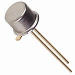
| 产品图片 |
|
| rohs | 符合RoHS无铅 / 符合限制有害物质指令(RoHS)规范要求 |
| 产品系列 | 电源管理 IC,参考电压,Analog Devices AD589JH- |
| 数据手册 | |
| 产品型号 | AD589JH |
| 产品目录页面 | |
| 产品种类 | 参考电压 |
| 供应商器件封装 | TO-51-2 |
| 分流电流—最大值 | 5 mA |
| 分流电流—最小值 | 50 uA |
| 初始准确度 | 1.2 % |
| 包装 | 散装 |
| 参考类型 | Shunt References |
| 商标 | Analog Devices |
| 安装类型 | 通孔 |
| 安装风格 | Through Hole |
| 容差 | -2.83%, +1.22% |
| 封装 | Bulk |
| 封装/外壳 | TO-51-2 金属罐 |
| 封装/箱体 | TO-51-2 |
| 工作温度 | 0°C ~ 70°C |
| 工厂包装数量 | 100 |
| 平均温度系数—典型值 | 100 PPM / C |
| 最大工作温度 | + 125 C |
| 最小工作温度 | - 55 C |
| 标准包装 | 1 |
| 温度系数 | 100ppm/°C |
| 电压-输入 | - |
| 电压-输出 | 1.235V |
| 电流-输出 | 5mA |
| 电流-阴极 | 5mA |
| 电流-静态 | - |
| 系列 | AD589 |
| 输出电压 | 1.2 V |
| 通道数 | 1 |


- 商务部:美国ITC正式对集成电路等产品启动337调查
- 曝三星4nm工艺存在良率问题 高通将骁龙8 Gen1或转产台积电
- 太阳诱电将投资9.5亿元在常州建新厂生产MLCC 预计2023年完工
- 英特尔发布欧洲新工厂建设计划 深化IDM 2.0 战略
- 台积电先进制程称霸业界 有大客户加持明年业绩稳了
- 达到5530亿美元!SIA预计今年全球半导体销售额将创下新高
- 英特尔拟将自动驾驶子公司Mobileye上市 估值或超500亿美元
- 三星加码芯片和SET,合并消费电子和移动部门,撤换高东真等 CEO
- 三星电子宣布重大人事变动 还合并消费电子和移动部门
- 海关总署:前11个月进口集成电路产品价值2.52万亿元 增长14.8%


PDF Datasheet 数据手册内容提取
2-Terminal IC 1.2 V Reference AD589 FEATURES FUNCTIONAL BLOCK DIAGRAMS Superior Replacement for Other 1.2 V References Wide Operating Range: 50 A to 5 mA SOIC (R-8) Metal Can (H-02) Low Power: 60 W Total P at 50 A D Low Temperature Coeffi cient: �� 10 ppm/C Max, 0C to 70C (AD589M) 1 8 +V 2-Terminal Zener Operation 2 7 Low Output Impedance: 0.6 3 6 No Frequency Compensation Required –V 4 5 AD589 Low Cost �� TOPVIEW MIL-STD-883 Compliant Versions Available (NottoScale) ���������� PRODUCT DESCRIPTION PRODUCT HIGHLIGHTS The AD589 is a 2-terminal, low cost, temperature compensated 1. The AD589 is a 2-terminal device that delivers a constant band gap voltage reference that provides a fi xed 1.23 V output reference voltage for a wide range of input current. voltage for input currents between 50 A and 5.0 mA. 2. Output impedance of 0.6 and temperature coeffi cients as The high stability of the AD589 is primarily dependent upon low as 10 ppm/°C ensure stable output voltage over a wide the matching and thermal tracking of the on-chip components. range of operating conditions. Analog Devices’ precision bipolar processing and thin-fi lm tech- 3. The AD589 can be operated as a positive or negative refer- nology combine to provide excellent performance at low cost. ence. Floating operation is also possible. Additionally, the active circuit produces an output impedance 10 4. The AD589 will operate with a total current as low as 50 A lower than the typical low-TC Zener diodes. This feature allows (60 W total power dissipation), ideal for battery-powered operation with no external components required to maintain full instrument applications. accuracy under changing load conditions. 5. The AD589 is an exact replacement for other 1.2 V references, The AD589 is available in seven versions. The AD589J, AD589K, offering superior temperature performance and reduced sensi- AD589L, and AD589M grades are specifi ed for 0°C to +70°C tivity to capacitive loading. operation, while the AD589S and AD589T grades are rated for the full –55°C to +125°C temperature range. All grades are avail- 6. The AD589 is available in versions compliant with MIL- able in a metal can (H-02) package. The AD589J is also available STD-883. Consult factory for 883 data sheet. in an 8-lead SOIC package. REV. C Information furnished by Analog Devices is be lieved to be accurate and reliable. However, no responsibility is assumed by Analog Devices for its use, nor for any infringements of patents or other rights of third parties that may result from its use. No license is granted by implication or oth- One Technology Way, P.O. Box 9106, Norwood, MA 02062-9106, U.S.A. erwise under any patent or patent rights of Analog Devices. Trademarks Tel: 781/329-4700 www.analog.com and registered trademarks are the property of their respective owners. Fax: 781/326-8703 © 2004 Analog Devices, Inc. All rights reserved.
AD589–SPECIFICATIONS (Typical @ I = 500 A and T = 25C, unless otherwise noted.) IN A AD589JH/ Model AD589JR AD589KH AD589LH AD589MH Min Typ Max Min Typ Max Min Typ Max Min Typ Max Unit OUTPUT VOLTAGE, T = 25°C 1.200 1.235 1.250 1.200 1.235 1.250 1.200 1.235 1.250 1.200 1.235 1.250 V A OUTPUT VOLTAGE CHANGE VERSUS CURRENT 50 A to 5 mA 5 5 5 5 mV DYNAMIC OUTPUT IMPEDANCE 0.6 2 0.6 2 0.6 2 0.6 2 RMS NOISE VOLTAGE 10 Hz < f < 10 kHz 5 5 5 5 V TEMPERATURE COEFFICIENT1 100 50 25 10 ppm/°C TURN-ON SETTLING TIME TO 0.1% 25 25 25 25 s OPERATING CURRENT2 0.05 5 0.05 5 0.05 5 0.05 5 mA OPERATING TEMPERATURE 0 70 0 70 0 70 0 70 °C PACKAGE OPTION3 Metal Can (H-02A) AD589JH AD589KH AD589LH AD589MH SOIC (R-8) AD589JR Model AD589SH AD589TH Min Typ Max Min Typ Max Unit OUTPUT VOLTAGE, T = 25°C 1.200 1.235 1.250 1.200 1.235 1.250 V A OUTPUT VOLTAGE CHANGE VERSUS CURRENT 50 A to 5 mA 5 5 mV DYNAMIC OUTPUT IMPEDANCE 0.6 2 0.6 2 RMS NOISE VOLTAGE 10 Hz < f < 10 kHz 5 5 V TEMPERATURE COEFFICIENT1 100 50 ppm/°C TURN-ON SETTLING TIME TO 0.1% 25 25 s OPERATING CURRENT2 0.05 5 0.05 5 mA OPERATING TEMPERATURE –55 +125 –55 +125 °C PACKAGE OPTION3 Metal Can (H-02) AD589SH AD589TH SOIC (R-8) AD589JR NOTES 1See the Voltage Variation versus Temperature section for explanation of temperature coeffi cient measurement method. 2Optimum performance is obtained at currents below 500 A. For current operation below 200 A, stray shunt capacitances should be limited to 20 pF or increased to 1 F. If strays cannot be avoided, operation at 500 A and a shunt capacitor of at least 1000 pF are recommended. 3H = Hermetic Metal Can; R = SOIC. Specifi cations shown in boldface are tested on all production units at fi nal electrical test. Specifi cations subject to change without notice. –2– REV. C
AD589 ABSOLUTE MAXIMUM RATINGS AD589 CHIP DIMENSIONS AND PAD LAYOUT Current . . . . . . . . . . . . . . . . . . . . . . . . . . . . . . . . . . . . . 10 mA Reverse Current . . . . . . . . . . . . . . . . . . . . . . . . . . . . . . . 10 mA Power Dissipation* . . . . . . . . . . . . . . . . . . . . . . . . . . .125 mW Storage Temperature . . . . . . . . . . . . . . . . . . . .–65°C to +175°C Operating Junction Temperature Range . . . . . .–55°C to +150°C Lead Temperature (Soldering, 10 sec) . . . . . . . . . . . . . . . .300°C ����� ������� *Absolute maximum power dissipation is limited by maximum current through the device. Maximum rating at elevated temperatures must be computed assuming TTTJJ 150°C andJA = 400 = C/W. ����� ������� �������������������������������������������� ��������������������������������������������� �������������������������� ORDERING GUIDE Temperature No. of Parts Per Temperature Model Coeffi cient (ppm/C) Package Description Package Option Reel/Tray Range (C) AD589JH 100 Metal Can (TO-51) H-02 100 0 to +70 AD589JR 100 SOIC-8 R-8 98 0 to +70 AD589JRZ* 100 SOIC-8 R-8 98 0 to +70 AD589JR-REEL 100 SOIC-8 R-8 2,500 0 to +70 AD589JRZ-REEL* 100 SOIC-8 R-8 2,500 0 to +70 AD589JCHIPS 100 DICE — 25 0 to +70 AD589KH 50 Metal Can (TO-51) H-02 100 0 to +70 AD589LH 25 Metal Can (TO-51) H-02 100 0 to +70 AD589MH 10 Metal Can (TO-51) H-02 100 0 to +70 AD589SH 100 Metal Can (TO-51) H-02 100 –55 to +125 AD589SH/883B 100 Metal Can (TO-51) H-02 100 –55 to +125 AD589TH 50 Metal Can (TO-51) H-02 100 –55 to +125 AD589TH/883B 50 Metal Can (TO-51) H-02 100 –55 to +125 AD589TCHIPS 50 DICE — 25 –55 to +125 *Z = Pb-free part CAUTION ESD (electrostatic discharge) sensitive device. Electrostatic charges as high as 4000 V readily ac cu mu late on the human body and test equipment and can discharge without detection. Although the AD589 features proprietary ESD pro tec tion circuitry, permanent damage may occur on devices subjected to high energy electrostatic discharges. Therefore, proper ESD pre cau tions are rec om mend ed to avoid per for mance deg ra da tion or loss of functionality. REV. C –3–
AD589 UNDERSTANDING THE SPECIFICATIONS Dynamic Performance Voltage Variation Versus Temperature Many low power instrument manufacturers are becoming increas- Some confusion exists in the area of defi ning and specifying ingly concerned with the turn-on characteristics of the components reference voltage error over temperature. Historically, references being used in their systems. Fast turn-on components often enable have been characterized using a maximum deviation per degree the end user to keep power off when not needed and yet respond Centigrade, i.e., 10 ppm/°C. However, because of nonlinearities quickly when the power is turned on for operation. Figure 3 dis- in temperature characteristics, which originated in standard Zener plays the turn-on characteristics of the AD589. This characteristic references (such as S type characteristics), most manufacturers is generated from cold-start operation and represents the true turn- have begun to use a maximum limit error band approach to specify on waveform after an extended period with the supplies off. The devices. This technique involves measurement of the output at fi gure shows both the coarse and fi ne transient characteristics of 3, 5, or more different temperatures to guarantee that the output the device; the total settling time to within ±1 mV is about 25 s, voltage will fall within the given error band. The temperature and there is no long thermal tail appearing after that point. characteristics of the AD589 consistently follows the curve shown in Figure 1. Three-point measurement guarantees the error band over the specifi ed temperature range. The temperature coeffi cients ����� ���� ���� specifi ed in the Specifi cations section represent the slopes of the ��� �� diagonals of the error band from 25°C to T and 25°C to T . MIN MAX ������ ������ �� �� �� � � � ������� � � � � Figure 3. Output Settling Characteristics � �������� � � �� � �� �� �� ������ �� ������ �� ��� ��� � �� �� �� ��� ��� ��������������� �� �� �� �� �� �� Figure 1. Typical AD589 Temperature Characteristics �� ���� �� �� �� �� ��� �� �� � ���� Figure 4. Schematic Diagram � � �� � � � � � � � � �� � � � � � �� � � �� �� �� ��� ���� � ������������� Figure 2. Noise Spectral Density –4– REV. C
AD589 APPLICATION INFORMATION �� The AD589 functions as a 2-terminal shunt-type regulator. It ����� provides a constant 1.23 V output for a wide range of input current from 50 A to 5 mA. Figure 5 shows the simplest con- ����� �� ���� fi guration for an output voltage of 1.2 V or less. Note that no ����� ��� ���� frequency compensation is required. If additional fi ltering is ���� desired for ultralow noise applications, minimum recommended capacitance is 1000 pF. ������ �� ����� a. With 7109 12-Bit Binary ADC �� ����� ���� ����� ���� �� ���� ���� ����� Figure 5. Basic Confi guration for 1.2 V or Less ��� ����� The AD589 can also be used as a building block to generate ����� other values of reference voltage. Figure 6 shows a circuit that ������ produces a buffered 10 V output. Total supply current for this circuit is approximately 2 mA. ����� b. With 7107 Panel Meter ADC ��� Figure 7. AD589 Used as Reference for CMOS ADCs The AD589 also is useful as a reference for CMOS multiplying ���� � � DACs, such as the AD7533. These DACs require a negative ������ � reference voltage in order to provide a positive output range. � � ��� Figure 8 shows the AD589 used to supply an equivalent –1.0 V � � ��� reference to an AD7533. ������ ��� ��� ��� � � � � � � � � � �� ��� ��� ����� ��� ����� ���� �� ��� ������������ Figure 6. Single-Supply Buffered 10 V Reference �� �� The low power operation of the AD589 makes it ideal for use in �� ��� ��� ���W � battery-operated portable equipment. It is especially useful as a � � �� reference for CMOS analog-to-digital converters. Figure 7 shows ���� the AD589 used in conjunction with two popular integrating type ���� ���� ��� CMOS ADCs. ����� �������� ������ Figure 8. AD589 as Reference for 10-Bit CMOS DAC REV. C –5–
AD589 OUTLINE DIMENSIONS 8-Lead Standard Small Outline Package [SOIC] Narrow Body (R-8) Dimensions shown in millimeters and (inches) 5.00 (0.1968) 4.80 (0.1890) 8 5 4.00 (0.1574) 6.20 (0.2440) 3.80 (0.1497) 1 4 5.80 (0.2284) 1.27 (0.0500) 0.50 (0.0196) BSC 1.75 (0.0688) 0.25 (0.0099) 45 0.25 (0.0098) 1.35 (0.0532) 0.10 (0.0040) 0.51 (0.0201) 8 COPLANARITY 0.31 (0.0122) 0.25 (0.0098)0 1.27 (0.0500) 0.10 SEPALTAINNGE 0.17 (0.0067) 0.40 (0.0157) COMPLIANT TO JEDEC STANDARDS MS-012AA CONTROLLING DIMENSIONS ARE IN MILLIMETERS; INCH DIMENSIONS (IN PARENTHESES) ARE ROUNDED-OFF MILLIMETER EQUIVALENTS FOR REFERENCE ONLY AND ARE NOT APPROPRIATE FOR USE IN DESIGN 2-Pin Metal Header Package [TO-51] (H-02) Dimensions shown in inches and (millimeters) 0.230 (5.84) DIA 0.209 (5.31) 0.10 (2.54) 0.195 (4.95)DIA 0.150 (3.81) 0.178 (4.52) 0.125 (3.17) 45° 0.048 (1.22) 0.028 (0.71) 0.500 (12.7) 0.019 (0.48) MIN 0.046 (1.17) 0.015 (0.38) 0.036 (0.91) CONTROLLING DIMENSIONS ARE IN INCHES; MILLIMETERS DIMENSIONS (IN PARENTHESES) ARE ROUNDED-OFF EQUIVALENTS FOR REFERENCE ONLY AND ARE NOT APPROPRIATE FOR USE IN DESIGN –6– REV. C
AD589 Revision History Location Page 2/04 —Data Sheet changed from REV. B to REV. C Changes to FEATURES . . . . . . . . . . . . . . . . . . . . . . . . . . . . . . . . . . . . . . . . . . . . . . . . . . . . . . . . . . . . . . . . . . . . . . . . . . . . . . . . . . . 1 Changes to PRODUCT DESCRIPTION . . . . . . . . . . . . . . . . . . . . . . . . . . . . . . . . . . . . . . . . . . . . . . . . . . . . . . . . . . . . . . . . . . . . . 1 Changes to PRODUCT HIGHLIGHTS . . . . . . . . . . . . . . . . . . . . . . . . . . . . . . . . . . . . . . . . . . . . . . . . . . . . . . . . . . . . . . . . . . . . . . 1 Changes to SPECIFICATIONS . . . . . . . . . . . . . . . . . . . . . . . . . . . . . . . . . . . . . . . . . . . . . . . . . . . . . . . . . . . . . . . . . . . . . . . . . . . . . 2 Added ORDERING GUIDE . . . . . . . . . . . . . . . . . . . . . . . . . . . . . . . . . . . . . . . . . . . . . . . . . . . . . . . . . . . . . . . . . . . . . . . . . . . . . . . 3 Updated OUTLINE DIMENSIONS . . . . . . . . . . . . . . . . . . . . . . . . . . . . . . . . . . . . . . . . . . . . . . . . . . . . . . . . . . . . . . . . . . . . . . . . . 6 REV. C –7–
C) 4( 0 2/ – 0 – 2 3 5 0 0 C –8–