ICGOO在线商城 > 集成电路(IC) > PMIC - 电压基准 > AD581SH
 Datasheet下载
- 型号: AD581SH
- 制造商: Analog
- 库位|库存: xxxx|xxxx
- 要求:
| 数量阶梯 | 香港交货 | 国内含税 |
| +xxxx | $xxxx | ¥xxxx |
查看当月历史价格
查看今年历史价格
AD581SH产品简介:
ICGOO电子元器件商城为您提供AD581SH由Analog设计生产,在icgoo商城现货销售,并且可以通过原厂、代理商等渠道进行代购。 AD581SH价格参考¥136.73-¥164.08。AnalogAD581SH封装/规格:PMIC - 电压基准, 系列 电压基准 IC ±0.3% 10mA TO-5-3。您可以下载AD581SH参考资料、Datasheet数据手册功能说明书,资料中有AD581SH 详细功能的应用电路图电压和使用方法及教程。
AD581SH 是由 Analog Devices Inc.(ADI)生产的一款精密电压基准芯片,属于 PMIC(电源管理集成电路)中的电压基准类别。它广泛应用于需要高精度、低温度漂移和稳定电压输出的场景中。以下是 AD581SH 的主要应用场景:

 1. 数据采集系统 (DAQ)
   - 在工业自动化、医疗设备或测试测量仪器中,AD581SH 提供稳定的基准电压,用于校准模数转换器 (ADC) 和数模转换器 (DAC),确保信号测量的高精度。
   - 例如,在多通道数据采集系统中,AD581SH 可作为参考电压源,支持高分辨率的数据转换。

 2. 精密测量仪器
   - AD581SH 被用于高精度仪表,如数字万用表、示波器和频谱分析仪,提供稳定的基准电压以提高测量精度。
   - 其低温度系数特性使其在宽温范围内的性能表现优异,适合实验室或现场使用的精密仪器。

 3. 通信设备
   - 在通信领域,AD581SH 可用于射频 (RF) 功率放大器的偏置电路或功率检测电路中,提供精确的电压参考。
   - 它还适用于基站、无线模块和其他通信设备中的电源管理和信号调节。

 4. 医疗设备
   - 医疗设备如心电图仪 (ECG)、血压监测仪和血糖仪等需要高精度的电压基准来确保测量结果的准确性。
   - AD581SH 的低噪声和高稳定性特点使其成为这些应用的理想选择。

 5. 汽车电子
   - 在汽车电子控制系统中,AD581SH 可用于传感器接口、电池管理系统 (BMS) 和车载信息娱乐系统,提供可靠的电压基准。
   - 其高温稳定性特别适合汽车环境下的严苛工作条件。

 6. 工业控制
   - 工业控制设备如可编程逻辑控制器 (PLC)、伺服驱动器和变频器中,AD581SH 为模拟输入/输出模块提供精确的基准电压。
   - 这有助于提高系统的控制精度和可靠性。

 7. 消费电子产品
   - 在一些高端消费电子产品中,如音频设备、数码相机和智能家居设备,AD581SH 提供高质量的电压基准,以支持高性能的信号处理和电源管理。

总之,AD581SH 凭借其高精度、低漂移和稳定性,广泛应用于对电压基准要求严格的各类电子系统中,特别是在需要高可靠性和高性能的工业、医疗和通信领域。
| 参数 | 数值 |
| 产品目录 | 集成电路 (IC)半导体 |
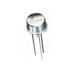
| 描述 | IC VREF SERIES 10V TO5-3参考电压 HI PREC 10V IC REF |
| 产品分类 | |
| 品牌 | Analog Devices |
| 产品手册 | |
| 产品图片 |
|
| rohs | 符合RoHS无铅 / 符合限制有害物质指令(RoHS)规范要求 |
| 产品系列 | 电源管理 IC,参考电压,Analog Devices AD581SH- |
| 数据手册 | |
| 产品型号 | AD581SH |
| 产品种类 | 参考电压 |
| 供应商器件封装 | TO-5-3 |
| 分流电流—最大值 | 10 mA |
| 初始准确度 | 30 mV |
| 包装 | 散装 |
| 参考类型 | Series Precision References |
| 商标 | Analog Devices |
| 安装类型 | 通孔 |
| 容差 | ±0.3% |
| 封装 | Bulk |
| 封装/外壳 | TO-205AA,TO-5-3 金属罐 |
| 封装/箱体 | TO-5-3 |
| 工作温度 | -55°C ~ 125°C |
| 工厂包装数量 | 100 |
| 平均温度系数—典型值 | 30 PPM/C |
| 最大工作温度 | + 125 C |
| 最小工作温度 | - 55 C |
| 标准包装 | 1 |
| 温度系数 | 30ppm/°C |
| 电压-输入 | 12 V ~ 30 V |
| 电压-输出 | 10V |
| 电流-输出 | 10mA |
| 电流-阴极 | - |
| 电流-静态 | 1mA |
| 系列 | AD581 |
| 输入电压 | 40 V |
| 输出电压 | 10 V |
| 通道数 | 1 |


- 商务部:美国ITC正式对集成电路等产品启动337调查
- 曝三星4nm工艺存在良率问题 高通将骁龙8 Gen1或转产台积电
- 太阳诱电将投资9.5亿元在常州建新厂生产MLCC 预计2023年完工
- 英特尔发布欧洲新工厂建设计划 深化IDM 2.0 战略
- 台积电先进制程称霸业界 有大客户加持明年业绩稳了
- 达到5530亿美元!SIA预计今年全球半导体销售额将创下新高
- 英特尔拟将自动驾驶子公司Mobileye上市 估值或超500亿美元
- 三星加码芯片和SET,合并消费电子和移动部门,撤换高东真等 CEO
- 三星电子宣布重大人事变动 还合并消费电子和移动部门
- 海关总署:前11个月进口集成电路产品价值2.52万亿元 增长14.8%


PDF Datasheet 数据手册内容提取
High Precision 10 V IC Reference AD581 FEATURES FUNCTIONAL BLOCK DIAGRAM Laser trimmed to high accuracy 10.000 V ±5 mV (L and U models) +VS Trimmed temperature coefficient 5 ppm/°C maximum, 0°C to 70°C (L model) 10 ppm/°C maximum, −55°C to +125°C (U model) VOUT AD581 Excellent long-term stability 25 ppm/1000 hrs (noncumulative) GND −10 V reference capability L1o0w m qAu ciuesrrceenntt ocuurtrpeuntt c: a1p.0a bmilAit my aximum BOTTTOOM-5 VIEW 08014-001 Figure 1. 3-pin TO-5 package MIL-STD-883 compliant versions available GENERAL DESCRIPTION The AD581J, AD581K, and AD581L are specified for operation The AD581 is a 3-pin, temperature compensated, monolithic, from 0°C to 70°C; the AD581S, AD581T, and AD581U are band gap voltage reference that provides a precise 10.00 V output specified for the −55°C to +125°C range. All grades are from an unregulated input level ranging from 12 V to 30 V. packaged in a hermetically sealed 3-pin TO-5 metal can. Laser wafer trimming (LWT) is used to trim both the initial error at +25°C as well as the temperature coefficient, resulting PRODUCT HIGHLIGHTS in high precision performance previously available only in expen- 1. Laser trimming of both initial accuracy and temperature sive hybrids or oven regulated modules. The 5 mV initial error coefficient results in very low errors over temperature tolerance and 5 ppm/°C guaranteed temperature coefficient of without the use of external components. The AD581L has the AD581L is available in a monolithic voltage reference. a maximum deviation from 10.000 V of ±7.25 mV from The band gap circuit design used in the AD581 offers several 0°C to 70°C, whereas the AD581U guarantees ±15 mV advantages over classical Zener breakdown diode techniques. maximum total error without external trims from −55°C Most important, no external components are required to to +125°C. achieve full accuracy and significant stability to low power 2. Because the laser trimming is done on the wafer prior to systems. In addition, total supply current to the device, separation into individual chips, the AD581 is extremely including the output buffer amplifier (which can supply up valuable to hybrid designers for its ease of use, lack of to 10 mA) is typically 750 μA. The long-term stability of the required external trims, and inherent high performance. band gap design is equivalent to selected Zener reference 3. The AD581 can also be operated in a 2-pin Zener mode to diodes. provide a precision −10 V reference with just one external resistor to the unregulated supply. The performance in this The AD581 is recommended for use as a reference for 8-, 10- mode is nearly equal to that of the standard 3-pin confi- or 12-bit digital-to-analog converters (DACs) that require an guration. external precision reference. The device is also ideal for all types 4. Advanced circuit design using the band gap concept allows of analog-to-digital converters (ADCs) up to 14-bit accuracy, the AD581 to give full performance with an unregulated either successive approximation or integrating designs, and can input voltage down to 13 V. With an external resistor, the generally offer better performance than that provided by standard device operates with a supply as low as 11.4 V. self-contained references. 5. The AD581 is available in versions compliant with MILSTD-883. Refer to the military datasheet for detailed specifications. Rev. C Information furnished by Analog Devices is believed to be accurate and reliable. However, no responsibility is assumed by Analog Devices for its use, nor for any infringements of patents or other One Technology Way, P.O. Box 9106, Norwood, MA 02062-9106, U.S.A. rights of third parties that may result from its use. Specifications subject to change without notice. No license is granted by implication or otherwise under any patent or patent rights of Analog Devices. Tel: 781.329.4700 www.analog.com Trademarks and registered trademarks are the property of their respective owners. Fax: 781.461.3113 ©2009 Analog Devices, Inc. All rights reserved.
AD581 TABLE OF CONTENTS Features .............................................................................................. 1 Output Current Characteristics ...................................................7 Functional Block Diagram .............................................................. 1 Dynamic Performance ..................................................................7 General Description ......................................................................... 1 Precision High Current Supply ...................................................8 Product Highlights ........................................................................... 1 Connection for Reduced Primary Supply ..................................8 Revision History ............................................................................... 2 The AD581 as a Current Limiter .....................................................9 Specifications ..................................................................................... 3 Negative 10 V Reference ...............................................................9 Absolute Maximum Ratings ............................................................ 5 10 V Reference with Multiplying CMOS DACs or ADCs .......9 ESD Caution .................................................................................. 5 Precision 12-Bit DAC Reference .................................................9 Applying the AD581 ......................................................................... 6 Outline Dimensions ........................................................................ 11 Voltage Variation vs. Temperature ............................................. 6 Ordering Guide ........................................................................... 11 REVISION HISTORY 4/09—Rev. B to Rev. C Updated Format .................................................................. Universal Changes to Table 1 ............................................................................ 3 Changes to Figure 2 .......................................................................... 6 Changes to Figure 11 ........................................................................ 8 Changes to 10 V Reference with Multiplying CMOS DACs or ADCs Section ............................................................................... 9 Changes to Precision 12-Bit DAC Reference Section .................. 9 Changes to Figure 13 ........................................................................ 9 Changes to Figure 15 and Figure 16 ............................................. 10 Updated Outline Dimensions ....................................................... 11 Changes to Ordering Guide .......................................................... 11 Rev. C | Page 2 of 12
AD581 SPECIFICATIONS @ V = +15 V and T = +25°C. IN A Specifications shown in boldface are tested on all production units at final electrical test. Results from those tests are used to calculate outgoing quality levels. All minimum and maximum specifications are guaranteed, although only those shown in boldface are tested on all production units. Table 1. AD581J AD581K AD581L Model Min Typ Max Min Typ Max Min Typ Max Units OUTPUT VOLTAGE TOLERANCE (Error from Nominal 10,000 V Output) ±30 ±10 ±5 mV OUTPUT VOLTAGE CHANGE Maximum Deviation from +25°C ±13.5 ±6.75 ±2.25 mV Value, T to T MIN MAX Temperature Coefficient 30 15 5 ppm/°C LINE REGULATION 15 V ≤ VIN ≤ 30 V 3.0 3.0 3.0 mV (0.002) (0.002) (0.002) %/V 13 V ≤ VIN ≤ 15 V 1.0 1.0 1.0 mV (0.005) (0.005) (0.005) %/V LOAD REGULATION 0 ≤ IOUT ≤ 5 mA 200 500 200 500 200 500 μV/mA QUIESCENT CURRENT 0.75 1.0 0.75 1.0 0.75 1.0 mA TURN-ON SETTLING TIME TO 0.1%1 200 200 200 μs NOISE (0.1 Hz TO 10 Hz) 40 40 40 μV (p-p) LONG-TERM STABILITY 25 25 25 ppm/1000 hr SHORT-CIRCUIT CURRENT 30 30 30 mA OUTPUT CURRENT Source @ +25°C 10 10 10 mA Source T to T 5 5 5 mA MIN MAX Sink T to T 5 5 5 μA MIN MAX TEMPERATURE RANGE Specified 0 70 0 70 0 70 °C Operating −65 +150 −65 +150 −65 +150 °C PACKAGE OPTION2 TO-5 (H-03B) AD581JH AD581KH AD581LH 1 See Figure 7. 2 H indicates the hermetic metal can. Rev. C | Page 3 of 12
AD581 Table 2. AD581S AD581T AD581U Model Min Typ Max Min Typ Max Min Typ Max Units OUTPUT VOLTAGE TOLERANCE (Error from Nominal 10,000 V Output) ±30 ±10 ±5 mV OUTPUT VOLTAGE CHANGE Maximum Deviation from +25°C ±30 ±15 ±10 mV Value, T to T MIN MAX Temperature Coefficient 30 15 10 ppm/°C LINE REGULATION 15 V ≤ VIN ≤ 30 V 3.0 3.0 3.0 mV (0.002) (0.002) (0.002) %/V 13 V ≤ VIN ≤ 15 V 1.0 1.0 1.0 mV (0.005) (0.005) (0.005) %/V LOAD REGULATION 0 ≤ IOUT ≤ 5 mA 200 500 200 500 200 500 μV/mA QUIESCENT CURRENT 0.75 1.0 0.75 1.0 0.75 1.0 mA TURN-ON SETTLING TIME TO 0.1%1 200 200 200 μs NOISE (0.1 Hz TO 10 Hz) 40 40 40 μV (p-p) LONG-TERM STABILITY 25 25 25 ppm/1000 hr SHORT-CIRCUIT CURRENT 30 30 30 mA OUTPUT CURRENT Source @ +25°C 10 10 10 mA Source T to T 5 5 5 mA MIN MAX Sink T to T 200 200 200 μA MIN MAX Sink −55°C to +85°C 5 5 5 mA TEMPERATURE RANGE Specified −55 +125 −55 +125 −55 +125 °C Operating −65 +150 −65 +150 −65 +150 °C PACKAGE OPTION2 TO-5 (H-03B) AD581SH AD581TH AD581UH 1 See Figure 7. 2 H indicates hermetic metal can. Rev. C | Page 4 of 12
AD581 ABSOLUTE MAXIMUM RATINGS Stresses above those listed under Absolute Maximum Ratings Table 3. may cause permanent damage to the device. This is a stress Parameter Rating rating only; functional operation of the device at these or any Input Voltage 40 V other conditions above those indicated in the operational Power Dissipation @ +25°C 600 mW section of this specification is not implied. Exposure to absolute Operating Junction Temperature Range −55°C to +150°C maximum rating conditions for extended periods may affect Lead Temperature (Soldering 10 sec) +300°C device reliability. Thermal Resistance Junction-to-Ambient 150°C/W ESD CAUTION Rev. C | Page 5 of 12
AD581 APPLYING THE AD581 The AD581 is easy to use in virtually all precision reference V+ applications. The three pins are simply: primary supply, ground, R40 R41 and output, with the case grounded. No external components Q20 Q7 Q8 are required even for high precision applications; the degree of Q10 Q11 C52 desired absolute accuracy is achieved simply by selecting the C51 Q12 Q15 R42 required device grade. The AD581 requires less than 1 mA quies- Q6 Q14 10V R34 cent current from an operating supply range of 13 V to 30 V. 13V TO 30V Q16 Q13 R37 Q5 C50 +VS R33 R32 R35 AD581 VOUT 10V Q3 Q4 GND Q2 Q1 08014-002 R39 R30 R36 An external finFeig turriem 2 .m Pina yC obnef idguesrairtieodn t(Boo stteotm th Veie owu) tput level to R31 V– 08014-004 Figure 4. Simplified Schematic exactly 10.000 V within less than a millivolt (calibrated to a main system reference). System calibration may also require a VOLTAGE VARIATION vs. TEMPERATURE reference slightly different from 10.00 V. In either case, the Some confusion exists in the area of defining and specifying optional trim circuit shown in Figure 3 can offset the output by reference voltage error over temperature. Historically, references up to ±30 mV (with the 22 Ω resistor), if needed, with minimal have been characterized using a maximum deviation per degree effect on other device characteristics. Celsius; that is, 10 ppm/°C. However, because of nonlinearities +15V in temperature characteristics, which originated in standard Zener references (such as S-type characteristics) manufacturers TRIM MAX R RANGE Δ TCR opt for the maximum limit error band approach to specify devices. 22Ω ±30mV 3.5ppm/°C This technique involves measurement of the output at three, 12Ω ±10mV 2.0ppm/°C +VS 3.9Ω ±5mV 0.6ppm/°C five, or more different temperatures to guarantee that the output AD581 VOUT +10V voltage falls within the given error band. The temperature charac- 6.8kΩ teristic of the AD581 consistently follows the S-curve shown in GND Figure 5. Three-point measurement of each device guarantees the error band over the specified temperature range. 10kΩ R 10.005 –15V 4.3kΩ 08014-003 Figure 3. Optional Fine Trim Configuration V) (UT 10.000 O V 9.995 08014-005 –55–50–40–30–20–10 0 10 20 30 40 50 60 70 80 90 100110120125 TEMPERATURE (°C) Figure 5. Typical Temperature Characteristic Rev. C | Page 6 of 12
AD581 The error band which is guaranteed with the AD581 is the 12V maximum deviation from the initial value at +25°C; this error 10.03V T band is of more use to a designer than one which simply guarantees TPU 11V 10.02V UT U P the maximum total change over the entire range (that is, in the O T 10.01V U O latter definition, all of the changes could occur in the positive 10V 10.00V direction). Thus, with a given grade of the AD581, the designer 20V can easily determine the maximum total error from initial toler- T ance plus temperature variation (for example, for the AD581T, the PU 10V N I itnhiutisa tl htoel eurnaint cies igsu ±a1r0a nmteVe,d t htoe tbeem 1p0e.r0a0tu0r Ve e±rr2o5r mbaVn dfr ios m±1 −55 m5°VC, 0V 08014-007 0 50 100 150 200 250 to +125°C). SETTLING TIME (µs) OUTPUT CURRENT CHARACTERISTICS Figure 7. Output Settling Characteristic The AD581 has the capability to either source or sink current and provide good load regulation in either direction, although 1000 it has better characteristics in the source mode (positive current NOISE SPECTRAL DENSITY (nV/ Hz) into the load). The circuit is protected for shorts to either positive supply or ground. The output voltage vs. output current charac- 100 teristics of the device are shown in Figure 6. Source current is displayed as negative current in the figure; sink current is positive. Note that the short-circuit current (that is, 0 V output) TOTAL NOISE (µV rms) UP is about 28 mA; when shorted to +15 V, the sink current goes to TO SPECIFIED FREQUENCY 10 about 20 mA. 14 T+VA S= =2 51°5CV 1 08014-008 12 10 100 1k 10k 100k 1M GE (V)10 Figure 8. Spectral Noise DeFnRsiEtQy UaEnNdC TYo (tHazl )rms Noise vs. Frequency A T L O 8 V T U 1000 P 6 T U O 4 900 20 –20 –15 –10 –5 0 5 10 15 20 08014-006 RENT (µA) 800 1.5µA/°C SOURCE SINK R U Figure 6. Output OVoUlTtPaUgTe vCsU. RSRinEkN aTn (md AS)ource Current PLY C 700 P U DYNAMIC PERFORMANCE S 600 Mcreaansyi nlogwly pcoonwceerr innesdtr wumithe ntht em taunrnuf-aocnt ucrhearrsa hctaevrei sbtiecesn o ifn t-he 500 08014-009 components used in their systems. Fast turn-on components often –55–50–40–30–20–10 0 10 20 30 40 50 60 70 80 90 100110120125 TEMPERATURE (°C) enable the end user to keep power off when not needed, and yet Figure 9. Quiescent Current vs. Temperature respond quickly when the power is turned on for operation. Figure 7 displays the turn-on characteristic of the AD581. This characteristic is generated from a cold start operation and repre- sents the true turn-on waveform after an extended period with the supplies off. The figure shows both the coarse and fine transient characteristics of the device; the total settling time to within ±10 mV is about 180 μs, and there is no long thermal tail appearing after the point. Rev. C | Page 7 of 12
AD581 PRECISION HIGH CURRENT SUPPLY CONNECTION FOR REDUCED PRIMARY SUPPLY The AD581 can be easily connected with power pnp or power Whereas line regulation is specified down to 13 V, the typical Darlington pnp devices to provide much greater output current AD581 works as specified ≤12 V. The current sink capability capability. The circuit shown in Figure 10 delivers a precision allows even lower supply voltage capability such as operation 10 V output with up to 4 A supplied to the load. The 0.1 μF from 12 V ±5% as shown in Figure 11. The 560 Ω resistor reduces capacitor is required only if the load has a significant capacitive the current supplied by the AD581 to a manageable level at a component. If the load is purely resistive, improved high frequency full 5 mA load. Note that the other band gap references, without supply rejection results from removing the capacitor. current sink capability, may be damaged by use in this circuit VIN ≥ 15V configuration. 12V ±5% 470Ω +VS 560Ω 5% AD581 10V @ 0mA TO 5mA VOUT 2N6040 GND 08014-011 Figure 11. 12 V Supply Connection 0.1µF +VS AD581 VOUT VOUT 10V @ 4A GND 08014-010 Figure 10. High Current Precision Supply Rev. C | Page 8 of 12
AD581 THE AD581 AS A CURRENT LIMITER The AD581 represents an alternative to current limiter diodes ANALOG GND that require factory selection to achieve a desired current. This +VS approach often results in temperature coefficients of 1%/°C. 0.1µF AD581 The AD581 approach is not limited to a defined set current VOUT limit; it can be programmed from 0.75 mA to 5 mA with the GND VREF insertion of a single external resistor. Of course, the minimum –10V voltage required to drive the connection is 13 V. The AD580, 1.2kΩ 5% which is a 2.5 V reference, can be used in this type of circuit –15V 08014-013 with compliance voltage down to 4.5 V. Figure 13. 2-Pin −10 V Reference 10 V REFERENCE WITH MULTIPLYING CMOS DACs OR ADCs +VS AD581 10V = i ~= 1_0_V_ + 0.75mA The AD581 is ideal for application with the entire AD7533 VOUT R series of 10- and 12-bit multiplying CMOS DACs, especially for GND R LOAD low power applications. It is equally suitable for the AD7574 8-bit ADC. In the standard hook-up, as shown in Figure 15, the +10 V reference is inverted by the amplifier/DAC configuration BOTTOM VIEW OF 1RIN0E VTF OEPRR-5EE CNCACISSEIEO CNIRCUIT 08014-012 ttoot parl oqduuiecsec ean 0t sVu ptop l−y 1c0u rVre rnatn isg ety. pIfic aanll yO 2P m11A7.7 I fa am 0p Vlif tioer + i1s 0u Vse d, Figure 12. A Two-Component Precision Current Limiter full-scale range is desired, the AD581 can be connected to the NEGATIVE 10 V REFERENCE CMOS DAC in its −10 V Zener mode, as shown in Figure 13 (the −10 V output is connected directly to the V of the REF REF IN The AD581 can also be used in a 2-pin Zener mode to provide a CMOS DAC). The AD581 is normally used in the −10 V mode precision −10.00 V reference. As shown in Figure 13, the +V and S with the AD7574 to give a 0 V to +10 V ADC range. This is V pins are connected together to the high supply (in this OUT shown in Figure 15. Bipolar output applications and other case, ground). The ground pin is connected through a resistor operating details can be found in the data sheets for the CMOS to the negative supply. Thus, the output is taken from the products. ground pin instead of V . With 1 mA flowing through the OUT +15V AD581 in this mode, a typical unit shows a 2 mV increase in output level over that produced in the 3-pin mode. Note also +10V that the effective output impedance in this connection increases AD581 from 0.2 Ω typical to 2 Ω. It is essential to arrange the output VREF IN load and the supply resistor, R, so that the net current through S BIT 1 (MSB) 15 14 RFEEDBACK the AD581 is always between 1 mA and 5 mA. For operation to 4 16 +125°C, the net current should be between 2 mA and 5 mA. The DIIGNIPTUATL 5 IOUT1 +15V 1 temperature characteristics and long-term stability of the device VOUT 0V TO –10V are essentially the same as that of a unit used in the standard IOUT2 3-pin mode. 13 2 –15V The AD581 can also be used in a 2-pin mode to develop a BIT 10 (LSB) 3GND 08014-014 positive reference. +VS and VOUT are tied together and to the Figure 14. Low Power 10-Bit CMOS DAC Application positive supply through an appropriate supply resistor. The PRECISION 12-BIT DAC REFERENCE performance characteristics are similar to those of the negative 2-pin connection. The only advantage of this connection over AD565A, like most DACs, is designed to operate with a +10 V the standard 3-pin connection is that a lower primary supply reference element. In the AD565A, this 10 V reference voltage is can be used, as low as 10.5 V. This type of operation requires con- converted into a reference current of approximately 0.5 mA via siderable attention to load and primary supply regulation to the internal 19.95 kΩ resistor (in series with the external 100 Ω maintain the AD581 within its regulating range of 1 mA to 5 mA trimmer). The gain temperature coefficient of the AD565A is (2 mA to 5 mA for operation beyond +85°C). primarily governed by the temperature tracking of the 19.95 kΩ resistor and the 5 kΩ to10 kΩ span resistors; gain TC is guaran- teed to 3 ppm/°C. Thus, using the AD581L (at 5 ppm/°C) as the Rev. C | Page 9 of 12
AD581 10 V reference guarantees a maximum full-scale temperature –15V +5V coefficient of 8 ppm/°C over the commercial range. The 10 V R3 AD581 1.2kΩ GAIN TRIM1 1 AD7574 18 reference also supplies the normal 1 mA bipolar offset current GND 5% R2 2kΩ (TOP VIEW) 2 through the 9.95 kΩ bipolar offset resistor. Consequently, the +VS VOUT –10V REFR1 1kΩ 10%1 3 DSUIGPIPTLAYL bipolar offset TC depends only on TC matching of the bipolar SIGNAL 4 RETURN 0.1µF INPUT offset resistor to the input reference resistor and is guaranteed 0V TO +10V 5 to 3 ppm/°C. ASNUAPLPOLGY IGNRTOERUTNIDE RETURN ANALOG GROUND 1RIS1 NAONTD RRE2Q CUAIRNE BDE. OMITTED IF GAIN TRIM 08014-015 Figure 15. AD581 as −10 V Reference for CMOS ADC –15V +5V/+15V 24 23 22 21 20 19 18 17 16 15 14 13 0.1µF 6 1 2 +15V 0.1µF BIT 1(MSB) BIT 2 BIT 3 BIT 4 BIT 5 BIT 6 BIT 7 BIT 8 BIT 9 BIT 10 BIT 11 BIT 12(LSB)(85kkΩΩ) 11 10 CONTROL AMP 0.5mA PNP LOGIC SWITCHES AND LEVEL SHIFTERS (85kkΩΩ) 2 SUMMING 4 9 +VS JUNCTION OP1177 GAIN ADJ. CONTROL 12 3 OP AMP 10V 5 19.95kΩ AMP OUTPUT AD581 VOUT 100Ω, 15T A R2 AD565A R3 +15V GND 8 3.0MΩ R4 20kΩ, 15T 3 9.950kΩ –15V (15.95k) 7 UNIPOLAR A OFFSET ADJ. –15V R1 1B0IP0ΩO,L 1A5RT OFFSET ADJ. A = ANALOG GROUND 08014-016 Figure 16. Precision 12-Bit DAC Rev. C | Page 10 of 12
AD581 OUTLINE DIMENSIONS 0.185 (4.70) 0.165 (4.19) 0.500 (12.70) MIN 0.100 (2.54) TYP 0)1) 1)5) 3 0.045 (1.14) 370 (9.4335 (8.5 335 (8.5305 (7.7 (05.T.20Y08P0) 2 00.0.02394 ( (00.7.846)) 0.0. 0.0. 0.019 (0.48) 1 0.028 (0.71) 0.016 (0.41) 0.030 (0.76) MAX 45° BASE & SEATING PLANE C(RINOE FNPETARRREOENLNCLTEIHN EOGSN DELISYM) EAANNRSDEI OARNROSEU ANNRDOEET D IAN-OP IPFNRFC OHINPECRSHI;A METQIEL ULFIIOVMAREL TUEESNRET DSINI MF DOEENRSSIGIONN.S 030309-A Figure 17. 3-Pin Metal Header Package [TO-5] (H-03B) Dimensions shown in inches and (millimeters) ORDERING GUIDE Model Temperature Range Package Description Package Option AD581JH1 0°C to +70°C 3-Pin Metal Header Package (TO-5) H-03B AD581KH1 0°C to +70°C 3-Pin Metal Header Package (TO-5) H-03B AD581LH1 0°C to +70°C 3-Pin Metal Header Package (TO-5) H-03B AD581SH1 −55°C to +125°C 3-Pin Metal Header Package (TO-5) H-03B AD581TH1 −55°C to +125°C 3-Pin Metal Header Package (TO-5) H-03B AD581UH1 −55°C to +125°C 3-Pin Metal Header Package (TO-5) H-03B 1 RoHS compliant model as of Date Code 0713. Rev. C | Page 11 of 12
AD581 NOTES ©2009 Analog Devices, Inc. All rights reserved. Trademarks and registered trademarks are the property of their respective owners. D08014-0-4/09(C) Rev. C | Page 12 of 12
Mouser Electronics Authorized Distributor Click to View Pricing, Inventory, Delivery & Lifecycle Information: A nalog Devices Inc.: 5962-8688203XA AD581KH AD581TH/883B AD581UH AD581SH/883B AD581UH/883B AD581SH AD581JH AD581LH AD581TH