ICGOO在线商城 > 集成电路(IC) > PMIC - 电压基准 > NCP431ACLPRAG
 Datasheet下载
- 型号: NCP431ACLPRAG
- 制造商: ON Semiconductor
- 库位|库存: xxxx|xxxx
- 要求:
| 数量阶梯 | 香港交货 | 国内含税 |
| +xxxx | $xxxx | ¥xxxx |
查看当月历史价格
查看今年历史价格
NCP431ACLPRAG产品简介:
ICGOO电子元器件商城为您提供NCP431ACLPRAG由ON Semiconductor设计生产,在icgoo商城现货销售,并且可以通过原厂、代理商等渠道进行代购。 NCP431ACLPRAG价格参考。ON SemiconductorNCP431ACLPRAG封装/规格:PMIC - 电压基准, 分流器 电压基准 IC 36V ±1% 100mA TO-92。您可以下载NCP431ACLPRAG参考资料、Datasheet数据手册功能说明书,资料中有NCP431ACLPRAG 详细功能的应用电路图电压和使用方法及教程。
NCP431ACLPRAG是ON Semiconductor(现为安森美半导体)生产的一款精密可调分流稳压器,属于PMIC(电源管理集成电路)中的电压基准类别。它具有高精度、低功耗和小封装等特点,广泛应用于需要精确电压参考的各种电路中。

 应用场景

1. 电源管理
   - NCP431ACLPRAG常用于电源管理系统中,作为电压基准源。它可以提供稳定的参考电压,确保电源输出的稳定性。例如,在开关电源、线性稳压器等设计中,该器件可以用来设定输出电压或作为反馈网络的一部分。

2. 数据采集系统
   - 在数据采集系统中,NCP431ACLPRAG可以用作ADC(模数转换器)的参考电压源。由于其高精度和低温度漂移特性,能够显著提高ADC的测量精度,适用于工业控制、医疗设备等领域。

3. 电池管理
   - 该器件也适用于电池管理系统(BMS),帮助监测电池电压状态,确保电池充电和放电过程的安全性和效率。通过提供稳定的参考电压,NCP431ACLPRAG有助于实现更精确的电量估算和保护功能。

4. 通信设备
   - 在通信设备中,如基站、路由器等,NCP431ACLPRAG可以用于生成稳定的参考电压,以确保信号处理和传输的准确性。其低噪声特性有助于减少干扰,提升通信质量。

5. 消费电子
   - 消费电子产品如智能手机、平板电脑等,也需要精确的电压基准来保证各种传感器、显示屏和其他组件的正常工作。NCP431ACLPRAG的小尺寸和高效能使其成为这些应用的理想选择。

6. 汽车电子
   - 在汽车电子领域,如车载信息娱乐系统、发动机控制单元(ECU)等,NCP431ACLPRAG可以提供稳定可靠的电压基准,确保系统的稳定运行,尤其是在严苛的工作环境下。

总之,NCP431ACLPRAG凭借其高精度、低功耗和紧凑的设计,适用于多种需要精确电压参考的应用场合,特别是在对性能和可靠性要求较高的行业中表现尤为突出。
| 参数 | 数值 |
| 产品目录 | 集成电路 (IC)半导体 |
| 描述 | IC VREF SHUNT PREC ADJ参考电压 ANA 2.5V PROG SHUNT REF |
| 产品分类 | |
| 品牌 | ON Semiconductor |
| 产品手册 | |
| 产品图片 |
|
| rohs | 符合RoHS无铅 / 符合限制有害物质指令(RoHS)规范要求 |
| 产品系列 | 电源管理 IC,参考电压,ON Semiconductor NCP431ACLPRAG- |
| 数据手册 | |
| 产品型号 | NCP431ACLPRAG |
| 串联VREF—电源电流—最大值 | 10 mA |
| 串联VREF—输入电压—最大值 | 2.525 V |
| 串联VREF—输入电压—最小值 | 2.475 V |
| 产品种类 | 参考电压 |
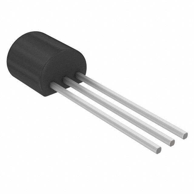
| 供应商器件封装 | TO-92 |
| 其它名称 | NCP431ACLPRAGOSTR |
| 分流电流—最大值 | 100 mA |
| 分流电流—最小值 | 40 uA |
| 初始准确度 | 1 % |
| 包装 | 带卷 (TR) |
| 参考类型 | Shunt Adjustable Precision References |
| 商标 | ON Semiconductor |
| 安装类型 | 通孔 |
| 安装风格 | Through Hole |
| 容差 | ±1% |
| 封装 | Reel |
| 封装/外壳 | TO-226-3、TO-92-3 标准主体 |
| 封装/箱体 | TO-92 |
| 工作温度 | 0°C ~ 70°C |
| 工厂包装数量 | 2000 |
| 平均温度系数—典型值 | 50 PPM / C |
| 最大工作温度 | + 70 C |
| 最小工作温度 | 0 C |
| 标准包装 | 2,000 |
| 温度系数 | 标准值 50ppm/°C |
| 电压-输入 | - |
| 电压-输出 | 2.4 V ~ 36 V |
| 电流-输出 | 100mA |
| 电流-阴极 | 80µA |
| 电流-静态 | - |
| 系列 | NCP431 |
| 输入电压 | 2.5 V |
| 输出电压 | 36 V |
| 通道数 | 1 |


- 商务部:美国ITC正式对集成电路等产品启动337调查
- 曝三星4nm工艺存在良率问题 高通将骁龙8 Gen1或转产台积电
- 太阳诱电将投资9.5亿元在常州建新厂生产MLCC 预计2023年完工
- 英特尔发布欧洲新工厂建设计划 深化IDM 2.0 战略
- 台积电先进制程称霸业界 有大客户加持明年业绩稳了
- 达到5530亿美元!SIA预计今年全球半导体销售额将创下新高
- 英特尔拟将自动驾驶子公司Mobileye上市 估值或超500亿美元
- 三星加码芯片和SET,合并消费电子和移动部门,撤换高东真等 CEO
- 三星电子宣布重大人事变动 还合并消费电子和移动部门
- 海关总署:前11个月进口集成电路产品价值2.52万亿元 增长14.8%


PDF Datasheet 数据手册内容提取
NCP431A, SC431A, NCP431B, SC431B, NCP432B, SC432B Series Programmable Precision References The NCP431/NCP432 integrated circuits are three−terminal www.onsemi.com programmable shunt regulator diodes. These monolithic IC voltage references operate as a low temperature coefficient zener which is programmable from Vref to 36 V using two external resistors. These devices exhibit a wide operating current range of 40 (cid:2)A to 100 mA with a typical dynamic impedance of 0.22 (cid:3). The characteristics of Pin 1. Reference these references make them excellent replacements for zener diodes in 2. Anode many applications such as digital voltmeters, power supplies, and op 12 3. Cathode 1 2 amp circuitry. The 2.5 V reference makes it convenient to obtain a 3 3 stable reference from 5.0 V logic supplies, and since the NCP431/ STRAIGHT LEAD BENT LEAD BULK PACK TAPE & REEL NCP432 operates as a shunt regulator, it can be used as either a AMMO PACK positive or negative voltage reference. Low minimum operating current makes this device an ideal choice for secondary regulators in TO−92 TO−92 LP SUFFIX LPRA SUFFIX SMPS adapters with extremely low no−load consumption. CASE 29−11 CASE 29−11 Features • Programmable Output Voltage to 36 V SOIC−8 NB • Low Minimum Operating Current: 40 (cid:2)A, Typ @ 25°C 8 D SUFFIX • Voltage Reference Tolerance: ±0.5%, Typ @ 25°C 1 CASE 751 (NCP431B/NCP432B) • Low Dynamic Output Impedance, 0.22 (cid:3) Typical Cathode 1 Reference • Sink Current Capability of 40 (cid:2)A to 100 mA Anode Anode • Equivalent Full−Range Temperature Coefficient of 50 ppm/°C Anode Anode NC NC Typical • (Top View) Temperature Compensated for Operation over Full Rated Operating Temperature Range 3 • SOT−23 SC Prefix for Automotive and Other Applications Requiring Unique SN SUFFIX Site and Control Change Requirements; AEC−Q100 Qualified and 1 CASE 318 PPAP Capable 2 • These are Pb−Free Devices NCP431/SC431 NCP432/SC432 Pin 1. Reference Pin 1. Cathode Typical Applications 2. Cathode 2. Reference • Voltage Adapters 3. Anode 3. Anode • Switching Power Supply • Precision Voltage Reference • ORDERING AND MARKING INFORMATION Charger • See detailed ordering and shipping information in the package Instrumentation dimensions section on page 14 of this data sheet. © Semiconductor Components Industries, LLC, 2011 1 Publication Order Number: January, 2019 − Rev. 16 NCP431/D
NCP431A, SC431A, NCP431B, SC431B, NCP432B, SC432B Series Cathode Reference Cathode (R) (K) (K) 2.5V ref Reference (R) Anode Anode (A) (A) Figure 1. Symbol Figure 2. Representative Block diagram This device contains 20 active transistors MAXIMUM RATINGS (Full operating ambient temperature range applies, unless otherwise noted) Symbol Rating Value Unit VKA Cathode to Anode Voltage 37 V IK Cathode Current Range, Continuous −100 to +150 mA Iref Reference Input Current Range, Continuous −5 to +10 mA TJ Operating Junction Temperature 150 °C TA Operating Ambient Temperature Range −40 to +125 °C Tstg Storage Temperature Range −65 to +150 °C PD Total Power Dissipation @ TA = 25°C W Derate above 25°C Ambient Temperature D, LP Suffix Plastic Package 0.70 SN1 Suffix Plastic Package 0.52 PD Total Power Dissipation @ TC = 25°C 1.5 W Derate above 25°C Case Temperature D, LP Suffix Plastic Package ESD Rating (Note 1) V HBM Human Body Model per JEDEC JESD22−A114F >2000 CDM Charged Device Model per JEDEC JESD22−C101E >1000 Stresses exceeding those listed in the Maximum Ratings table may damage the device. If any of these limits are exceeded, device functionality should not be assumed, damage may occur and reliability may be affected. 1. This device contains latch−up protection and exceeds ±100 mA per JEDEC standard JESD78. RECOMMENDED OPERATING CONDITIONS Symbol Condition Min Max Unit VKA Cathode to Anode Voltage Vref 36 V IK Cathode Current 0.04 100 mA Functional operation above the stresses listed in the Recommended Operating Ranges is not implied. Extended exposure to stresses beyond the Recommended Operating Ranges limits may affect device reliability. THERMAL CHARACTERISTICS LP Suffix Package D Suffix Package SN Suffix Package Symbol Characteristic (50 mm2 x 35 (cid:2)m Cu) (50 mm2 x 35 (cid:2)m Cu) (10 mm2 x 35 (cid:2)m Cu) Unit R(cid:4)JA Thermal Resistance, 176 210 255 °C/W Junction−to−Ambient R(cid:4)JL Thermal Resistance, 75 68 80 °C/W Junction−to−Lead (Lead 3) www.onsemi.com 2
NCP431A, SC431A, NCP431B, SC431B, NCP432B, SC432B Series ELECTRICAL CHARACTERISTICS (TA = 25°C, unless otherwise noted.) NCP431AV/ NCP431AC NCP431AI SC431AV Symbol Characteristic Min Typ Max Min Typ Max Min Typ Max Unit Vref Reference Input Voltage V VKA = Vref, IK = 1 mA TA = 25°C 2.475 2.500 2.525 2.475 2.500 2.525 2.475 2.500 2.525 TA = Tlow to Thigh (Figure 3, Note 2) 2.475 2.500 2.525 2.465 2.500 2.525 2.460 2.500 2.525 (cid:5)VrefT Reference Input Voltage Deviation Over Temperat- − − − − 5.0 10 − 10 15 mV ure Range (Figure 3, Notes 3, 4) VKA= Vref, IK = 1 mA (cid:5)Vref Ratio of Change in Reference Input Voltage to mV/ (cid:5)VKA Change in Cathode to Anode Voltage V IK = 1 mA (Figure 4), (cid:5)VKA = 10 V to Vref − −1.85 −3.1 − −1.85 −3.1 − −1.85 −3.1 (cid:5)VKA = 36 V to 10 V − −0.80 −1.8 − −0.80 −1.8 − −0.80 −1.8 Iref Reference Input Current (Figure 4) nA IK = 1 mA, R1 = 220 k, R2 = (cid:2) − 81 190 − 81 190 − 81 190 TA = −40°C to +125°C (cid:5)IrefT Reference Input Current Deviation Over Temperat- nA ure Range (Figure 4, Note 3) − 22 55 − 22 55 − 22 55 IK = 1 mA, R1 = 10 k, R2 = (cid:2) Imin Minimum Cathode Current For Regulation − 40 60 − 40 60 − 40 60 (cid:2)A VKA = Vref (Figure 3) Ioff Off−State Cathode Current (Figure 5) − 180 1000 − 180 1000 − 180 1000 nA VKA = 36 V, Vref = 0 V |ZKA| Dynamic Impedance (Figure 3, Note 5) − 0.22 0.5 − 0.22 0.5 − 0.22 0.5 (cid:3) VKA = Vref, (cid:5)IK = 1.0 mA to 100 mA f (cid:3) 1.0 kHz Product parametric performance is indicated in the Electrical Characteristics for the listed test conditions, unless otherwise noted. Product performance may not be indicated by the Electrical Characteristics if operated under different conditions. 2. Tlow = −40°C for NCP431AI, NCP431AV, SC431AV = 0°C for NCP431AC Thigh = 70°C for NCP431AC = 85°C for NCP431AI = 125°C for NCP431AV, SC431AV 3. Guaranteed by design 4. The deviation parameter (cid:5)VrefT is defined as the difference between the maximum and minimum values obtained over the full operating ambient temperature range that applies. (cid:5) (cid:6) The average temperature coefficient of the reference input voltage, Vref is defined as: (cid:5)Vref (cid:7)106 ppm Vref@25°C (cid:5)Vref(cid:7)106 Vref °C (cid:4) (cid:5)TA (cid:4)(cid:5)T (cid:5)V @25°C(cid:6) A ref (cid:6)Vref can be positive or negative depending on whether Vref Min or Vref Max occurs at the lower ambient temperature. Example:(cid:5)VrefT = 17 mV and slope is positive Vref = 2.5 V, (cid:5)TA = 165°C (from −40°C to +125°C) 0.017(cid:8)106 (cid:6)V (cid:4) (cid:4)41.2ppm(cid:9)°C ref 165(cid:8)2.5 5. The dynamic impedance ZKA is defined as: (|ZKA| = ((cid:5)VKA/(cid:5)IK). When the device is programmed with two external resistors, R1 and R2, the total dynamic impedance of the circuit is defined as: |ZKA’| (cid:10) |ZKA| (1 + (R1/R2)). 6. SC431AVSNT1G − Tlow = −40°C, Thigh = 125°C. Guaranteed by design. SC Prefix for Automotive and Other Applications Requiring Unique Site and Control Change Requirements; AEC−Q100 Qualified and PPAP Capable. www.onsemi.com 3
NCP431A, SC431A, NCP431B, SC431B, NCP432B, SC432B Series ELECTRICAL CHARACTERISTICS (TA = 25°C, unless otherwise noted.) NCP431BC NCP431BI NCP/SC431BV NCP432BC NCP432BI NCP/SC432BV Symbol Characteristic Min Typ Max Min Typ Max Min Typ Max Unit Vref Reference Input Voltage V VKA = Vref, IK = 1 mA TA = 25°C 2.4875 2.500 2.5125 2.4875 2.500 2.5125 2.4875 2.500 2.5125 TA = Tlow to Thigh (Figure 3, Note 7) 2.4875 2.500 2.5125 2.4775 2.500 2.5125 2.4725 2.500 2.5125 (cid:5)VrefT Reference Input Voltage Deviation Over Tem- − − − − 5.0 10 − 10 15 mV perature Range (Figure 3, Notes 8, 9) − − − 1− − 15 VKA= Vref, IK = 1 mA (cid:5)Vref Ratio of Change in Reference Input Voltage to mV/ (cid:5)VKA Change in Cathode to Anode Voltage V IK = 1 mA (Figure 4), (cid:5)VKA = 10 V to Vref − −1.85 −3.1 − −1.85 −3.1 − −1.85 −3.1 (cid:5)VKA = 36 V to 10 V − −0.80 −1.8 − −0.80 −1.8 − −0.80 −1.8 Iref Reference Input Current (Figure 4) nA IK = 1 mA, R1 = 220 k, R2 = (cid:2) − 81 190 − 81 190 − 81 190 TA = −40°C to +125°C (cid:5)IrefT Reference Input Current Deviation Over Tem- nA perature Range (Figure 4, Note 8) − 22 55 − 22 55 − 22 55 IK = 1 mA, R1 = 10 k, R2 = (cid:2) Imin Minimum Cathode Current For Regulation − 40 60 − 40 60 − 40 60 (cid:2)A VKA = Vref (Figure 3) Ioff Off−State Cathode Current (Figure 5) − 180 1000 − 180 1000 − 180 1000 nA VKA = 36 V, Vref = 0 V |ZKA| Dynamic Impedance (Figure 3, Note 10) − 0.22 0.5 − 0.22 0.5 − 0.22 0.5 (cid:3) VKA = Vref, (cid:5)IK = 1.0 mA to 100 mA f (cid:3) 1.0 kHz Product parametric performance is indicated in the Electrical Characteristics for the listed test conditions, unless otherwise noted. Product performance may not be indicated by the Electrical Characteristics if operated under different conditions. 7. Tlow = −40°C for NCP431BI, NCP431BV, NCP432BI, NCP432BV, SC431B, SC432B = 0°C for NCP431BC, NCP432BC Thigh = 70°C for NCP431BC, NCP432BC = 85°C for NCP431BI, NCP432BI = 125°C for NCP431BV, NCP432BV, SC431BV, SC432BV 8. Guaranteed by design 9. The deviation parameter (cid:5)VrefT is defined as the difference between the maximum and minimum values obtained over the full operating ambient temperature range that applies. (cid:5) (cid:6) The average temperature coefficient of the reference input voltage, Vref is defined as: (cid:5)Vref (cid:7)106 ppm Vref@25°C (cid:5)Vref(cid:7)106 Vref °C (cid:4) (cid:5)TA (cid:4)(cid:5)T (cid:5)V @25°C(cid:6) A ref (cid:6)Vref can be positive or negative depending on whether Vref Min or Vref Max occurs at the lower ambient temperature. Example:(cid:5)VrefT = 17 mV and slope is positive Vref = 2.5 V, (cid:5)TA = 165°C (from −40°C to +125°C) 0.017(cid:8)106 (cid:6)V (cid:4) (cid:4)41.2ppm(cid:9)°C ref 165(cid:8)2.5 10.The dynamic impedance ZKA is defined as: (|ZKA| = ((cid:5)VKA/(cid:5)IK). When the device is programmed with two external resistors, R1 and R2, the total dynamic impedance of the circuit is defined as: |ZKA’| (cid:10) |ZKA| (1 + (R1/R2)) 11.SC431BVSNT1G, SC432BVSNT1G − Tlow = −40°C, Thigh = 125°C. Guaranteed by design. SC Prefix for Automotive and Other Applica- tions Requiring Unique Site and Control Change Requirements; AEC−Q100 Qualified and PPAP Capable. www.onsemi.com 4
NCP431A, SC431A, NCP431B, SC431B, NCP432B, SC432B Series Input VKA Input VKA Input VKA IK Ioff R1 Iref IK Vref R2 Vref VKA(cid:4)Vref(cid:5)1(cid:11)RR12(cid:6)(cid:11)Iref(cid:8)R1 Figure 3. Test Circuit for V = V Figure 4. Test Circuit for V > V Figure 5. Test Circuit for I KA ref KA ref off 150.0 60.0 T (mA) 100.0 Input TVAKA= =2 5V°rCefIK VKA (cid:2)T (A) 40.0 Input TVAKA= =2 5V°rCefIK VKA IMin N N E E 20.0 RR 50.0 RR U U C C 0.0 E E D 0.0 D O O H H−20.0 T T A A , CK −50.0 , CK−40.0 I I −100.0 −60.0 −1.0 0.0 1.0 2.0 3.0 −1.0 0.0 1.0 2.0 3.0 VKA, CATHODE VOLTAGE (V) VKA, CATHODE VOLTAGE (V) Figure 6. Cathode Current versus Cathode Figure 7. Cathode Current versus Cathode Voltage Voltage 80.00 70.00 60.00 50.00 A) (cid:2) , (N 40.00 MI I 30.00 20.00 10.00 0.00 −50 −25 0 25 50 75 100 125 TA, AMBIENT TEMPERATURE (°C) Figure 8. Minimum Cathode Current Regulation versus Ambient Temperature www.onsemi.com 5
NCP431A, SC431A, NCP431B, SC431B, NCP432B, SC432B Series V) 2540 A) 120 E (m 2530 Input VKA VIKK =A 1= mVrAef NT (n 110 Input IK = 1 mA VKA G IK E OLTA 2520 URR 100 220k Iref IK T V 2510 Vref T C 90 U U NP 2500 NP 80 E I E I C 2490 C 70 N N E E R 2480 R 60 E E F F RE 2470 RE 50 V, ref 2460 I, ref 40 −50 −25 0 25 50 75 100 125 −50 −25 0 25 50 75 100 125 TA, AMBIENT TEMPERATURE (°C) TA, AMBIENT TEMPERATURE (°C) Figure 9. Reference Input Voltage versus Figure 10. Reference Input Current versus Ambient temperature Ambient temperature GE (mV) 0 Input R1 IK VKA ENT (nA)100 Input VVKrAef==306VVIoff VKA A −10 R T R PUT VOL −20 R2 Vref ODE CU 10 N H E I AT C C N E E −30 T R A E T EF VKA = Vref −S R IK = 1 mA FF (cid:5)V, ref −400 10 20 30 40 I, Ooff 1−50 −25 0 25 50 75 100 125 VKA, CATHODE VOLTAGE (V) TA, AMBIENT TEMPERATURE (°C) Figure 11. Change in Reference Input Voltage Figure 12. Off−State Cathode Current versus versus Cathode Voltage Ambient Temperature 10 0.320 (cid:3)) 1.0k Output (cid:3)) E ( IK E ( 0.300 C 50 C N N DA GND DA 0.280 E E P P M M MIC I 1 MIC I 0.260 (cid:5)IK=1V.0KmA=A Vtoref100mA NA NA 0.240 f<1.0kHz Output DY DY 1.0k IK Z|, KA (cid:5)TAIK = = 2 15 °mCA to 100 mA Z|, KA 0.220 50 GND | | 0.1 0.200 0.001 0.01 0.1 1 10 100 −50 −25 0 25 50 75 100 125 f, FREQUENCY (MHz) TA, AMBIENT TEMPERATURE (°C) Figure 13. Dynamic Impedance versus Figure 14. Dynamic Impedance versus Ambient Frequency Temperature www.onsemi.com 6
NCP431A, SC431A, NCP431B, SC431B, NCP432B, SC432B Series B) 60 800 d GAIN ( 50 9.0(cid:2)F 15k IK 230Output Z) 700 GE 40 8.25k √V/H 600 A GND n OLT 30 GE ( 500 PEN LOOP V 1200 OISE VOLTA 234000000 Input TVIKAK=A==125mV°rACef IK VKA O N , L 0 IK = 100 (cid:2)A to 10 mA 100 VO TA = 25°C A −10 0 10 100 1000 10k 100k 1000 10k 100k 1M 10M f, FREQUENCY (Hz) f, FREQUENCY (Hz) Figure 15. Open−Loop Voltage Gain versus Figure 16. Spectral Noise Density Frequency Input Monitor 4.0 220 Output A) G (V) 32..00 Output fG=eP1nu0el0sraektHorz 50 NT (m N E WI 1.0 GND R R S U E C G E LTA 10 OD O H V 5.0 AT Input C 0 , K I 0 4.0 8.0 12 16 20 24 28 32 36 40 t, TIME ((cid:2)s) CL, LOAD CAPACITANCE (nF) Figure 17. Pulse Response Figure 18. Stability Boundary Conditions Figure 19. Stability Boundary Conditions for Small Cathode Current www.onsemi.com 7
NCP431A, SC431A, NCP431B, SC431B, NCP432B, SC432B Series 150 150 VOUT VOUT IK IK 10k V+ CL V+ CL Figure 20. Test Circuit For Curve A of Stability Figure 21. Test Circuit For Curve B And C of Boundary Conditions Stability Boundary Conditions www.onsemi.com 8
NCP431A, SC431A, NCP431B, SC431B, NCP432B, SC432B Series TYPICAL APPLICATIONS V+ VOUT V+ VOUT R1 IK R1 CL R2 R2 (cid:5) (cid:6) VOUT(cid:4) 1(cid:11)RR12 Vref (cid:5) (cid:6) VOUT(cid:4) 1(cid:11)RR12 Vref Figure 22. Shunt Regulator Figure 23. High Current Shunt Regulator V+ VOUT MC7805 V+ In Out VOUT Common R1 R1 R2 R2 (cid:5) (cid:6) VVOOUUTT((cid:4)min1)(cid:11)(cid:4)RRV12refV(cid:11)re5f.0V VOUT(cid:4)(cid:5)1(cid:11)RR12(cid:6)Vref VIN(min)(cid:4)VOUT(cid:11)Vbe VOUT(min)(cid:4)Vref Figure 24. Output Control for a Tree−Terminal Fixed Regulator Figure 25. Series Pass Regulator V+ ISink RCL V+ IOUT Vref ISink(cid:4) Rs IOUT(cid:4)RVCreLf RS Figure 26. Constant Current Source Figure 27. Constant Current Sink www.onsemi.com 9
NCP431A, SC431A, NCP431B, SC431B, NCP432B, SC432B Series V+ VOUT V+ VOUT R1 R1 R2 R2 (cid:5) (cid:6) (cid:5) (cid:6) VOUT(trip)(cid:4) 1(cid:11)RR12 Vref VOUT(trip)(cid:4) 1(cid:11)RR12 Vref Figure 28. Triac Crowbar Figure 29. SRC Crowbar V+ VOUT V+ I R1 R3 R1 VOUT VIN VOUT VIN < Vref V+ > Vref (cid:10)2.0 V R2 R4 Vth(cid:4)Vref Figure 31. Single−Supply Comparator with Temperature−Compensated Threshold L.E.D. indicator is ‘on’ when V+ is between the uppper and lower limits. (cid:5) (cid:6) LowerLimit(cid:4) 1(cid:11)RR12 Vref (cid:5) (cid:6) R3 UpperLimit(cid:4) 1(cid:11)R4 Vref Figure 30. Voltage Monitoring 150 (cid:2)H @ 2.0 A Vin = 10 to 20 V TIP115 VOUT = 5.0 V IOUT = 1.0 A 1.0k 1N5823 4.7 k 4.7k 100k MPSA20 2200 (cid:2)F 0.01 (cid:2)F 470 (cid:2)F 4.7k 0.1 (cid:2)F 2.2k 10 51k Figure 32. Step−Down Switching Converter www.onsemi.com 10
NCP431A, SC431A, NCP431B, SC431B, NCP432B, SC432B Series APPLICATIONS INFORMATION The NCP431/NCP432 is a programmable precision P1(cid:4) 1 (cid:4) 1 (cid:4)7.96kHz reference which is used in a variety of ways. It serves as a 2(cid:7)R C 2(cid:7)(cid:8)1.0M(cid:8)20pF GM P1 reference voltage in circuits where a non−standard reference voltage is needed. Other uses include feedback control for P2(cid:4) 1 (cid:4) 1 (cid:4)60kHz driving an optocoupler in power supplies, voltage monitor, 2(cid:7)R C 2(cid:7)(cid:8)10M(cid:8)0.265pF P2 P2 constant current source, constant current sink and series pass 1 1 regulator. In each of these applications, it is critical to Z1(cid:4) (cid:4) (cid:4)500kHz maintain stability of the device at various operating currents 2(cid:7)RZ1CP1 2(cid:7)(cid:8)15.9k(cid:8)20pF and load capacitances. In some cases the circuit designer can In addition, there is an external circuit pole defined by the estimate the stabilization capacitance from the stability load: boundary conditions curve provided in Figure 18. However, 1 these typical curves only provide stability information at P (cid:4) L 2(cid:7)R C specific cathode voltages and at a specific load condition. L L Additional information is needed to determine the Also, the transfer dc voltage gain of the NCP431 is: capacitance needed to optimize phase margin or allow for G(cid:4)G R GoR process variation. M GM L A simplified model of the NCP431/NCP432 is shown in Example 1: Figure 33. When tested for stability boundaries, the load I =10 mA, R = 230 (cid:3),C = 0. Define the transfer gain. C L L resistance is 150 (cid:3). The model reference input consists of an The DC gain is: input transistor and a dc emitter resistance connected to the G(cid:4)G R GoR (cid:4)(2.138)(1.0M)(1.25(cid:2))(230) device anode. A dependent current source, Gm, develops a M GM L (cid:4)615(cid:4)56dB current whose amplitude is determined by the difference 8.25k between the 1.78 V internal reference voltage source and the Loopgain(cid:4)G (cid:4)218(cid:4)47dB input transistor emitter voltage. A portion of Gm flows 8.25k(cid:11)15k through compensation capacitance, CP2. The voltage across The resulting transfer function Bode plot is shown in CP2 drives the output dependent current source, Go, which Figure 34. The asymptotic plot may be expressed as the is connected across the device cathode and anode. following equation: (cid:5) (cid:6) Model component values are: 1(cid:11) jf Vref = 1.78 V Av(cid:4)615(cid:5) (cid:6)5(cid:5)00kHz (cid:6) Gm = 0.3 + 2.7 exp (−IC/26 mA) 1(cid:11) jf 1(cid:11) jf where IC is the device cathode current and Gm is in mhos 8.0kHz 60kHz Go = 1.25 (Vcp2) (cid:2)mhos. The Bode plot shows a unity gain crossover frequency of Resistor and capacitor typical values are shown on the approximately 600 kHz. The phase margin, calculated from model. Process tolerances are ±20% for resistors, ±10% for the equation, would be 55.9°. This model matches the capacitors, and ±40% for transconductances. Open−Loop Bode Plot of Figure 15. The total loop would An examination of the device model reveals the location have a unity gain frequency of about 300 kHz with a phase of circuit poles and zeroes: margin of about 44°. Figure 33. Simplified NCP431/NCP432 Device Model www.onsemi.com 11
NCP431A, SC431A, NCP431B, SC431B, NCP432B, SC432B Series NCP431/NCP432 OPEN−LOOP VOLTAGE GAIN NCP431/NCP432 OPEN−LOOP BODE PLOT WITH VERSUS FREQUENCY LOAD CAP Figure 34. Example 1 Circuit Open Loop Gain Plot Figure 35. Example 2 Circuit Open Loop Gain Plot With three poles, this system is unstable. The only hope Example 2. for stabilizing this circuit is to add a zero. However, that can I = 7.5 mA, R = 2.2 k(cid:3), C = 0.01 (cid:2)F. Cathode tied to C L L only be done by adding a series resistance to the output reference input pin. An examination of the data sheet capacitance, which will reduce its effectiveness as a noise stability boundary curve (Figure 18) shows that this value of filter. Therefore, practically, in reference voltage load capacitance and cathode current is on the boundary. applications, the best solution appears to be to use a smaller Define the transfer gain. value of capacitance in low noise applications or a very large The DC gain is: value to provide noise filtering and a dominant pole rolloff G(cid:4)G R GoR (cid:4)(2.138)(1.0M)(1.25(cid:2))(230) of the system. M GM L (cid:4)6389(cid:4)76dB The NCP431/NCP432 is often used as a regulator in The resulting open loop Bode plot is shown in Figure 35. secondary side of a switch mode power supply (SMPS). The asymptotic plot may be expressed as the following The benefit of this reference is high and stable gain under equation: low bias currents. Figure 36 shows dependence of the gain (cid:5) (cid:6) 1(cid:11) jf (dynamic impedance) on the bias current. Value of Av(cid:4)615(cid:5) (cid:6)(cid:5) 500kHz(cid:6)(cid:5) (cid:6) minimum cathode current that is needed to assure stable gain 1(cid:11) jf 1(cid:11) jf 1(cid:11) jf is 80 (cid:2)A maximum. 8.0kHz 60kHz 7.2kHz Note that the transfer function now has an extra pole formed by the load capacitance and load resistance. Note that the crossover frequency in this case is about 250 kHz, having a phase margin of about −46°. Therefore, instability of this circuit is likely. www.onsemi.com 12
NCP431A, SC431A, NCP431B, SC431B, NCP432B, SC432B Series Figure 37. SMPS Secondary Side and Feedback Figure 36. Knee of Reference Connection on Primary Side Regulator with TL431 or other references in secondary The NCP431/NCP432 operates with very low leakage side of a SMPS needs bias resistor to increase cathode and reference input current. Sum of these currents is lower current to reach high and stable gain (refer to Figure 37). than 100 nA. Regulator with the NCP431/NCP432 This bias resistor does not have to be used in regulator with minimizes parasitic power consumption. NCP431/NCP432 thanks to its low minimum cathode The best way to achieve extremely low no−load current. consumption in SMPS applications is to use NCP431/NCP432 as regulator on the secondary side. The consumption is reduced by minimum parasitic consumption and very low bias current of NCP431/NCP432. www.onsemi.com 13
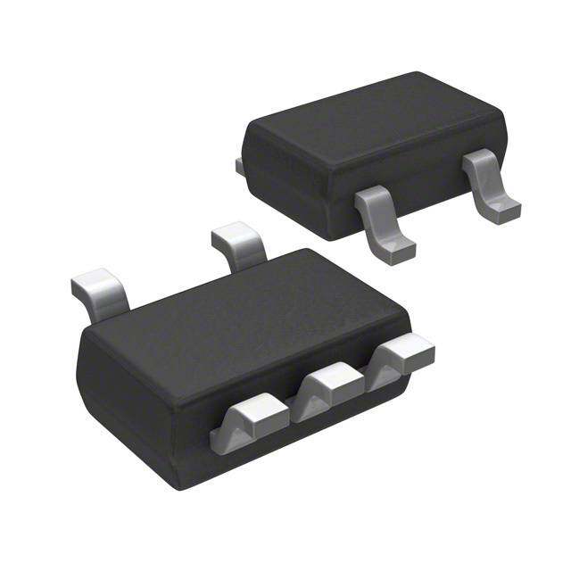
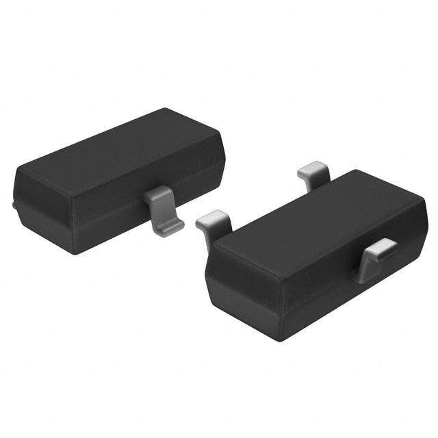
NCP431A, SC431A, NCP431B, SC431B, NCP432B, SC432B Series MARKING DIAGRAMS NCP43 8 1xxxx YWW(cid:2) N431xx xxx M(cid:2) ALYW (cid:2) (cid:2) (cid:2) 1 1 xx, xxx, xxx = Specific Device Code A = Assembly Location L = Wafer Lot Y = Year M = Date Code W, WW = Work Week (cid:2) = Pb−Free Package (Note: Microdot may be in either location) ORDERING INFORMATION Operating Device Marking Tolerance Temperature Range Package Shipping† NCP431ACDR2G AC 1% SOIC−8 2500 / Tape & Reel (Pb−Free) NCP431ACSNT1G VRF 1% SOT−23−3 3000 / Tape & Reel (Pb−Free) NCP431BCSNT1G VRJ 0.5% SOT−23−3 3000 / Tape & Reel 0°C to 70°C (Pb−Free) NCP432BCSNT1G VRM 0.5% SOT−23−3 3000 / Tape & Reel (Pb−Free) NCP431ACLPRAG ACLP 1% TO−92 (TO−226) 2000 / Tape & Reel (Pb−Free) NCP431AIDR2G AI 1% SOIC−8 2500 / Tape & Reel (Pb−Free) NCP431AISNT1G VRG 1% SOT−23−3 3000 / Tape & Reel (Pb−Free) NCP431BISNT1G VRK 0.5% SOT−23−3 3000 / Tape & Reel −40°C to 85°C (Pb−Free) NCP432BISNT1G VRN 0.5% SOT−23−3 3000 / Tape & Reel (Pb−Free) NCP431AILPRAG AILP 1% TO−92 (TO−226) 2000 / Tape & Reel (Pb−Free) NCP431AVDR2G AV 1% SOIC−8 2500 / Tape & Reel (Pb−Free) NCP431AVSNT1G / VRH 1% SOT−23−3 3000 / Tape & Reel SC431AVSNT1G* (Pb−Free) NCP431AVLPRAG AVLP 1% TO−92 (TO−226) 2000 / Tape & Reel (Pb−Free) −40°C to 125°C NCP431AVLPG AVLP 1% TO−92 (TO−226) 2000 Units / Bag (Pb−Free) NCP431BVSNT1G / VRL 0.5% SOT−23−3 3000 / Tape & Reel SC431BVSNT1G* (Pb−Free) NCP432BVSNT1G / VRP 0.5% SOT−23−3 3000 / Tape & Reel SC432BVSNT1G* (Pb−Free) †For information on tape and reel specifications, including part orientation and tape sizes, please refer to our Tape and Reel Packaging Specifications Brochure, BRD8011/D. *SC Prefix for Automotive and Other Applications Requiring Unique Site and Control Change Requirements; AEC−Q100 Qualified and PPAP Capable. www.onsemi.com 14
NCP431A, SC431A, NCP431B, SC431B, NCP432B, SC432B Series PACKAGE DIMENSIONS TO−92 (TO−226) CASE 29−11 ISSUE AN A NOTES: B STRAIGHT LEAD 1. DIMENSIONING AND TOLERANCING PER ANSI BULK PACK Y14.5M, 1982. 2. CONTROLLING DIMENSION: INCH. R 3. CONTOUR OF PACKAGE BEYOND DIMENSION R IS UNCONTROLLED. 4. LEAD DIMENSION IS UNCONTROLLED IN P AND P BEYOND DIMENSION K MINIMUM. L SEATING INCHES MILLIMETERS PLANE K DIM MIN MAX MIN MAX A 0.175 0.205 4.45 5.20 B 0.170 0.210 4.32 5.33 C 0.125 0.165 3.18 4.19 D 0.016 0.021 0.407 0.533 X X D G 0.045 0.055 1.15 1.39 G H 0.095 0.105 2.42 2.66 J 0.015 0.020 0.39 0.50 H J K 0.500 --- 12.70 --- L 0.250 --- 6.35 --- V C N 0.080 0.105 2.04 2.66 P --- 0.100 --- 2.54 SECTION X−X R 0.115 --- 2.93 --- 1 N V 0.135 --- 3.43 --- N R A B BENT LEAD N1O.TEDSIM:ENSIONING AND TOLERANCING PER TAPE & REEL ASME Y14.5M, 1994. 2. CONTROLLING DIMENSION: MILLIMETERS. AMMO PACK 3. CONTOUR OF PACKAGE BEYOND DIMENSION R IS UNCONTROLLED. 4. LEAD DIMENSION IS UNCONTROLLED IN P P AND BEYOND DIMENSION K MINIMUM. T MILLIMETERS SPELAATNIENG K DIM MIN MAX A 4.45 5.20 B 4.32 5.33 C 3.18 4.19 D 0.40 0.54 X X D G 2.40 2.80 G J 0.39 0.50 K 12.70 --- J N 2.04 2.66 V P 1.50 4.00 C R 2.93 --- V 3.43 --- SECTION X−X 1 N www.onsemi.com 15
NCP431A, SC431A, NCP431B, SC431B, NCP432B, SC432B Series PACKAGE DIMENSIONS SOIC−8 NB CASE 751−07 ISSUE AK NOTES: −X− 1. DIMENSIONING AND TOLERANCING PER ANSI Y14.5M, 1982. A 2. CONTROLLING DIMENSION: MILLIMETER. 3. DIMENSION A AND B DO NOT INCLUDE MOLD PROTRUSION. 4. MAXIMUM MOLD PROTRUSION 0.15 (0.006) 8 5 PER SIDE. 5. DIMENSION D DOES NOT INCLUDE DAMBAR B S 0.25 (0.010) M Y M PROTRUSION. ALLOWABLE DAMBAR PROTRUSION SHALL BE 0.127 (0.005) TOTAL 1 IN EXCESS OF THE D DIMENSION AT −Y− 4 K 6. 7M5A1X−I0M1U TMH RMUA T7E51R−IA0L6 CAROEN DOIBTSIOONL.ETE. NEW STANDARD IS 751−07. G MILLIMETERS INCHES DIM MIN MAX MIN MAX A 4.80 5.00 0.189 0.197 C NX 45(cid:3) B 3.80 4.00 0.150 0.157 SEATING C 1.35 1.75 0.053 0.069 PLANE D 0.33 0.51 0.013 0.020 −Z− G 1.27 BSC 0.050 BSC H 0.10 0.25 0.004 0.010 0.10 (0.004) J 0.19 0.25 0.007 0.010 H D M J K 0.40 1.27 0.016 0.050 M 0 (cid:3) 8 (cid:3) 0 (cid:3) 8 (cid:3) N 0.25 0.50 0.010 0.020 0.25 (0.010)M Z Y S X S S 5.80 6.20 0.228 0.244 SOLDERING FOOTPRINT* 1.52 0.060 7.0 4.0 0.275 0.155 0.6 1.270 0.024 0.050 (cid:5) (cid:6) mm SCALE 6:1 inches *For additional information on our Pb−Free strategy and soldering details, please download the ON Semiconductor Soldering and Mounting Techniques Reference Manual, SOLDERRM/D. www.onsemi.com 16
NCP431A, SC431A, NCP431B, SC431B, NCP432B, SC432B Series PACKAGE DIMENSIONS SOT−23 (TO−236) CASE 318−08 ISSUE AS D NOTES: 1. DIMENSIONING AND TOLERANCING PER ASME Y14.5M, 1994. 2. CONTROLLING DIMENSION: MILLIMETERS. 3. MAXIMUM LEAD THICKNESS INCLUDES LEAD FINISH. 0.25 MINIMUM LEAD THICKNESS IS THE MINIMUM THICKNESS OF 3 THE BASE MATERIAL. E HE T 4. DPRIMOETNRSUIOSINOSN DS, AONRD G EA DTEO BNUORTR INS.CLUDE MOLD FLASH, 1 2 MILLIMETERS INCHES DIM MIN NOM MAX MIN NOM MAX L A 0.89 1.00 1.11 0.035 0.039 0.044 3Xb L1 A1 0.01 0.06 0.10 0.000 0.002 0.004 b 0.37 0.44 0.50 0.015 0.017 0.020 e VIEW C c 0.08 0.14 0.20 0.003 0.006 0.008 TOP VIEW D 2.80 2.90 3.04 0.110 0.114 0.120 E 1.20 1.30 1.40 0.047 0.051 0.055 e 1.78 1.90 2.04 0.070 0.075 0.080 L 0.30 0.43 0.55 0.012 0.017 0.022 A L1 0.35 0.54 0.69 0.014 0.021 0.027 HE 2.10 2.40 2.64 0.083 0.094 0.104 T 0° −−− 10° 0° −−− 10° A1 c SIDE VIEW SEE VIEW C END VIEW RECOMMENDED SOLDERING FOOTPRINT* 3X 2.90 0.90 3X0.80 0.95 PITCH DIMENSIONS: MILLIMETERS *For additional information on our Pb−Free strategy and soldering details, please download the ON Semiconductor Soldering and Mounting Techniques Reference Manual, SOLDERRM/D. ON Semiconductor and are trademarks of Semiconductor Components Industries, LLC dba ON Semiconductor or its subsidiaries in the United States and/or other countries. ON Semiconductor owns the rights to a number of patents, trademarks, copyrights, trade secrets, and other intellectual property. A listing of ON Semiconductor’s product/patent coverage may be accessed at www.onsemi.com/site/pdf/Patent−Marking.pdf. ON Semiconductor reserves the right to make changes without further notice to any products herein. ON Semiconductor makes no warranty, representation or guarantee regarding the suitability of its products for any particular purpose, nor does ON Semiconductor assume any liability arising out of the application or use of any product or circuit, and specifically disclaims any and all liability, including without limitation special, consequential or incidental damages. Buyer is responsible for its products and applications using ON Semiconductor products, including compliance with all laws, regulations and safety requirements or standards, regardless of any support or applications information provided by ON Semiconductor. “Typical” parameters which may be provided in ON Semiconductor data sheets and/or specifications can and do vary in different applications and actual performance may vary over time. All operating parameters, including “Typicals” must be validated for each customer application by customer’s technical experts. ON Semiconductor does not convey any license under its patent rights nor the rights of others. ON Semiconductor products are not designed, intended, or authorized for use as a critical component in life support systems or any FDA Class 3 medical devices or medical devices with a same or similar classification in a foreign jurisdiction or any devices intended for implantation in the human body. Should Buyer purchase or use ON Semiconductor products for any such unintended or unauthorized application, Buyer shall indemnify and hold ON Semiconductor and its officers, employees, subsidiaries, affiliates, and distributors harmless against all claims, costs, damages, and expenses, and reasonable attorney fees arising out of, directly or indirectly, any claim of personal injury or death associated with such unintended or unauthorized use, even if such claim alleges that ON Semiconductor was negligent regarding the design or manufacture of the part. ON Semiconductor is an Equal Opportunity/Affirmative Action Employer. This literature is subject to all applicable copyright laws and is not for resale in any manner. PUBLICATION ORDERING INFORMATION LITERATURE FULFILLMENT: N. American Technical Support: 800−282−9855 Toll Free ON Semiconductor Website: www.onsemi.com Literature Distribution Center for ON Semiconductor USA/Canada 19521 E. 32nd Pkwy, Aurora, Colorado 80011 USA Europe, Middle East and Africa Technical Support: Order Literature: http://www.onsemi.com/orderlit Phone: 303−675−2175 or 800−344−3860 Toll Free USA/Canada Phone: 421 33 790 2910 Fax: 303−675−2176 or 800−344−3867 Toll Free USA/Canada For additional information, please contact your local Email: orderlit@onsemi.com Sales Representative ◊ www.onsemi.com NCP431/D 17