ICGOO在线商城 > 集成电路(IC) > 数据采集 - 模数转换器 > AD574AJDZ
 Datasheet下载
- 型号: AD574AJDZ
- 制造商: Analog
- 库位|库存: xxxx|xxxx
- 要求:
| 数量阶梯 | 香港交货 | 国内含税 |
| +xxxx | $xxxx | ¥xxxx |
查看当月历史价格
查看今年历史价格
AD574AJDZ产品简介:
ICGOO电子元器件商城为您提供AD574AJDZ由Analog设计生产,在icgoo商城现货销售,并且可以通过原厂、代理商等渠道进行代购。 AD574AJDZ价格参考¥509.33-¥509.33。AnalogAD574AJDZ封装/规格:数据采集 - 模数转换器, 12 Bit Analog to Digital Converter 1 Input 1 SAR 28-CDIP。您可以下载AD574AJDZ参考资料、Datasheet数据手册功能说明书,资料中有AD574AJDZ 详细功能的应用电路图电压和使用方法及教程。
AD574AJDZ是由Analog Devices Inc.(模拟器件公司)生产的一款12位模数转换器(ADC),属于数据采集系统中的关键组件。它广泛应用于需要高精度、高速度和可靠性的数据采集场景中,特别是在工业控制、医疗设备、通信系统等领域。

 应用场景:

1. 工业自动化与控制:
   AD574AJDZ在工业自动化领域中用于将传感器采集到的模拟信号(如温度、压力、位移等)转换为数字信号,以便微处理器或计算机进行处理和分析。它能够实时监测生产线上的各种参数,确保系统的稳定性和安全性。例如,在温度控制系统中,AD574AJDZ可以精确地将热电偶输出的电压信号转换为对应的温度值,从而实现精准的温度控制。

2. 医疗设备:
   在医疗设备中,AD574AJDZ可用于心电图(ECG)、脑电图(EEG)等生理信号的采集。这些设备需要高精度的ADC来确保信号的准确性和可靠性,以帮助医生做出正确的诊断。此外,AD574AJDZ还可以用于超声波成像设备中,将探头接收到的模拟信号转换为数字信号,以便后续处理和图像生成。

3. 通信系统:
   在通信系统中,AD574AJDZ可以用于信号调制解调器(Modem)中,将接收到的模拟信号转换为数字信号,以便进一步处理和传输。它还适用于无线电接收机、卫星通信等场景,确保信号的高质量传输和接收。

4. 测试与测量仪器:
   AD574AJDZ广泛应用于各种测试与测量仪器中,如示波器、频谱分析仪等。这些仪器需要高精度的ADC来捕捉和分析复杂的电信号。AD574AJDZ的高分辨率和快速转换速度使其成为理想的选择,能够提供准确的测量结果。

5. 汽车电子:
   在汽车电子系统中,AD574AJDZ可用于车载传感器的数据采集,如发动机温度、油压、车速等。通过将这些模拟信号转换为数字信号,车辆的电子控制单元(ECU)可以实时监控并调整车辆的运行状态,提高驾驶的安全性和舒适性。

总之,AD574AJDZ凭借其高精度、高速度和可靠性,适用于多种对数据采集要求较高的应用场景,能够为各类系统提供稳定可靠的模数转换功能。
| 参数 | 数值 |
| 产品目录 | 集成电路 (IC)半导体 |
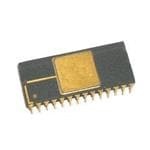
| 描述 | IC ADC 12BIT W/REF 28-CDIP模数转换器 - ADC IC MONO 12-BIT |
| 产品分类 | |
| 品牌 | Analog Devices |
| 产品手册 | |
| 产品图片 |
|
| rohs | 符合RoHS无铅 / 符合限制有害物质指令(RoHS)规范要求 |
| 产品系列 | 数据转换器IC,模数转换器 - ADC,Analog Devices AD574AJDZ- |
| 数据手册 | |
| 产品型号 | AD574AJDZ |
| 产品种类 | 模数转换器 - ADC |
| 位数 | 12 |
| 供应商器件封装 | 28-CDIP |
| 分辨率 | 12 bit |
| 包装 | 管件 |
| 商标 | Analog Devices |
| 安装类型 | 通孔 |
| 安装风格 | Through Hole |
| 封装 | Tube |
| 封装/外壳 | 28-CDIP(0.605",15.37mm) |
| 封装/箱体 | CDIP-28 SB |
| 工作温度 | 0°C ~ 70°C |
| 工作电源电压 | 5 V, 15 V |
| 工厂包装数量 | 13 |
| 接口类型 | Parallel |
| 数据接口 | 并联 |
| 最大功率耗散 | 725 mW |
| 最大工作温度 | + 125 C |
| 最小工作温度 | - 55 C |
| 标准包装 | 13 |
| 电压参考 | Internal, External |
| 电压源 | 模拟和数字,双 ± |
| 系列 | AD574A |
| 结构 | SAR |
| 转换器数 | 1 |
| 转换器数量 | 1 |
| 输入数和类型 | 2 个单端,单极2 个单端,双极 |
| 输入类型 | Single-Ended |
| 通道数量 | 1 Channel |
| 采样率(每秒) | - |


- 商务部:美国ITC正式对集成电路等产品启动337调查
- 曝三星4nm工艺存在良率问题 高通将骁龙8 Gen1或转产台积电
- 太阳诱电将投资9.5亿元在常州建新厂生产MLCC 预计2023年完工
- 英特尔发布欧洲新工厂建设计划 深化IDM 2.0 战略
- 台积电先进制程称霸业界 有大客户加持明年业绩稳了
- 达到5530亿美元!SIA预计今年全球半导体销售额将创下新高
- 英特尔拟将自动驾驶子公司Mobileye上市 估值或超500亿美元
- 三星加码芯片和SET,合并消费电子和移动部门,撤换高东真等 CEO
- 三星电子宣布重大人事变动 还合并消费电子和移动部门
- 海关总署:前11个月进口集成电路产品价值2.52万亿元 增长14.8%


PDF Datasheet 数据手册内容提取
None
AD574A–SPECIFICATIONS (@ +25(cid:56)C with V = +15 V or +12 V, V = +5 V, V = –15 V or –12 V CC LOGIC EE unless otherwise noted) AD574AJ AD574AK AD574AL Model Min Typ Max Min Typ Max Min Typ Max Units RESOLUTION 12 12 12 Bits LINEARITY ERROR @ +25(cid:176)C – 1 – 1/2 – 1/2 LSB T to T – 1 – 1/2 – 1/2 LSB MIN MAX DIFFERENTIAL LINEARITY ERROR (Minimum Resolution for Which No Missing Codes are Guaranteed) T to T 11 12 12 Bits MIN MAX UNIPOLAR OFFSET (Adjustable to Zero) – 2 – 1 – 1 LSB BIPOLAR OFFSET (Adjustable to Zero) – 4 – 4 – 2 LSB FULL-SCALE CALIBRATION ERROR (With Fixed 50 W Resistor from REF OUT to REF IN) (Adjustable to Zero) 0.25 0.25 0.125 % of FS TEMPERATURE RANGE 0 +70 0 +70 0 +70 (cid:176)C TEMPERATURE COEFFICIENTS (Using Internal Reference) T to T MIN MAX Unipolar Offset – 2 (10) – 1 (5) – 1 (5) LSB (ppm/(cid:176)C) Bipolar Offset – 2 (10) – 1 (5) – 1 (5) LSB (ppm/(cid:176)C) Full-Scale Calibration – 9 (50) – 5 (27) – 2 (10) LSB (ppm/(cid:176)C) POWER SUPPLY REJECTION Max Change in Full-Scale Calibration V = 15 V – 1.5 V or 12 V – 0.6 V – 2 – 1 – 1 LSB CC V = 5 V – 0.5 V – 1/2 – 1/2 – 1/2 LSB LOGIC V = –15 V – 1.5 V or –12 V – 0.6 V – 2 – 1 – 1 LSB EE ANALOG INPUT Input Ranges Bipolar –5 +5 –5 +5 –5 +5 Volts –10 +10 –10 +10 –10 +10 Volts Unipolar 0 +10 0 +10 0 +10 Volts 0 +20 0 +20 0 +20 Volts Input Impedance 10 Volt Span 3 5 7 3 5 7 3 5 7 kW 20 Volt Span 6 10 14 6 10 14 6 10 14 kW DIGITAL CHARACTERISTICS1 (T –T ) MIN MAX Inputs2 (CE, CS, R/C, A) 0 Logic “1” Voltage +2.0 +5.5 +2.0 +5.5 +2.0 +5.5 Volts Logic “0” Voltage –0.5 +0.8 –0.5 +0.8 –0.5 +0.8 Volts Current –20 +20 –20 +20 –20 +20 m A Capacitance 5 5 5 pF Output (DB11–DB0, STS) Logic “1” Voltage (I £ 500 m A) +2.4 +2.4 +2.4 Volts SOURCE Logic “0” Voltage (I £ 1.6 mA) +0.4 +0.4 +0.4 Volts SINK Leakage (DB11–DB0, High-Z State) –20 +20 –20 +20 –20 +20 m A Capacitance 5 5 5 pF POWER SUPPLIES Operating Range V +4.5 +5.5 +4.5 +5.5 +4.5 +5.5 Volts LOGIC V +11.4 +16.5 +11.4 +16.5 +11.4 +16.5 Volts CC V –11.4 –16.5 –11.4 –16.5 –11.4 –16.5 Volts EE Operating Current I 30 40 30 40 30 40 mA LOGIC I 2 5 2 5 2 5 mA CC I 18 30 18 30 18 30 mA EE POWER DISSIPATION 390 725 390 725 390 725 mW INTERNAL REFERENCE VOLTAGE 9.98 10.0 10.02 9.98 10.0 10.02 9.99 10.0 10.01 Volts Output Current (Available for External Loads)3 1.5 1.5 1.5 mA (External Load Should not Change During Conversion) PACKAGE OPTIONS4 Ceramic (D-28) AD574ASD AD574AKD AD574ALD Plastic (N-28) AD574AJN AD574AKN AD574ALN PLCC (P-28A) AD574AJP AD574AKP LCC (E-28A) AD574AJE AD574AKE NOTES 1Detailed Timing Specifications appear in the Timing Section. 212/8 Input is not TTL-compatible and must be hard wired to V or Digital Common. LOGIC 3The reference should be buffered for operation on – 12 V supplies. 4D = Ceramic DIP; N = Plastic DIP; P = Plastic Leaded Chip Carrier. Specifications subject to change without notice. –2– REV. B
AD574A AD574AS AD574AT AD574AU Model Min Typ Max Min Typ Max Min Typ Max Units RESOLUTION 12 12 12 Bits LINEARITY ERROR @ +25(cid:176)C – 1 – 1/2 – 1/2 LSB T to T – 1 – 1 – 1 LSB MIN MAX DIFFERENTIAL LINEARITY ERROR (Minimum Resolution for Which No Missing Codes are Guaranteed) T to T 11 12 12 Bits MIN MAX UNIPOLAR OFFSET (Adjustable to Zero) – 2 – 1 – 1 LSB BIPOLAR OFFSET (Adjustable to Zero) – 4 – 4 – 2 LSB FULL-SCALE CALIBRATION ERROR (With Fixed 50 W Resistor from REF OUT to REF IN) (Adjustable to Zero) 0.25 0.25 0.125 % of FS TEMPERATURE RANGE –55 +125 –55 +125 –55 +125 (cid:176)C TEMPERATURE COEFFICIENTS (Using Internal Reference) (T to T ) MIN MAX Unipolar Offset – 2 (5) – 1 (2.5) – 1 (2.5) LSB (ppm/(cid:176)C) Bipolar Offset – 4 (10) – 2 (5) – 1 (2.5) LSB (ppm/(cid:176)C) Full-Scale Calibration – 20 (50) – 10 (25) – 5 (12.5) LSB (ppm/(cid:176)C) POWER SUPPLY REJECTION Max Change in Full-Scale Calibration V = 15 V – 1.5 V or 12 V – 0.6 V – 2 – 1 – 1 LSB CC V = 5 V – 0.5 V – 1/2 – 1/2 – 1/2 LSB LOGIC V = –15 V – 1.5 V or –12 V – 0.6 V – 2 – 1 – 1 LSB EE ANALOG INPUT Input Ranges Bipolar –5 +5 –5 +5 –5 +5 Volts –10 +10 –10 +10 –10 +10 Volts Unipolar 0 +10 0 +10 0 +10 Volts 0 +20 0 +20 0 +20 Volts Input Impedance 10 Volt Span 3 5 7 3 5 7 3 5 7 kW 20 Volt Span 6 10 14 6 10 14 6 10 14 kW DIGITAL CHARACTERISTICS1 (T –T ) MIN MAX Inputs2 (CE, CS, R/C, A) 0 Logic “1” Voltage +2.0 +5.5 +2.0 +5.5 +2.0 +5.5 Volts Logic “0” Voltage –0.5 +0.8 –0.5 +0.8 –0.5 +0.8 Volts Current –20 +20 –20 +20 –20 +20 m A Capacitance 5 5 5 pF Output (DB11–DB0, STS) Logic “1” Voltage (I £ 500 m A) +2.4 +2.4 +2.4 Volts SOURCE Logic “0” Voltage (I £ 1.6 mA) +0.4 +0.4 +0.4 Volts SINK Leakage (DB11–DB0, High-Z State) –20 +20 –20 +20 –20 +20 m A Capacitance 5 5 5 pF POWER SUPPLIES Operating Range V +4.5 +5.5 +4.5 +5.5 +4.5 +5.5 Volts LOGIC V +11.4 +16.5 +11.4 +16.5 +11.4 +16.5 Volts CC V –11.4 –16.5 –11.4 –16.5 –11.4 –16.5 Volts EE Operating Current I 30 40 30 40 30 40 mA LOGIC I 2 5 2 5 2 5 mA CC I 18 30 18 30 18 30 mA EE POWER DISSIPATION 390 725 390 725 390 725 mW INTERNAL REFERENCE VOLTAGE 9.98 10.0 10.02 9.98 10.0 10.02 9.99 10.0 10.01 Volts Output Current (Available for External Loads)3 1.5 1.5 1.5 mA (External Load Should not Change During Conversion) PACKAGE OPTION4 Ceramic (D-28) AD574ASD AD574ATD AD574AUD NOTES 1Detailed Timing Specifications appear in the Timing Section. 212/8 Input is not TTL-compatible and must be hard wired to V or Digital Common. LOGIC 3The reference should be buffered for operation on – 12 V supplies. 4D = Ceramic DIP. Specifications subject to change without notice. REV. B –3–
AD574A +5V SUVPLPOLGYIC 1 28 SSTTASTUS DATA MODE SELECT 2 MSB 27 DB11 12/8 N MSB BYTCEH IAPD SDERLEESCCSST/ 3 CONTROL 3 BBI 26 DB10 SHORT CYCLAEO 4 ST EL 25 DB9 READ/CONVERT 5 CLOCK SAR 12 A A 24 DB8 R/C T CHIP ENABCLEE 6 3k OE NI 23 DB7 +12/+15V SUPPLY 7 U B 22 DB6 DIGITAL A+N1A0VLO RGE FCREOERMFE MONVOCUCNETC 89 1R0EVF IDCIADCOA C=MP 12 PUTT BBEL 2210 DDBB54 DOAUTTAPUTS AC 4 x N x IREF B RBE-FI1PE2OR/-LE1A5NRVC SOEU RFINPFEPSPFVUE LIENYTTE 111012 199..9955kk IREF 8k UERSFF NBBELI 111987 DDDBBB321 BIP OFF 10V SPAN IN1P0VUITN 13 5k DAC N VEE LCSB 16 DLSBB0 5k 20V SPAN IN2P0VUITN 14 AD574A 12 15 DDICGITAL COMMON AD574A Block Diagram and Pin Configuration ABSOLUTE MAXIMUM RATINGS* (Specifications apply to all grades, except where noted) V to Digital Common . . . . . . . . . . . . . . . . . .0 V to +16.5 V Chip Temperature . . . . . . . . . . . . . . . . . . . . . . . . . . . . . 175(cid:176) C CC V to Digital Common . . . . . . . . . . . . . . . . . . .0 V to –16.5 V Power Dissipation . . . . . . . . . . . . . . . . . . . . . . . . . . . .825 mW EE V to Digital Common . . . . . . . . . . . . . . . . . . 0 V to +7 V Lead Temperature (Soldering, 10 sec). . . . . . . . . . . . . +300(cid:176) C LOGIC Analog Common to Digital Common . . . . . . . . . . . . . . . – 1 V Storage Temperature (Ceramic) . . . . . . . . . .–65(cid:176) C to +150(cid:176) C Control Inputs (CE, CS, A 12/8, R/C) to (Plastic) . . . . . . . . . . . . . . . . . . . . . . . . . . .–25(cid:176) C to +100(cid:176) C O Digital Common . . . . . . . . . . . . . .–0.5 V to V + 0.5 V *Stresses above those listed under “Absolute Maximum Ratings” may cause LOGIC Analog Inputs (REF IN, BIP OFF, 10 V ) to permanent damage to the device. This is a stress rating only and functional IN operation of the device at these or any other conditions above those indicated in the Analog Common . . . . . . . . . . . . . . . . . . . . . . . . .V to V EE CC operational sections of this specification is not implied. Exposure to absolute 20 V to Analog Common . . . . . . . . . . . . . . . . . . . . . . – 24 V IN maximum rating conditions for extended periods may affect device reliability. REF OUT . . . . . . . . . . . . . . . . . .Indefinite Short to Common Momentary Short to V CC ORDERING GUIDE Resolution Max Temperature Linearity Error No Missing Codes Full Scale Model1 Range Max (T to T ) (T to T ) T.C. (ppm/(cid:176) C) MIN MAX MIN MAX AD574AJ(X) 0(cid:176) C to +70(cid:176) C – 1 LSB 11 Bits 50.0 AD574AK(X) 0(cid:176) C to +70(cid:176) C – 1/2 LSB 12 Bits 27.0 AD574AL(X) 0(cid:176) C to +70(cid:176) C – 1/2 LSB 12 Bits 10.0 AD574AS(X)2 –55(cid:176) C to +125(cid:176) C – 1 LSB 11 Bits 50.0 AD574AT(X)2 –55(cid:176) C to +125(cid:176) C – 1 LSB 12 Bits 25.0 AD574AU(X)2 –55(cid:176) C to +125(cid:176) C – 1 LSB 12 Bits 12.5 NOTES 1X = Package designator. Available packages are: D (D-28) for all grades. E (E-28A) for J and K grades and /883B processed S, T and U grades. N (N-28) for J, K, and L grades. P (P-28A) for PLCC in J, K grades. Example: AD574AKN is K grade in plastic DIP. 2For details on grade and package offerings screened in accordance with MIL-STD-883, refer to Analog Devices Military Products Databook. –4– REV. B
AD574A THE AD574A OFFERS GUARANTEED MAXIMUM LINEARITY ERROR OVER THE FULL OPERATING TEMPERATURE RANGE DEFINITIONS OF SPECIFICATIONS QUANTIZATION UNCERTAINTY Analog-to-digital converters exhibit an inherent quantization LINEARITY ERROR uncertainty of – 1/2 LSB. This uncertainty is a fundamental Linearity error refers to the deviation of each individual code characteristic of the quantization process and cannot be reduced from a line drawn from “zero” through “full scale”. The point for a converter of given resolution. used as “zero” occurs 1/2 LSB (1.22 mV for 10 volt span) be- fore the first code transition (all zeros to only the LSB “on”). LEFT-JUSTIFIED DATA “Full scale” is defined as a level 1 1/2 LSB beyond the last code The data format used in the AD574A is left-justified. This transition (to all ones). The deviation of a code from the true means that the data represents the analog input as a fraction of straight line is measured from the middle of each particular code. (cid:52)(cid:48)(cid:57)(cid:53) full-scale, ranging from 0 to . This implies a binary point (cid:52)(cid:48)(cid:57)(cid:54) The AD574AK, L, T, and U grades are guaranteed for maxi- to the left of the MSB. mum nonlinearity of – 1/2 LSB. For these grades, this means that an analog value which falls exactly in the center of a given FULL-SCALE CALIBRATION ERROR code width will result in the correct digital output code. Values The last transition (from 1111 1111 1110 to 1111 1111 1111) nearer the upper or lower transition of the code width may pro- should occur for an analog value 1 1/2 LSB below the nominal duce the next upper or lower digital output code. The AD574AJ and S grades are guaranteed to – 1 LSB max error. For these full scale (9.9963 volts for 10.000 volts full scale). The full-scale calibration error is the deviation of the actual level at the last grades, an analog value which falls within a given code width transition from the ideal level. This error, which is typically will result in either the correct code for that region or either 0.05% to 0.1% of full scale, can be trimmed out as shown in adjacent one. Figures 3 and 4. Note that the linearity error is not user-adjustable. TEMPERATURE COEFFICIENTS DIFFERENTIAL LINEARITY ERROR (NO MISSING The temperature coefficients for full-scale calibration, unipolar CODES) offset, and bipolar offset specify the maximum change from the A specification which guarantees no missing codes requires that initial (25(cid:176) C) value to the value at T or T . MIN MAX every code combination appear in a monotonic increasing se- quence as the analog input level is increased. Thus every code POWER SUPPLY REJECTION must have a finite width. For the AD574AK, L, T, and U The standard specifications for the AD574A assume use of grades, which guarantee no missing codes to 12-bit resolution, +5.00 V and – 15.00 V or – 12.00 V supplies. The only effect of all 4096 codes must be present over the entire operating tem- power supply error on the performance of the device will be a perature ranges. The AD574AJ and S grades guarantee no miss- small change in the full-scale calibration. This will result in a ing codes to 11-bit resolution over temperature; this means that linear change in all lower order codes. The specifications show all code combinations of the upper 11 bits must be present; in the maximum full-scale change from the initial value with the practice very few of the 12-bit codes are missing. supplies at the various limits. UNIPOLAR OFFSET CODE WIDTH The first transition should occur at a level 1/2 LSB above analog A fundamental quantity for A/D converter specifications is the common. Unipolar offset is defined as the deviation of the actual code width. This is defined as the range of analog input values transition from that point. This offset can be adjusted as discussed for which a given digital output code will occur. The nominal on the following two pages. The unipolar offset temperature value of a code width is equivalent to 1 least significant bit coefficient specifies the maximum change of the transition point (LSB) of the full-scale range or 2.44 mV out of 10 volts for a over temperature, with or without external adjustment. 12-bit ADC. BIPOLAR OFFSET In the bipolar mode the major carry transition (0111 1111 1111 to 1000 0000 0000) should occur for an analog value 1/2 LSB below analog common. The bipolar offset error and temperature coefficient specify the initial deviation and maximum change in the error over temperature. REV. B –5–
AD574A CIRCUIT OPERATION DRIVING THE AD574 ANALOG INPUT The AD574A is a complete 12-bit A/D converter which requires The internal circuitry of the AD574 dictates that its analog no external components to provide the complete successive- input be driven by a low source impedance. Voltage changes at approximation analog-to-digital conversion function. A block the current summing node of the internal comparator result in diagram of the AD574A is shown in Figure 1. abrupt modulations of the current at the analog input. For accu- rate 12-bit conversions the driving source must be capable of holding a constant output voltage under these dynamically +5V SUVPLPOLGYIC 1 28 SSTTASTUS changing load conditions. DATA MODE SELE12C/T8 2 MNSB 27 DMBS1B1 BYTCEH IAPD SDERLEESCCSST/ 3 CONTROL 3 BBI 26 DB10 FEEDBACK TO AMPLIFIER SHORT CYCLAEO 4 ST EL 25 DB9 V+ READ/CONVERT 5 CLOCK SAR 12 A A 24 DB8 R/C T A++N11A02VL/C+O RH1G5EIP VFCR EESOERNUMFEAP MONBPVOCCULLCNEEEYTC 6789 1R0EVF 3k IDCIADCOA C=MP 12 OEUPUTT BNBBELI 22223210 DDDDBBBB7654 DDOIAUGTTIATPAULTS RCLEUISMRISIRTTIENONGRTS RIN IIAND574ACOUURTRPEUNTT RBE12-FI1P00E2OVVR/- LE1SSA5NPPRVAAC NNSOEBU R IFIIIPNNNPFE12 POPPSPF00VAUVVUUE LFIECNYIITTFTTNNE 1111140123 199..995555kkkk AD57IRD4EA4AF Cx N1N x2 IRE8FkVEE BUERSFF LCNBBESLIB 1111159876 DDDDLDDSICBBBBGB3021ITAL COMMON ANALOFGi gCOuVM–rMeON 2ICAROINHMEP. ISAESPPN NLMOOI GFLONEIOEDSSpORUE IP LN P L AO UIATMTULEEISTSTDmEPET UB DLCTY OUBp IARYMDR PE–END TAA.NCDE.5i7DIF4FA IniTCtESeOTMrPfAaRcAeTDOSAARCR The output impedance of an op amp has an open-loop value Figure 1.Block Diagram of AD574A 12-Bit A-to-D Converter which, in a closed loop, is divided by the loop gain available at When the control section is commanded to initiate a conversion the frequency of interest. The amplifier should have acceptable (as described later), it enables the clock and resets the successive- loop gain at 500 kHz for use with the AD574A. To check approximation register (SAR) to all zeros. Once a conversion whether the output properties of a signal source are suitable, cycle has begun, it cannot be stopped or restarted and data is monitor the AD574’s input with an oscilloscope while a conver- not available from the output buffers. The SAR, timed by the sion is in progress. Each of the 12 disturbances should subside clock, will sequence through the conversion cycle and return an in 1 m s or less. end-of-convert flag to the control section. The control section For applications involving the use of a sample-and-hold ampli- will then disable the clock, bring the output status flag low, and fier, the AD585 is recommended. The AD711 or AD544 op enable control functions to allow data read functions by external amps are recommended for dc applications. command. SAMPLE-AND-HOLD AMPLIFIERS During the conversion cycle, the internal 12-bit current output Although the conversion time of the AD574A is a maximum of DAC is sequenced by the SAR from the most significant bit 35 m s, to achieve accurate 12-bit conversions of frequencies (MSB) to least significant bit (LSB) to provide an output cur- greater than a few Hz requires the use of a sample-and-hold rent which accurately balances the input signal current through the 5 kW (or 10 kW ) input resistor. The comparator determines amplifier (SHA). If the voltage of the analog input signal driving the AD574A changes by more than 1/2 LSB over the time whether the addition of each successively-weighted bit current interval needed to make a conversion, then the input requires a causes the DAC current sum to be greater or less than the input SHA. current; if the sum is less, the bit is left on; if more, the bit is turned off. After testing all the bits, the SAR contains a 12-bit The AD585 is a high linearity SHA capable of directly driving binary code which accurately represents the input signal to the analog input of the AD574A. The AD585’s fast acquisition within – 1/2 LSB. time, low aperture and low aperture jitter are ideally suited for high-speed data acquisition systems. Consider the AD574A The temperature-compensated buried Zener reference provides converter with a 35 m s conversion time and an input signal of the primary voltage reference to the DAC and guarantees excel- 10 V p-p: the maximum frequency which may be applied to lent stability with both time and temperature. The reference is trimmed to 10.00 volts – 0.2%; it can supply up to 1.5 mA to an achieve rated accuracy is 1.5 Hz. However, with the addition of an AD585, as shown in Figure 3, the maximum frequency external load in addition to the requirements of the reference in- increases to 26 kHz. put resistor (0.5 mA) and bipolar offset resistor (1 mA) when the AD574A is powered from – 15 V supplies. If the AD574A is The AD585’s low output impedance, fast-loop response, and used with – 12 V supplies, or if external current must be sup- low droop maintain 12-bits of accuracy under the changing load plied over the full temperature range, an external buffer ampli- conditions that occur during a conversion, making it suitable for fier is recommended. Any external load on the AD574A use in high accuracy conversion systems. Many other SHAs reference must remain constant during conversion. The cannot achieve 12-bits of accuracy and can thus compromise a thin-film application resistors are trimmed to match the system. The AD585 is recommended for AD574A applications full-scale output current of the DAC. There are two 5 kW input requiring a sample and hold. scaling resistors to allow either a 10 volt or 20 volt span. The An alternate approach is to use the AD1674, which combines 10 kW bipolar offset resistor is grounded for unipolar operation the ADC and SHA on one chip, with a total throughput time of and connected to the 10 volt reference for bipolar operation. 10 m s. –6– REV. B
AD574A +VS +15V page. Analog input connections and calibration are easily ac- TO A1 C1 + + +5V complished; the unipolar operating mode is shown in Figure 4. + C3 VREF –VS A C2 –15V AGND TO A1 2 12/8 STS 28 11 1 2 6 7 +VS R2 8 OFRFS1ET 3 CS HIGH 27 14 13 12 11 10 9 8 100W 12-BIT 100k 4 AO BIT 24 10k10k GAIN 10 3-DSATTAATE –12V/–15V +12V/+15V 5 R/C MIDDLE 23 13 A2 27 6 CE BITS 20 100ApDAF5185 OFF1S0+RE01Tk15V 1RR0043k 192AD574A 16 100k GRA2IN 10 REF IAND574A LBOITWS 1196 –15V100W 3 100W 8 REF OUT 1 2 3 4 5 6 7 4 100W 12 BIP OFF 15 AINNPAULTOG –VS A 28 5 0V TO +10V 0 TO +10V +5V 1 STATUS 13 10VIN CONVERT 7404 OR EQ. ANALOG +15V 7 N1.O CT1E, C2, C3 ARE 47(cid:109)m F TANTALUM, BYPASSED BY INPUT0S TO +20V 14 20VIN –15V 11 0.1(cid:109)m F CERAMIC. LOCATE AT ASSOCIATED A2 PINS. 9 ANA COM DIG COM 15 Figure 3.AD574A with AD585 Sample and Hold SUPPLY DECOUPLING AND LAYOUT CONSIDERATIONS Figure 4.Unipolar Input Connections It is critically important that the AD574A power supplies be fil- All of the thin-film application resistors of the AD574A are tered, well regulated, and free from high frequency noise. Use of trimmed for absolute calibration. Therefore, in many applica- noisy supplies will cause unstable output codes. Switching tions, no calibration trimming will be required. The absolute power supplies are not recommended for circuits attempting to accuracy for each grade is given in the specification tables. achieve 12-bit accuracy unless great care is used in filtering any For example, if no trims are used, the AD574AK guarantees switching spikes present in the output. Remember that a few – 1 LSB max zero offset error and – 0.25% (10 LSB) max millivolts of noise represents several counts of error in a 12-bit full-scale error. (Typical full-scale error is – 2 LSB.) If the offset ADC. trim is not required, Pin 12 can be connected directly to Pin 9; Decoupling capacitors should be used on all power supply pins; the two resistors and trimmer for Pin 12 are then not needed. If the +5 V supply decoupling capacitor should be connected the full-scale trim is not needed, a 50 W – 1% metal film resistor directly from Pin 1 to Pin 15 (digital common) and the +V should be connected between Pin 8 and Pin 10. CC and –V pins should be decoupled directly to analog common EE The analog input is connected between Pin 13 and Pin 9 for a (Pin 9). A suitable decoupling capacitor is a 4.7 m F tantalum 0 V to +10 V input range, between 14 and Pin 9 for a 0 V to type in parallel with a 0.1 m F disc ceramic type. +20 V input range. The AD574A easily accommodates an input Circuit layout should attempt to locate the AD574A, associated signal beyond the supplies. For the 10 volt span input, the LSB analog input circuitry, and interconnections as far as possible has a nominal value of 2.44 mV; for the 20 volt span, 4.88 mV. from logic circuitry. For this reason, the use of wire-wrap circuit If a 10.24 V range is desired (nominal 2.5 mV/bit), the gain construction is not recommended. Careful printed circuit con- trimmer (R2) should be replaced by a 50 W resistor, and a struction is preferred. 200 W trimmer inserted in series with the analog input to Pin 13 for a full-scale range of 20.48 V (5 mV/bit), use a 500 W trim- GROUNDING CONSIDERATIONS mer into Pin 14. The gain trim described below is now done The analog common at Pin 9 is the ground reference point for with these trimmers. The nominal input impedance into Pin 13 the internal reference and is thus the “high quality” ground for is 5 kW , and 10 kW into Pin 14. the AD574A; it should be connected directly to the analog refer- ence point of the system. In order to achieve all of the high UNIPOLAR CALIBRATION accuracy performance available from the AD574A in an envi- The AD574A is intended to have a nominal 1/2 LSB offset so ronment of high digital noise content, the analog and digital that the exact analog input for a given code will be in the middle commons should be connected together at the package. In some of that code (halfway between the transitions to the codes above situations, the digital common at Pin 15 can be connected to and below it). Thus, the first transition (from 0000 0000 0000 the most convenient ground reference point; analog power to 0000 0000 0001) will occur for an input level of +1/2 LSB return is preferred. (1.22 mV for 10 V range). If Pin 12 is connected to Pin 9, the unit will behave in this man- UNIPOLAR RANGE CONNECTIONS FOR THE AD574A ner, within specifications. If the offset trim (R1) is used, it The AD574A contains all the active components required to should be trimmed as above, although a different offset can be perform a complete 12-bit A/D conversion. Thus, for most situ- set for a particular system requirement. This circuit will give ap- ations, all that is necessary is connection of the power supplies proximately – 15 mV of offset trim range. (+5 V, +12 V/+15 V and –12 V/–15 V), the analog input, and the conversion initiation command, as discussed on the next REV. B –7–
AD574A The full-scale trim is done by applying a signal 1 1/2 LSB below the nominal full scale (9.9963 for a 10 V range). Trim R2 to START CONVERT give the last transition (1111 1111 1110 to 1111 1111 1111). BIPOLAR OPERATION STATUS LOW IF CONVERSION The connections for bipolar ranges are shown in Figure 5. IN PROGRESS R/C CONVERT Again, as for the unipolar ranges, if the offset and gain specifica- CE CS tions are sufficient, one or both of the trimmers shown can be VALUE OF A0 replaced by a 50 W – 1% fixed resistor. Bipolar calibration is A0 ACTO MLAMSATN CDONVERT similar to unipolar calibration. First, a signal 1/2 LSB above negative full scale (–4.9988 V for the – 5 V range) is applied and READ EEOOCC812 NFORTOEM 1 R1 is trimmed to give the first transition (0000 0000 0000 to 0000 0000 0001). Then a signal 1 1/2 LSB below positive full NIBBLE A, B, 12/8 ENABLE scale (+4.9963 V the – 5 V range) is applied and R2 trimmed to (NOTE 2) NIBBLE C TO OUTPUT give the last transition (1111 11111110 to 1111 1111 1111). ENABLE BUFFERS NIBBLE B = O ENABLE 2 12/8 STS 28 N O T E 1 : EWOHCE8N R SETTAURRTN CSO HNIGVEHR ATF GTEORE SA NLO 8W-B,I TT HCEO ENOVECR (ESNIODN O CFY CCOLNEV IESR CSOIOMNP)L SEITGEN, AALNSD GEOOC L1O2W. 3 CS HIGH 27 RDEATTUAR FNRSO HMI GBHE IWNGH ERNE AADLL D 1U2R-BINITGS C HOANVVEE BRESEIONN CSO.NVERTED. THE EOC SIGNALS PREVENT 4 AO BIT 24 65 RC/EC MIDBDITLSE 2230 N O T E 2 : 1V2L/O8G IICS ONRO TD IAG ITTTALL-C COOMMPMAOTNA.BLE INPUT AND SHOULD ALWAYS BE WIRED DIRECTLY TO 10R02W AD574ALOW 19 Figure 6.AD574A Control Logic GAIN 10REF IN BITS 16 8 REF OUT An output signal, STS, indicates the status of the converter. OFFSET 12BIP OFF STS goes high at the beginning of a conversion and returns low R1 100W when the conversion cycle is complete. (cid:54)5V +5V 1 ANALOG 1310VIN +15V 7 INPUTS(cid:54)10V 1420VIN –15V 11 Table I. AD574A Truth Table 9 ANA COM DIG COM 15 CE CS R/C 12/8 A Operation O 0 X X X X None Figure 5.Bipolar Input Connections X 1 X X X None CONTROL LOGIC 1 0 0 X 0 Initiate 12-Bit Conversion The AD574A contains on-chip logic to provide conversion ini- 1 0 0 X 1 Initiate 8-Bit Conversion tiation and data read operations from signals commonly avail- 1 0 1 Pin 1 X Enable 12-Bit Parallel Output able in microprocessor systems. Figure 6 shows the internal logic circuitry of the AD574A. 1 0 1 Pin 15 0 Enable 8 Most Significant Bits 1 0 1 Pin 15 1 Enable 4 LSBs + 4 Trailing Zeroes The control signals CE, CS, and R/C control the operation of the converter. The state of R/C when CE and CS are both TIMING asserted determines whether a data read (R/C = 1) or a convert The AD574A is easily interfaced to a wide variety of micropro- (R/C = 0) is in progress. The register control inputs A and O cessors and other digital systems. The following discussion of 12/8 control conversion length and data format. The A line is O the timing requirements of the AD574A control signals should usually tied to the least significant bit of the address bus. If a provide the system designer with useful insight into the opera- conversion is started with A low, a full 12-bit conversion cycle O tion of the device. is initiated. If A is high during a convert start, a shorter 8-bit O conversion cycle results. During data read operations, A deter- O Table II. Convert Start Timing—Full Control Mode mines whether the three-state buffers containing the 8 MSBs of the conversion result (AO = 0) or the 4 LSBs (AO = 1) are Symbol Parameter Min Typ Max Units enabled. The 12/8 pin determines whether the output data is to be organized as two 8-bit words (12/8 tied to DIGITAL tDSC STS Delay from CE 400 ns COMMON) or a single 12-bit word (12/8 tied to VLOGIC). The tHEC CE Pulse Width 300 ns 12/8 pin is not TTL-compatible and must be hard-wired to tSSC CS to CE Setup 300 ns either VLOGIC or DIGITAL COMMON. In the 8-bit mode, the tHSC CS Low During CE High 200 ns byte addressed when AO is high contains the 4 LSBs from the tSRC R/C to CE Setup 250 ns conversion followed by four trailing zeroes. This organization tHRC R/C Low During CE High 200 ns allows the data lines to be overlapped for direct interface to tSAC AO to CE Setup 0 ns 8-bit buses without the need for external three-state buffers. tHAC AO Valid During CE High 300 ns t Conversion Time It is not recommended that A change state during a data read C O 8-Bit Cycle 10 24 m s operation. Asymmetrical enable and disable times of the 12-Bit Cycle 15 35 m s three-state buffers could cause internal bus contention resulting in potential damage to the AD574A. –8– REV. B
AD574A Figure 7 shows a complete timing diagram for the AD574A con- Table III. Read Timing—Full Control Mode vert start operation. R/C should be low before both CE and CS are asserted; if R/C is high, a read operation will momentarily Symbol Parameter Min Typ Max Units occur, possibly resulting in system bus contention. Either CE or t 1 Access Time (from CE) 200 ns CS may be used to initiate a conversion; however, use of CE is DD t Data Valid After CE Low 25 ns recommended since it includes one less propagation delay than HD t 2 Output Float Delay 100 ns CS and is the faster input. In Figure 7, CE is used to initiate the HL t CS to CE Setup 150 ns conversion. SSR t R/C to CE Setup 0 ns SRR t A to CE Setup 150 ns SAR O t CS Valid After CE Low 50 ns HSR t R/C High After CE Low 0 ns HRR t A Valid After CE Low 50 ns HAR O NOTES 1t is measured with the load circuit of Figure 9 and defined as the time DD required for an output to cross 0.4 V or 2.4 V. 2t is defined as the time required for the data lines to change 0.5 V when HL loaded with the circuit of Figure 10. Figure 7.Convert Start Timing Once a conversion is started and the STS line goes high, convert start commands will be ignored until the conversion cycle is complete. The output data buffers cannot be enabled during a.High-Z to Logic 1 b. High-Z to Logic 0 conversion. Figure 9.Load Circuit for Access Time Test Figure 8 shows the timing for data read operations. During data read operations, access time is measured from the point where CE and R/C both are high (assuming CS is already low). If CS is used to enable the device, access time is extended by 100 ns. a.Logic 1 to High-Z b. Logic 0 to High-Z Figure 10.Load Circuit for Output Float Delay Test “STAND-ALONE” OPERATION The AD574A can be used in a “stand-alone” mode, which is useful in systems with dedicated input ports available and thus not requiring full bus interface capability. In this mode, CE and 12/8 are wired high, CS and A are wired O low, and conversion is controlled by R/C. The three-state buff- Figure 8.Read Cycle Timing ers are enabled when R/C is high and a conversion starts when R/C goes low. This allows two possible control signals—a high In the 8-bit bus interface mode (12/8 input wired to DIGITAL pulse or a low pulse. Operation with a low pulse is shown in COMMON), the address bit, A , must be stable at least 150 ns O Figure 11. In this case, the outputs are forced into the high prior to CE going high and must remain stable during the entire impedance state in response to the falling edge of R/C and return read cycle. If A is allowed to change, damage to the AD574A O output buffers may result. Figure 11.Low Pulse for R/C—Outputs Enabled After Conversion REV. B –9–
AD574A to valid logic levels after the conversion cycle is completed. The GENERAL A/D CONVERTER INTERFACE STS line goes high 600 ns after R/C goes low and returns low CONSIDERATIONS 300 ns after data is valid. A typical A/D converter interface routine involves several operations. First, a write to the ADC address initiates a conver- If conversion is initiated by a high pulse as shown in Figure 12, sion. The processor must then wait for the conversion cycle to the data lines are enabled during the time when R/C is high. complete, since most ADCs take longer than one instruction The falling edge of R/C starts the next conversion, and the data cycle to complete a conversion. Valid data can, of course, only lines return to three-state (and remain three-state) until the next be read after the conversion is complete. The AD574A provides high pulse of R/C. an output signal (STS) which indicates when a conversion is in progress. This signal can be polled by the processor by reading it through an external three-state buffer (or other input port). The STS signal can also be used to generate an interrupt upon completion of conversion, if the system timing requirements are critical (bear in mind that the maximum conversion time of the AD574A is only 35 microseconds) and the processor has other tasks to perform during the ADC conversion cycle. Another possible time-out method is to assume that the ADC will take 35 microseconds to convert, and insert a sufficient number of “do-nothing” instructions to ensure that 35 microseconds of Figure 12.High Pulse for R/C—Outputs Enabled While R/C processor time is consumed. High, Otherwise High-Z Once it is established that the conversion is finished, the data can be read. In the case of an ADC of 8-bit resolution (or less), Table IV. Stand-Alone Mode Timing a single data read operation is sufficient. In the case of convert- ers with more data bits than are available on the bus, a choice of Symbol Parameter Min Typ Max Units data formats is required, and multiple read operations are needed. t Low R/C Pulse Width 250 ns The AD574A includes internal logic to permit direct interface HRL t STS Delay from R/C 600 ns to 8-bit or 16-bit data buses, selected by connection of the 12/8 DS t Data Valid After R/C Low 25 ns input. In 16-bit bus applications (12/8 high) the data lines HDR t Output Float Delay 150 ns (DB11 through DB0) may be connected to either the 12 most HL t STS Delay After Data Valid 300 1000 ns significant or 12 least significant bits of the data bus. The re- HS t High R/C Pulse Width 300 ns maining four bits should be masked in software. The interface HRH t Data Access Time 250 ns to an 8-bit data bus (12/8 low) is done in a left-justified format. DDR The even address (A0 low) contains the 8 MSBs (DB11 through Usually the low pulse for R/C stand-alone mode will be used. DB4). The odd address (A0 high) contains the 4 LSBs (DB3 Figure 13 illustrates a typical stand-alone configuration for 8086 through DB0) in the upper half of the byte, followed by four type processors. The addition of the 74F/S374 latches improves trailing zeroes, thus eliminating bit masking instructions. bus access/release times and helps minimize digital feedthrough It is not possible to rearrange the AD574A data lines for right to the analog portion of the converter. justified 8-bit bus interface. Figure 14.AD574A Data Format for 8-Bit Bus SPECIFIC PROCESSOR INTERFACE EXAMPLES Z-80 System Interface The AD574A may be interfaced to the Z-80 processor in an I/O Figure 13.8086 Stand-Alone Configuration or memory mapped configuration. Figure 15 illustrates an I/O or mapped configuration. The Z-80 uses address lines A0–A7 to INTERFACING THE AD574A TO MICROPROCESSORS decode the I/O port address. The control logic of the AD574A makes direct connection to most microprocessor system buses possible. While it is impos- An interesting feature of the Z-80 is that during I/O operations a sible to describe the details of the interface connections for every single wait state is automatically inserted, allowing the AD574A microprocessor type, several representative examples will be to be used with Z-80 processors having clock speeds up to 4 MHz. described here. For applications faster than 4 MHz use the wait state generator in Figure 16. In a memory mapped configuration the AD574A may be interfaced to Z-80 processors with clock speeds of up to 2.5 MHz. –10– REV. B
AD574A Note: Due to the large number of options that may be installed in the PC, the I/O bus loading should be limited to one Schottky TTL load. Therefore, a buffer/driver should be used when inter- facing more than two AD574As to the I/O bus. 8086 Interface The data mode select pin (12/8) of the AD574A should be con- nected to V to provide a 12-bit data output. To prevent LOGIC possible bus contention, a demultiplexed and buffered address/ data bus is recommended. In the cases where the 8-bit short conversion cycle is not used, A0 should be tied to digital com- mon. Figure 18 shows a typical 8086 configuration. Figure 15.Z80—AD574A Interface Figure 16.Wait State Generator IBM PC Interface The AD574A appears in Figure 17 interfaced to the 4 MHz 8088 processor of an IBM PC. Since the device resides in I/O Figure 18.8086—AD574A with Buffered Bus lnterface space, its address is decoded from only the lower ten address For clock speeds greater than 4 MHz wait state insertion similar lines and must be gated with AEN (active low) to mask out in- to Figure 16 is recommended to ensure sufficient CE and R/C ternal DMA cycles which use the same I/O address space. This pulse duration. active low signal is applied to CS. IOR and IOW are used to The AD574A can also be interfaced in a stand-alone mode (see initiate the conversion and read, and are gated together to drive Figure 13). A low going pulse derived from the 8086’s WR sig- the chip enable, CE. Because the data bus width is limited to nal logically ORed with a low address decode starts the conver- 8 bits, the AD574A data resides in two adjacent addresses sion. At the end of the conversion, STS clocks the data into the selected by A0. three-state latches. 68000 Interface The AD574, when configured in the stand-alone mode, will eas- ily interface to the 4 MHz version of the 68000 microprocessor. The 68000 R/W signal combined with a low address decode ini- tiates conversion. The UDS or LDS signal, with the decoded address, generates the DTACK input to the processor, latching in the AD574A’s data. Figure 19 illustrates this configuration. Figure 17.IBM PC—AD574A Interface Figure 19.68000—AD574A Interface REV. B –11–
AD574A OUTLINE DIMENSIONS Dimensions shown in inches and (mm). 28-Pin Ceramic DIP Package (D-28) 28-Lead Plastic DIP Package (N-28A) 8 8 8/ – 0 1 – d 4 0 7 C 28-Terminal PLCC Package (P-28A) 0.180 (4.57) 0.048 (1.21) 0.165 (4.19) 0.042 (1.07) 0.056 (1.42) 0.025 (0.63) 0.042 (1.07) 0.015 (0.38) 0.048 (1.21) 0.042 (1.07) 4 26 5 PIN 1 25 0.021 (0.53) IDENTIFIER 0.013 (0.33) TOP VIEW 0.050 0.430 (10.92) (PINS DOWN) (B1S.2C7) 0.032 (0.81) 0.390 (9.91) 0.026 (0.66) 11 19 12 18 0.020 0.040 (1.01) (0.50) 0.456 (11.58) R 0.450 (11.43)SQ 0.025 (0.64) 0.495 (12.57) 0.110 (2.79) 0.485 (12.32)SQ 0.085 (2.16) 28–Terminal LCC Package (E-28A) 0.458 (11.63) SQ 0.100 (2.54) 0.442 (11.23) 0.064 (1.63) 0.300 (7.62) BSC 0.015 (0.38) A 0.075 (1.91) REF A 0.150 (3.81) BSC MIN 0.095 (2.41) 0.075 (1.90) 28 0.028 (0.71) AAA AAA 1 0.022 (0.56) A. AAA TOP VIEW AAA(101M..46A53X8) 00..001017 ((00..2188)) BOVTIETWOM 0(1.0.2570) N U.S. SQ R TYP BSC D I E A A 18 12 NT 0.055 (1.40) RI (01.0.9715) 0.088 (2.24) 0.045 (1.14) (05.2.0080) 4T5Y°P P REF 0.054 (1.37) BSC –12– REV. B
Mouser Electronics Authorized Distributor Click to View Pricing, Inventory, Delivery & Lifecycle Information: A nalog Devices Inc.: AD574AKP AD574ALD AD574ASD AD574AKPZ AD574ASD/883B AD574ATD/883B JM38510/14001BXA 5962- 8512701XA AD574AUD/883B 5962-8512702XA AD574ASE/883B AD574ALNZ 5962-85127023A AD574AKD AD574ATE/883B AD574AJP AD574AUE/883B AD574AUD AD574AJPZ AD574ATD 5962-85127013A JM38510/14002BXA AD574AKN AD574AJDZ AD574AJPZ-REEL AD574AJNZ AD574AJD AD574AKNZ AD574AJN