ICGOO在线商城 > 集成电路(IC) > 数据采集 - 数模转换器 > AD5664BRMZ
 Datasheet下载
- 型号: AD5664BRMZ
- 制造商: Analog
- 库位|库存: xxxx|xxxx
- 要求:
| 数量阶梯 | 香港交货 | 国内含税 |
| +xxxx | $xxxx | ¥xxxx |
查看当月历史价格
查看今年历史价格
AD5664BRMZ产品简介:
ICGOO电子元器件商城为您提供AD5664BRMZ由Analog设计生产,在icgoo商城现货销售,并且可以通过原厂、代理商等渠道进行代购。 AD5664BRMZ价格参考。AnalogAD5664BRMZ封装/规格:数据采集 - 数模转换器, 16 位 数模转换器 4 10-MSOP。您可以下载AD5664BRMZ参考资料、Datasheet数据手册功能说明书,资料中有AD5664BRMZ 详细功能的应用电路图电压和使用方法及教程。
AD5664BRMZ是由Analog Devices Inc.(ADI公司)生产的一款16位四通道数模转换器(DAC),属于数据采集系统中的关键组件。它具有高精度、低功耗和小尺寸等特点,适用于多种应用场景,尤其是在需要高分辨率和多通道输出的场合。

 应用场景

1. 工业自动化与控制
   AD5664BRMZ可以用于工业自动化系统中,作为控制系统的一部分,实现对各种传感器和执行器的精确控制。例如,在温度、压力、流量等参数的闭环控制系统中,AD5664BRMZ可以将数字信号转换为模拟信号,驱动执行器或调节阀,确保系统的稳定性和精度。

2. 测试与测量设备
   在精密测试仪器中,如示波器、信号发生器等,AD5664BRMZ能够提供高精度的模拟信号输出,用于生成标准测试信号或模拟实际应用场景中的信号变化。其16位分辨率和多通道特性使得它可以同时处理多个信号源,提高测试效率和准确性。

3. 通信设备
   在通信系统中,AD5664BRMZ可用于调制解调器、基站等设备中,实现数字信号到模拟信号的转换。特别是在无线通信领域,它可以帮助生成高质量的射频信号,确保通信链路的稳定性和可靠性。

4. 医疗设备
   医疗设备如心电图机、超声设备等需要高精度的信号处理。AD5664BRMZ可以在这些设备中用于生成刺激信号或驱动显示单元,确保诊断结果的准确性和可靠性。其低功耗特性也有助于延长电池寿命,适用于便携式医疗设备。

5. 音频处理
   在专业音频设备中,AD5664BRMZ可以用于数字音频信号的还原,提供高保真的模拟音频输出。其多通道特性使其适合应用于多声道音频系统,如家庭影院、录音棚等场合。

总之,AD5664BRMZ凭借其高精度、多通道和低功耗的优势,广泛应用于工业、通信、医疗和音频等多个领域,是现代电子系统中不可或缺的重要元件。
| 参数 | 数值 |
| 产品目录 | 集成电路 (IC)半导体 |
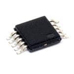
| 描述 | IC DAC NANO 16BIT QUAD 10-MSOP数模转换器- DAC Quad 16-Bit IC RRO 4uS |
| 产品分类 | |
| 品牌 | Analog Devices |
| 产品手册 | |
| 产品图片 |
|
| rohs | 符合RoHS无铅 / 符合限制有害物质指令(RoHS)规范要求 |
| 产品系列 | 数据转换器IC,数模转换器- DAC,Analog Devices AD5664BRMZnanoDAC™ |
| 数据手册 | |
| 产品型号 | AD5664BRMZ |
| 产品培训模块 | http://www.digikey.cn/PTM/IndividualPTM.page?site=cn&lang=zhs&ptm=19145http://www.digikey.cn/PTM/IndividualPTM.page?site=cn&lang=zhs&ptm=18614http://www.digikey.cn/PTM/IndividualPTM.page?site=cn&lang=zhs&ptm=26125http://www.digikey.cn/PTM/IndividualPTM.page?site=cn&lang=zhs&ptm=26140http://www.digikey.cn/PTM/IndividualPTM.page?site=cn&lang=zhs&ptm=26150http://www.digikey.cn/PTM/IndividualPTM.page?site=cn&lang=zhs&ptm=26147 |
| 产品目录页面 | |
| 产品种类 | 数模转换器- DAC |
| 位数 | 16 |
| 供应商器件封装 | 10-MSOP |
| 分辨率 | 16 bit |
| 包装 | 管件 |
| 商标 | Analog Devices |
| 安装类型 | 表面贴装 |
| 安装风格 | SMD/SMT |
| 封装 | Tube |
| 封装/外壳 | 10-TFSOP,10-MSOP(0.118",3.00mm 宽) |
| 封装/箱体 | MSOP-10 |
| 工作温度 | -40°C ~ 105°C |
| 工厂包装数量 | 50 |
| 建立时间 | 4µs |
| 接口类型 | SPI |
| 数据接口 | DSP,MICROWIRE™,QSPI™,串行,SPI™ |
| 最大功率耗散 | 4.5 mW |
| 最大工作温度 | + 105 C |
| 最小工作温度 | - 40 C |
| 标准包装 | 50 |
| 电压参考 | External |
| 电压源 | 单电源 |
| 电源电压-最大 | 5.5 V |
| 电源电压-最小 | 2.7 V |
| 积分非线性 | +/- 12 LSB |
| 稳定时间 | 4 us |
| 系列 | AD5664 |
| 结构 | Resistor String |
| 转换器数 | 4 |
| 转换器数量 | 4 |
| 输出数和类型 | 4 电压,单极4 电压,双极 |
| 输出类型 | Voltage |
| 配用 | /product-detail/zh/EVAL-AD5664REBZ/EVAL-AD5664REBZ-ND/1679963 |
| 采样比 | 223 kSPs |
| 采样率(每秒) | 223k |


- 商务部:美国ITC正式对集成电路等产品启动337调查
- 曝三星4nm工艺存在良率问题 高通将骁龙8 Gen1或转产台积电
- 太阳诱电将投资9.5亿元在常州建新厂生产MLCC 预计2023年完工
- 英特尔发布欧洲新工厂建设计划 深化IDM 2.0 战略
- 台积电先进制程称霸业界 有大客户加持明年业绩稳了
- 达到5530亿美元!SIA预计今年全球半导体销售额将创下新高
- 英特尔拟将自动驾驶子公司Mobileye上市 估值或超500亿美元
- 三星加码芯片和SET,合并消费电子和移动部门,撤换高东真等 CEO
- 三星电子宣布重大人事变动 还合并消费电子和移动部门
- 海关总署:前11个月进口集成电路产品价值2.52万亿元 增长14.8%


PDF Datasheet 数据手册内容提取
2.7 V to 5.5 V, 450 μA, Rail-to-Rail Output, Quad, 12-/16-Bit nanoDACs Data Sheet AD5624/AD5664 FEATURES FUNCTIONAL BLOCK DIAGRAM Low power, quad nanoDACs VDD GND VREF AD5664: 16 bits AD5624/AD5664 AD5624: 12 bits Relative accuracy: ±12 LSBs max REINGPISUTTER REGDIASCTER SDTARCIN AG BUFFER VOUTA SCLK Guaranteed monotonic by design 10-lead MSOP and 3 mm × 3 mm LFCSP_WD INTLEORGFIACCE REINGPISUTTER REGDIASCTER SDTARCIN BG BUFFER VOUTB SYNC 2.7 V to 5.5 V power supply Power-on reset to zero REINGPISUTTER REGDIASCTER SDTARCIN CG BUFFER VOUTC DIN Per channel power-down REINGPISUTTER REGDIASCTER SDTARCIN DG BUFFER VOUTD Serial interface, up to 50 MHz APPLICATIONS PORWEESRE-TON POWLEORG-DICOWN 05943-001 Figure 1. Process control Data acquisition systems Portable battery-powered instruments Digital gain and offset adjustment Programmable voltage and current sources Programmable attenuators GENERAL DESCRIPTION The AD5624/AD5664, members of the nanoDAC® family, are The AD5624/AD5664 use a versatile 3-wire serial interface that low power, quad, 12-, 16-bit buffered voltage-out DACs that operates at clock rates up to 50 MHz, and are compatible with operate from a single 2.7 V to 5.5 V supply and are guaranteed standard SPI®, QSPI™, MICROWIRE™, and DSP interface monotonic by design. standards. PRODUCT HIGHLIGHTS The AD5624/AD5664 require an external reference voltage to set the output range of the DAC. The device incorporates a 1. Relative accuracy: ±12 LSBs maximum. power-on reset circuit that ensures the DAC output powers up 2. Available in 10-lead MSOP and 10-lead, 3 mm × 3 mm, to 0 V and remains there until a valid write takes place. The LFCSP_WD. devices contain a power-down feature that reduces the current 3. Low power, typically consumes 1.32 mW at 3 V and consumption of the device to 480 nA at 5 V and provides 2.25 mW at 5 V. software-selectable output loads while in power-down mode. 4. Maximum settling time of 4.5 μs (AD5624) and 7 μs (AD5664). The low power consumption of these devices in normal operation makes them ideally suited to portable battery- operated equipment. The power consumption is 2.25 mW at 5 Table 1. Related Devices V, going down to 2.4 μW in power-down mode. Part No. Description AD5624R/AD5644R/AD5664R 2.7 V to 5.5 V quad, 12-, 14-, The AD5624/AD5664 on-chip precision output amplifier allows 16-bit DACs with internal rail-to-rail output swing to be achieved. reference Rev. A Document Feedback Information furnished by Analog Devices is believed to be accurate and reliable. However, no responsibility is assumed by Analog Devices for its use, nor for any infringements of patents or other One Technology Way, P.O. Box 9106, Norwood, MA 02062-9106, U.S.A. rights of third parties that may result from its use. Specifications subject to change without notice. No license is granted by implication or otherwise under any patent or patent rights of Analog Devices. Tel: 781.329.4700 ©2006–2018 Analog Devices, Inc. All rights reserved. Trademarks and registered trademarks are the property of their respective owners. Technical Support www.analog.com
AD5624/AD5664 Data Sheet TABLE OF CONTENTS Features .............................................................................................. 1 Serial Interface ............................................................................ 15 Applications ....................................................................................... 1 Input Shift Register .................................................................... 16 Functional Block Diagram .............................................................. 1 SYNC Interrupt .......................................................................... 16 General Description ......................................................................... 1 Power-On Reset .......................................................................... 16 Product Highlights ........................................................................... 1 Software Reset ............................................................................. 17 Revision History ............................................................................... 2 Power-Down Modes .................................................................. 17 Specifications ..................................................................................... 3 LDAC Function .......................................................................... 18 AC Characteristics ........................................................................ 4 Microprocessor Interfacing ....................................................... 19 Timing Characteristics ................................................................ 5 Applications Information .............................................................. 20 Timing Diagram ........................................................................... 5 Choosing a Reference for the AD5624/AD5664 ........................ 20 Absolute Maximum Ratings ............................................................ 6 Using a Reference as a Power Supply for the AD5624/AD5664 ........................................................................ 20 ESD Caution .................................................................................. 6 Bipolar Operation Using the AD5624/AD5664 ......................... 21 Pin Configuration and Function Descriptions ............................. 7 Using AD5624/AD5664 with a Galvanically Isolated Typical Performance Characteristics ............................................. 8 Interface ....................................................................................... 21 Terminology .................................................................................... 13 Power Supply Bypassing and Grounding ................................ 21 Theory of Operation ...................................................................... 15 Outline Dimensions ....................................................................... 22 D/A Section ................................................................................. 15 Ordering Guide ............................................................................... 23 Resistor String ............................................................................. 15 Output Amplifier ........................................................................ 15 REVISION HISTORY 6/2018—Rev. 0 to Rev. A Changes to Figure 3 Caption and Table 6 ...................................... 7 Add Figure 4; Renumber Sequentially ........................................... 7 Changed Applications Section to Applications Information Section .............................................................................................. 20 Updated Outline Dimensions ....................................................... 22 Changes to Ordering Guide .......................................................... 23 6/2006—Revision 0: Initial Version Rev. A | Page 2 of 23
Data Sheet AD5624/AD5664 SPECIFICATIONS V = +2.7 V to +5.5 V; R = 2 kΩ to GND; C = 200 pF to GND; V = V ; all specifications T to T , unless otherwise noted. DD L L REF DD MIN MAX Table 2. AGrade1 B Grade1 Parameter Min Typ Max Min Typ Max Unit Conditions/Comments STATIC PERFORMANCE2 AD5664 Resolution 16 16 Bits Relative Accuracy ±8 ±16 ±6 ±12 LSB Differential Nonlinearity ±1 ±1 LSB Guaranteed monotonic by design AD5624 Resolution 12 Bits Relative Accuracy ±0.5 ±1 LSB Differential Nonlinearity ±0.25 LSB Guaranteed monotonic by design Zero Code Error 2 10 2 10 mV All zeroes loaded to DAC register Offset Error ±1 ±10 ±1 ±10 mV Full-Scale Error −0.1 ±1 −0.1 ±1 % of FSR All ones loaded to DAC register Gain Error ±1.5 ±1.5 % of FSR Zero Code Error Drift ±2 ±2 μV/°C Gain Temperature ±2.5 ±2.5 ppm Of FSR/°C Coefficient DC Power Supply Rejection −100 −100 dB DAC code = midscale ; V ± 10% DD Ratio DC Crosstalk 10 10 μV Due to full-scale output change R = 2 kΩ to GND or V L DD 10 10 μV/mA Due to load current change 5 5 μV Due to powering down (per channel) OUTPUT CHARACTERISTICS3 Output Voltage Range 0 V 0 V V DD DD Capacitive Load Stability 2 2 nF R = ∞ L 10 10 nF R = 2 kΩ L DC Output Impedance 0.5 0.5 Ω Short-Circuit Current 30 30 mA V = 5 V DD Power-Up Time 4 4 μs Coming out of power-down mode; V = 5 V DD REFERENCE INPUTS Reference Current 170 200 170 200 μA V = V = 5.5 V REF DD Reference Input Range 0.75 V 0.75 V V DD DD Reference Input Impedance 26 26 kΩ LOGIC INPUTS3 Input Current ±2 ±2 μA All digital inputs V , Input Low Voltage 0.8 0.8 V V = 5 V, 3 V INL DD V , Input High Voltage 2 2 V V = 5 V, 3 V INH DD Pin Capacitance 3 3 pF Rev. A | Page 3 of 23
AD5624/AD5664 Data Sheet AGrade1 B Grade1 Parameter Min Typ Max Min Typ Max Unit Conditions/Comments POWER REQUIREMENTS V 2.7 5.5 2.7 5.5 V DD I (Normal Mode)4 V = V , V = GND DD IH DD IL V = 4.5 V to 5.5 V 0.45 0.9 0.45 0.9 mA DD V = 2.7 V to 3.6 V 0.44 0.85 0.44 0.85 mA DD I (All Power-Down V = V , V = GND DD IH DD IL Modes)5 V = 4.5 V to 5.5 V 0.48 1 0.48 1 μA DD V = 2.7 V to 3.6 V 0.2 1 0.2 1 μA DD 1 Temperature range: A grade and B grade: −40°C to +105°C. 2 Linearity calculated using a reduced code range: AD5664 (Code 512 to Code 65,024); AD5624 (Code 32 to Code 4064); output unloaded. 3 Guaranteed by design and characterization, not production tested. 4 Interface inactive. All DACs active. DAC outputs unloaded. 5 All DACs powered down. AC CHARACTERISTICS V = 2.7 V to 5.5 V; R = 2 kΩ to GND; C = 200 pF to GND; V = V ; all specifications T to T , unless otherwise noted.1 DD L L REF DD MIN MAX Table 3. Parameter2, 3 Min Typ Max Unit Conditions/Comments Output Voltage Settling Time AD5664 4 7 μs ¼ to ¾ scale settling to ±2 LSB AD5624 3 4.5 μs ¼ to ¾ scale settling to ±0.5 LSB Slew Rate 1.8 V/μs Digital-to-Analog Glitch Impulse 10 nV-s 1 LSB change around major carry Digital Feedthrough 0.1 nV-s Reference Feedthrough −90 dBs V = 2 V ± 0.1 V p-p, frequency 10 Hz to 20 MHz REF Digital Crosstalk 0.1 nV-s Analog Crosstalk 1 nV-s DAC-to-DAC Crosstalk 1 nV-s Multiplying Bandwidth 340 kHz V = 2 V ± 0.1 V p-p REF Total Harmonic Distortion −80 dB V = 2 V ± 0.1 V p-p, frequency = 10 kHz REF Output Noise Spectral Density 120 nV/√Hz DAC code = midscale, 1 kHz 100 nV/√Hz DAC code = midscale, 10 kHz Output Noise 15 μV p-p 0.1 Hz to 10 Hz 1 Guaranteed by design and characterization, not production tested. 2 Temperature range: −40°C to +105°C; typical at 25°C. 3 See the Terminology section. Rev. A | Page 4 of 23
Data Sheet AD5624/AD5664 TIMING CHARACTERISTICS All input signals are specified with t = t = 1 ns/V (10% to 90% of V ) and timed from a voltage level of (V + V )/2 (see Figure 2). R F DD IL IH V = 2.7 V to 5.5 V; all specifications T to T , unless otherwise noted. DD MIN MAX Table 4. Limit atT , T MIN MAX Parameter1 V = 2.7 V to 5.5 V Unit Conditions/Comments DD t2 20 ns min SCLK cycle time 1 t 9 ns min SCLK high time 2 t 9 ns min SCLK low time 3 t 13 ns min SYNC to SCLK falling edge setup time 4 t 5 ns min Data setup time 5 t 5 ns min Data hold time 6 t 0 ns min SCLK falling edge to SYNC rising edge 7 t 15 ns min Minimum SYNC high time 8 t 13 ns min SYNC rising edge to SCLK fall ignore 9 t 0 nsmin SCLK falling edge to SYNC fall ignore 10 1 Guaranteed by design and characterization, not production tested. 2 Maximum SCLK frequency is 50 MHz at VDD = 2.7 V to 5.5 V. TIMING DIAGRAM t10 t1 t 9 SCLK t t8 t t3 2 t7 4 SYNC t 6 t 5 DIN DB23 DB0 05943-002 Figure 2. Serial Write Operation Rev. A | Page 5 of 23
AD5624/AD5664 Data Sheet ABSOLUTE MAXIMUM RATINGS T = 25°C, unless otherwise noted. Stresses at or above those listed under Absolute Maximum A Ratings may cause permanent damage to the product. This is a Table 5. stress rating only; functional operation of the product at these Parameter Rating or any other conditions above those indicated in the operational V to GND −0.3 V to +7 V section of this specification is not implied. Operation beyond DD V to GND −0.3 V to V + 0.3 V the maximum operating conditions for extended periods may OUT DD V to GND −0.3 V to V + 0.3 V affect product reliability. REF DD Digital Input Voltage to GND −0.3 V to V + 0.3 V DD ESD CAUTION Operating Temperature Range Industrial (A Grade, B Grade) −40°C to +105°C Storage Temperature Range −65°C to +150°C Junction Temperature (T max) 150°C J Power Dissipation (T max − T )/θ J A JA LFCSP_WD Package (4-Layer Board) θ Thermal Impedance 61°C/W JA MSOP Package (4-Layer Board) θ Thermal Impedance 142°C/W JA θ Thermal Impedance 43.7°C/W JC Reflow Soldering Peak Temperature Pb-Free 260°C ± 5°C Rev. A | Page 6 of 23
Data Sheet AD5624/AD5664 PIN CONFIGURATION AND FUNCTION DESCRIPTIONS VOUTA1 10 VREF VOUTB2 AD5624/ 9 VDD GND3 AD5664 8 DIN TOP VIEW VOUTA 1 10 VREF VOUTC4 (Not to Scale) 7 SCLK VOUTB 2 AADD55662644/ 9 VDD VOUTD5 6 SYNC GND 3 8 DIN TOP VIEW VVOOUUTTCD 45 (Not to Scale) 76 SSCYNLKC 05943-003 N1 . O EOTXNEP SLOFSCESDPPPAADC KTAIEGDET.O GND 05943-104 Figure 3. 10-Lead MSOP Pin Configuration Figure 4. 10-Lead LFCSP Pin Configuration Table 6. Pin Function Descriptions Pin No. Mnemonic Description 1 V A Analog Output Voltage from DAC A. The output amplifier has rail-to-rail operation. OUT 2 V B Analog Output Voltage from DAC B. The output amplifier has rail-to-rail operation. OUT 3 GND Ground Reference Point for All Circuitry on the device 4 V C Analog Output Voltage from DAC C. The output amplifier has rail-to-rail operation. OUT 5 V D Analog Output Voltage from DAC D. The output amplifier has rail-to-rail operation. OUT 6 SYNC Active Low Control Input. This is the frame synchronization signal for the input data. When SYNC goes low, it powers on the SCLK and DIN buffers and enables the input shift register. Data is transferred in on the falling edges of the next 24 clocks. If SYNC is taken high before the 24th falling edge, the rising edge of SYNC acts as an interrupt and the write sequence is ignored by the device. 7 SCLK Serial Clock Input. Data is clocked into the input shift register on the falling edge of the serial clock input. Data can be transferred at rates up to 50 MHz. 8 DIN Serial Data Input. This device has a 24-bit input shift register. Data is clocked into the register on the falling edge of the serial clock input. 9 V Power Supply Input. These devices can be operated from 2.7 V to 5.5 V. The supply is decoupled with a 10 μF DD capacitor in parallel with a 0.1 μF capacitor to GND. 10 V Reference Voltage Input. REF EPAD Exposed Pad. Exposed pad tied to GND on LFCSP package. Rev. A | Page 7 of 23
AD5624/AD5664 Data Sheet TYPICAL PERFORMANCE CHARACTERISTICS 10 0.20 8 TVAD D= =2 5V°RCEF = 5V 0.15 TVAD D= =2 5V°RCEF = 5V 6 0.10 4 INL ERROR (LSB) ––2402 DNL ERROR (LSB) –00..00550 –0.10 –6 –1–08 05943-004 ––00..2105 05943-007 0 5k 10k 15k 20k 25k 30k 35k 40k 45k 50k 55k 60k 65k 0 500 1000 1500 2000 2500 3000 3500 4000 CODE CODE Figure 5. INL AD5664 Figure 8. DNL AD5624 1.0 8 VDD = VREF = 5V 0.8 TA = 25°C 6 MAX INL 0.6 VDD = VREF = 5V 4 0.4 OR (LSB) 0.02 R (LSB) 20 MAX DNL R O L ER –0.2 ERR –2 MIN DNL N I –0.4 –4 –0.6 MIN INL ––10..08 05943-005 ––68 05856-022 0 500 1000 1500 2000 2500 3000 3500 4000 –40 –20 0 20 40 60 80 100 CODE TEMPERATURE (°C) Figure 6. INL AD5624 Figure 9. INL Error and DNL Error vs. Temperature 1.0 10 VDD = VREF = 5V 0.8 TA = 25°C 8 MAX INL 0.6 6 VDD = 5V B) 0.4 4 TA = 25°C LS 0.2 B) 2 R ( LS MAX DNL RO 0 R ( 0 R O NL E –0.2 ERR –2 MIN DNL D –0.4 –4 –0.6 –6 MIN INL ––10..08 05943-006 –1–08 05943-009 0 10k 20k 30k 40k 50k 60k 0.75 1.25 1.75 2.25 2.75 3.25 3.75 4.25 4.75 CODE VREF (V) Figure 7. DNL AD5664 Figure 10. INL and DNL Error vs. VREF Rev. A | Page 8 of 23
Data Sheet AD5624/AD5664 8 1.0 6 MAX INL TA = 25°C 0.5 4 GAIN ERROR B) 2 SR) 0 OR (LS 0 MAX DNL R (% F –0.5 FULL-SCALE ERROR RR MIN DNL RO E –2 R E –1.0 –4 MIN INL –1.5 ––68 05943-010 –2.0 05943-013 2.7 3.2 3.7 4.2 4.7 5.2 2.7 3.2 3.7 4.2 4.7 5.2 VDD (V) VDD (V) Figure 11. INL and DNL Error vs. Supply Figure 14. Gain Error and Full-Scale Error vs. Supply 0 1.0 VDD = 5V TA = 25°C –0.02 0.5 ZERO-SCALE ERROR –0.04 GAIN ERROR –0.06 0 SR) –0.08 V) F m –0.5 R (% –0.10 OR ( RRO –0.12 ERR –1.0 E –0.14 FULL-SCALE ERROR –1.5 –0.16 ––00..1280 05943-011 ––22..05 OFFSET ERROR 05943-014 –40 –20 0 20 40 60 80 100 2.7 3.2 3.7 4.2 4.7 5.2 TEMPERATURE (°C) VDD (V) Figure 12. Gain Error and Full-Scale Error vs. Temperature Figure 15. Zero-Scale Error and Offset Error vs. Supply 1.5 VDD= 5.5V 1.0 ZERO-SCALE ERROR 6 TA = 25°C 0.5 5 RROR (mV) –0.50 REQUENCY 34 E –1.0 F 2 –1.5 OFFSET ERROR 1 ––22..05 05943-012 0 05943-017 –40 –20 0 20 40 60 80 100 0.41 0.42 0.43 0.44 0.45 TEMPERATURE (°C) IDD (mA) Figure 13. Zero-Scale Error and Offset Error vs. Temperature Figure 16. IDD Histogram with VDD = 5.5 V Rev. A | Page 9 of 23
AD5624/AD5664 Data Sheet 8 VDD= 3.6V TA = 25°C 7 6 VDD = VREF = 5V NCY 5 FTUA L=L 2-S5°CCALE CODE CHANGE E 0x0000TO 0xFFFF QU 4 OUTPUT LOADED WITH 2kΩ RE AND 200pFTO GND F 3 2 VOUT= 909mV/DIV 1 01 0.39 0.40 0.41 0.42 0.43 05943-018 05943-021 TIME BASE = 4µs/DIV IDD (mA) Figure 17. IDD Histogram with VDD = 3.6 V Figure 20. Full-Scale Settling Time, 5 V 0.20 0.15 VTAD D= =2 5V°RCEF= 5V, 3V DZSEIANRCKO ILN OSGCA ACDLUEERD R –WEINTTH VTAD D= =2 5V°RCEF = 5V 0.10 E (V) 0.05 G TA 0 L O R V –0.05 VDD RO 1 R –0.10 E –0.15 MAX(C2) DAC LOADED WITH 420.0mV ––00..2250 FSUOLULR SCCINAGL EC U–RRENT 05943-016 2 VOUT 05943-022 –5 –4 –3 –2 –1 0 1 2 3 4 5 CH1 2.0V CH2 500mV M100µs 125MS/s 8.0ns/pt I (mA) A CH1 1.28V Figure 18. Headroom at Rails vs. Source and Sink Current Figure 21. Power-On Reset to 0 V 0.50 VDD = VREFIN = 5V 0.45 SYNC 0.40 VDD = VREFIN = 3V 1 SLCK 0.35 3 0.30 A) (mD 0.25 D I 0.20 0.15 0.10 VOUT VDD = 5V 0.050–40TA = 2–52°0C 0 TEM2P0ERATU4R0E (°C)60 80 100 05943-026 2 CCHH13 55..00VV CH2 500mV M400ns A CH1 1.4V 05943-023 Figure 19. Supply Current vs. Temperature Figure 22. Exiting Power-Down to Midscale Rev. A | Page 10 of 23
Data Sheet AD5624/AD5664 2.538 16 22..553367 5VTnADs D=/S =2A 5VM°RCPEFL E= 5NVUMBER VTAR E=F 2=5 °VCDD 2.535 GLITCH IMPULSE = 9.494nV 14 2.534 1LSB CHANGEAROUND 2.533 MIDSCALE (0x8000TO 0x7FFF) VDD=3V 2.532 12 (V)OUT222...555233901 ME (µs) 10 V 2.528 TI 2.527 8 VDD=5V 2.526 2.525 2.524 6 222...555222123 05943-024 4 05943-028 0 50 100 150 200 250 300 350 400 450 512 0 1 2 3 4 5 6 7 8 9 10 SAMPLE NUMBER CAPACITANCE (nF) Figure 23. Digital-to-Analog Glitch Impulse (Negative) Figure 26. Settling Time vs. Capacitive Load 2.498 VDD= VREF = 5V TA = 25°C 2.497 5ns/SAMPLE NUMBER ANALOG CROSSTALK = 0.424nV VDD = VREF = 5V TA = 25°C 2.496 DAC LOADED WITH MIDSCALE V) 2.495 (UT O V 2.494 1 2.493 2.492 2.4910 50 100 150 S2A0M0PL2E5 0NUM30B0ER350 400 450 51205943-025 YXAAXXIISS == 24µsV/D/DIVIV 05943-029 Figure 24. Analog Crosstalk Figure 27. 0.1 Hz to 10 Hz Output Noise Plot –20 800 VDD = 5V VDD = VREF = 5V –30 TDAA C= 2L5O°ACDED WITH FULL SCALE 700 TA = 25°C VREF = 2V ± 0.3V p-p –40 Hz) 600 –50 nV/√ 500 (dB) –60 NOISE ( 400 T –70 PU 300 T U –80 O 200 –1–0900 2k 4k 6k 8k 10k05943-027 100010 100 1k 10k 100k 1M05943-030 (Hz) FREQUENCY (Hz) Figure 25. Total Harmonic Distortion Figure 28. Noise Spectral Density Rev. A | Page 11 of 23
AD5624/AD5664 Data Sheet 5 VDD = 5V 0 TA = 25°C –5 –10 –15 B) d ( –20 –25 –30 ––4305 05943-031 10k 100k 1M 10M FREQUENCY (Hz) Figure 29. Multiplying Bandwidth Rev. A | Page 12 of 23
Data Sheet AD5624/AD5664 TERMINOLOGY Relative Accuracy or Integral Nonlinearity (INL) DC Power Supply Rejection Ratio (PSRR) For the DAC, relative accuracy or integral nonlinearity is a This indicates how the output of the DAC is affected by changes measurement of the maximum deviation, in LSBs, from a straight in the supply voltage. PSRR is the ratio of the change in V to OUT line passing through the endpoints of the DAC transfer function. A a change in V for full-scale output of the DAC. It is measured DD typical INL vs. code plot can be seen in Figure 5 and Figure 6. in dB. V is held at 2 V, and V is varied by ±10%. REF DD Differential Nonlinearity (DNL) Output Voltage Settling Time Differential nonlinearity is the difference between the measured This is the amount of time it takes for the output of a DAC to change and the ideal 1 LSB change between any two adjacent settle to a specified level for a ¼ to ¾ full-scale input change and is codes. A specified differential nonlinearity of ±1 LSB maximum measured from the 24th falling edge of SCLK. ensures monotonicity. This DAC is guaranteed monotonic by Digital-to-Analog Glitch Impulse design. A typical DNL vs. code plot can be seen in Figure 7 and Digital-to-analog glitch impulse is the impulse injected into the Figure 8. analog output when the input code in the DAC register changes Zero-Scale Error state. It is normally specified as the area of the glitch in nV-s, Zero-scale error is a measurement of the output error when and is measured when the digital input code is changed by 1 LSB at zero code (0x0000) is loaded to the DAC register. Ideally, the the major carry transition (0x7FFF to 0x8000) as shown in output is 0 V. The zero code error is always positive in the Figure 23. AD5624/AD5664 because the output of the DAC cannot go Digital Feedthrough below 0 V. It is due to a combination of the offset errors in the Digital feedthrough is a measure of the impulse injected into DAC and the output amplifier. Zero code error is expressed in the analog output of the DAC from the digital inputs of the mV. A plot of zero code error vs. temperature can be seen in DAC, but is measured when the DAC output is not updated. It Figure 13. is specified in nV-s, and measured with a full-scale code change Full-Scale Error on the data bus, that is, from all 0s to all 1s and vice versa. Full-scale error is a measurement of the output error when full- Total Harmonic Distortion (THD) scale code (0xFFFF) is loaded to the DAC register. Ideally, the This is the difference between an ideal sine wave and its attenuated output is V − 1 LSB. Full-scale error is expressed in % of FSR. DD version using the DAC. The sine wave is used as the reference A plot of full-scale error vs. temperature can be seen in Figure 12. for the DAC, and the THD is a measurement of the harmonics Gain Error present on the DAC output. It is measured in dB. This is a measure of the span error of the DAC. It is the deviation in Noise Spectral Density slope of the DAC transfer characteristic from ideal expressed as This is a measurement of the internally generated random noise. a % of FSR. Random noise is characterized as a spectral density (nV/√Hz). Zero Code Error Drift It is measured by loading the DAC to midscale and measuring This is a measurement of the change in zero code error with a noise at the output. It is measured in nV/√Hz. A plot of noise change in temperature. It is expressed in μV/°C. spectral density can be seen in Figure 28. Gain Temperature Coefficient DC Crosstalk This is a measurement of the change in gain error with changes DC crosstalk is the dc change in the output level of one DAC in in temperature. It is expressed in ppm of FSR/°C. response to a change in the output of another DAC. It is measured with a full-scale output change on one DAC (or soft power-down Offset Error and power-up) while monitoring another DAC kept at midscale. Offset error is a measure of the difference between V (actual) OUT It is expressed in μV. and V (ideal) expressed in mV in the linear region of the OUT DC crosstalk due to load current change is a measure of the transfer function. Offset error is measured on the AD5624/ impact that a change in load current on one DAC has to another AD5664 with code 512 loaded in the DAC register. It can be DAC kept at midscale. It is expressed in μV/mA. negative or positive. Rev. A | Page 13 of 23
AD5624/AD5664 Data Sheet Digital Crosstalk DAC-to-DAC Crosstalk This is the glitch impulse transferred to the output of one DAC This is the glitch impulse transferred to the output of one DAC due to a digital code change and subsequent analog output change at midscale in response to a full-scale code change (all 0s to all of another DAC. It is measured by loading the attack channel 1s and vice versa) in the input register of another DAC. It is with a full-scale code change (all 0s to all 1s and vice versa) using measured in standalone mode and is expressed in nV-s. the command write to and update while monitoring the output of Analog Crosstalk the victim channel that is at midscale. The energy of the glitch is This is the glitch impulse transferred to the output of one DAC expressed in nV-s. due to a change in the output of another DAC. It is measured by Multiplying Bandwidth loading one of the input registers with a full-scale code change The amplifiers within the DAC have a finite bandwidth. The (all 0s to all 1s and vice versa). Then execute a software LDAC multiplying bandwidth is a measure of this. A sine wave on the and monitor the output of the DAC whose digital code was reference (with full-scale code loaded to the DAC) appears on not changed. The area of the glitch is expressed in nV-s (see the output. The multiplying bandwidth is the frequency at which Figure 24). the output amplitude falls to 3 dB below the input. Rev. A | Page 14 of 23
Data Sheet AD5624/AD5664 THEORY OF OPERATION D/A SECTION R The AD5624/AD5664 DACs are fabricated on a CMOS process. The architecture consists of a string DAC followed by an output R buffer amplifier. Figure 30 shows a block diagram of the DAC architecture. R TO OUTPUT VDD OUTPUT AMPLIFIER AMPLIFIER (GAIN = +2) REF (+) REGDIASCTER RSETSRISINTOGR VOUT REF (–) GND 05943-032 R Figure 30. DAC Architecture R Soiuntcpeu tt hveo litnapguet i sc ogdivineng btoy the DAC is straight binary, the ideal 05943-033 Figure 31. Resistor String D VOUT VREFIN 2N SERIAL INTERFACE The AD5624/AD5664 have a 3-wire serial interface (SYNC, where: SCLK, and DIN) that is compatible with SPI, QSPI, and D is the decimal equivalent of the binary code that is loaded to MICROWIRE interface standards as well as with most DSPs. the DAC register: See Figure 2 for a timing diagram of a typical write sequence. 0 to 4095 for AD5624 (12 bit). The write sequence begins by bringing the SYNC line low. Data 0 to 65535 for AD5664 (16 bit). from the DIN line is clocked into the 24-bit shift register on the N is the DAC resolution. falling edge of SCLK. The serial clock frequency can be as high as 50 MHz, making the AD5624/AD5664 compatible with high RESISTOR STRING speed DSPs. On the 24th falling clock edge, the last data bit is The resistor string is shown in Figure 31. It is simply a string of clocked in and the programmed function is executed, that is, a resistors, each of value R. The code loaded to the DAC register change in DAC register contents and/or a change in the mode determines at which node on the string the voltage is tapped off of operation. At this stage, the SYNC line can be kept low or be to be fed into the output amplifier. The voltage is tapped off by brought high. In either case, it must be brought high for a closing one of the switches connecting the string to the amplifier. minimum of 15 ns before the next write sequence so that a falling Because it is a string of resistors, it is guaranteed monotonic. edge of SYNC can initiate the next write sequence. Because the OUTPUT AMPLIFIER SYNC buffer draws more current when VIN = 2.0 V than it does when V = 0.8 V, SYNC is idled low between write sequences for IN The output buffer amplifier can generate rail-to-rail voltages on even lower power operation. It must, however, be brought high its output, which gives an output range of 0 V to VDD. It can again just before the next write sequence. drive a load of 2 kΩ in parallel with 1000 pF to GND. The source and sink capabilities of the output amplifier can be seen in Figure 18. The slew rate is 1.8 V/μs with a ¼ to ¾ full-scale settling time of 7 μs. Rev. A | Page 15 of 23
AD5624/AD5664 Data Sheet INPUT SHIFT REGISTER SYNC INTERRUPT The input shift register is 24 bits wide. The first two bits are don’t In a normal write sequence, the SYNC line is kept low for at least care bits. The next three bits are the Command bits, C2 to C0 24 falling edges of SCLK, and the DAC is updated on the 24th (see Table 7), followed by the 3-bit DAC address, A2 to A0 (see falling edge. However, if SYNC is brought high before the 24th Table 8), and then the 16-, 12-bit data-word. The data-word falling edge, then this acts as an interrupt to the write sequence. comprises the 16-, 12- bit input code followed by 0 or 4 don’t The input shift register is reset and the write sequence is seen as care bits for the AD5664 and AD5624 respectively (see Figure 32 invalid. Neither an update of the DAC register contents nor a and Figure 33). These data bits are transferred to the DAC change in the operating mode occurs (see Figure 34). register on the 24th falling edge of SCLK. POWER-ON RESET Table 7. Command Definition The AD5624/AD5664 family contains a power-on reset circuit C2 C1 C0 Command that controls the output voltage during power-up. The AD5624/ 0 0 0 Write to input register n AD5664 DAC outputs power up to 0 V and the output remains 0 0 1 Update DAC register n there until a valid write sequence is made to the DAC. This is 0 1 0 Write to input register n, update all (software useful in applications where it is important to know the state of LDAC) the output of the DAC while it is in the process of powering up. 0 1 1 Write to and update DAC channel n 1 0 0 Power down DAC (power-up) 1 0 1 Reset 1 1 0 Load LDAC register 1 1 1 Reserved Table 8. Address Command A2 A1 A0 ADDRESS (n) 0 0 0 DAC A 0 0 1 DAC B 0 1 0 DAC C 0 1 1 DAC D 1 1 1 All DACs DB23 (MSB) DB0 (LSB) X X C2 C1 C0 A2 A1 A0 D15 D14 D13 D12 D11 D10 D9 D8 D7 D6 D5 D4 D3 D2 D1 D0 COMMAND BITS ADDRESS BITS DATA BITS 05943-034 Figure 32. AD5664 Input Shift Register Contents DB23 (MSB) DB0 (LSB) X X C2 C1 C0 A2 A1 A0 D11 D10 D9 D8 D7 D6 D5 D4 D3 D2 D1 D0 X X X X COMMAND BITS ADDRESS BITS DATA BITS 05943-035 Figure 33. AD5624 Input Shift Register Contents SCLK SYNC DIN DB23 DB0 DB23 DB0 SYNC HINIGVHA LBIDEF WORRIET E2 4STEHQ FUAELNLCINEG: EDGE VALID WORNIT TEH SEE 2Q4UTEH NFCAEL,L OINUGT PEUDTG UEPDATES 05943-036 Figure 34. SYNC Interrupt Facility Rev. A | Page 16 of 23
Data Sheet AD5624/AD5664 SOFTWARE RESET Table 10. Modes of Operation for the AD5624/AD5664 DB5 DB4 Operating Mode The AD5624/AD5664 contain a software reset function. 0 0 Normal operation Command 110 is reserved for the software reset function (see Power-down modes Table 7). The software reset command contains two reset modes 0 1 1 kΩ to GND that are software programmable by setting Bit DB0 in the control 1 0 100 kΩ to GND register. Table 9 shows how the state of the bit corresponds to 1 1 Three-state the software reset modes of operation of the devices. When both bits are set to 0, the devices work normally with Table 9. Software Reset Modes for the AD5624/AD5664 their normal power consumption of 450 μA at 5 V. However, for DB0 Registers Reset to Zero the three power-down modes, the supply current falls to 480 nA 0 DACregister at 5 V (200 nA at 3 V). Not only does the supply current fall, but Input shift register the output stage is also internally switched from the output of 1 (Power-On Reset) DAC register the amplifier to a resistor network of known values. This allows Input shift register the output impedance of the device to be known while the LDACregister device is in power-down mode. Power-downregister The outputs can either be connected internally to GND through POWER-DOWN MODES a 1 kΩ or 100 kΩ resistor, or left open circuited (three-state) The AD5624/AD5664 contain four separate modes of operation. (see Figure 35). Command 100 is reserved for the power-down function (see Table 7). These modes are software programmable by setting two bits (DB5 and DB4) in the control register. Table 10 shows how SRTERSINISGT DOARC AMPLIFIER VOUT the state of the bits corresponds to the mode of operation of the device. All DACs (DAC D to DAC A) can be powered down to the selected mode by setting the corresponding four bits (DB3, POWER-DOWN DB2, DB1, and DB0) to 1. By executing the same Command 100, CIRCUITRY RESISTOR aBnity D coBm4 btoin naotiromna ol fo DpeArCatsi oisn p mowodeere. dT ou pse bleyc ts ewtthinicgh B ciot mDbBi5n aatniodn NETWORK 05943-037 Figure 35. Output Stage During Power-Down of DAC channels to power-up, set the corresponding four bits (DB3, DB2, DB1, and DB0) to 1. See Table 11 for contents of the The bias generator, the output amplifier, the resistor string, and input shift register during the power-down/power-up operation. other associated linear circuitry are shut down when power-down mode is activated. However, the contents of the DAC register are unaffected when in power-down. The time to exit power-down is typically 4 μs for V = 5 V and for V = 3 V (see Figure 22). DD DD Table 11. 24-Bit Input Shift Register Contents of Power-Down/Power-Up Operation DB23 to DB22 DB15 DB0 (MSB) DB21 DB20 DB19 DB18 DB17 DB16 to DB6 DB5 DB4 DB3 DB2 DB1 (LSB) x 1 0 0 x x x x PD1 PD0 DAC D DAC C DAC B DAC A Don’t care Command bits (C2 to Address bits (A2 to A0); Don’t Power-down Power-down/power-up channel C0) don’t care care mode selection, set bit to 1 to select channel Rev. A | Page 17 of 23
AD5624/AD5664 Data Sheet LDAC FUNCTION DAC registers. When the LDAC bit register is set high, however, the DAC registers become transparent and the contents of the The AD5624/AD5664 DACs have double buffered interfaces input registers are transferred to them on the falling edge of the consisting of two banks of registers: input registers and DAC 24th SCLK pulse. This is equivalent to having an LDAC hardware registers. The input registers are connected directly to the input pin tied permanently low for the selected DAC channel, that is, shift register and the digital code is transferred to the relevant synchronous update mode. See Table 12 for the LDAC register input register on completion of a valid write sequence. The mode of operation. See Table 13 for contents of the input shift DAC registers contain the digital code used by the resistor strings. register during the LDAC register set up command. The double buffered interface is useful if the user requires This flexibility is useful in applications where the user wants to simultaneous updating of all DAC outputs. The user can write update select channels simultaneously, while the rest of the to three of the input registers individually and then write to the channels update synchronously. remaining input register and update all DAC registers, the outputs update simultaneously. Command 010 is reserved for this Table 12. LDAC Register Mode of Operation software LDAC. Load DAC Register Access to the DAC registers is controlled by the LDAC function. LDAC Bits (DB3 to DB0) LDAC Mode of Operation The LDAC registers contain two modes of operation for each 0 Normal operation (default), DAC DAC channel. The DAC channels are selected by setting the bits register update is controlled by write command. of the 4-bit LDAC register (DB3, DB2, DB1, and DB0). 1 The DAC registers are updated after Command 110 is reserved for setting up the LDAC register. new data is read in on the falling When the LDAC bit register is set low, the corresponding DAC edge of the 24th SCLK pulse. registers are latched and the input registers can change state without affecting the contents of the Table 13. 24-Bit Input Shift Register Contents for LDAC Setup Command for the AD5624/AD5664 DB23 to DB22 (MSB) DB21 DB20 DB19 DB18 DB17 DB16 DB15 to DB4 DB3 DB2 DB1 DB0 (LSB) x 1 1 0 x x x x DACD DACC DACB DACA Don’t care Command bits (C2 to C0) Address bits (A3 to A0); Don’t care Set bit to 0 or 1 for required mode don’t care of operation on respective channel Rev. A | Page 18 of 23
Data Sheet AD5624/AD5664 MICROPROCESSOR INTERFACING AD5624/AD5664 to 80C51/80L51 Interface AD5624/AD5664 to Blackfin® ADSP-BF53x Interface Figure 38 shows a serial interface between the AD5624/AD5664 and the 80C51/80L51 microcontroller. The setup for the interface Figure 36 shows a serial interface between the AD5624/AD5664 is as follows. TxD of the 80C51/80L51 drives SCLK of the AD5624/ and the Blackfin ADSP-BF53x microprocessor. The ADSP-BF53x AD5664, while RxD drives the serial data line of the device. The processor family incorporates two dual channel synchronous SYNC signal is derived from a bit-programmable pin on the port. serial ports, SPORT1 and SPORT0, for serial and multiprocessor communications. Using SPORT0 to connect to the AD5624/ In this case, port line P3.3 is used. When data is transmitted to AD5664, the setup for the interface is as follows. DTOPRI drives the AD5624/AD5664, P3.3 is taken low. The 80C51/80L51 the DIN pin of the AD5624/AD5664, while TSCLK0 drives the transmits data in 10-bit bytes only; thus only eight falling clock SCLK of the device. The SYNC is driven from TFS0. edges occur in the transmit cycle. To load data to the DAC, P3.3 is left low after the first eight bits are transmitted, and a second ADSP-BF53x1 AD5624/ write cycle is initiated to transmit the second byte of data. P3.3 AD56641 is taken high following the completion of this cycle. The 80C51/ TFS0 SYNC 80L51 output the serial data in a format that has the LSB first. The DTOPRI DIN AD5624/AD5664 must receive data with the MSB first. The 80C51/ 80L51 transmit routine takes this into account. TSCLK0 SCLK 1ADDITIONAL PINS OMITTED FOR CLARITY. 05943-038 80C51/80L511 AADD556662441/ Figure 36. Blackfin ADSP-BF53x Interface to AD5624/AD5664 P3.3 SYNC AD5624/AD5664 to 68HC11/68L11 Interface TxD SCLK Figure 37 shows a serial interface between the AD5624/AD5664 RxD DIN a6n8Ld1 t1h de r6iv8eHs Cth1e1 S/6C8LLK1 1o fm thicer AocDo5n6t2r4o/lAleDr. 5S6C6K4, owf htihlee t6h8eH MCO11S/I 1ADDITIONAL PINS OMITTED FOR CLARITY. 05943-040 output drives the serial data line of the DAC. Figure 38. 80C51/80L51 Interface to AD5624/AD5664 AD5624/AD5664 to MICROWIRE Interface The SYNC signal is derived from a port line (PC7). The setup Figure 39 shows an interface between the AD5624/AD5664 and conditions for correct operation of this interface are as follows. any MICROWIRE-compatible device. Serial data is shifted out The 68HC11/68L11 is configured with its CPOL bit as a 0 and on the falling edge of the serial clock and is clocked into the its CPHA bit as a 1. When data is being transmitted to the DAC, AD5624/AD5664 on the rising edge of the SK. the SYNC line is taken low (PC7). When the 68HC11/68L11 is configured as described previously, data appearing on the MOSI MICROWIRE1 AD5624/ AD56641 output is valid on the falling edge of SCK. Serial data from the CS SYNC 68HC11/68L11 is transmitted in 10-bit bytes with only eight falling clock edges occurring in the transmit cycle. Data is SK SCLK transmitted MSB first. To load data to the AD5624/AD5664, SO DIN PseCco7 nisd l seeftr ilaolw w arfitteer o tpheer afitrisotn e iigs hpte brfiotsr mareed t rtaon tshfeer DreAdC, a; nPdC a7 is 1ADDITIONAL PINS OMITTED FOR CLARITY. 05943-041 taken high at the end of this procedure. Figure 39. MICROWIRE Interface to AD5624/AD5664 68HC11/68L111 AD5624/ AD56641 PC7 SYNC SCK SCLK MOSI DIN 1ADDITIONAL PINS OMITTED FOR CLARITY. 05943-039 Figure 37. 68HC11/68L11 Interface to AD5624/AD5664 Rev. A | Page 19 of 23
AD5624/AD5664 Data Sheet APPLICATIONS INFORMATION CHOOSING A REFERENCE FOR THE AD5624/AD5664 USING A REFERENCE AS A POWER SUPPLY FOR THE AD5624/AD5664 To achieve the optimum performance from the AD5624/ AD5664, give thought to the choice of a precision voltage Because the supply current required by the AD5624/AD5664 is reference. The AD5624/AD5664 have only one reference input, extremely low, an alternative option is to use a voltage reference VREF. The voltage on the reference input is used to supply the to supply the required voltage to the device (see Figure 40). This positive input to the DAC. Therefore, any error in the reference is especially useful if the power supply is quite noisy, or if the is reflected in the DAC. system supply voltages are at some value other than 5 V or 3 V, for example, 15 V. The voltage reference outputs a steady supply When choosing a voltage reference for high accuracy applica- voltage for the AD5624/AD5664 (see Table 14 for a suitable tions, the sources of error are initial accuracy, ppm drift, long reference). If the low dropout REF195 is used, it must supply term drift, and output voltage noise. Initial accuracy on the 450 μA of current to the AD5624/AD5664, with no load on the output voltage of the DAC leads to a full-scale error in the DAC. output of the DAC. When the DAC output is loaded, the REF195 To minimize these errors, a reference with high initial accuracy also needs to supply the current to the load. The total current is preferred. Choosing a reference with an output trim adjustment, required (with a 5 kΩ load on the DAC output) is such as the ADR423, allows a system designer to trim out system 450 μA + (5 V/5 kΩ) = 1.45 mA errors by setting a reference voltage to a voltage other than the nominal. The trim adjustment can also be used at temperature The load regulation of the REF195 is typically 2 ppm/mA, which to trim out any error. results in a 2.9 ppm (14.5 μV) error for the 1.45 mA current drawn from it. This corresponds to a 0.191 LSB error. Long term drift is a measurement of how much the reference drifts over time. A reference with a tight long-term drift 15V specification ensures that the overall solution remains relatively 5V stable during its entire lifetime. REF195 500mA The temperature coefficient of a reference’s output voltage affects VDD VREF IcNoeLf,f iDciNenLt, sapnedc iTfiUcaEti. oCnh tooo rseed au rceef etreemnpcee rwaittuhr ea dtiegphet ntedmenpceera otuf rteh e INTES3RE-FWRAIICRAEEL SSYCNLCK AADD55662644/ VOUT = 0V TO 5V DIN DAC output voltage in ambient conditions. In high accuracy applications, which have a relatively low noise 05943-042 Figure 40. REF195 as Power Supply to the AD5624/AD5664 budget, reference output voltage noise needs to be considered. It is important to choose a reference with as low an output noise voltage as practical for the system noise resolution required. Precision voltage references such as the ADR425 produce low output noise in the 0.1 Hz to10 Hz range. Examples of recom- mended precision references for use as supply to the AD5624/ AD5664 are shown in the Table 14. Table 14. Partial List of Precision References for Use with the AD5624/AD5664 Part No. Initial Accuracy (mV max) Temp Drift (ppm°C max) 0.1 Hz to 10 Hz Noise (μV p-p typ) V (V) OUT ADR425 ±2 3 3.4 5 ADR395 ±6 25 5 5 REF195 ±2 5 50 5 AD780 ±2 3 4 2.5/3 ADR423 ±2 3 3.4 3 Rev. A | Page 20 of 23
Data Sheet AD5624/AD5664 BIPOLAR OPERATION USING THE AD5624/AD5664 5V REGULATOR The AD5624/AD5664 have been designed for single supply POWER 10µF 0.1µF operation, but a bipolar output range is also possible using the circuit in Figure 41. The circuit gives an output voltage range of ±5 V. Rail-to-rail operation at the amplifier output is achievable VDD using an AD820 or an OP295 as the output amplifier. SCLK V1A VOA SCLK ADuM1300 AD5624/ AD5664 The output voltage for any input code can be calculated as SDI V1B VOB SYNC VOUT follows: D R1 R2 R2 VO VDD VDD DATA V1C VOC DIN 65,536 R1 R1 GND where D represents the input code in decimal (0 to 65536). 05943-044 Figure 42. AD5624/AD5664 with a Galvanically Isolated Interface With V = 5 V, R1 = R2 = 10 kΩ, DD 10D POWER SUPPLY BYPASSING AND GROUNDING V 5V O 65,536 When accuracy is important in a circuit, it is helpful to consider carefully the power supply and ground return layout on the This is an output voltage range of ±5 V, with 0x0000 corre- board. The printed circuit board containing the AD5624/AD5664 sponding to a −5 V output, and 0xFFFF corresponding to a has separate analog and digital sections, each having its own +5 V output. area of the board. If the AD5624/AD5664 is in a system where other devices require an AGND-to-DGND connection, make the R2 = 10kΩ connection at one point only. This ground point must be as +5V +5V R1 = 10kΩ close as possible to the AD5624/AD5664. AD820/ ±5V The power supply to the AD5624/AD5664 must be bypassed with OP295 VDD VOUT 10 μF and 0.1 μF capacitors. The capacitors must be located as close 10µF 0.1µF AD5624/ as possible to the device, with the 0.1 μF capacitor ideally right up AD5664 –5V against the device. The 10 μF capacitor is the tantalum bead type. It is important that the 0.1 μF capacitor has low effective series INTS3E-EWRRIFIRAAELCE 05943-043 reexsaimstapnlec,e c (oEmSRm)o ann cde eraffmecitci vtye pseesr ioefs cinapdauccittaonrsc.e T (EhiSsI )0,. 1fo μrF capacitor provides a low impedance path to ground for high Figure 41. Bipolar Operation with the AD5624/AD5664 frequencies caused by transient currents due to internal logic USING AD5624/AD5664 WITH A GALVANICALLY switching. ISOLATED INTERFACE The power supply line itself has as large a trace as possible to In process control applications in industrial environments, it is provide a low impedance path and to reduce glitch effects on often necessary to use a galvanically isolated interface to protect the supply line. Clocks and other fast switching digital signals and isolate the controlling circuitry from any hazardous common- must be shielded from other parts of the board by digital ground. mode voltages that might occur in the area where the DAC is Avoid crossover of digital and analog signals if possible. When functioning. Isocouplers provide isolation in excess of 3 kV. The traces cross on opposite sides of the board, ensure they run at AD5624/AD5664 use a 3-wire serial logic interface, so the right angles to each other to reduce feedthrough effects through the ADuM130x 3-channel digital isolator provides the required board. The best board layout technique is the microstrip isolation (see Figure 42). The power supply to the device also technique where the component side of the board is dedicated needs to be isolated, which is done by using a transformer. On to the ground plane only and the signal traces are placed on the the DAC side of the transformer, a 5 V regulator provides the solder side. This is not always possible with a 2-layer board. 5 V supply required for the AD5624/AD5664. Rev. A | Page 21 of 23
AD5624/AD5664 Data Sheet OUTLINE DIMENSIONS DETAIL A (JEDEC 95) 2.48 2.38 3.10 2.23 3.00 SQ 2.90 0.50 BSC 6 10 PIN 1 INDEX EXPOSED 1.74 AREA PAD 1.64 0.50 1.49 0.40 0.30 0.20 MIN 5 1 TOP VIEW BOTTOM VIEW IPNIND I1CATOR AREA OPTIONS (SEE DETAIL A) 0.80 FOR PROPER CONNECTION OF 0.75 SIDE VIEW 0.05 MAX THE EXPOSEDPAD, REFER TO THE PIN CONFIGURATION AND 0.70 0.02 NOM FUNCTION DESCRIPTIONS COPLANARITY SECTION OF THIS DATA SHEET. PKG-004362 SEPALTAINNGE 000...322050 0.20 REF 0.08 02-07-2017-C Figure 43. 10-Lead Lead Frame Chip Scale Package [LFCSP] 3 mm × 3 mm Body and 0.75 mm Package Height (CP-10-9) Dimensions shown in millimeters 3.10 3.00 2.90 10 6 5.15 3.10 4.90 3.00 4.65 2.90 1 5 PIN1 IDENTIFIER 0.50BSC 0.95 15°MAX 0.85 1.10MAX 0.75 0.70 0.15 0.30 6° 0.23 0.55 CO0P.0L5ANARITY 0.15 0° 0.13 0.40 0.10 COMPLIANTTOJEDECSTANDARDSMO-187-BA 091709-A Figure 44. 10-Lead Mini Small Outline Package [MSOP] (RM-10) Dimensions shown in millimeters Rev. A | Page 22 of 23
Data Sheet AD5624/AD5664 ORDERING GUIDE Model1 Temperature Range Accuracy Package Description Package Option Marking Code AD5624BRMZ −40°C to +105°C ±1 LSB INL 10-Lead MSOP RM-10 D5J AD5624BRMZ-REEL7 −40°C to +105°C ±1 LSB INL 10-Lead MSOP RM-10 D5J AD5624BCPZ-R2 −40°C to +105°C ±1 LSB INL 10-Lead LFCSP CP-10-9 D5J AD5624BCPZ-REEL7 −40°C to +105°C ±1 LSB INL 10-Lead LFCSP CP-10-9 D5J AD5664ARMZ −40°C to +105°C ±16 LSB INL 10-Lead MSOP RM-10 D7C AD5664ARMZ-REEL7 −40°C to +105°C ±16 LSB INL 10-Lead MSOP RM-10 D7C AD5664BRMZ −40°C to +105°C ±12 LSB INL 10-Lead MSOP RM-10 D78 AD5664BRMZ-REEL7 −40°C to +105°C ±12 LSB INL 10-Lead MSOP RM-10 D78 AD5664BCPZ-R2 −40°C to +105°C ±12 LSB INL 10-Lead LFCSP CP-10-9 D78 AD5664BCPZ-REEL7 −40°C to +105°C ±12 LSB INL 10-Lead LFCSP CP-10-9 D78 1 Z = RoHS Complaint Part ©2006–2018 Analog Devices, Inc. All rights reserved. Trademarks and registered trademarks are the property of their respective owners. D05943-0-6/18(A) Rev. A | Page 23 of 23
Mouser Electronics Authorized Distributor Click to View Pricing, Inventory, Delivery & Lifecycle Information: A nalog Devices Inc.: AD5664BCPZ-R2 AD5624BCPZ-R2 AD5664ARMZ AD5624BRMZ AD5664BRMZ AD5624BCPZ-REEL7 AD5624BRMZ-REEL7 AD5664BCPZ-REEL7 AD5664BRMZ-REEL7 AD5664ARMZ-REEL7