ICGOO在线商城 > 集成电路(IC) > 数据采集 - 数模转换器 > AD5441BRMZ
 Datasheet下载
- 型号: AD5441BRMZ
- 制造商: Analog
- 库位|库存: xxxx|xxxx
- 要求:
| 数量阶梯 | 香港交货 | 国内含税 |
| +xxxx | $xxxx | ¥xxxx |
查看当月历史价格
查看今年历史价格
AD5441BRMZ产品简介:
ICGOO电子元器件商城为您提供AD5441BRMZ由Analog设计生产,在icgoo商城现货销售,并且可以通过原厂、代理商等渠道进行代购。 AD5441BRMZ价格参考¥29.79-¥49.88。AnalogAD5441BRMZ封装/规格:数据采集 - 数模转换器, 12 位 数模转换器 1 8-MSOP。您可以下载AD5441BRMZ参考资料、Datasheet数据手册功能说明书,资料中有AD5441BRMZ 详细功能的应用电路图电压和使用方法及教程。
Analog Devices Inc.的AD5441BRMZ是一款12位、低功耗、电压输出型数模转换器(DAC),广泛应用于需要高精度模拟信号生成的场合。其主要应用场景包括:

1. 工业控制与自动化:用于过程控制系统中的设定值调节、传感器激励或执行机构控制,如PLC(可编程逻辑控制器)和智能仪表。

2. 测试与测量设备:作为信号发生器的核心组件,用于校准仪器或模拟传感器信号,提供高精度和稳定性的模拟电压输出。

3. 通信系统:在基站或无线基础设施中用于偏置电压调节、功率放大器线性化等模拟信号处理环节。

4. 医疗设备:用于诊断或监测设备中的信号调节模块,如病人监护仪或便携式分析仪器。

5. 汽车电子:在发动机控制单元(ECU)、车载音频系统或传感器接口中实现数字信号到模拟信号的转换。

该器件采用TSSOP封装,支持双电源供电,具备良好的温度稳定性与线性度,适用于对精度和功耗有较高要求的中高端应用场合。
| 参数 | 数值 |
| 产品目录 | 集成电路 (IC)半导体 |
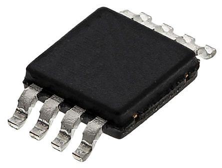
| 描述 | IC DAC 12BIT SERIAL IN 8MSOP数模转换器- DAC 12-Bit Serial Input Multiplying |
| 产品分类 | |
| 品牌 | Analog Devices Inc |
| 产品手册 | |
| 产品图片 |
|
| rohs | 符合RoHS无铅 / 符合限制有害物质指令(RoHS)规范要求 |
| 产品系列 | 数据转换器IC,数模转换器- DAC,Analog Devices AD5441BRMZ- |
| 数据手册 | |
| 产品型号 | AD5441BRMZ |
| 产品培训模块 | http://www.digikey.cn/PTM/IndividualPTM.page?site=cn&lang=zhs&ptm=19145http://www.digikey.cn/PTM/IndividualPTM.page?site=cn&lang=zhs&ptm=18614http://www.digikey.cn/PTM/IndividualPTM.page?site=cn&lang=zhs&ptm=26125http://www.digikey.cn/PTM/IndividualPTM.page?site=cn&lang=zhs&ptm=26140http://www.digikey.cn/PTM/IndividualPTM.page?site=cn&lang=zhs&ptm=26150http://www.digikey.cn/PTM/IndividualPTM.page?site=cn&lang=zhs&ptm=26147 |
| 产品目录页面 | |
| 产品种类 | 数模转换器- DAC |
| 位数 | 12 |
| 供应商器件封装 | 8-MSOP |
| 分辨率 | 12 bit |
| 包装 | 管件 |
| 商标 | Analog Devices |
| 安装类型 | 表面贴装 |
| 安装风格 | SMD/SMT |
| 封装 | Tube |
| 封装/外壳 | 8-TSSOP,8-MSOP(0.118",3.00mm 宽) |
| 封装/箱体 | MSOP-8 |
| 工作温度 | -40°C ~ 125°C |
| 工厂包装数量 | 50 |
| 建立时间 | 500ns |
| 接口类型 | Serial |
| 数据接口 | 串行 |
| 最大功率耗散 | 55 uW |
| 最大工作温度 | + 125 C |
| 最小工作温度 | - 40 C |
| 标准包装 | 50 |
| 电压参考 | External |
| 电压源 | 单电源 |
| 电源电压-最大 | 5.5 V |
| 电源电压-最小 | 2.5 V |
| 积分非线性 | +/- 0.5 LSB |
| 稳定时间 | 500 ns |
| 系列 | AD5441 |
| 结构 | R-2R |
| 转换器数 | 1 |
| 转换器数量 | 1 |
| 输出数和类型 | 1 电流 |
| 输出类型 | Current |
| 配用 | /product-detail/zh/EVAL-AD5541%2F42EBZ/EVAL-AD5541%2F42EBZ-ND/1825562 |
| 采样比 | 5 MSPs |
| 采样率(每秒) | - |


- 商务部:美国ITC正式对集成电路等产品启动337调查
- 曝三星4nm工艺存在良率问题 高通将骁龙8 Gen1或转产台积电
- 太阳诱电将投资9.5亿元在常州建新厂生产MLCC 预计2023年完工
- 英特尔发布欧洲新工厂建设计划 深化IDM 2.0 战略
- 台积电先进制程称霸业界 有大客户加持明年业绩稳了
- 达到5530亿美元!SIA预计今年全球半导体销售额将创下新高
- 英特尔拟将自动驾驶子公司Mobileye上市 估值或超500亿美元
- 三星加码芯片和SET,合并消费电子和移动部门,撤换高东真等 CEO
- 三星电子宣布重大人事变动 还合并消费电子和移动部门
- 海关总署:前11个月进口集成电路产品价值2.52万亿元 增长14.8%


PDF Datasheet 数据手册内容提取
12-Bit Serial Input Multiplying DAC AD5441 FEATURES FUNCTIONAL BLOCK DIAGRAM 2.5 V to 5.5 V supply operation AD5441 True 12-bit accuracy VDD RFB 5 V operation @ <1 μA VREF DAC IOUT Fast 3-wire serial input 12 Fast 5 μs settling time 1.9 MHz, 4-quadrant multiply BW LD DAC REG Upgrade for DAC8043 and DAC8043A 12 Standard and rotated pinout GND CLK 12-BIT SHIFT APPLICATIONS SRI REGISTER 06492-001 Figure 1. Ideal for PLC applications in industrial control Programmable amplifiers and attenuators Digitally controlled calibration and filters Motion control systems GENERAL DESCRIPTION The AD5441 is an improved high accuracy 12-bit multiplying digital-to-analog converter (DAC) in space-saving 8-lead packages. Featuring serial input, double buffering, and excellent analog performance, the AD5441 is ideal for applications where PC board space is at a premium. Improved linearity and gain error performance permit reduced part counts through the elimination of trimming components. Separate input clock and load DAC control lines allow full user control of data loading and analog output. The circuit consists of a 12-bit serial-in/parallel-out shift register, a 12-bit DAC register, a 12-bit CMOS DAC, and control logic. Serial data is clocked into the input register on the rising edge of the clock pulse. When the new data-word is clocked in, it is loaded into the DAC register with the LD input pin. Data in the DAC register is converted to an output current by the DAC. Consuming only 1 μA from a single 5 V power supply, the AD5441 is the ideal low power, small size, high performance solution to many application problems. The AD5441 is specified over the extended industrial (−40°C to +125°C) temperature range. It is available in an 8-lead LFCSP and an 8-lead MSOP. Rev. A Information furnished by Analog Devices is believed to be accurate and reliable. However, no responsibility is assumed by Analog Devices for its use, nor for any infringements of patents or other One Technology Way, P.O. Box 9106, Norwood, MA 02062-9106, U.S.A. rights of third parties that may result from its use. Specifications subject to change without notice. No license is granted by implication or otherwise under any patent or patent rights of Analog Devices. Tel: 781.329.4700 www.analog.com Trademarks and registered trademarks are the property of their respective owners. Fax: 781.461.3113 ©2008–2011 Analog Devices, Inc. All rights reserved.
AD5441 TABLE OF CONTENTS Features..............................................................................................1 Typical Performance Characteristics..............................................7 Applications.......................................................................................1 Terminology....................................................................................10 Functional Block Diagram..............................................................1 Parameter Definitions....................................................................11 General Description.........................................................................1 General Circuit Information.....................................................11 Revision History...............................................................................2 Output Impedance.....................................................................11 Specifications.....................................................................................3 Applications Information..........................................................11 Electrical Characteristics.............................................................3 Unipolar 2-Quadrant Multiplying...........................................11 Timing Characteristics................................................................4 Bipolar 4-Quadrant Multiplying..............................................12 Absolute Maximum Ratings............................................................5 Interface Logic Information......................................................12 Thermal Resistance......................................................................5 Digital Section............................................................................12 ESD Caution..................................................................................5 Outline Dimensions.......................................................................13 Pin Configurations and Function Descriptions...........................6 Ordering Guide..........................................................................13 REVISION HISTORY 3/11—Rev. 0 to Rev. A Deleted Figure 2................................................................................4 Added Timing Diagrams Section...................................................4 Added New Figure 2, Figure 3, and Figure 4, Renumbered Figures Sequentially.........................................................................4 Changes to Figure 5 and Table 6.....................................................6 Updated Outline Dimensions.......................................................13 Changes to Ordering Guide..........................................................13 1/08—Revision 0: Initial Version Rev. A | Page 2 of 16
AD5441 SPECIFICATIONS ELECTRICAL CHARACTERISTICS V = 5 V, V = 10 V, −40°C < T < +155°C, unless otherwise noted. DD REF A Table 1. Parameter Symbol Min Typ Max Unit Condition STATIC PERFORMANCE Resolution N 12 Bits Relative Accuracy INL ±0.5 LSB Differential Nonlinearity DNL ±0.5 LSB All grades monotonic to 12 bits Gain Error G ±1 LSB Data = FFF FSE H Gain Temperature Coefficient1 TCG ±5 ppm/°C I pin measured FS OUT Output Leakage Current I ±5 nA Data = 000 , I pin measured LKG H OUT ±25 nA T = –40°C, +125°C, data = 000 , I pin measured A H OUT Zero-Scale Error I ±0.03 LSB Data = 000 ZSE H ±0.15 LSB T = −40°C, +125°C, data = 000 A H REFERENCE INPUT Input Resistance R 7 15 kΩ Absolute temperature coefficient < 50 ppm/°C REF Input Capacitance1 C 5 pF REF ANALOG OUTPUT Output Capacitance1 C 1 pF Data = 000 OUT H 4 pF Data = FFF H DIGITAL INPUTS Digital Input Low V 0.8 V IL Digital Input High V 2.4 V IH Input Leakage Current I 1 μA V = 0 V to 5 V IL LOGIC Input Capacitance1 C 4.0 pF V = 0 V IL LOGIC AC CHARACTERISTICS1 Output Current Settling Time t 5 μs To ±0.01% of full-scale, external op amp OP42 S 0.5 μs To ±0.01% of full-scale, 100 Ω terminated to ground DAC Glitch Q 40 nVs Data = 000 to FFF to 000 , V = 0 V, OP42 H H H REF 1 nVs Data = 000 to FFF to 000 , V = 0 V, 100 Ω H H H REF Digital Feedthrough 5 nV Using external op amp OP42 Feedthrough (V /V ) FT 1.4 mV p-p V = 20 V p-p, data = 000 , f = 10 kHz OUT REF REF H Total Harmonic Distortion THD −85 dB V = 6 V rms, data = FFF , f = 1 kHz REF H Output Noise Density e 17 nV/√Hz 10 Hz to 100 kHz between R and I n FB OUT Multiplying Bandwidth BW 1.9 MHz −3 dB, V /V , V = 100 mV rms, data = FFF OUT REF REF H SUPPLY CHARACTERISTICS1 Power Supply Range V 2.5 5.5 V DD RANGE Positive Supply Current I 10 μA V = 0 V or V DD LOGIC DD Power Dissipation P 2.5 5.5 μW V = 0 V or V DISS LOGIC DD Power Supply Sensitivity PSS 0.002 %/% ΔV = ±5% DD 1 These parameters are guaranteed by design and not subject to production testing. Rev. A | Page 3 of 16
AD5441 TIMING CHARACTERISTICS All input control signals are specified with t = t = 2 ns (10% to 90% of V ) and timed from a voltage level of (V + V )/2; V + 2.5 V R F DD IL IH DD to 5.5 V, V = 10 V; temperature range = −40°C to +125°C; all specifications T to T , unless otherwise noted. REF MIN MAX Table 2. Timing Characteristics Parameter 2.5 V 5.5 V Unit Conditions/Comments t 10 5 ns min Data setup DS t 5 5 ns min Data hold DH t 15 10 ns min Clock width high CH t 15 10 ns min Clock width low CL t 20 10 ns min Load pulse width LD t 0 0 ns min LD DAC high to MSB CLK high LD1 t 0 0 ns min LSB CLK to LD DAC ASB Timing Diagrams SRI D11 D10 D9 D8 D7 D6 D5 D4 D3 D2 D1 D0 CLK tLD1 tASB LD DAC REGISTER LOAD 06492-102 Figure 2. Full Data Transmission DATA LOADED MSB(D11) FIRST SRI Dxx t t DS DH CLK tCL tCH 06492-103 Figure 3. Bit Data Transmission t LD LD FS ±1LSB VOUTZS ERROR BAND 06492-104 Figure 4. Output Transition Table 3. Control Logic Truth Table CLK LD Serial Shift Register Function DAC Register Function ↑1 H Shift register data advanced one bit Latched ↑ L Shift register data advanced one bit Transparent H or L L No effect Updated with current shift register contents L ↑1 No effect Latched all 12 bits 1 ↑ equals positive logic transition. Rev. A | Page 4 of 16
AD5441 ABSOLUTE MAXIMUM RATINGS Table 4. THERMAL RESISTANCE Parameter Rating VDD to GND −0.3 V, +8 V θJA is specified for the worst-case conditions, that is, a device V to GND ±18 V soldered in a circuit board for surface-mount packages. REF R to GND ±18 V FB Table 5. Logic Inputs to GND −0.3 V, V + 0.3 V DD Package Type θ θ Unit I to GND −0.3 V, V + 0.3 V JA JC OUT DD 8-Lead MSOP 142 44 °C/W I Short Circuit to GND 50 mA OUT 8-Lead LFCSP1 75 18 °C/W Package Power Dissipation (T max − T )/θ J A JA Maximum Junction Temperature (TJ max) 150°C 1 Exposed pad soldered to the ground plane. Operating Temperature Range −40°C to +125°C Storage Temperature Range −65°C to +150°C ESD CAUTION Lead Temperature (Soldering, 10 sec) 300°C Stresses above those listed under Absolute Maximum Ratings may cause permanent damage to the device. This is a stress rating only; functional operation of the device at these or any other conditions above those indicated in the operational section of this specification is not implied. Exposure to absolute maximum rating conditions for extended periods may affect device reliability. Rev. A | Page 5 of 16
AD5441 PIN CONFIGURATIONS AND FUNCTION DESCRIPTIONS PIN 1 VREF 1 8 VDD VREF1 INDICATOR 8 VDD RFB 2 AD5441 7 CLK GIRONFUDBT234 (NTAoOtD Pto5 V 4SIE4caW1le) 765 SLCDRLKI GIONUDT 34 (NToOt Pto V SIEcaWle) 65 SLDRI 06492-004 N1.O CTTHOEENS NEEXCPTOESDE DT OP ATDH ES HGORUOLUDN DB EPLANE. 06492-003 Figure 5. 8-Lead LFCSP Pin Configuration Figure 6. 8-Lead MSOP Pin Configuration Table 6. Pin Function Descriptions Pin No. Mnemonic Description 1 V DAC Reference Input Pin. Establishes DAC full-scale voltage. Constant input resistance vs. code. REF 2 R Internal Matching Feedback Resistor. Connect to external op amp output. FB 3 I DAC Current Output, full-scale output 1 LSB less than reference input voltage −V . OUT REF 4 GND Analog and Digital Ground. 5 LD Load Strobe, Level-Sensitive Digital Input. Transfers shift-register data to DAC register while active low. See Table 3 for operation. 6 SRI 12-Bit Serial Register Input. Data loads directly into the shift register MSB first. Extra leading bits are ignored. 7 CLK Clock Input. Positive-edge clocks data into shift register. 8 V Positive Power Supply Input. Specified range of operation 5 V ± 10%. DD EP Exposed Pad. The exposed pad should be connected to the ground plane. Rev. A | Page 6 of 16
AD5441 TYPICAL PERFORMANCE CHARACTERISTICS 0.5 0.5 TA=25°C TA=25°C 0.4 VREF=10V 0.4 VREF=10V VDD=3V VDD= 5V 0.3 0.3 0.2 0.2 B) 0.1 B) 0.1 S S L (L 0 L (L 0 N N I –0.1 I –0.1 –0.2 –0.2 –0.3 –0.3 ––00..45 06492-039 ––00..45 06492-040 0 500 1000 1500 2000 2500 3000 3500 4000 0 500 1000 1500 2000 2500 3000 3500 4000 CODE CODE Figure 7. INL vs. Code, 3 V Figure 10. INL vs. Code, 5 V 0.5 0.5 TA=25°C TA=25°C 0.4 VREF=10V 0.4 VREF=10V VDD=3V VDD= 5V 0.3 0.3 0.2 0.2 B) 0.1 B) 0.1 S S L (L 0 L (L 0 N N D –0.1 D –0.1 –0.2 –0.2 –0.3 –0.3 ––00..45 06492-037 ––00..45 06492-038 0 500 1000 1500 2000 2500 3000 3500 4000 0 500 1000 1500 2000 2500 3000 3500 4000 CODE CODE Figure 8. DNL vs. Code, 3 V Figure 11. DNL vs. Code, 5 V 0.25 100 MAXINL 0.20 0.15 75 0.10 Y NL (LSB) 0.050 EQUENC 50 I R F –0.05 25 –0.10 MININL ––00..1250 TVADD==2 55°VC 06492-042 0 0 1 2 3REFE4RENC5E VOL6TAGE7 8 9 10 –1.0 T–O0.T5AL UNADJU0STED ERROR0 (.L5SB) 1.0 06492-048 Figure 9. INL vs. Reference, 5 V Figure 12. Total Unadjusted Error Histogram Rev. A | Page 7 of 16
AD5441 4 0.050 TA = 25°C TA = 25°C VREF = 10V 0.045 VDD = 5V OP42 0.040 2 0.035 L (LSB) 0 RENT (µA) 00..003205 N R I CU 0.020 VDD = 3V 0.015 –2 VDD = 5V 0.010 –4 0.0050 06492-044 –2000 –1000OP AMP OFF0SET, VOS (µV)1000 2000 06492-049 –60 –40 –20 0TEM2P0ERAT4U0RE (°6C0) 80 100 120 Figure 13. Integral Nonlinearity Error vs. External Op Amp Figure 16. Supply Current vs. Temperature 1400 50 1200 40 1000 RENT (µA) 800 F55 QUENCY 30 R 600 E U R 20 C F 400 10 200 800 0 FFF 06492-035 0 10k 100k FREQU1EMNCY (Hz) 10M 100M 0 FULL-SCALE 1TEMPERATURE C2OEFFICIENT (pp3m/°C) 06492-046 Figure 14. Supply Current vs. Clock Frequency Figure 17. Full-Scale Output Temperature Coefficient Histogram 0.20 5.34 6 TA = 25°C LDAC 5 0.18 5.32 4 0.16 5.30 3 CURRENT (µA) 0000....11104208 TPUT VOLTAGE (V) 55555.....2222286420 TV7RVFARDISF ED=IFNT =2=OG 55 1° V8EC00DV0GE 210––––1234 V (V)LOAD 0.06 OU 5.18 –5 –6 0.04 5.16 –7 0.0200 0.5 1.0 1.5INP2U.0T VO2.L5TAG3E.0 (V)3.5 4.0 4.5 5.006492-043 55..1142–0.2 0 0.2 0.4 TIM0.E6 (µs)0.8 1.0 1.2 1.4 –––8910 06492-033 Figure 15. Supply Current vs. Logic Input Voltage Figure 18. Midscale Transitions Rev. A | Page 8 of 16
AD5441 4 100 ALL BIOTNS TVAR E=F 2=5 °1C0V –8 VDD = 5V 80 –20 B) d N ( –32 B) 60 O d ENUATI –44 PSRR ( 40 T T A –56 20 ––8608 TVVARD ED=F = 2= 55 °1VC00mV rms 0 06492-027 100 1k F1R0EkQUENCY 1(0H0zk) 1M 10M06492-045 1k 10k FREQU1E00NkCY (Hz) 1M 10M Figure 19. Reference Multiplying Bandwidth Figure 20. PSRR vs. Frequency Rev. A | Page 9 of 16
AD5441 TERMINOLOGY Digital Feedthrough Relative Accuracy (INL) When the device is not selected, high frequency logic activity Relative accuracy or endpoint nonlinearity is a measure of the on the digital inputs of the device may be capacitively coupled maximum deviation from a straight line passing through the through the device and produce noise on the I pins. This endpoints of the DAC transfer function. It is measured after OUT noise is coupled from the outputs of the device onto follow-on adjusting for zero and full scale and is normally expressed in circuitry. This noise is digital feedthrough. LSBs or as a percentage of the full-scale reading. Multiplying Feedthrough Error Differential Nonlinearity (DNL) This is the error due to capacitive feedthrough from the DAC DNL is the difference between the measured change and the reference input to the DAC I 1 terminal when all 0s are ideal 1 LSB change between any two adjacent codes. A specified OUT loaded to the DAC. differential nonlinearity of −1 LSB maximum over the operating temperature range ensures monotonicity. Total Harmonic Distortion (THD) The DAC is driven by an ac reference. The ratio of the rms sum Gain Error of the harmonics of the DAC output to the fundamental value is Gain error or full-scale error is a measure of the output error the THD. Usually only the lower order harmonics, such as between an ideal DAC and the actual device output. For these second to fifth, are included. DACs, ideal maximum output is V − 1 LSB. Gain error of the REF DACs is adjustable to zero with external resistance. V22+V32+V42+V52 THD=20log Zero Scale Error V1 Calculated from worst-case R REF Compliance Voltage Range IZSE(LSB) = (RREF × ILKG × 4096)/VREF. The maximum range of (output) terminal voltage for which the device provides the specified characteristics. Output Leakage Current Output leakage current is the current that flows into the DAC Output Noise Spectral Density ladder switches when they are turned off. For the I terminal, OUT Calculation from it can be measured by loading all 0s to the DAC and measuring e = √4KTRB the I current. n OUT where: Output Capacitance K is Boltzmann Constant (J/°K). Capacitance from I 1 to AGND. OUT R is resistance (Ω). Digital-to-Analog Glitch Impulse T is the resistor temperature (°K). The amount of charge injected from the digital inputs to the B is the 1 Hz bandwidth. analog output when the inputs change state. This is normally specified as the area of the glitch in either pA-s or nV-s, depending on whether the glitch is measured as a current or voltage signal. Rev. A | Page 10 of 16
AD5441 PARAMETER DEFINITIONS GENERAL CIRCUIT INFORMATION During any testing of the resistor ladder or RFEEDBACK (such as incoming inspection), V must be present to turn on these DD The AD5441 is a 12-bit multiplying DAC with a low series switches. temperature coefficient. It contains an R-2R resistor ladder OUTPUT IMPEDANCE network, data input and control logic, and two data registers. The output resistance of the AD5441, as in the case of the The digital circuitry forms an interface in which serial data can output capacitance, varies with the digital input code. This be loaded under microprocessor control into a 12-bit shift register and then transferred, in parallel, to the 12-bit DAC register. resistance, looking back into the IOUT terminal, may be between 10 kΩ (the feedback resistor alone when all digital inputs are The analog portion of the AD5441 contains an inverted R-2R low) and 7.5 kΩ (the feedback resistor in parallel with approximate ladder network consisting of silicon-chrome, highly stable 30 kΩ of the R-2R ladder network resistance when any single bit (50 ppm/°C), thin-film resistors, and 12 pairs of NMOS current- logic is high). Static accuracy and dynamic performance are steering switches, see Figure 21. These switches steer binarily affected by these variations. weighted currents into either I or GND; this yields a constant OUT APPLICATIONS INFORMATION current in each ladder leg, regardless of digital input code. This constant current results in a constant input resistance at VREF In most applications, linearity depends upon the potential of equal to R. The VREF input may be driven by any reference voltage the IOUT and GND pins being at the same voltage potential. The or current, ac or dc, that is within the limits stated in the DAC is connected to an external precision op amp inverting input. Absolute Maximum Ratings. The external amplifiers noninverting input should be tied directly 10kΩ 10kΩ 10kΩ to ground without the usual bias current compensating resistor (see VREF Figure 22 and Figure 24). The selected amplifier should have a low 20kΩ 20kΩ 20kΩ 20kΩ 20kΩ input bias current and low drift over temperature. The amplifiers S1 S2 S3 S12 * input offset voltage should be nulled to less than 200 mV (less than 10% of 1 LSB). All grounded pins should tie to a single common GND ground point to avoid ground loops. The V power supply should IOUT DD 10kΩ have a low noise level with adequate bypassing. It is best to operate * RFEEDBACK the AD5441 from the analog power supply and grounds. BIT 1 (MSB) BIT2 BIT3 BIT 12 (LSB) DIGITAL INPUTS UNIPOLAR 2-QUADRANT MULTIPLYING *THESE SWITCHES PERMANENTLY ON. The most straightforward application of the AD5441 is in the N1.O STWEISTCHES SHOWN FOR DIGITAL INPUTS HIGH. 06492-021 2-quadrant multiplying configuration shown in Figure 22. If the Figure 21. Simplified DAC Circuit reference input signal is replaced with a fixed dc voltage reference, the DAC output provides a proportional dc voltage output The 12 output current steering NMOS FET switches are in according to the transfer equation series with each R-2R resistor. V = −D/4096 × V OUT REF To further ensure accuracy across the full temperature range, MOS switches that are always on were included in series with where: the feedback resistor and the terminating resistor of the R-2R D is the decimal data loaded into the DAC register. ladder. Figure 21 shows the location of the series switches. VREF is the externally applied reference voltage source. VDD R2 VDD RFB C1 IOUT1 VREF VREF AD5441 A1 R1 GND VOUT = 0 TO –VREF LD CLK SRI AGND µCONTROLLER NOTES 21..ICRF11 A PA1HN IADSS RAE2 H CUIOGSMHE DPS EPONENSELADYT AIIFOM NGP AL(1IIpFNFI EA TRDO.J U2SpTFM) MENATY IBSE R REEQQUUIRIREEDD. 06492-023 Figure 22. Unipolar (2-Quadrant) Operation Rev. A | Page 11 of 16
AD5441 BIPOLAR 4-QUADRANT MULTIPLYING DIGITAL SECTION Figure 24 shows a suggested circuit to achieve 4-quadrant The digital inputs of the AD5441, SRI, LD, and CLK, are TTL- multiplying operation. The summing amplifier multiplies VOUT1 compatible. The input voltage levels affect the amount of current by 2 and offsets the output with the reference voltage so that a drawn from the supply; peak supply current occurs as the digital midscale digital input code of 2048 places VOUT2 at 0 V. The negative input (VIN) passes through the transition region. See Figure 15 full-scale voltage is VREF when the DAC is loaded with all zeros. for the supply current vs. logic input voltage graph. Maintaining The positive full-scale output is −(VREF − 1 LSB) when the DAC the digital input voltage levels as close as possible to the supplies, is loaded with all ones. Therefore, the digital coding is offset V and GND, minimizes supply current consumption. The DD binary. The voltage output transfer equation for various input digital inputs of the AD5441 were designed with ESD resistance data and reference (or signal) values follows incorporated through careful layout and the inclusion of input protection circuitry. Figure 23 shows the input protection diodes V = (D/2048 − 1) − V OUT2 REF and series resistor; this input structure is duplicated on each where: digital input. High voltage static charges applied to the inputs D is the decimal data loaded into the DAC register. are shunted to the supply and ground rails through forward- V is the externally applied reference voltage source. REF biased diodes. These protection diodes were designed to clamp INTERFACE LOGIC INFORMATION the inputs to well below dangerous levels during static discharge conditions. The AD5441 has been designed for ease of operation. The timing diagram in Figure 2 illustrates the input register loading VDD sequence. Note that the most significant bit (MSB) is loaded first. Once the 12-bit input register is full, the data is transferred 5kΩ LD, CLK, SRI to the DAC register by taking LD momentarily low. GND 06492-020 Figure 23. Digital Input Protection R3 20kΩ VDD R2 R5 20kΩ VDD RFB C1 R4 V±1R0EVF VREF AD5441 IOUT1 A1 10kΩ R1 GND A2 VOUT = –VREF TO +VREF LD CLK SRI AGND µCONTROLLER NOTES 1.R1 AND R2 ARE USED ONLY IF GAIN ADJUSTMENT IS REQUIRED. ADJUST R1 FOR VOUT = 0V WITH CODE 10000000 LOADED TO DAC. 2.MATCHING AND TRACKING IS ESSENTIAL FOR RESISTOR PAIRS 3.RICF31 A PA1HN/AAD2S R EIS4 .C AO HMIGPEHN SSPAETEIODN A (M1PpFL ITFOIE R2p.F) MAY BE REQUIRED 06492-024 Figure 24. Bipolar (4-Quadrant) Operation Rev. A | Page 12 of 16
AD5441 OUTLINE DIMENSIONS 0.35 3.00 0.30 0.65 BSC BSC SQ 0.25 5 8 PIN 1 IANRDEEAX *EXPPAODSED 11..7644 (BOTTOM VIEW) 0.50 1.49 0.40 0.30 4 1 PIN 1 INDICATOR TOP VIEW 2.48 (R 0.2) 2.38 0.80 MAX 0.80 0.55 NOM 2.23 0.75 0.05 MAX 0.70 0.02 NOM SEATING PLANE 0.20 REF *FOTOHFER T PHPIIRNSO CDPOAETNRAF C ISGOHUNERNEAETTC.ITOINO NA NODF FTUHNEC ETXIOPON SDEEDS CPRAIDP TPILOENASS SEE RCETFIOERN TO 022808-B Figure 25. 8-Lead Lead Frame Chip Scale Package [LFCSP_WD] 3 mm × 3 mm Body, Very Very Thin, Dual Lead (CP-8-3) Dimensions are shown in millimeters 3.20 3.00 2.80 8 5 5.15 3.20 4.90 3.00 4.65 2.80 1 4 PIN 1 0.65 BSC 0.95 0.85 1.10 MAX 0.75 0.80 0.15 0.38 0.23 8° 0.60 0.00 0.22 0.08 0° 0.40 COPLANARITY SEATING 0.10 PLANE COMPLIANT TO JEDEC STANDARDS MO-187-AA Figure 26. 8-Lead Mini Small Outline Package [MSOP] (RM-8) Dimensions are shown in millimeters ORDERING GUIDE Model1 INL (LSB) Temperature Range Package Description Package Option Branding AD5441BCPZ-R2 ±0.5 −40°C to +125°C 8-Lead LFCSP_WD CP-8-3 DBD AD5441BCPZ-REEL7 ±0.5 −40°C to +125°C 8-Lead LFCSP_WD CP-8-3 DBD AD5441BRMZ ±0.5 −40°C to +125°C 8-Lead MSOP RM-8 DBC AD5441BRMZ-REEL7 ±0.5 −40°C to +125°C 8-Lead MSOP RM-8 DBC 1 Z = RoHS Compliant Part. Rev. A | Page 13 of 16
AD5441 NOTES Rev. A | Page 14 of 16
AD5441 NOTES Rev. A | Page 15 of 16
AD5441 NOTES ©2008–2011 Analog Devices, Inc. All rights reserved. Trademarks and registered trademarks are the property of their respective owners. D06492-0-3/11(A) Rev. A | Page 16 of 16
Mouser Electronics Authorized Distributor Click to View Pricing, Inventory, Delivery & Lifecycle Information: A nalog Devices Inc.: AD5441BCPZ-REEL7 AD5441BRMZ-REEL7 AD5441BRMZ