ICGOO在线商城 > 集成电路(IC) > 数据采集 - 数模转换器 > AD5424YRUZ
 Datasheet下载
- 型号: AD5424YRUZ
- 制造商: Analog
- 库位|库存: xxxx|xxxx
- 要求:
| 数量阶梯 | 香港交货 | 国内含税 |
| +xxxx | $xxxx | ¥xxxx |
查看当月历史价格
查看今年历史价格
AD5424YRUZ产品简介:
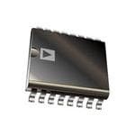
ICGOO电子元器件商城为您提供AD5424YRUZ由Analog设计生产,在icgoo商城现货销售,并且可以通过原厂、代理商等渠道进行代购。 AD5424YRUZ价格参考。AnalogAD5424YRUZ封装/规格:数据采集 - 数模转换器, 8 位 数模转换器 1 16-TSSOP。您可以下载AD5424YRUZ参考资料、Datasheet数据手册功能说明书,资料中有AD5424YRUZ 详细功能的应用电路图电压和使用方法及教程。
AD5424YRUZ 是由 Analog Devices Inc.(ADI)生产的一款数据采集 - 数模转换器(DAC)。其主要应用场景包括以下方面:

1. 工业自动化与控制:
   AD5424YRUZ 可用于工业自动化系统中,将数字信号转换为模拟信号,以驱动执行器、阀门或电机控制器。它支持高精度的电压输出,适用于需要精确控制的应用,如过程控制、温度调节和压力控制。

2. 仪器仪表:
   在精密测量仪器中,AD5424YRUZ 能够提供稳定的模拟输出信号,用于校准设备或生成测试波形。例如,在示波器、信号发生器或数据记录仪中,该 DAC 可确保高分辨率和低噪声性能。

3. 通信系统:
   该器件可用于通信设备中的信号调制与解调,例如生成射频信号的基带部分或实现数字预失真功能。其快速转换能力和低失真特性使其适合高速通信应用。

4. 医疗设备:
   在医疗领域,AD5424YRUZ 可用于医疗成像设备(如超声波或核磁共振)、患者监护仪或诊断设备中,提供精确的模拟信号输出以驱动传感器或显示单元。

5. 消费电子:
   它可以应用于音频设备中,将数字音频信号转换为模拟信号,从而驱动扬声器或耳机。此外,在家用自动化系统中,也可以用作信号生成器或控制器的一部分。

6. 汽车电子:
   在汽车行业中,AD5424YRUZ 可用于车载信息娱乐系统、驾驶辅助系统或电动车辆的动力管理系统中,提供可靠的模拟输出以支持实时控制需求。

总结来说,AD5424YRUZ 凭借其高性能和可靠性,广泛适用于需要高精度数模转换的场景,涵盖工业、通信、医疗、消费电子及汽车等多个领域。
| 参数 | 数值 |
| 产品目录 | 集成电路 (IC)半导体 |
| 描述 | IC DAC 8BIT MULTIPLYING 16-TSSOP数模转换器- DAC 8-BIT PARELLED INTERFACE IC |
| 产品分类 | |
| 品牌 | Analog Devices Inc |
| 产品手册 | |
| 产品图片 |
|
| rohs | 符合RoHS无铅 / 符合限制有害物质指令(RoHS)规范要求 |
| 产品系列 | 数据转换器IC,数模转换器- DAC,Analog Devices AD5424YRUZ- |
| 数据手册 | |
| 产品型号 | AD5424YRUZ |
| 产品培训模块 | http://www.digikey.cn/PTM/IndividualPTM.page?site=cn&lang=zhs&ptm=19145http://www.digikey.cn/PTM/IndividualPTM.page?site=cn&lang=zhs&ptm=18614http://www.digikey.cn/PTM/IndividualPTM.page?site=cn&lang=zhs&ptm=26125http://www.digikey.cn/PTM/IndividualPTM.page?site=cn&lang=zhs&ptm=26140http://www.digikey.cn/PTM/IndividualPTM.page?site=cn&lang=zhs&ptm=26150http://www.digikey.cn/PTM/IndividualPTM.page?site=cn&lang=zhs&ptm=26147 |
| 产品目录页面 | |
| 产品种类 | 数模转换器- DAC |
| 位数 | 8 |
| 供应商器件封装 | 16-TSSOP |
| 分辨率 | 8 bit |
| 包装 | 管件 |
| 商标 | Analog Devices |
| 安装类型 | 表面贴装 |
| 安装风格 | SMD/SMT |
| 封装 | Tube |
| 封装/外壳 | 16-TSSOP(0.173",4.40mm 宽) |
| 封装/箱体 | TSSOP-16 |
| 工作温度 | -40°C ~ 125°C |
| 工厂包装数量 | 96 |
| 建立时间 | 80ns |
| 接口类型 | Parallel |
| 数据接口 | 并联 |
| 最大功率耗散 | 25 uW |
| 最大工作温度 | + 125 C |
| 最小工作温度 | - 40 C |
| 标准包装 | 96 |
| 电压参考 | External |
| 电压源 | 单电源 |
| 电源电压-最大 | 5.5 V |
| 电源电压-最小 | 2.5 V |
| 积分非线性 | +/- 0.25 LSB |
| 稳定时间 | 30 ns |
| 系列 | AD5424 |
| 结构 | R-2R |
| 转换器数 | 1 |
| 转换器数量 | 1 |
| 输出数和类型 | 2 电流 |
| 输出类型 | Current |
| 配用 | /product-detail/zh/EVAL-AD5424EBZ/EVAL-AD5424EBZ-ND/1679960 |
| 采样比 | 20.4 MSPs |
| 采样率(每秒) | 20.4M |


- 商务部:美国ITC正式对集成电路等产品启动337调查
- 曝三星4nm工艺存在良率问题 高通将骁龙8 Gen1或转产台积电
- 太阳诱电将投资9.5亿元在常州建新厂生产MLCC 预计2023年完工
- 英特尔发布欧洲新工厂建设计划 深化IDM 2.0 战略
- 台积电先进制程称霸业界 有大客户加持明年业绩稳了
- 达到5530亿美元!SIA预计今年全球半导体销售额将创下新高
- 英特尔拟将自动驾驶子公司Mobileye上市 估值或超500亿美元
- 三星加码芯片和SET,合并消费电子和移动部门,撤换高东真等 CEO
- 三星电子宣布重大人事变动 还合并消费电子和移动部门
- 海关总署:前11个月进口集成电路产品价值2.52万亿元 增长14.8%


PDF Datasheet 数据手册内容提取
8-/10-/12-Bit, High Bandwidth Multiplying DACs with Parallel Interface Data Sheet AD5424/AD5433/AD5445 FEATURES GENERAL DESCRIPTION 2.5 V to 5.5 V supply operation The AD5424/AD5433/AD54451 are CMOS 8-, 10-, and 12-bit Fast parallel interface (17 ns write cycle) current output digital-to-analog converters (DACs), respectively. Update rate of 20.4 MSPS These devices operate from a 2.5 V to 5.5 V power supply, INL of ±1 LSB for 12-bit DAC making them suitable for battery-powered applications and 10 MHz multiplying bandwidth many other applications. These DACs utilize data readback, ±10 V reference input allowing the user to read the contents of the DAC register via Extended temperature range: –40°C to +125°C the DB pins. On power-up, the internal register and latches are 20-lead TSSOP and chip scale (4 mm × 4 mm) packages filled with 0s and the DAC outputs are at zero scale. 8-, 10-, and 12-bit current output DACs As a result of manufacturing with a CMOS submicron process, Upgrades to AD7524/AD7533/AD7545 they offer excellent 4-quadrant multiplication characteristics, Pin-compatible 8-, 10-, and 12-bit DACs in chip scale with large signal multiplying bandwidths of up to 10 MHz. Guaranteed monotonic 4-quadrant multiplication The applied external reference input voltage (VREF) determines the Power-on reset with brownout detection full-scale output current. An integrated feedback resistor (RFB) Readback function provides temperature tracking and full-scale voltage output 0.4 µA typical power consumption when combined with an external I-to-V precision amplifier. APPLICATIONS While these devices are upgrades of the AD5424/AD5433/ AD5445 in multiplying bandwidth performance, they have a Portable battery-powered applications latched interface and cannot be used in transparent mode. Waveform generators Analog processing The AD5424 is available in a small, 20-lead LFCSP and a small, Instrumentation applications 16-lead TSSOP, while the AD5433 and AD5445 DACs are available Programmable amplifiers and attenuators in a small, 20-lead LFCSP and a small, 20-lead TSSOP. Digitally controlled calibration The EVAL-AD5445SDZ evaluation board is available for Programmable filters and oscillators evaluating DAC performance. For more information, see the Composite video UG-333 evaluation board user guide. Ultrasound Gain, offset, and voltage trimming 1 U.S Patent No. 5,689,257. FUNCTIONAL BLOCK DIAGRAM VDD VREF AD5424/ R RFB AD5433/ 8-/10-/12-BIT IOUT1 AD5445 R-2R DAC IOUT2 POWER-ON DAC REGISTER RESET CS INPUT LATCH R/W GND DB0INDPAUTTASDB7/DB9/DB11 03160-001 Figure 1. Rev. E Document Feedback Information furnished by Analog Devices is believed to be accurate and reliable. However, no responsibility is assumed by Analog Devices for its use, nor for any infringements of patents or other One Technology Way, P.O. Box 9106, Norwood, MA 02062-9106, U.S.A. rights of third parties that may result from its use. Specifications subject to change without notice. No license is granted by implication or otherwise under any patent or patent rights of Analog Devices. Tel: 781.329.4700 ©2003–2016 Analog Devices, Inc. All rights reserved. Trademarks and registered trademarks are the property of their respective owners. Technical Support www.analog.com
AD5424/AD5433/AD5445 Data Sheet TABLE OF CONTENTS Features .............................................................................................. 1 Circuit Operation ....................................................................... 18 Applications ....................................................................................... 1 Bipolar Operation....................................................................... 19 General Description ......................................................................... 1 Single-Supply Applications ....................................................... 20 Functional Block Diagram .............................................................. 1 Adding Gain ................................................................................ 21 Revision History ............................................................................... 2 DACs Used as a Divider or Programmable Gain Element ... 21 Specifications ..................................................................................... 3 Reference Selection .................................................................... 22 Timing Characteristics ..................................................................... 5 Amplifier Selection .................................................................... 22 Absolute Maximum Ratings ............................................................ 6 Parallel Interface ......................................................................... 23 ESD Caution .................................................................................. 6 Microprocessor Interfacing ....................................................... 23 Pin Configurations and Function Descriptions ........................... 7 PCB Layout and Power Supply Decoupling ................................ 24 Typical Performance Characteristics ........................................... 10 Outline Dimensions ....................................................................... 25 Terminology ................................................................................ 17 Ordering Guide .......................................................................... 26 Theory of Operation ...................................................................... 18 REVISION HISTORY 1/16—Rev. D to Rev. E Added EPAD Note to Table 6 and EPAD Note to Figure 8 .......... 9 Deleted Positive Output Voltage Section and Figure 53; Deleted the Evaluation Board for AD5424/AD5433/AD5445 Renumbered Sequentially .............................................................. 20 Section and Power Supplies for Evaluation Board Section ....... 23 Changes to Adding Gain Section ................................................. 21 Deleted Figure 59; Renumbered Sequentially ............................ 24 Changed ADSP-21xx-to-AD5424/AD5433/AD5445 Interface Deleted Figure 60 and Figure 61 .................................................. 25 Section to ADSP-2191M-to-AD5424/AD5433/AD5445 Changes to Ordering Guide .......................................................... 26 Interface Section and ADSP-BF5xx-to-AD5424/AD5433/ Deleted Figure 62 and Table 12; Renumbered Sequentially ..... 26 AD5445 Interface Section to Blackfin Processor-to-AD5424/ AD5433/AD5445 Interface Section ............................................. 23 8/09—Rev. A to Rev. B Changes to Figure 55 and Figure 57 ............................................. 23 Updated Outline Dimensions ....................................................... 28 Changes to Ordering Guide .......................................................... 26 Changes to Ordering Guide .......................................................... 29 4/13—Rev. C to Rev. D 3/05—Rev. 0 to Rev. A Changes to Figure 4 and Table 4 ..................................................... 7 Updated Format .................................................................. Universal Changes to Figure 6 and Table 5 ..................................................... 8 Changes to Specifications ................................................................. 4 Changes to Figure 8 and Table 6 ..................................................... 9 Changes to Figure 49 ...................................................................... 17 Updated Outline Dimensions ....................................................... 25 Changes to Figure 50 ...................................................................... 18 Changes to Ordering Guide .......................................................... 26 Changes to Figure 51, Figure 52, and Figure 54 ......................... 19 Added Microprocessor Interfacing Section ................................ 22 12/12—Rev. B to Rev. C Added Figure 59 ............................................................................. 24 Changes to General Description Section ...................................... 1 Added Figure 60 ............................................................................. 25 Added Note 2 to Table 1 .................................................................. 4 Added EPAD Note to Table 4 and EPAD Note to Figure 4 ......... 7 10/03—Initial Version: Revision 0 Added EPAD Note to Table 5 and EPAD Note to Figure 6 ......... 8 Rev. E | Page 2 of 28
Data Sheet AD5424/AD5433/AD5445 SPECIFICATIONS V = 2.5 V to 5.5 V, V = 10 V, I 2 = 0 V. Temperature range for Y version: −40°C to +125°C. All specifications T to T , unless DD REF OUT MIN MAX otherwise noted. DC performance measured with OP177 and ac performance measured with AD8038, unless otherwise noted. Table 1. Parameter Min Typ Max Unit Test Conditions/Comments STATIC PERFORMANCE AD5424 Resolution 8 Bits Relative Accuracy ±0.25 LSB Differential Nonlinearity ±0.5 LSB Guaranteed monotonic AD5433 Resolution 10 Bits Relative Accuracy ±0.5 LSB Differential Nonlinearity ±1 LSB Guaranteed monotonic AD5445 Resolution 12 Bits Relative Accuracy ±1 LSB Differential Nonlinearity –1/+2 LSB Guaranteed monotonic Gain Error ±10 mV Gain Error Temperature Coefficient1 ±5 ppm FSR/°C Output Leakage Current1 ±10 nA Data = 0×0000, T = 25°C, I 1 A OUT ±20 nA Data = 0×0000, T = −40°C to +125°C, I 1 OUT REFERENCE INPUT1 Reference Input Range ±10 V V Input Resistance 8 10 12 kΩ Input resistance TC = –50 ppm/°C REF R Resistance 8 10 12 kΩ Input resistance TC = –50 ppm/°C FB Input Capacitance Code Zero Scale 3 6 pF Code Full Scale 5 8 pF DIGITAL INPUTS/OUTPUT1 Input High Voltage, V 1.7 V IH Input Low Voltage, V 0.6 V IL Output High Voltage, V V − 1 V V = 4.5 V to 5 V, I = 200 µA OH DD DD SOURCE V − 0.5 V V = 2.5 V to 3.6 V, I = 200 µA DD DD SOURCE Output Low Voltage, V 0.4 V V = 4.5 V to 5 V, I = 200 µA OL DD SINK 0.4 V V = 2.5 V to 3.6 V, I = 200 µA DD SINK Input Leakage Current, I 1 µA IL Input Capacitance 4 10 pF DYNAMIC PERFORMANCE1 Reference Multiplying Bandwidth 10 MHz V = ±3.5 V; DAC loaded all 1s REF Output Voltage Settling Time V = ±3.5 V, R = 100 Ω, DAC latch REF LOAD alternately loaded with 0s and 1s Measured to ±16 mV of full scale 30 60 ns Measured to ±4 mV of full scale 35 70 ns Measured to ±1 mV of full scale 80 120 ns Digital Delay 20 40 ns Interface delay time 10% to 90% Settling Time 15 30 ns Rise and fall time, V = 10 V, R = 100 Ω REF LOAD Digital-to-Analog Glitch Impulse 2 nV-s 1 LSB change around major carry, V = 0 V REF Multiplying Feedthrough Error DAC latch loaded with all 0s, V = ±3.5 V REF 70 dB Reference = 1 MHz 48 dB Reference = 10 MHz Rev. E | Page 3 of 28
AD5424/AD5433/AD5445 Data Sheet Parameter Min Typ Max Unit Test Conditions/Comments Output Capacitance I 1 12 17 pF All 0s loaded OUT 25 30 pF All 1s loaded I 2 22 25 pF All 0s loaded OUT 10 12 pF All 1s loaded Digital Feedthrough 1 nV-s Feedthrough to DAC output with CS high and alternate loading of all 0s and all 1s Analog THD 81 dB V = 3.5 V p-p, all 1s loaded, f = 100 kHz REF Digital THD Clock = 10 MHz, V = 3.5 V REF 50 kHz f 65 dB OUT Output Noise Spectral Density2 25 nV√Hz At 1 kHz SFDR Performance (Wide Band) AD5445, V = 3.5 V REF Clock = 10 MHz 500 kHz f 55 dB OUT 100 kHz f 63 dB OUT 50 kHz f 65 dB OUT Clock = 25 MHz 500 kHz f 50 dB OUT 100 kHz f 60 dB OUT 50 kHz f 62 dB OUT SFDR Performance (Narrow Band) AD5445, V = 3.5 V REF Clock = 10 MHz 500 kHz f 73 dB OUT 100 kHz f 80 dB OUT 50 kHz f 82 dB OUT Clock = 25 MHz 500 kHz f 70 dB OUT 100 kHz f 75 dB OUT 50 kHz f 80 dB OUT Intermodulation Distortion AD5445, V = 3.5 V REF Clock = 10 MHz f = 400 kHz, f = 500 kHz 65 dB 1 2 f = 40 kHz, f = 50 kHz 72 dB 1 2 Clock = 25 MHz f = 400 kHz, f = 500 kHz 51 dB 1 2 f = 40 kHz, f = 50 kHz 65 dB 1 2 POWER REQUIREMENTS Power Supply Range 2.5 5.5 V I 0.6 µA T = 25°C, logic inputs = 0 V or V DD A DD 0.4 5 µA Logic inputs = 0 V or V , T= −40°C to +125°C DD Power Supply Sensitivity 0.001 %/% ΔV = ±5% DD 1 Guaranteed by design, not subject to production test. 2 Specification measured with OP27. Rev. E | Page 4 of 28
Data Sheet AD5424/AD5433/AD5445 TIMING CHARACTERISTICS All input signals are specified with tr = tf = 1 ns (10% to 90% of V ) and timed from a voltage level of (V + V )/2. V = 2.5 V to 5.5 V, DD IL IH DD V = 10 V, I 2 = 0 V; temperature range for Y version: −40°C to +125°C; all specifications T to T , unless otherwise noted. REF OUT MIN MAX Table 2. Parameter1 V = 2.5 V to 5.5 V V = 4.5 V to 5.5 V Unit Test Conditions/Comments DD DD t 0 0 ns min R/W to CS setup time 1 t 0 0 ns min R/W to CS hold time 2 t 10 10 ns min CS low time (write cycle) 3 t 6 6 ns min Data setup time 4 t 0 0 ns min Data hold time 5 t 5 5 ns min R/W high to CS low 6 t 9 7 ns min CS min high time 7 t 20 10 ns typ Data access time 8 40 20 ns max t 5 5 ns typ Bus relinquish time 9 10 10 ns max 1 Guaranteed by design, not subject to production test. R/W t1 t2 t6 t2 t7 t3 CS t4 t5 t8 t9 DATA DATA VALID DATA VALID 03160-002 Figure 2. Timing Diagram Rev. E | Page 5 of 28
AD5424/AD5433/AD5445 Data Sheet ABSOLUTE MAXIMUM RATINGS T = 25°C, unless otherwise noted. Stresses at or above those listed under Absolute Maximum A Ratings may cause permanent damage to the product. This is a Table 3. stress rating only; functional operation of the product at these Parameter Rating or any other conditions above those indicated in the operational V to GND –0.3 V to +7 V DD section of this specification is not implied. Operation beyond V , R to GND –12 V to +12 V REF FB the maximum operating conditions for extended periods may I 1, I 2 to GND –0.3 V to +7 V OUT OUT affect product reliability. Logic Inputs and Output1 –0.3 V to V + 0.3 V DD Operating Temperature Range Extended Industrial (Y Version) –40°C to +125°C ESD CAUTION Storage Temperature Range –65°C to +150°C Junction Temperature 150°C 16-Lead TSSOP θ Thermal Impedance 150°C/W JA 20-Lead TSSOP θ Thermal Impedance 143°C/W JA 20-Lead LFCSP θ Thermal Impedance 135°C/W JA Lead Temperature, Soldering (10 sec) 300°C IR Reflow, Peak Temperature (<20 sec) 235°C 1 Overvoltages at DBx, CS, and R/W, are clamped by internal diodes. Rev. E | Page 6 of 28
Data Sheet AD5424/AD5433/AD5445 PIN CONFIGURATIONS AND FUNCTION DESCRIPTIONS IOUT1 1 16RFB 2ITUO1ITUORBFVFERVDD IOUT2 2 15VREF 0291817161 GND 3 14VDD GND 1 15 R/W DB7 4 (NAotD to5 4Sc2a4le) 13R/W DB7 2 AD5424 14 CS DB6 5 12CS DB6 3 TOP VIEW 13 NC DB5 4 (Not to Scale) 12 NC DB5 6 11DB0 (LSB) DB4 5 11 NC DB4 7 10DB1 DB3 8 9 DB2 03160-004 63BD72BD81BD90BD01CN N12..O TNTHCEE S= ENXOP OCOSENDNEPCADT. MUST BE CONNECTEDTOAGND. 03160-105 Figure 4. AD5424 Pin Configuration (LFCSP) Figure 3. AD5424 Pin Configuration (TSSOP) Table 4. AD5424 Pin Function Descriptions Pin No. TSSOP LFCSP Mnemonic Description 1 19 I 1 DAC Current Output. OUT 2 20 I 2 DAC Analog Ground. This pin must normally be tied to the analog ground of the system. OUT 3 1 GND Ground. 4 to 11 2 to 9 DB7 to DB0 Parallel Data Bits 7 to 0. 10 to 13 NC No Internal Connection. 12 14 CS Chip Select Input. Active low. Used in conjunction with R/W to load parallel data to the input latch or to read data from the DAC register. Rising edge of CS loads data. 13 15 R/W Read/Write. When low, use in conjunction with CS to load parallel data. When high, use with CS to read back contents of DAC register. 14 16 V Positive Power Supply Input. These parts can be operated from a supply of 2.5 V to 5.5 V. DD 15 17 V DAC Reference Voltage Input Terminal. REF 16 18 R DAC Feedback Resistor Pin. Establish voltage output for the DAC by connecting to external FB amplifier output. Not applicable EPAD Exposed Pad. The exposed pad must be connected to AGND. Rev. E | Page 7 of 28
AD5424/AD5433/AD5445 Data Sheet IOUT1 1 20RFB 2ITUO1ITUORBFVFERVDD IOUT2 2 19VREF 0291817161 GND 3 18VDD GND 1 15 R/W DB9 4 17R/W DB9 2 AD5433 14 CS DB8 5 AD5433 16CS DB8 3 TOP VIEW 13 NC (Not to Scale) DB7 4 (Not to Scale) 12 NC DB7 6 15NC DB6 5 11 DB0 DB6 7 14NC DB5 8 13DB0 (LSB) 678901 54321 BBBBB DB4 9 12DB1 DDDDD DB310NC = NO CONNECT11DB2 03160-006 N12..O TNTHCEE S= ENXOP OCOSENDNEPCADT. MUST BE CONNECTEDTOAGND. 03160-107 Figure 5. AD5433 Pin Configuration (TSSOP) Figure 6. AD5433 Pin Configuration (LFCSP) Table 5. AD5433 Pin Function Descriptions Pin No. TSSOP LFCSP Mnemonic Description 1 19 I 1 DAC Current Output. OUT 2 20 I 2 DAC Analog Ground. This pin must normally be tied to the analog ground of the system. OUT 3 1 GND Ground. 4 to 13 2 to 11 DB9 to DB0 Parallel Data Bits 9 to 0. 14, 15 12, 13 NC Not Internally Connected. 16 14 CS Chip Select Input. Active low. Use in conjunction with R/W to load parallel data to the input latch or to read data from the DAC register. Rising edge of CS loads data. 17 15 R/W Read/Write. When low, used in conjunction with CS to load parallel data. When high, use with CS to read back contents of DAC register. 18 16 V Positive Power Supply Input. These parts can be operated from a supply of 2.5 V to 5.5 V. DD 19 17 V DAC Reference Voltage Input Terminal. REF 20 18 R DAC Feedback Resistor Pin. Establish voltage output for the DAC by connecting to external amplifier FB output. Not applicable EPAD Exposed Pad. The exposed pad must be connected to AGND. Rev. E | Page 8 of 28
Data Sheet AD5424/AD5433/AD5445 IOUT1 1 20RFB 2ITUOI1TUORBFVFERVDD IOUT2 2 19VREF 0291817161 GND 3 18VDD GND 1 15 R/W DB11 4 17R/W DB11 2 AD5445 14 CS DB10 5 AD5445 16CS DB10 3 TOP VIEW 13 DB0 (Not to Scale) DB9 4 (Not to Scale) 12 DB1 DB9 6 15DB0 (LSB) DB8 5 11 DB2 DB8 7 14DB1 DB7 8 13DB2 678901 76543 DDBB65190 1121DDBB34 03160-008 N1.O TTHEES EXPOSEDPADBD MUBDSTBD BEBD CBDONNECTEDTOAGND. 03160-109 Figure 7. AD5445 Pin Configuration (TSSOP) Figure 8. AD5445 Pin Configuration (LFCSP) Table 6. AD5445 Pin Function Descriptions Pin No. TSSOP LFCSP Mnemonic Description 1 19 I 1 DAC Current Output. OUT 2 20 I 2 DAC Analog Ground. This pin must normally be tied to the analog ground of the system. OUT 3 1 GND Ground Pin. 4 to 15 2 to 13 DB11 to DB0 Parallel Data Bits 11 to 0. 16 14 CS Chip Select Input. Active low. Used in conjunction with R/W to load parallel data to the input latch or to read data from the DAC register. Rising edge of CS loads data. 17 15 R/W Read/Write. When low, use in conjunction with CS to load parallel data. When high, use with CS to read back contents of DAC register. 18 16 V Positive Power Supply Input. These parts can be operated from a supply of 2.5 V to 5.5 V. DD 19 17 V DAC Reference Voltage Input Terminal. REF 20 18 R DAC Feedback Resistor Pin. Establish voltage output for the DAC by connecting to external FB amplifier output. Not applicable EPAD Exposed Pad. The exposed pad must be connected to AGND. Rev. E | Page 9 of 28
AD5424/AD5433/AD5445 Data Sheet TYPICAL PERFORMANCE CHARACTERISTICS 0.20 0.20 TA = 25°C TA = 25°C 0.15 VREF = 10V 0.15 VREF = 10V VDD = 5V VDD = 5V 0.10 0.10 0.05 0.05 B) B) NL (LS 0 NL (LS 0 I D –0.05 –0.05 –0.10 –0.10 –0.15 –0.15 –0.20 –0.20 0 50 100 CODE150 200 250 03160-010 0 50 100 CODE150 200 250 03160-013 Figure 9. INL vs. Code (8-Bit DAC) Figure 12. DNL vs. Code (8-Bit DAC) 0.5 0.5 TA = 25°C TA = 25°C 0.4 VREF = 10V 0.4 VREF = 10V VDD = 5V VDD = 5V 0.3 0.3 0.2 0.2 INL (LSB) –00..101 DNL (LSB) –00..101 –0.2 –0.2 –0.3 –0.3 –0.4 –0.4 –0.50 200 400 CODE600 800 1000 03160-011 –0.50 200 400 CODE600 800 1000 03160-014 Figure 10. INL vs. Code (10-Bit DAC) Figure 13. DNL vs. Code (10-Bit DAC) 1.0 1.0 TA = 25°C TA = 25°C 0.8 VREF = 10V 0.8 VREF = 10V VDD = 5V VDD = 5V 0.6 0.6 0.4 0.4 INL (LSB) –00..202 DNL (LSB) –00..202 –0.4 –0.4 –0.6 –0.6 –0.8 –0.8 –1.00 500 1000 1500 2C0O0D0E 2500 3000 3500 4000 03160-012 –1.00 500 1000 1500 2C0O0D0E 2500 3000 3500 4000 03160-015 Figure 11. INL vs. Code (12-Bit DAC) Figure 14. DNL vs. Code (12-Bit DAC) Rev. E | Page 10 of 28
Data Sheet AD5424/AD5433/AD5445 0.6 2.0 0.5 1.5 0.4 1.0 MAX INL TVAR E=F 2=5 °0CV MAX INL VDD = 3V 0.3 0.5 NL (LSB) 00..12 TVAD D= =2 55°VC LSB 0 MAX DNL I –0.5 0 MIN INL –1.0 MIN DNL –0.1 MIN INL –0.2 –1.5 –0.32 3 4 REF5ERENC6E VOLTA7GE 8 9 10 03160-016 –2.00.5 0.6 0.7 0.8 0.9VBI1A.S0 (V)1.1 1.2 1.3 1.4 1.5 03160-019 Figure 15. INL vs. Reference Voltage, AD5445 Figure 18. Linearity vs. VBIAS Voltage Applied to IOUT2, AD5445 –0.40 4 TVAD D= =2 55°VC 3 TVAR E=F 2=5 °2C.5V –0.45 VDD = 3V MAX DNL 2 MAX INL –0.50 1 L (LSB) –0.55 LSB 0 N –1 D –0.60 –2 MIN DNL MIN DNL MIN INL –3 –0.65 –4 –0.70 –5 2 3 4 REF5ERENC6E VOLTA7GE 8 9 10 03160-017 0 0.2 0.4 0.6 0.8VBI1A.S0 (V)1.2 1.4 1.6 1.8 2.0 03160-020 Figure 16. DNL vs. Reference Voltage, AD5445 Figure 19. Linearity vs. VBIAS Voltage Applied to IOUT2, AD5445 5 0.5 4 0.4 TA = 25°C VREF = 0V 3 VDD = 5V 0.3 VDD = 3V AND 5V GAIN ERROR 2 0.2 V) 1 mV) 0.1 ROR (m 0 VDD = 2.5V TAGE ( 0 ER –1 OL –0.1 V OFFSET ERROR –2 –0.2 –3 –0.3 VREF = 10V –4 –0.4 –5 –0.5 –60 –40 –20 0 TE2M0PERA40TURE6 0(°C) 80 100 120 140 03160-018 0.5 0.6 0.7 0.8 0.9VBI1A.S0 (V)1.1 1.2 1.3 1.4 1.5 03160-021 Figure 17. Gain Error vs. Temperature Figure 20. Gain and Offset Errors vs. VBIAS Voltage Applied to IOUT2 Rev. E | Page 11 of 28
AD5424/AD5433/AD5445 Data Sheet 0.5 8 0.4 7 0.3 6 0.2 GAIN ERROR V) 5 AGE (m 0.01 NT (mA) 4 VDD = 5V VOLT –0.1 OFFSET ERROR URRE 3 –0.2 C 2 –0.3 TVAR E=F 2=5 °2C.5V 1 VDD = 3V –0.4 VDD = 3V AND 5V VDD = 2.5V –0.5 0 0 0.2 0.4 0.6 0.8VBI1A.S0 (V)1.2 1.4 1.6 1.8 2.0 03160-022 0 0.5 1.0 1.5 2V.0OLT2A.5GE (3V.)0 3.5 4.0 4.5 5.0 03160-025 Figure 21. Gain and Offset Errors vs. VBIAS Voltage Applied to IOUT2 Figure 24. Supply Current vs. Logic Input Voltage (Driving DB0 to DB11, All Other Digital Inputs at Supplies) 3 1.6 2 TVVARD ED=F = 2= 55 0°VCV MAX INL 1.4 1.2 1 IOUT1 VDD 5V 1.0 A) SB 0 MAX DNL E (n 0.8 IOUT1 VDD 3V L G A K A 0.6 –1 LE T OU 0.4 I –2 0.2 MIN INL MIN DNL –3 0 0.5 1.0 VBI1A.S5 (V) 2.0 2.5 03160-023 –40 –20 0 T2E0MPER4A0TURE6 (0°C) 80 100 120 03160-026 Figure 22. Linearity vs. VBIAS Voltage Applied to IOUT2, AD5445 Figure 25. IOUT1 Leakage Current vs. Temperature 4 0.50 TA = 25°C 3 VREF = 2.5V 0.45 VDD = 5V 2 MAX DNL 0.40 VDD = 5V 1 0.35 A) ALL 0s B 0 T ( 0.30 LS MAX INL EN 0.25 ALL 1s –1 R R –2 MIN DNL CU 0.20 VDD = 2.5V 0.15 ALL 1s ALL 0s –3 MIN INL 0.10 –4 0.05 –50.5 1.0 VBIAS (V) 1.5 2.0 03160-024 0–60 –40 –20 0 TE2M0PERA40TURE6 0(°C) 80 100 120 140 03160-027 Figure 23. Linearity vs. VBIAS Voltage Applied to IOUT2, AD5445 Figure 26. Supply Current vs. Temperature Rev. E | Page 12 of 28
Data Sheet AD5424/AD5433/AD5445 14 3 TA = 25°C TA = 25°C 12 LOADING ZS TO FS VADDD5 4=4 55V VDD = 5V 0 10 I (mA)DD 68 GAIN (dB) –3 4 VDD = 3V –6 2 VDD = 2.5V VVVRRREEEFFF ===±±±022VV.1,,5 AAVDD, A8800D338880 C3C8CC C11C.p4 F71ppFF VREF =±0.15V, AD8038 CC 1.47pF VREF =±3.51V, AD8038 CC 1.8pF 01 10 100 F1kREQU1E0NkCY (H10z0)k 1M 10M 100M 03160-028 –910k 100k FREQU1EMNCY (Hz) 10M 100M 03160-031 Figure 27. Supply Current vs. Update Rate Figure 30. Reference Multiplying Bandwidth vs. Frequency and Compensation Capacitor 6 0.045 –60 LTOA A= D2I5N°GC ADLBL1 1ON 0.040 0x7FF TO 0x800 TVAR E=F 2=5 °0CV ––1182 ZS TO FS DDBB190 0.035 VDD = 5V ACDCO8M03P8 = A 1M.8PpLFIFIER –24 DDBB87 V) 0.030 –30 DB6 E ( 0.025 B) –36 DB5 AG VDD = 3V N (d ––4482 DB4 OLT 0.020 GAI ––––76652604 DDDDBBBB3210 TVAD =D 2=5 5°CV OUTPUT V 000...000011550 0VxD8D0 =0 3TVO 0x7FF –78 VREF =±3.5V –84 INPUT 0 –90 ALL OFF AD80C3C8O AMMPP =L 1IF.8IEpRF –0.005 –1–0926 AD5445 DAC –0.010 VDD = 5V 1 10 100 F1kREQU1E0NkCY (H10z0)k 1M 10M 100M 03160-029 0 20 40 60 80TIM1E0 0(ns)120 140 160 180 200 03160-032 Figure 28. Reference Multiplying Bandwidth vs. Frequency and Code Figure 31. Midscale Transition, VREF = 0 V 0.2 –1.68 0x7FF TO 0x800 TA = 25°C –1.69 VREF = 3.5V 0 –1.70 VDD = 5V ACDCO8M03P8 = A 1M.8PpLFIFIER V) E ( –1.71 GAIN (dB) ––00..42 UT VOLTAG ––11..7732 VDD = 3V UTP –1.74 VDD = 5V TVAD D= =2 55°VC O –1.75 VDD = 3V –0.6 VREF =±3.5V CADCO8M03P8 = A 1M.8PpLFIFIER –1.76 AD5445 DAC 0x800 TO 0x7FF –0.8 –1.77 1 10 100 F1kREQU1E0NkCY (H10z0)k 1M 10M 100M 03160-030 0 20 40 60 80TIM1E0 0(ns)120 140 160 180 200 03160-033 Figure 29. Reference Multiplying Bandwidth—All 1s Loaded Figure 32. Midscale Transition, VREF = 3.5 V Rev. E | Page 13 of 28
AD5424/AD5433/AD5445 Data Sheet 1.8 100 TA = 25°C 1.6 MCLK = 1MHz 80 1.4 V) VIH E ( 1.2 G LTA 1.0 dB) 60 MCLK = 200kHz VO VIL R ( MCLK = 0.5MHz OLD 0.8 SFD 40 H S 0.6 E R H T 0.4 20 TA = 25°C VREF = 3.5V 0.2 AD8038 AMPLIFIER AD5445 02.5 3.0 3.5 VOLT4A.0GE (V) 4.5 5.0 5.5 03160-062 00 20 40 60 80fOU1T 0(0kHz)120 140 160 180 200 03160-036 Figure 33. Threshold Voltages vs. Supply Voltage Figure 36. Wideband SFDR vs. fOUT Frequency 20 90 TA = 25°C VDD = 3V 80 0 AMP = AD8038 MCLK = 5MHz 70 MCLK = 10MHz –20 60 B) –40 B) R (d R (d 50 R D MCLK = 25MHz PS –60 SF 40 FULL SCALE 30 –80 ZERO SCALE 20 TA = 25°C –100 VREF = 3.5V 10 AD8038 AMPLIFIER AD5445 –1201 10 100 FRE1QkUENC1Y0 (kHz) 100k 1M 10M 03160-034 00 100 200 300 400fOU5T 0(0kHz)600 700 800 900 1000 03160-037 Figure 34. Power Supply Rejection vs. Frequency Figure 37. Wideband SFDR vs. fOUT Frequency –60 0 –65 VTVADR DE=F = 2= 53 °3VC.5V p-p –10 ATVADM D=P = 2= 55 A°VCD8038 –20 AD5445 65k CODES –70 –30 B) + N (d –75 R (dB) –40 THD SFD –50 –80 –60 –70 –85 –80 –901 10 100FREQUE1NkCY (Hz)10k 100k 1M 03160-035 –900 2 4FREQUEN6CY (MHz)8 10 12 03160-038 Figure 35. THD and Noise vs. Frequency Figure 38. Wideband SFDR, fOUT = 100 kHz, Clock = 25 MHz Rev. E | Page 14 of 28
Data Sheet AD5424/AD5433/AD5445 0 20 TA = 25°C TA = 25°C –10 VDD = 5V VDD = 3V AMP = AD8038 0 AMP = AD8038 –20 AD5445 AD5445 65k CODES 65k CODES –30 –20 B) –40 B) –40 d d R ( –50 R ( D D SF –60 SF –60 –70 –80 –80 –100 –90 –1000 0.5 1.0 1.5 FR2E.0QUE2N.5CY (M3.H0z) 3.5 4.0 4.5 5.0 03160-039 –12050 60 70 80 FR9E0QUE1N00CY (1k1H0z) 120 130 140 150 03160-042 Figure 39. Wideband SFDR, fOUT = 500 kHz, Clock = 10 MHz Figure 42. Narrow-Band SFDR, fOUT = 100 kHz, MCLK = 25 MHz 0 0 TA = 25°C TA = 25°C –10 VDD = 5V –10 VDD = 3V AMP = AD8038 AMP = AD8038 –20 AD5445 –20 AD5445 65k CODES 65k CODES –30 –30 B) –40 FDR (d ––5400 (dB) –50 S –60 –60 –70 –70 –80 –80 –90 –90 –100 0 0.5 1.0 1.5 FR2E.0QUE2N.5CY (M3.H0z) 3.5 4.0 4.5 5.0 03160-040 200 250 300 350 FR40E0QUE4N50CY (5k0H0z) 550 600 650 700 03160-043 Figure 40. Wideband SFDR, fOUT = 50 kHz, Clock = 10 MHz Figure 43. Narrow-Band IMD, fOUT = 400 kHz, 500 kHz, Clock = 10 MHz 0 0 TA = 25°C TA = 25°C –10 VDD = 3V –10 VDD = 3V AMP = AD8038 AMP = AD8038 –20 AD5445 –20 AD5445 65k CODES 65k CODES –30 –30 B) –40 –40 DR (d –50 (dB) –50 F S –60 –60 –70 –70 –80 –80 –90 –90 –100 –100 250 300 350 400 FR45E0QUE5N00CY (5k5H0z) 600 650 700 750 03160-041 70 75 80 85 FR9E0QUE9N5CY (1k0H0z) 105 110 115 120 03160-044 Figure 41. Narrow-Band Spectral Response, fOUT = 500 kHz, Clock = 25 MHz Figure 44. Narrow-Band IMD, fOUT = 90 kHz, 100 kHz, Clock = 10 MHz Rev. E | Page 15 of 28
AD5424/AD5433/AD5445 Data Sheet 0 0 TA = 25°C TA = 25°C –10 VDD = 5V –10 VDD = 5V AMP = AD8038 AMP = AD8038 –20 AD5445 –20 AD5445 65k CODES 65k CODES –30 –30 –40 –40 dB) –50 dB) –50 ( ( –60 –60 MCLK 10MHz –70 VDD 5V –70 –80 –80 –90 –90 –100 –100 20 25 30 35 FR4E0QUE4N5CY (k5H0z) 55 60 65 70 03160-045 0 20 40 60 FR8E0QUE1N00CY (1k2H0z) 140 160 180 200 03160-047 Figure 45. Narrow-Band IMD, fOUT = 40 kHz, 50 kHz, Clock = 10 MHz Figure 47. Wideband IMD, fOUT = 60 kHz, 50 kHz, Clock = 10 MHz 0 TA = 25°C –10 VDD = 5V AMP = AD8038 –20 AD5445 65k CODES –30 –40 dB) –50 ( –60 –70 –80 –90 –100 0 50 100 F15R0EQUE2N00CY (kH25z0) 300 350 400 03160-046 Figure 46. Wideband IMD, fOUT = 90 kHz, 100 kHz, Clock = 25 MHz Rev. E | Page 16 of 28
Data Sheet AD5424/AD5433/AD5445 TERMINOLOGY Digital Feedthrough Relative Accuracy When the device is not selected, high frequency logic activity Relative accuracy or endpoint nonlinearity is a measure of the on the device digital inputs can be capacitively coupled through maximum deviation from a straight line passing through the the device to show up as noise on the I pins and endpoints of the DAC transfer function. It is measured after OUT subsequently in the following circuitry. This noise is called adjusting zero scale and full scale and is normally expressed in digital feedthrough. LSBs or as a percentage of full-scale reading. Multiplying Feedthrough Error Differential Nonlinearity This is the error due to capacitive feedthrough from the DAC Differential nonlinearity is the difference between the measured reference input to the DAC I 1 terminal when all 0s are change and the ideal 1 LSB change between any two adjacent OUT loaded to the DAC. codes. A specified differential nonlinearity of –1 LSB maximum over the operating temperature range ensures monotonicity. Total Harmonic Distortion (THD) The DAC is driven by an ac reference. The ratio of the rms sum Gain Error of the harmonics of the DAC output to the fundamental value is Gain error or full-scale error is a measure of the output error the THD. Usually only the lower order harmonics are included, between an ideal DAC and the actual device output. For these such as second to fifth. DACs, ideal maximum output is V – 1 LSB. Gain error of the REF DACs is adjustable to 0 with external resistance. (V 2+V 2+V 2+V 2) THD=20log 2 3 4 5 Output Leakage Current V 1 Output leakage current is current that flows in the DAC ladder Digital Intermodulation Distortion switches when these are turned off. For the I 1 terminal, it OUT Second-order intermodulation distortion (IMD) measurements can be measured by loading all 0s to the DAC and measuring are the relative magnitude of the fa and fb tones generated the I 1 current. Minimum current flows in the I 2 line OUT OUT digitally by the DAC and the second-order products at 2fa − fb when the DAC is loaded with all 1s. and 2fb − fa. Output Capacitance Spurious-Free Dynamic Range (SFDR) Capacitance from I 1, or I 2, to AGND. OUT OUT SFDR is the usable dynamic range of a DAC before spurious Output Current Settling Time noise interferes or distorts the fundamental signal. It is measured This is the amount of time it takes for the output to settle to a by the difference in amplitude between the fundamental and the specified level for a full-scale input change. For these devices, it largest harmonically or nonharmonically related spur from dc is specified with a 100 Ω resistor to ground. to full Nyquist bandwidth (half the DAC sampling rate, or f/2). S The settling time specification includes the digital delay from Narrow-band SFDR is a measure of SFDR over an arbitrary the CS rising edge to the full-scale output change. window size, in this case, 50% of the fundamental. Digital SFDR is a measure of the usable dynamic range of the DAC when the Digital-to-Analog Glitch Impulse signal is a digitally generated sine wave. The amount of charge injected from the digital inputs to the analog output when the inputs change state. This is normally specified as the area of the glitch in either pA seconds or nV seconds, depending upon whether the glitch is measured as a current or voltage signal. Rev. E | Page 17 of 28
AD5424/AD5433/AD5445 Data Sheet THEORY OF OPERATION The AD5424, AD5433, and AD5445 are 8-, 10-, and 12-bit where D is the fractional representation of the digital word loaded current output DACs consisting of a standard inverting R-2R to the DAC and n is the resolution of the DAC. ladder configuration. A simplified diagram for the 8-bit AD5424 is D = 0 to 255 (8-bit AD5424) shown in Figure 48. The matching feedback resistor R has a FB = 0 to 1023 (10-bit AD5433) value of R. The value of R is typically 10 kΩ (minimum 8 kΩ = 0 to 4095 (12-bit AD5445) and maximum 12 kΩ). If I 1 and I 2 are kept at the same OUT OUT Note that the output voltage polarity is opposite to the V potential, a constant current flows in each ladder leg, regardless REF polarity for dc reference voltages. of digital input code. Therefore, the input resistance presented at V is always constant and nominally of resistance value R. These DACs are designed to operate with either negative or positive REF The DAC output (IOUT) is code-dependent, producing various reference voltages. The VDD power pin is only used by the internal resistances and capacitances. External amplifier choice must digital logic to drive the DAC switches’ on and off states. take into account the variation in impedance generated by the These DACs are also designed to accommodate ac reference DAC on the amplifiers inverting input node. input signals in the range of –10 V to +10 V. R R R VREF With a fixed 10 V reference, the circuit shown in Figure 49 gives 2R 2R 2R 2R 2R a unipolar 0 V to –10 V output voltage swing. When V is an ac IN S1 S2 S3 S8 R signal, the circuit performs 2-quadrant multiplication. RFBA IOUT1 Table 7 shows the relationship between digital code and expected DACA NDDA TDAR ILVAETRCSHES IOUT2 03160-048 output voltage for unipolar operation (AD5424, 8-bit device). Table 7. Unipolar Code Table Figure 48. Simplified Ladder Digital Input Analog Output (V) Access is provided to the V , R , I 1, and I 2 terminals of REF FB OUT OUT 1111 1111 –V (255/256) REF the DAC, making the device extremely versatile and allowing it 1000 0000 –V (128/256) = –V /2 REF REF to be configured in several different operating modes, for example, 0000 0001 V (1/256) REF to provide a unipolar output, 4-quadrant multiplication in bipolar 0000 0000 V (0/256) = 0 REF mode or in single-supply modes of operation. Note that a matching switch is used in series with the internal R feedback resistor. If FB users attempt to measure RFB, power must be applied to VDD to VDD R2 achieve continuity. C1 CIRCUIT OPERATION VDD RFB Unipolar Mode VREF VREF AADD55442343// IOUT1 A1 R1 AD5445 IOUT2 VOUT = Using a single op amp, these devices can easily be configured to R/W CS GND 0 TO–VREF provide 2-quadrant multiplying operation or a unipolar output voltage swing, as shown in Figure 49. AGND When an output amplifier is connected in unipolar mode, the DATA INPUTS output voltage is given by NOTES: VOUT =−VREF×2Dn 12..RCIF11 A AP1HN IADSS ARE 2H CUIGOSHME DPSE PONENSELADYT IIAFOM NGP A(L1IINpFF IAE TDROJ. U2SpFT)M MEANYT BISE R REEQQUUIRIREEDD. 03160-049 Figure 49. Unipolar Operation Rev. E | Page 18 of 28
Data Sheet AD5424/AD5433/AD5445 R3 20kΩ VDD R2 R5 20kΩ VDD RFB C1 R4 V±1R0EVF R1 VREF AAADDD555444234435// IIOOUUTT12 A1 10kΩ A2 R/W CS GND VOUT =–VREFTO +VREF AGND DATA INPUTS NOTES: 1.R1 AND R2 ARE USED ONLY IF GAIN ADJUSTMENT IS REQUIRED. ADJUST R1 FOR VOUT = 0V WITH CODE 10000000 LOADED TO DAC. 23..MCA1 AH TPIGCHHHA ISSNEPG EC AEONDMD PA TEMRNPASLCAIFKTIIIENORGN. I(S1 pEFS TSOE N2TpIFA)L M FAOYR B REE RSEISQTUOIRRE PDA IIFR SA 1R/3A 2A NISD R4. 03160-050 Figure 50. Bipolar Operation (4-Quadrant Multiplication) BIPOLAR OPERATION Stability In some applications, it can be necessary to generate full In the I-to-V configuration, the IOUT of the DAC and the inverting 4-quadrant multiplying operation or a bipolar output swing. node of the op amp must be connected as closely as possible and This can be easily accomplished by using another external proper PCB layout techniques must be employed. Since every code amplifier and some external resistors, as shown in Figure 50. change corresponds to a step function, gain peaking can occur In this circuit, the second amplifier, A2, provides a gain of 2. if the op amp has limited GBP and there is excessive parasitic Biasing the external amplifier with an offset from the reference capacitance at the inverting node. This parasitic capacitance voltage, results in full 4-quadrant multiplying operation. The introduces a pole into the open-loop response, which can cause transfer function of this circuit shows that both negative and ringing or instability in closed-loop applications. positive output voltages are created as the input data (D) is An optional compensation capacitor, C1, can be added in parallel incremented from code zero (VOUT = –VREF) to midscale with RFB for stability, as shown in Figure 49 and Figure 50. Too (VOUT = 0 V) to full scale (VOUT = +VREF). small a value of C1 can produce ringing at the output, while too V =(V ×D/2n−1) −V large a value can adversely affect the settling time. C1 must be OUT REF REF found empirically, but 1 pF to 2 pF is generally adequate for where D is the fractional representation of the digital word compensation. loaded to the DAC and n is the resolution of the DAC. D = 0 to 255 (8-bit AD5424) = 0 to 1023 (10-bit AD5433) = 0 to 4095 (12-bit AD5445) When V is an ac signal, the circuit performs 4-quadrant IN multiplication. Table 8 shows the relationship between digital code and the expected output voltage for bipolar operation (AD5424, 8-bit device). Table 8. Bipolar Code Table Digital Input Analog Output (V) 1111 1111 +V (127/128) REF 1000 0000 0 0000 0001 –V (127/128) REF 0000 0000 –V (128/128) REF Rev. E | Page 19 of 28
AD5424/AD5433/AD5445 Data Sheet SINGLE-SUPPLY APPLICATIONS Voltage Switching Mode of Operation Current Mode Operation Figure 52 shows these DACs operating in the voltage-switching mode. The reference voltage, V , is applied to the I 1 pin, The current mode circuit in Figure 51 shows a typical circuit for IN OUT I 2 is connected to AGND, and the output voltage is available operation with a single 2.5 V to 5 V supply. I 2 and therefore OUT OUT at the V terminal. In this configuration, a positive reference I 1 is biased positive by the amount applied to V . In this REF OUT BIAS voltage results in a positive output voltage, making single-supply configuration, the output voltage is given by operation possible. The output from the DAC is a voltage at a V = [D × (R /R ) × (V − V )] + V OUT FB DAC BIAS IN BIAS constant impedance (the DAC ladder resistance), thus an op As D varies from 0 to 255 (AD5424), 0 to 1023 (AD5433), amp is necessary to buffer the output voltage. The reference or 0 to 4095 (AD5445), the output voltage varies from input no longer sees a constant input impedance, but one that varies with code. Therefore, the voltage input must be driven V = V to V = 2V − V OUT BIAS OUT BIAS IN from a low impedance source. V must be a low impedance source capable of sinking and BIAS sourcing all possible variations in current at the I 2 terminal. VDD OUT R1 R2 VDD RFB VDD VDD RFB C1 VIN IOUT1 DAC VREF A1 VOUT IOUT1 IOUT2 VIN VREF DAC A1 GND IOUT2 VOUT GND NOTES: 12..ACIFD1 A DP1IHT IASIOS ANE AH CLIGO PHMIN PSSEP NOESEMADITT TIAOEMNDP (FL1OIpFRFIE TCROL. A2RpFIT)Y MAY BE REQUIRED 03160-052 Figure 52. Single-Supply Voltage-Switching Mode Operation VBIAS It is important to note that V is limited to low voltages because IN NOTES: the switches in the DAC ladder no longer have the same source- 12..ACIFD1 A DP1IHT IASIOS ANE AH CLIGO PHMIN PSSEP NOESEMADITT TIAOEMNDP (FL1OIpFRFIE TCROL. A2RpFIT)Y MAY BE REQUIRED 03160-051 ddreagirna ddersiv teh ev olilntaegaer.i tAys o af trheseu DltA, tChe. rSee eo nF irgeusirseta 1n8c eto d Fififgeursr,e w 2h3i.c h Figure 51. Single-Supply Current Mode Operation Also, VIN must not go negative by more than 0.3 V; otherwise, an internal diode turns on, exceeding the maximum ratings of the It is important to note that V is limited to low voltages because IN device. In this type of application, the full range of multiplying the switches in the DAC ladder no longer have the same source- capability of the DAC is lost. drain drive voltage. As a result, there on resistance differs and the linearity of the DAC degrades. Rev. E | Page 20 of 28
Data Sheet AD5424/AD5433/AD5445 ADDING GAIN As D is reduced, the output voltage increases. For small values of D, it is important to ensure that the amplifier does not saturate In applications where the output voltage is required to be and that the required accuracy is met. greater than V , gain can be added with an additional external IN amplifier or it can be achieved in a single stage. It is important For example, in the circuit shown in Figure 54, an 8-bit DAC to consider the effect of the temperature coefficients of the thin driven with the binary code 0x10 (00010000), that is, 16 decimal, film resistors of the DAC. Simply placing a resistor in series with must cause the output voltage to be 16 × VIN. However, if the the R resistor causes mismatches in the temperature coefficients DAC has a linearity specification of ±0.5 LSB, then D can in fact FB and results in larger gain temperature coefficient errors. Instead, have a weight anywhere in the range 15.5/256 to 16.5/256 so the circuit shown in Figure 53 is a recommended method of that the possible output voltage falls in the range 15.5 VIN to increasing the gain of the circuit. R1, R2, and R3 must have 16.5 VIN—an error of 3% even though the DAC itself has a similar temperature coefficients, but they need not match maximum error of 0.2%. rtheceo tmemmpeenrdaetudr ien c coirecfufiictise wnthse oref gthaien Ds gArCea.t Terh tihs aanp 1p raorae crheq ius ired. VIN VDD Note that R >> R2||R3 and take into consideration a gain error FB RFB VDD percentage of 100 × (R2||R3)/R . FB IOUT1 VREF VDD IOUT2 GND C1 VDD RFB VIN R1 VREF8-/10DG-A/N1DC2-BIT IIOOUUTT12 RR32 GAINV =OURT2R +2 R3 NAODDTEIT:IONAL PINS OMITTED FOR CLARITVYOUT 03160-055 NOTES: R2R3 Figure 54. Current-Steering DAC Used as a Divider or 12..ACRD1E QDPIUHTIAIROSENEDA CLIFO P AMIN1P SEIS NO ASM AHITTIGTIOEHND S (FP1OpERFE DTC OL A A2MRpPFITL)Y IMFIAEYR .BE R1 = R2 + R3 03160-054 DAC leakage currenPtr oisg aralsmom aa pbloet Geanitni aEll eemrreonrt source in divider Figure 53. Increasing the Gain of the Current Output DAC circuits. The leakage current must be counterbalanced by an opposite current supplied from the op amp through the DAC. DACS USED AS A DIVIDER OR PROGRAMMABLE Since only a fraction, D, of the current into the V terminal is REF GAIN ELEMENT routed to the I 1 terminal, the output voltage has to change OUT Current steering DACs are very flexible and lend themselves to as follows: many different applications. If this type of DAC is connected as Output Error Voltage due to DAC Leakage = (Leakage × R)/D the feedback element of an op amp and R is used as the input FB where R is the DAC resistance at the V terminal. REF resistor, as shown in Figure 54, then the output voltage is For a DAC leakage current of 10 nA, R = 10 kΩ, and a gain inversely proportional to the digital input fraction, D. (that is, 1/D) of 16, the error voltage is 1.6 mV. For D = 1 – 2–n the output voltage is V = –V /D = –V /(1 − 2–n) OUT IN IN Rev. E | Page 21 of 28
AD5424/AD5433/AD5445 Data Sheet Table 9. Suitable ADI Precision References Device No. Output Voltage (V) Initial Tolerance (%) Temp Drift (ppm/°C) I (mA) Output Noise (µV p-p) Package SS ADR01 10 0.05 3 1 20 SOIC ADR01 10 0.05 9 1 20 TSOT-23, SC70 ADR02 5 0.06 3 1 10 SOIC ADR02 5 0.06 9 1 10 TSOT-23, SC70 ADR03 2.5 0.10 3 1 6 SOIC ADR03 2.5 0.10 9 1 6 TSOT-23, SC70 ADR06 3 0.10 3 1 10 SOIC ADR06 3 0.10 9 1 10 TSOT-23, SC70 ADR431 2.5 0.04 3 0.8 3.5 SOIC ADR435 5 0.04 3 0.8 8 SOIC ADR391 2.5 0.16 9 0.12 5 TSOT-23 ADR395 5 0.10 9 0.12 8 TSOT-23 Table 10. Suitable ADI Precision Op Amps 0.1 Hz to 10 Hz Device No. Supply Voltage (V) V (Max) (µV) I (Max) (nA) Noise (µV p-p) Supply Current (µA) Package OS B OP97 ±2 to ±20 25 0.1 0.5 600 SOIC OP1177 ±2.5 to ±15 60 2 0.4 500 MSOP, SOIC AD8551 2.7 to 5 5 0.05 1 975 MSOP, SOIC AD8603 1.8 to 6 50 0.001 2.3 50 TSOT AD8628 2.7 to 6 5 0.1 0.5 850 TSOT, SOIC Table 11. Suitable ADI High Speed Op Amps Device No. Supply Voltage (V) BW at ACL (MHz) Slew Rate (V/µs) V (Max) (µV) I (Max) (nA) Package OS B AD8065 5 to 24 145 180 1500 6000 SOIC, SOT-23, MSOP AD8021 ±2.5 to ±12 490 120 1000 10500 SOIC, MSOP AD8038 3 to 12 350 425 3000 750 SOIC, SC70-5 AD9631 ±3 to ±6 320 1300 10000 7000 SOIC REFERENCE SELECTION AMPLIFIER SELECTION When selecting a reference for use with the AD5424/AD5433/ The primary requirement for the current-steering mode is an AD5445 family of current output DACs, pay attention to the amplifier with low input bias currents and low input offset output voltage temperature coefficient specification of the voltage. The input offset voltage of an op amp is multiplied by reference. This parameter not only affects the full-scale error, the variable gain (due to the code dependent output resistance but can also affect the linearity (INL and DNL) performance. of the DAC) of the circuit. A change in the noise gain between The reference temperature coefficient must be consistent with two adjacent digital fractions produces a step change in the output the system accuracy specifications. For example, an 8-bit system voltage due to the amplifier’s input offset voltage. This output required to hold its overall specification to within 1 LSB over voltage change is superimposed on the desired change in output the temperature range 0°C to 50°C dictates that the maximum between the two codes and gives rise to a differential linearity system drift with temperature must be less than 78 ppm/°C. error, which, if large enough, can cause the DAC to be non- monotonic. In general, the input offset voltage must be <1/4 A 12-bit system with the same temperature range to overall LSB to ensure monotonic behavior when stepping through codes. specification within 2 LSBs requires a maximum drift of 10 ppm/°C. By choosing a precision reference with low output The input bias current of an op amp also generates an offset at temperature coefficient this error source can be minimized. the voltage output as a result of the bias current flowing into the Table 9 suggests some references available from Analog Devices feedback resistor, RFB. Most op amps have input bias currents that are suitable for use with this range of current output DACs. low enough to prevent significant errors in 12-bit applications. Common-mode rejection of the op amp is important in voltage- switching circuits, since it produces a code dependent error at the voltage output of the circuit. Most op amps have adequate common mode rejection for use at 8-, 10-, and 12-bit resolution. Rev. E | Page 22 of 28
Data Sheet AD5424/AD5433/AD5445 Provided the DAC switches are driven from true wideband 8xC51-to-AD5424/AD5433/AD5445 Interface low impedance sources (V and AGND), they settle quickly. IN Figure 56 shows the interface between the AD5424/AD5433/ Consequently, the slew rate and settling time of a voltage AD5445 and the 8xC51 family of DSPs. To facilitate external switching DAC circuit is determined largely by the output op data memory access, the address latch enable (ALE) mode is amp. To obtain minimum settling time in this configuration, it enabled. The low byte of the address is latched with this output is important to minimize capacitance at the V node (voltage REF pulse during access to external memory. AD0 to AD7 are the output node in this application) of the DAC. This is done by using multiplexed low order addresses and data bus and require low inputs capacitance buffer amplifiers and careful board design. strong internal pull-ups when emitting 1s. During access to Most single-supply circuits include ground as part of the analog external memory, A8 to A15 are the high order address bytes. signal range, which in turns requires an amplifier that can handle Since these ports are open drained, they also require strong rail-to-rail signals. There is a large range of single-supply internal pull-ups when emitting 1s. amplifiers available from Analog Devices. A8TO A15 ADDRESS BUS PARALLEL INTERFACE Data is loaded to the AD5424/AD5433/AD5445 in the format AD5424/ of an 8-, 10-, or 12-bit parallel word. Control lines CS and R/W 8051* AD5433/ AD5445* allow data to be written to or read from the DAC register. A DAEDCDORDEESRS CS write event takes place when CS and R/W are brought low, data available on the data lines fills the shift register, and the rising WR R/W edge of CS latches the data and transfers the latched data-word DB0 TO DB11 8-BIT to the DAC register. The DAC latches are not transparent, thus ALE LATCH a write sequence must consist of a falling and rising edge on CS teoq uenivsauleren tt hisa tr edfaletac tiesd l ooand tehde t Do AthCe DouAtpCu rte. gister and its analog *AADDD0 ITTOIO ANDA7L PINS OMITTED FOR CLADRAITTYA BUS 03160-063 A read event takes place when R/W is held high and CS is Figure 56. 8xC51-to-AD5424/AD5433/AD5445 Interface brought low. New data is loaded from the DAC register back to Blackfin Processor-to-AD5424/AD5433/AD5445 Interface the input register and out onto the data line where it can be read back to the controller for verification or diagnostic purposes. Figure 57 shows a typical interface between the AD5424/ AD5433/AD5445 and the Blackfin processor family of DSPs. MICROPROCESSOR INTERFACING The asynchronous memory write cycle of the processor drives ADSP-2191M-to-AD5424/AD5433/AD5445 Interface the digital inputs of the DAC. The AMSx line is actually four Figure 55 shows the AD5424/AD5433/AD5445 interfaced to memory select lines. Internal ADDR lines are decoded into the ADSP-2191M as a memory-mapped device. A single wait AMS , these lines are then inserted as chip selects. The rest of 3-0 state can be necessary to interface the AD5424/AD5433/ the interface is a standard handshaking operation. AD5445 to the ADSP-2191M, depending on the clock speed of the DSP. The wait state can be programmed via the data ADDR1TO ADDRESS BUS ADRR19 memory wait state control register of the ADSP-2191M (see the ADSP 21xx Processors: Manuals for details). BLACKFIN AD5424/ PROCESSOR AD5433/ ADDR0TO ADDRESS BUS AD5445* ADRR13 AMSx ADDRESS CS DECODER AD5424/ ADSP-2191M* AD5433/ AWE R/W AD5445* DMS ADDRESS CS DB0 TO DB11 DECODER WR R/W DATA 0 TO DB0TO DB11 *ADDDITAIOTAN A23L PINS OMITTED FOR CLADRAITTYA BUS 03160-057 Figure 57. Blackfin Processor-to-AD5424/AD5433/AD5445 Interface DATA 0TO *ADDDITAIOTAN A23L PINS OMITTED FOR CLADRAITTYA BUS 03160-056 Figure 55. ADSP-2191M-to-AD5424/AD5433/AD5445 Interface Rev. E | Page 23 of 28
AD5424/AD5433/AD5445 Data Sheet PCB LAYOUT AND POWER SUPPLY DECOUPLING In any circuit where accuracy is important, careful consideration of Shield fast switching signals such as clocks with digital ground the power supply and ground return layout helps to ensure the to avoid radiating noise to other parts of the board and must rated performance. Design the printed circuit board on which never be run near the reference inputs. the AD5424/AD5433/AD5445 is mounted so that the analog Avoid crossover of digital and analog signals. Running traces on and digital sections are separated and confined to certain areas opposite sides of the board at right angles to each other reduces of the board. If the DAC is in a system where multiple devices the effects of feedthrough through the board. A microstrip require an AGND-to-DGND connection, make the connection technique is by far the best, but not always possible with a at one point only. Establish the star ground point as close as double-sided board. In this technique, the component side of possible to the device. the board is dedicated to the ground plane, while signal traces These DACs must have ample supply bypassing of 10 µF in are placed on the solder side. parallel with 0.1 µF on the supply, located as close to the package It is good practice to employ compact, minimum lead length as possible and ideally right up against the device. The 0.1 µF PCB layout design. Ensure that leads to the input are as short as capacitor must have low effective series resistance (ESR) and possible to minimize IR drops and stray inductance. effective series inductance (ESI), like the common ceramic types Match the PCB metal traces between V and R to minimize that provide a low impedance path to ground at high frequencies, REF FB gain error. To maximize high frequency performance, locate the to handle transient currents due to internal logic switching. Low I-to-V amplifier as close to the device as possible. ESR 1 µF to 10 µF tantalum or electrolytic capacitors must also be applied at the supplies to minimize transient disturbance and filter out low frequency ripple. Table 12. Overview of the AD5424/AD5433/AD5445 and Related Multiplying DACs Part No. Resolution No. DACs INL(LSB) Interface Package Features AD5424 8 1 ±0.25 Parallel RU-16, CP-20 10 MHz BW, 17 ns CS pulse width AD5426 8 1 ±0.25 Serial RM-10 10 MHz BW, 50 MHz serial AD5428 8 2 ±0.25 Parallel RU-20 10 MHz BW, 17 ns CS pulse width AD5429 8 2 ±0.25 Serial RU-10 10 MHz BW, 50 MHz serial AD5450 8 1 ±0.25 Serial RJ-8 10 MHz BW, 50 MHz serial AD5432 10 1 ±0.5 Serial RM-10 10 MHz BW, 50 MHz serial AD5433 10 1 ±0.5 Parallel RU-20, CP-20 10 MHz BW, 17 ns CS pulse width AD5439 10 2 ±0.5 Serial RU-16 10 MHz BW, 50 MHz serial AD5440 10 2 ±0.5 Parallel RU-24 10 MHz BW, 17 ns CS pulse width AD5451 10 1 ±0.25 Serial RJ-8 10 MHz BW, 50 MHz serial AD5443 12 1 ±1 Serial RM-10 10 MHz BW, 50 MHz serial AD5444 12 1 ±0.5 Serial RM-8 50 MHz serial interface AD5415 12 2 ±1 Serial RU-24 10 MHz BW, 50 MHz serial AD5405 12 2 ±1 Parallel CP-40 10 MHz BW, 17 ns CS pulse width AD5445 12 2 ±1 Parallel RU-20, CP-20 10 MHz BW, 17 ns CS pulse width AD5447 12 2 ±1 Parallel RU-24 10 MHz BW, 17 ns CS pulse width AD5449 12 2 ±1 Serial RU-16 10 MHz BW, 50 MHz serial AD5452 12 1 ±0.5 Serial RJ-8, RM-8 10 MHz BW, 50 MHz serial AD5446 14 1 ±1 Serial RM-8 10 MHz BW, 50 MHz serial AD5453 14 1 ±2 Serial UJ-8, RM-8 10 MHz BW, 50 MHz serial AD5553 14 1 ±1 Serial RM-8 4 MHz BW, 50 MHz serial clock AD5556 14 1 ±1 Parallel RU-28 4 MHz BW, 20 ns WR pulse width AD5555 14 2 ±1 Serial RM-8 4 MHz BW, 50 MHz serial clock AD5557 14 2 ±1 Parallel RU-38 4 MHz BW, 20 ns WR pulse width AD5543 16 1 ±2 Serial RM-8 4 MHz BW, 50 MHz serial clock AD5546 16 1 ±2 Parallel RU-28 4 MHz BW, 20 ns WR pulse width AD5545 16 2 ±2 Serial RU-16 4 MHz BW, 50 MHz serial clock AD5547 16 2 ±2 Parallel RU-38 4 MHz BW, 20 ns WR pulse width Rev. E | Page 24 of 28
Data Sheet AD5424/AD5433/AD5445 OUTLINE DIMENSIONS 5.10 5.00 4.90 16 9 4.50 6.40 4.40 BSC 4.30 1 8 PIN 1 1.20 MAX 0.15 0.20 0.05 0.09 0.75 0.30 8° 0.60 B0.S6C5 0.19 SPELAANTIENG 0° 0.45 COPLANARITY 0.10 COMPLIANT TO JEDEC STANDARDS MO-153-AB Figure 58. 16-Lead Thin Shrink Small Outline Package [TSSOP] (RU-16) Dimensions shown in millimeters 6.60 6.50 6.40 20 11 4.50 4.40 4.30 6.40 BSC 1 10 PIN 1 0.65 BSC 0.15 1.20 MAX 0.20 0.05 0.09 0.75 0.30 8° 0.60 COPLANARITY 0.19 SEATING 0° 0.45 0.10 PLANE COMPLIANT TO JEDEC STANDARDS MO-153-AC Figure 59. 20-Lead Thin Shrink Small Outline Package [TSSOP] (RU-20) Dimensions shown in millimeters Rev. E | Page 25 of 28
AD5424/AD5433/AD5445 Data Sheet 4.10 0.30 4.00SQ 0.25 PIN1 3.90 0.18 INDICATOR PIN1 16 20 INDICATOR 0.50 BSC 15 1 EXPOSED 2.30 PAD 2.10SQ 2.00 11 5 0.65 10 6 0.20MIN TOPVIEW 0.60 BOTTOMVIEW 0.55 0.80 FORPROPERCONNECTIONOF 0.75 THEEXPOSEDPAD,REFERTO 0.05MAX THEPINCONFIGURATIONAND 0.70 0.02NOM FUNCTIONDESCRIPTIONS SECTIONOFTHISDATASHEET. COPLANARITY SEATING 0.08 PLANE COMPLIANTTOJED0E.2C0SRTEAFNDARDSMO-220-WGGD-1. 08-16-2010-B Figure 60. 20-Lead Lead Frame Chip Scale Package [LFCSP_WQ] 4 mm × 4 mm Body, Very Thin Quad (CP-20-6) Dimensions shown in millimeters ORDERING GUIDE Model1 Resolution (Bits) INL (LSB) Temperature Range Package Description Package Option AD5424YRU 8 ±0.25 −40°C to +125°C 16-Lead TSSOP RU-16 AD5424YRUZ 8 ±0.25 –40°C to +125°C 16-Lead TSSOP RU-16 AD5424YRUZ-REEL 8 ±0.25 –40°C to +125°C 16-Lead TSSOP RU-16 AD5424YRUZ-REEL7 8 ±0.25 –40°C to +125°C 16-Lead TSSOP RU-16 AD5424YCPZ 8 ±0.25 –40°C to +125°C 20-Lead LFCSP_WQ CP-20-6 AD5424YCPZ-REEL7 8 ±0.25 –40°C to +125°C 20-Lead LFCSP_WQ CP-20-6 AD5433YRU 10 ±0.5 –40°C to +125°C 20-Lead TSSOP RU-20 AD5433YRUZ 10 ±0.5 –40°C to +125°C 20-Lead TSSOP RU-20 AD5433YRUZ-REEL 10 ±0.5 –40°C to +125°C 20-Lead TSSOP RU-20 AD5433YRUZ-REEL7 10 ±0.5 –40°C to +125°C 20-Lead TSSOP RU-20 AD5433YCPZ 10 ±0.5 –40°C to +125°C 20-Lead LFCSP_WQ CP-20-6 AD5445YRU 12 ±1 –40°C to +125°C 20-Lead TSSOP RU-20 AD5445YRUZ 12 ±1 –40°C to +125°C 20-Lead TSSOP RU-20 AD5445YRUZ-REEL 12 ±1 –40°C to +125°C 20-Lead TSSOP RU-20 AD5445YRUZ-REEL7 12 ±1 –40°C to +125°C 20-Lead TSSOP RU-20 AD5445YCPZ 12 ±1 –40°C to +125°C 20-Lead LFCSP_WQ CP-20-6 EVAL-AD5445SDZ Evaluation Board 1 Z = RoHS Compliant Part. Rev. E | Page 26 of 28
Data Sheet AD5424/AD5433/AD5445 NOTES Rev. E | Page 27 of 28
AD5424/AD5433/AD5445 Data Sheet NOTES ©2003–2016 Analog Devices, Inc. All rights reserved. Trademarks and registered trademarks are the property of their respective owners. D03160-0-1/16(E) Rev. E | Page 28 of 28
Mouser Electronics Authorized Distributor Click to View Pricing, Inventory, Delivery & Lifecycle Information: A nalog Devices Inc.: EVAL-AD5445SDZ AD5433YRUZ-REEL AD5445YRUZ-REEL AD5424YRUZ AD5433YRUZ-REEL7 AD5445YCPZ AD5433YRU AD5424YRU AD5445YRUZ AD5433YRUZ AD5424YCPZ AD5445YRU AD5445YRUZ-REEL7 AD5424YRU-REEL7 AD5424YCPZ-REEL7 AD5424YRUZ-REEL7 AD5433YCPZ