ICGOO在线商城 > 集成电路(IC) > 数据采集 - 数模转换器 > AD9704BCPZ
 Datasheet下载
- 型号: AD9704BCPZ
- 制造商: Analog
- 库位|库存: xxxx|xxxx
- 要求:
| 数量阶梯 | 香港交货 | 国内含税 |
| +xxxx | $xxxx | ¥xxxx |
查看当月历史价格
查看今年历史价格
AD9704BCPZ产品简介:
ICGOO电子元器件商城为您提供AD9704BCPZ由Analog设计生产,在icgoo商城现货销售,并且可以通过原厂、代理商等渠道进行代购。 AD9704BCPZ价格参考。AnalogAD9704BCPZ封装/规格:数据采集 - 数模转换器, 8 位 数模转换器 1 32-LFCSP-VQ(5x5)。您可以下载AD9704BCPZ参考资料、Datasheet数据手册功能说明书,资料中有AD9704BCPZ 详细功能的应用电路图电压和使用方法及教程。
AD9704BCPZ 是由 Analog Devices Inc. 生产的一款高性能数模转换器 (DAC),广泛应用于各种需要精确数字信号到模拟信号转换的场景。以下是该型号的主要应用场景:

1. 通信系统:
   - AD9704BCPZ 适用于无线通信基站、软件定义无线电(SDR)和射频(RF)发射机等设备中,用于将数字基带信号转换为模拟信号,再通过调制和上变频生成所需的射频信号。
   - 它在高速数据传输、多载波调制和复杂的调制方案(如 QAM、OFDM)中有出色表现。

2. 测试与测量设备:
   - 在精密测试仪器如示波器、信号发生器和频谱分析仪中,AD9704BCPZ 提供高精度和高分辨率的信号输出,确保测量结果的准确性。
   - 它支持多种输入格式,便于集成到不同的测试平台中。

3. 音频处理:
   - 该 DAC 可用于专业音频设备,如数字混音台、音频接口和录音设备中,提供高质量的音频信号输出。
   - 其低噪声和高线性度特性有助于保持音频信号的纯净度和保真度。

4. 工业自动化与控制:
   - 在工业控制系统中,AD9704BCPZ 可用于将传感器采集的数字信号转换为模拟信号,驱动执行器或调节器。
   - 它具备良好的温度稳定性和可靠性,适合在恶劣环境下长期运行。

5. 医疗设备:
   - 在医疗成像设备(如超声、CT 扫描仪)和生理信号监测系统中,AD9704BCPZ 提供稳定的模拟信号输出,确保诊断和监测的准确性。
   - 其高分辨率和低失真特性对于医疗应用至关重要。

6. 军事与航空航天:
   - 在军事通信、雷达系统和卫星通信中,AD9704BCPZ 的高性能和抗干扰能力使其成为理想选择。
   - 它能够承受极端环境条件,满足高可靠性和长寿命的要求。

总之,AD9704BCPZ 凭借其卓越的性能和广泛的适用性,在多个领域中发挥着重要作用,特别是在对信号质量和稳定性有严格要求的应用场景中。
| 参数 | 数值 |
| 产品目录 | 集成电路 (IC)半导体 |
| 描述 | IC DAC TX 8BIT 175MSPS 32-LFCSP数模转换器- DAC 8-BIT 175 Msps |
| DevelopmentKit | AD9704-DPG2-EBZ |
| 产品分类 | |
| 品牌 | Analog Devices Inc |
| 产品手册 | |
| 产品图片 |
|
| rohs | 符合RoHS无铅 / 符合限制有害物质指令(RoHS)规范要求 |
| 产品系列 | 数据转换器IC,数模转换器- DAC,Analog Devices AD9704BCPZTxDAC® |
| 数据手册 | |
| 产品型号 | AD9704BCPZ |
| 产品培训模块 | http://www.digikey.cn/PTM/IndividualPTM.page?site=cn&lang=zhs&ptm=19145http://www.digikey.cn/PTM/IndividualPTM.page?site=cn&lang=zhs&ptm=18614http://www.digikey.cn/PTM/IndividualPTM.page?site=cn&lang=zhs&ptm=26125http://www.digikey.cn/PTM/IndividualPTM.page?site=cn&lang=zhs&ptm=26140http://www.digikey.cn/PTM/IndividualPTM.page?site=cn&lang=zhs&ptm=26150http://www.digikey.cn/PTM/IndividualPTM.page?site=cn&lang=zhs&ptm=26147 |
| 产品目录页面 | |
| 产品种类 | 数模转换器- DAC |
| 位数 | 8 |
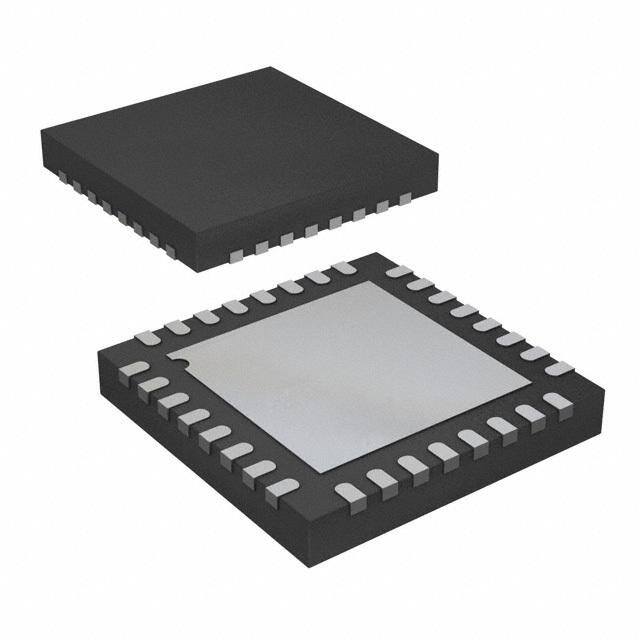
| 供应商器件封装 | 32-LFCSP-VQ(5x5) |
| 分辨率 | 8 bit |
| 包装 | 托盘 |
| 商标 | Analog Devices |
| 安装类型 | 表面贴装 |
| 安装风格 | SMD/SMT |
| 封装 | Tray |
| 封装/外壳 | 32-VFQFN 裸露焊盘,CSP |
| 封装/箱体 | LFCSP-32 |
| 工作温度 | -40°C ~ 85°C |
| 工厂包装数量 | 490 |
| 建立时间 | 11ns |
| 接口类型 | Parallel |
| 数据接口 | 串行 |
| 最大功率耗散 | 57 mW |
| 最大工作温度 | + 85 C |
| 最小工作温度 | - 40 C |
| 标准包装 | 1 |
| 电压参考 | Internal, External |
| 电压源 | 模拟和数字 |
| 电源电压-最大 | 3.6 V |
| 电源电压-最小 | 2.5 V |
| 积分非线性 | +/- 0.09 LSB |
| 稳定时间 | 11 ns |
| 系列 | AD9704 |
| 结构 | Segment |
| 转换器数 | 1 |
| 转换器数量 | 1 |
| 输出数和类型 | 2 电流 |
| 输出类型 | Current |
| 采样比 | 175 MSPs |
| 采样率(每秒) | 175M |


- 商务部:美国ITC正式对集成电路等产品启动337调查
- 曝三星4nm工艺存在良率问题 高通将骁龙8 Gen1或转产台积电
- 太阳诱电将投资9.5亿元在常州建新厂生产MLCC 预计2023年完工
- 英特尔发布欧洲新工厂建设计划 深化IDM 2.0 战略
- 台积电先进制程称霸业界 有大客户加持明年业绩稳了
- 达到5530亿美元!SIA预计今年全球半导体销售额将创下新高
- 英特尔拟将自动驾驶子公司Mobileye上市 估值或超500亿美元
- 三星加码芯片和SET,合并消费电子和移动部门,撤换高东真等 CEO
- 三星电子宣布重大人事变动 还合并消费电子和移动部门
- 海关总署:前11个月进口集成电路产品价值2.52万亿元 增长14.8%


PDF Datasheet 数据手册内容提取
8-/10-/12-/14-Bit, 175 MSPS TxDAC Digital-to-Analog Converters Data Sheet AD9704/AD9705/AD9706/AD9707 FEATURES The AD9704/AD9705/AD9706/AD9707 has an optional serial peripheral interface (SPI®) that provides a higher level of program- 175 MSPS update rate mability to enhance performance of the DAC. An adjustable Low power member of pin-compatible output, common-mode feature allows for easy interfacing to other TxDAC product family components that require common modes from 0 V to 1.2 V. Low power dissipation Edge-triggered input latches and a 1.0 V temperature-compensated 12 mW at 80 MSPS, 1.8 V band gap reference have been integrated to provide a complete, 50 mW at 175 MSPS, 3.3 V monolithic DAC solution. The digital inputs support 1.8 V and Wide supply voltage: 1.7 V to 3.6 V 3.3 V CMOS logic families. SFDR to Nyquist AD9707: 84 dBc at 5 MHz output PRODUCT HIGHLIGHTS AD9707: 83 dBc at 10 MHz output 1. Pin Compatible. The AD9704/AD9705/AD9706/AD9707 AD9707: 75 dBc at 20 MHz output line of TxDAC® converters is pin-compatible with the Adjustable full-scale current outputs: 1 mA to 5 mA AD9748/AD9740/AD9742/AD9744 TxDAC line (LFCSP On-chip 1.0 V reference package). CMOS-compatible digital interface 2. Low Power. Complete CMOS DAC operates on a single Common-mode output: adjustable 0 V to 1.2 V supply of 3.6 V down to 1.7 V, consuming 50 mW (3.3 V) Power-down mode <2 mW at 3.3 V (SPI controllable) and 12 mW (1.8 V). The DAC full-scale current can be Self-calibration reduced for lower power operation. Sleep and power-down Compact 32-lead LFCSP, RoHS compliant package modes are provided for low power idle periods. GENERAL DESCRIPTION 3. Self-Calibration. Self-calibration enables true 14-bit INL and DNL performance in the AD9707. The AD9704/AD9705/AD9706/AD9707 are the fourth-generation 4. Twos Complement/Binary Data Coding Support. Data family in the TxDAC series of high performance, CMOS digital-to- input supports twos complement or straight binary data analog converters (DACs). This pin-compatible, 8-/10-/12-/14-bit coding. resolution family is optimized for low power operation, while 5. Flexible Clock Input. A selectable high speed, single-ended, maintaining excellent dynamic performance. The AD9704/ and differential CMOS clock input supports 175 MSPS AD9705/AD9706/AD9707 family is pin-compatible with the conversion rate. AD9748/AD9740/AD9742/AD9744 family of TxDAC converters 6. Device Configuration. Device can be configured through and is specifically optimized for the transmit signal path of pin strapping, and SPI control offers a higher level of communication systems. All of the devices share the same programmability. interface, LFCSP package, and pinout, providing an upward or 7. Easy Interfacing to Other Components. Adjustable downward component selection path based on performance, common-mode output allows for easy interfacing to other resolution, and cost. The AD9704/AD9705/AD9706/AD9707 signal chain components that accept common-mode levels offers exceptional ac and dc performance, while supporting from 0 V to 1.2 V. update rates up to 175 MSPS. 8. On-Chip Voltage Reference. The AD9704/AD9705/AD9706/ The flexible power supply operating range of 1.7 V to 3.6 V and low AD9707 include a 1.0 V temperature-compensated band power dissipation of the AD9704/AD9705/AD9706/AD9707 parts gap voltage reference. make them well suited for portable and low power applications. 9. Industry-Standard 32-Lead LFCSP Package. Power dissipation of the AD9704/AD9705/AD9706/AD9707 can be reduced to 15 mW, with a small trade-off in performance, by lowering the full-scale current output. In addition, a power-down mode reduces the standby power dissipation to approximately 2.2 mW. Rev. D Document Feedback Information furnished by Analog Devices is believed to be accurate and reliable. However, no responsibility is assumed by Analog Devices for its use, nor for any infringements of patents or other One Technology Way, P.O. Box 9106, Norwood, MA 02062-9106, U.S.A. rights of third parties that may result from its use. Specifications subject to change without notice. No license is granted by implication or otherwise under any patent or patent rights of Analog Devices. Tel: 781.329.4700 ©2006–2017 Analog Devices, Inc. All rights reserved. Trademarks and registered trademarks are the property of their respective owners. Technical Support www.analog.com
AD9704/AD9705/AD9706/AD9707 Data Sheet TABLE OF CONTENTS Features .............................................................................................. 1 Terminology .................................................................................... 29 General Description ......................................................................... 1 Theory of Operation ...................................................................... 30 Product Highlights ........................................................................... 1 Serial Peripheral Interface ......................................................... 30 Revision History ............................................................................... 2 SPI Register Map ........................................................................ 32 Functional Block Diagram .............................................................. 4 SPI Register Descriptions .......................................................... 33 Specifications ..................................................................................... 5 Reference Operation .................................................................. 34 DC Specifications (3.3 V) ............................................................ 5 Reference Control Amplifier .................................................... 34 Dynamic Specifications (3.3 V) .................................................. 6 DAC Transfer Function ............................................................. 35 Digital Specifications (3.3 V) ...................................................... 7 Analog Outputs .......................................................................... 35 DC Specifications (1.8 V) ............................................................ 8 Adjustable Output Common Mode ......................................... 36 Dynamic Specifications (1.8 V) .................................................. 9 Digital Inputs .............................................................................. 36 Digital Specifications (1.8 V) .................................................... 10 Clock Input .................................................................................. 36 Timing Diagram ......................................................................... 10 DAC Timing ................................................................................ 36 Absolute Maximum Ratings .......................................................... 11 Power Dissipation....................................................................... 37 Thermal Characteristics ............................................................ 11 Self-Calibration ........................................................................... 38 ESD Caution ................................................................................ 11 Applications Information .............................................................. 40 Pin Configurations and Function Descriptions ......................... 12 Output Configurations .............................................................. 40 AD9707 ........................................................................................ 12 Differential Coupling Using a Transformer ............................... 40 AD9706 ........................................................................................ 13 Single-Ended Buffered Output Using an Op Amp ................ 40 AD9705 ........................................................................................ 14 Differential Buffered Output Using an Op Amp ................... 41 AD9704 ........................................................................................ 15 Evaluation Board ........................................................................ 41 Typical Performance Characteristics ........................................... 16 Outline Dimensions ....................................................................... 42 AD9707......................................................................................... 16 Ordering Guide .......................................................................... 42 AD9704, AD9705 and AD9706 .................................................. 23 REVISION HISTORY 11/2017—Rev. C to Rev. D Changes to Table 2 ............................................................................. 6 Changed CP-32-7 to CP-32-2 ...................................... Throughout Changes to Table 4 ............................................................................. 8 Updated Outline Dimensions ....................................................... 42 Changes to Table 5 ............................................................................. 9 Changes to Ordering Guide .......................................................... 42 Changes to Figure 3 and Table 9 ................................................... 12 Changes to Figure 4 and Table 10................................................. 13 9/2017—Rev. B to Rev. C Changes to Figure 5 and Table 11................................................. 14 Changed CP-32-2 to CP-32-7 ...................................... Throughout Changes to Figure 6 and Table 12................................................. 15 Changes to Table 9 .......................................................................... 12 Changes to Figure 15 and Figure 16............................................. 17 Changes to Table 10 ........................................................................ 13 Moved Figure 41 to Figure 24 Position........................................ 18 Changes to Table 11 ........................................................................ 14 Moved Figure 42 to Figure 25 Position and Moved Figure 43 to Changes to Table 12 ........................................................................ 15 Figure 26 Position ........................................................................... 19 Changes to Reference Operation Section .................................... 34 Changes to Figure 27 ...................................................................... 20 Updated Outline Dimensions ....................................................... 42 Changes to Figure 33 to Figure 35 ................................................ 21 Changes to Ordering Guide .......................................................... 42 Moved Figure 24 to Figure 41 Position........................................ 22 Moved Figure 25 to Figure 43 Position and Moved Figure 26 to 10/2011—Rev. A to Rev. B Figure 44 Position ........................................................................... 23 Changes to Features Section............................................................ 1 Changes to Figure 44 ...................................................................... 23 Changes to Table 1 ............................................................................ 5 Changes to Figure 57 ...................................................................... 26 Rev. D | Page 2 of 42
Data Sheet AD9704/AD9705/AD9706/AD9707 Changes to Figure 44 ...................................................................... 23 Changes to Figure 57 ...................................................................... 26 4/2007—Rev. 0 to Rev. A Changes to Figure 70 ...................................................................... 29 Changes to Features List ................................................................... 1 Changes to Serial Peripheral Interface Section ........................... 30 Changes to Product Highlights ....................................................... 1 Changes to Table 15 ........................................................................ 32 Changes to General Description ..................................................... 3 Deleted Table 23; Renumbered Sequentially ............................... 33 Changes to Table 3 ............................................................................ 6 Changes to Reference Operation Section and Reference Control Changes to Table 4 ............................................................................ 7 Amplifier Section ............................................................................ 34 Changes to Table 6 ............................................................................ 9 Changes to Adjustable Output Common Mode Section and Changes to Figure 17 and Figure 18 ............................................. 16 DAC Timing Section....................................................................... 36 Deleted Figure 29, Renumbered Sequentially ............................. 19 Added the Deskew Mode Section ................................................. 36 Changes to Figure 44 ...................................................................... 22 Deleted Figure 80; Renumbered Sequentially ............................. 36 Changes to Figure 57 Caption ....................................................... 25 Changed Sleep and Power-Down Operation (Pin Mode) Section Changes to Figure 73, Figure 75, and Figure 77 .......................... 31 to Sleep Operation (Pin Mode) Section ....................................... 38 Changes to Table 16 ........................................................................ 32 Changes to Sleep Operation (Pin Mode) Section ....................... 38 Replaced Single-Ended Buffered Output Using an Op Changes to Self-Calibration Section ............................................. 39 Amp Section .................................................................................... 40 Changes to Evaluation Board Section .......................................... 41 Changes to Figure 91 ...................................................................... 41 Added Exposed Pad Notation to Outline Dimensions .............. 42 Changes to Figure 93 ...................................................................... 44 Changes to Ordering Guide ........................................................... 42 Changes to Figure 96 ...................................................................... 47 Deleted Evaluation Board Schematics Section ............................ 43 Deleted Figure 92 to Figure 102 .................................................... 43 7/2006—Revision 0: Initial Version Rev. D | Page 3 of 42
AD9704/AD9705/AD9706/AD9707 Data Sheet FUNCTIONAL BLOCK DIAGRAM 1.7V TO 3.6V 1.0V REF AVDD ACOM 0.1µF AD9707 REFIO CURRENT SOURCE OTCM FS ADJ ARRAY 1.7V RSET TO CLKVDD IOUTA 3.6V CLKCOM SEGMENTED LSB IOUTB SWITCHES SWITCHES CLK+ PIN/SPI/RESET CLK– LATCHES SPI MODE/SDIO 1.7V3 .T6OV DVDD CMODE/SCLK DCOM DIGITAL INPUTS (DB13 TO DB0) SLEEP/CSB 05926-001 Figure 1. Rev. D | Page 4 of 42
Data Sheet AD9704/AD9705/AD9706/AD9707 SPECIFICATIONS DC SPECIFICATIONS (3.3 V) T to T , AVDD = 3.3 V, DVDD = 3.3 V, CLKVDD = 3.3 V, I = 2 mA, unless otherwise noted. MIN MAX OUTFS Table 1. AD9707 AD9706 AD9705 AD9704 Parameter Min Typ Max Min Typ Max Min Typ Max Min Typ Max Unit RESOLUTION 14 12 10 8 Bits DC ACCURACY1 Integral Nonlinearity (INL) ±1.4 ±6.0 ±0.41 ±1.48 ±0.10 ±0.36 ±0.03 ±0.09 LSB Precalibration Integral Nonlinearity (INL) ±0.9 ±0.30 ±0.10 LSB Postcalibration Differential Nonlinearity ±1.2 ±4.4 ±0.35 ±1.17 ±0.09 ±0.31 ±0.02 ±0.08 LSB (DNL) Precalibration Differential Nonlinearity ±0.4 ±0.13 ±0.03 LSB (DNL) Postcalibration ANALOG OUTPUT Offset Error −0.03 0 +0.03 −0.03 0 +0.03 −0.03 0 +0.03 −0.03 0 +0.03 % of FSR Gain Error (With External −2.7 −0.1 +2.7 −2.7 −0.1 +2.7 −2.7 −0.1 +2.7 −2.7 −0.1 +2.7 % of FSR Reference Gain Error (With Internal −2.7 −0.1 +2.7 −2.7 −0.1 +2.7 −2.7 −0.1 +2.7 −2.7 −0.1 +2.7 % of FSR Reference) Full-Scale Output Current2 1 2 5 1 2 5 1 2 5 1 2 5 mA Output Compliance Range −0.8 +0.8 −0.8 +0.8 −0.8 +0.8 −0.8 +0.8 V (From OTCM to IOUTA/IOUTB) Output Resistance 200 200 200 200 MΩ Output Capacitance 5 5 5 5 pF REFERENCE OUTPUT Reference Voltage 0.98 1.025 1.08 0.98 1.025 1.08 0.98 1.025 1.08 0.98 1.025 1.08 V Reference Output Current3 100 100 100 100 nA REFERENCE INPUT Input Compliance Range 0.1 1.25 0.1 1.25 0.1 1.25 0.1 1.25 V Reference Input Resistance 10 10 10 10 kΩ (Reference Powered Up) Reference Input Resistance 1 1 1 1 MΩ (Reference Powered Down) TEMPERATURE COEFFICIENTS Offset Drift 0 0 0 0 ppm of FSR/°C Gain Drift (Without Internal ±29 ±29 ±29 ±29 ppm of Reference) FSR/°C Gain Drift (With Internal ±40 ±40 ±40 ±40 ppm of Reference) FSR/°C Reference Voltage Drift ±25 ±25 ±25 ±25 ppm/°C POWER SUPPLY Supply Voltage AVDD 3.3 3.6 3.3 3.6 3.3 3.6 3.3 3.6 V DVDD 3.3 3.6 3.3 3.6 3.3 3.6 3.3 3.6 V CLKVDD 3.3 3.6 3.3 3.6 3.3 3.6 3.3 3.6 V Analog Supply Current (I ) 5.2 6.7 5.2 6.7 5.1 6.7 5.1 6.7 mA AVDD Digital Supply Current (I )4 5.9 6.6 5.4 6.6 5.0 6.6 4.6 6.6 mA DVDD Clock Supply Current (I )4 4.1 4.7 4.1 4.7 4.1 4.7 4.1 4.7 mA CLKVDD Power Dissipation4 50.2 57 48.5 57 46.9 57 45.5 57 mW Supply Current Sleep Mode 0.37 0.4 0.37 0.4 0.37 0.4 0.37 0.4 mA (I ) AVDD Rev. D | Page 5 of 42
AD9704/AD9705/AD9706/AD9707 Data Sheet AD9707 AD9706 AD9705 AD9704 Parameter Min Typ Max Min Typ Max Min Typ Max Min Typ Max Unit Supply Current Power-Down 0.7 7.5 0.7 7.5 0.7 7.5 0.7 7.5 µA Mode (I ) AVDD Supply Current Clock Power- 0.6 1 0.6 1 0.6 1 0.6 1 mA Down Mode (I )5 DVDD Supply Current Clock Power- 42.5 64 42.5 64 42.5 64 42.5 64 µA Down Mode (I )5 CLKVDD Power Supply Rejection Ratio −0.2 +0.03 +0.2 −0.2 +0.03 +0.2 −0.2 +0.03 +0.2 −0.2 +0.03 +0.2 % of (AVDD)6 FSR/V OPERATING RANGE −40 +85 −40 +85 −40 +85 −40 +85 °C 1 Measured at IOUTA, driving a virtual ground. 2 Normal full scale current, IOUTFS is 32 × the IREF current. 3 Use an external buffer amplifier with an input bias current <100 nA to drive any external load. 4 Measured at fCLOCK = 175 MSPS and fOUT = 1.0 MHz, using a differential clock. 5 Measured at fCLOCK = 100 MSPS and fOUT = 1.0 MHz, using a differential clock. 6 ± 5% power supply variation. DYNAMIC SPECIFICATIONS (3.3 V) T to T , AVDD = 3.3 V, DVDD = 3.3 V, CLKVDD = 3.3 V, I = 2 mA, differential transformer coupled output, 453 Ω differentially MIN MAX OUTFS terminated unless otherwise noted. Table 2. AD9707 AD9706 AD9705 AD9704 Parameter Min Typ Max Min Typ Max Min Typ Max Min Typ Max Unit DYNAMIC PERFORMANCE Maximum Output Update Rate, f 175 175 175 175 MSPS CLOCK Output Settling Time, t (to 0.1%)1 11 11 11 11 ns ST Output Propagation Delay, t 4 4 4 4 ns PD Glitch Impulse 5 5 5 5 pV-s Output Rise Time (10% to 90%)1 2.5 2.5 2.5 2.5 ns Output Fall Time (10% to 90%)1 2.5 2.5 2.5 2.5 ns AC LINEARITY Spurious-Free Dynamic Range to Nyquist f = 10 MSPS, f = 2.1 MHz 84 84 84 70 dBc CLOCK OUT f = 25 MSPS, f = 2.1 MHz 84 83 84 68 dBc CLOCK OUT f = 65 MSPS, f = 5.1 MHz 84 84 84 70 dBc CLOCK OUT f = 65 MSPS, f = 10.1 MHz 83 83 83 71 dBc CLOCK OUT f = 80 MSPS, f = 1.0 MHz 74 83 72 82 72 82 66 70 dBc CLOCK OUT f = 125 MSPS, f = 15.1 MHz 78 78 78 68 dBc CLOCK OUT f = 125 MSPS, f = 25.1 MHz 77 77 76 69 dBc CLOCK OUT f = 175 MSPS, f = 20.1 MHz 75 75 75 69 dBc CLOCK OUT f = 175 MSPS, f = 40.1 MHz 72 71 71 67 dBc CLOCK OUT Noise Spectral Density f = 175 MSPS, f = 6.0 MHz, −152 −152 −144 −136 dBc/Hz CLOCK OUT I = 2 mA OUTFS f = 175 MSPS, f = 6.0 MHz, −161 dBc/Hz CLOCK OUT I = 5 mA OUTFS f = 175 MSPS, f = 6.0 MHz, −146 dBc/Hz CLOCK OUT I = 1 mA OUTFS 1 Measured single-ended into 500 Ω load. Rev. D | Page 6 of 42
Data Sheet AD9704/AD9705/AD9706/AD9707 DIGITAL SPECIFICATIONS (3.3 V) T to T , AVDD = 3.3 V, DVDD = 3.3 V, CLKVDD = 3.3 V, I = 2 mA, unless otherwise noted. MIN MAX OUTFS Table 3. AD9707 AD9706 AD9705 AD9704 Parameter Min Typ Max Min Typ Max Min Typ Max Min Typ Max Unit DIGITAL INPUTS1 Logic 1 Voltage 2.1 3 2.1 3 2.1 3 2.1 3 V Logic 0 Voltage 0 0.9 0 0.9 0 0.9 0 0.9 V Logic 1 Current −10 +10 −10 +10 −10 +10 −10 +10 µA Logic 0 Current 10 10 10 10 µA Input Capacitance 5 5 5 5 pF Input Setup Time, t, +25°C 1.4 1.4 1.4 1.4 ns S Input Hold Time, t , +25°C 0.3 0.3 0.3 0.3 ns H Input Setup Time, t, −40°C to +85°C 1.6 1.6 1.6 1.6 ns S Input Hold Time, t , −40°C to +85°C 0.6 0.6 0.6 0.6 ns H Latch Pulse Width, t 2.8 2.8 2.8 2.8 ns LPW CLK INPUTS2 Input Voltage Range 0 3 0 3 0 3 0 3 V Common-Mode Voltage 0.75 1.5 2.25 0.75 1.5 2.25 0.75 1.5 2.25 0.75 1.5 2.25 V Differential Voltage 0.5 1.5 0.5 1.5 0.5 1.5 0.5 1.5 V 1 Includes CLK+ pin in single-ended clock input mode. 2 Applicable to CLK+ input and CLK− input when configured for differential clock input mode. Rev. D | Page 7 of 42
AD9704/AD9705/AD9706/AD9707 Data Sheet DC SPECIFICATIONS (1.8 V) T to T , AVDD = 1.8 V, DVDD = 1.8 V, CLKVDD = 1.8 V, I = 2 mA, unless otherwise noted. MIN MAX OUTFS Table 4. AD9707 AD9706 AD9705 AD9704 Parameter Min Typ Max Min Typ Max Min Typ Max Min Typ Max Unit RESOLUTION 14 12 10 8 Bits DC ACCURACY1 Integral Nonlinearity (INL) ±1.4 ±6.03 ±0.42 ±1.50 ±0.10 ±0.36 ±0.03 ±0.09 LSB Precalibration Differential Nonlinearity ±1.2 ±4.34 ±0.36 ±1.17 ±0.09 ±0.30 ±0.02 ±0.07 LSB (DNL) Precalibration ANALOG OUTPUT Offset Error −0.03 0 +0.03 −0.03 0 +0.03 −0.03 0 +0.03 −0.03 0 +0.03 % of FSR Gain Error (With Internal −2.7 −0.2 +2.7 −2.7 −0.2 +2.7 −2.7 −0.2 +2.7 −2.7 −0.2 +2.7 % of FSR Reference) Full-Scale Output Current2 1 2 2.5 1 2 2.5 1 2 2.5 1 2 2.5 mA Output Compliance Range −0.8 +0.8 −0.8 +0.8 −0.8 +0.8 −0.8 +0.8 V (With OTCM = AGND) Output Resistance 200 200 200 200 MΩ Output Capacitance 5 5 5 5 pF REFERENCE OUTPUT Reference Voltage 0.98 1.025 1.08 0.98 1.025 1.08 0.98 1.025 1.08 0.98 1.025 1.08 V Reference Output Current3 100 100 100 100 nA REFERENCE INPUT Input Compliance Range 0.1 1.25 0.1 1.25 0.1 1.25 0.1 1.25 V Reference Input Resistance 10 10 10 10 kΩ (Reference Powered Up) Reference Input Resistance 1 1 1 1 MΩ (External Reference) TEMPERATURE COEFFICIENTS Offset Drift 0 0 0 0 ppm of FSR/°C Gain Drift (Without Internal ±30 ±30 ±30 ±30 ppm of Reference) FSR/°C Gain Drift (With Internal ±60 ±60 ±60 ±60 ppm of Reference) FSR/°C Reference Voltage Drift ±25 ±25 ±25 ±25 ppm/°C POWER SUPPLY Supply Voltage AVDD 1.7 1.8 1.7 1.8 1.7 1.8 1.7 1.8 V DVDD 1.7 1.8 1.7 1.8 1.7 1.8 1.7 1.8 V CLKVDD 1.7 1.8 1.7 1.8 1.7 1.8 1.7 1.8 V Analog Supply Current 3.8 4.8 3.8 4.8 3.8 4.8 3.8 4.8 mA (I )4 AVDD Digital Supply Current 1.3 1.5 1.2 1.5 1.1 1.5 1.0 1.5 mA (IDVDD)4, 5 Clock Supply Current 1.3 1.5 1.3 1.5 1.3 1.5 1.3 1.5 mA (ICLKVDD)4, 5 Power Dissipation4, 5 11.5 13.2 11.3 13.2 11.1 13.2 11.0 13.2 mW Supply Current Sleep Mode 0.3 0.4 0.3 0.4 0.3 0.4 0.3 0.4 mA (I ) AVDD Supply Current Power-Down 5 6 5 6 5 6 5 6 µA Mode (I ) AVDD Supply Current Clock Power- 0.22 0.28 0.22 0.28 0.22 0.28 0.22 0.28 mA Down Mode (I )5 DVDD Supply Current Clock Power- 9.5 16 9.5 16 9.5 16 9.5 16 µA Down Mode (I )5 CLKVDD Rev. D | Page 8 of 42
Data Sheet AD9704/AD9705/AD9706/AD9707 AD9707 AD9706 AD9705 AD9704 Parameter Min Typ Max Min Typ Max Min Typ Max Min Typ Max Unit Power Supply Rejection −2 −0.1 +2 −2 −0.1 +2 −2 −0.1 +2 −2 −0.1 +2 % of Ratio (AVDD)6 FSR/V OPERATING RANGE −40 +85 −40 +85 −40 +85 −40 +85 °C 1 Measured at IOUTA, driving a virtual ground. 2 Nominal full-scale current, IOUTFS, is 32 × the IREF current. 3 Use an external buffer amplifier with an input bias current <100 nA to drive any external load. 4 Measured at IOUTFS = 1 mA. 5 Measured at fCLOCK = 80 MSPS and fOUT = 1 MHz, using a differential clock. 6 ±5% power supply variation. DYNAMIC SPECIFICATIONS (1.8 V) T to T , AVDD = 1.8 V, DVDD = 1.8 V, CLKVDD = 1.8 V, I = 1 mA, differential transformer coupled output, 453 Ω differentially MIN MAX OUTFS terminated unless otherwise noted. Table 5. AD9707 AD9706 AD9705 AD9704 Parameter Min Typ Max Min Typ Max Min Typ Max Min Typ Max Unit DYNAMIC PERFORMANCE Maximum Output Update Rate, f 125 125 125 125 MSPS CLOCK Output Settling Time, t , (to 0.1%)1 11 11 11 11 ns ST Output Propagation Delay (t ) 5.6 5.6 5.6 5.6 ns PD Glitch Impulse 5 5 5 5 pV-s Output Rise Time (10% to 90%)1 2.5 2.5 2.5 2.5 ns Output Fall Time (10% to 90%)1 2.5 2.5 2.5 2.5 ns AC LINEARITY Spurious-Free Dynamic Range to Nyquist f = 10 MSPS; f = 2.1 MHz 86 86 85 70 dBc CLOCK OUT f = 25 MSPS; f = 2.1 MHz 87 86 84 68 dBc CLOCK OUT f = 25 MSPS; f = 5.1 MHz 82 82 82 68 dBc CLOCK OUT f = 65 MSPS; f = 10.1 MHz 82 79 78 70 dBc CLOCK OUT f = 65 MSPS; f = 15.1 MHz 77 76 74 69 dBc CLOCK OUT f = 80 MSPS; f = 1.0 MHz 74 82 72 82 72 82 66 70 dBc CLOCK OUT f = 80 MSPS; f = 15.1 MHz 77 77 77 68 dBc CLOCK OUT f = 80 MSPS; f = 30.1 MHz 60 59 59 60 dBc CLOCK OUT Noise Spectral Density f = 80 MSPS; f = 10 MHz; −145 −144 −140 −128 dBc/Hz CLOCK OUT I = 1 mA OUTFS f = 80 MSPS; f = 10 MHz; −151 dBc/Hz CLOCK OUT I = 2 mA OUTFS 1 Measured single-ended into 500 Ω load. Rev. D | Page 9 of 42
AD9704/AD9705/AD9706/AD9707 Data Sheet DIGITAL SPECIFICATIONS (1.8 V) T to T , AVDD = 1.8 V, DVDD = 1.8 V, CLKVDD = 1.8 V, I = 1 mA, unless otherwise noted. MIN MAX OUTFS Table 6. AD9707 AD9706 AD9705 AD9704 Parameter Min Typ Max Min Typ Max Min Typ Max Min Typ Max Unit DIGITAL INPUTS1 Logic 1 Voltage 1.2 1.8 1.2 1.8 1.2 1.8 1.2 1.8 V Logic 0 Voltage 0 0.5 0 0.5 0 0.5 0 0.5 V Logic 1 Current −10 +10 −10 +10 −10 +10 −10 +10 µA Logic 0 Current +10 +10 +10 +10 µA Input Capacitance 5 5 5 5 pF Input Setup Time, t, 25°C 2.3 2.3 2.3 2.3 ns S Input Hold Time, t , 25°C 0 0 0 0 ns H Input Setup Time, t, −40°C to +85°C 2.4 2.4 2.4 2.4 ns S Input Hold Time, t , −40°C to +85°C 0.1 0.1 0.1 0.1 ns H Latch Pulse Width, t 6.2 6.2 6.2 6.2 ns LPW CLK INPUTS2 Input Voltage Range 0 1.8 0 1.8 0 1.8 0 1.8 V Common-Mode Voltage 0.4 0.9 1.3 0.4 0.9 1.3 0.4 0.9 1.3 0.4 0.9 1.3 V Differential Voltage 0.5 1.5 0.5 1.5 0.5 1.5 0.5 1.5 V 1 Includes CLK+ pin in single-ended clock input mode. 2 Applicable to CLK+ input and CLK– input when configured for differential clock input mode. TIMING DIAGRAM DB0 TO DB13 tS tH CLOCK tLPW tPD tST IOUTA OR IOUTB 0.1% 0.1% 05926-002 Figure 2. Timing Diagram Rev. D | Page 10 of 42
Data Sheet AD9704/AD9705/AD9706/AD9707 ABSOLUTE MAXIMUM RATINGS Stresses at or above those listed under Absolute Maximum Table 7. Ratings may cause permanent damage to the product. This is a Parameter Rating stress rating only; functional operation of the product at these AVDD to ACOM −0.3 V to +3.9 V or any other conditions above those indicated in the operational DVDD to DCOM −0.3 V to +3.9 V section of this specification is not implied. Operation beyond CLKVDD to CLKCOM −0.3 V to +3.9 V the maximum operating conditions for extended periods may ACOM to DCOM −0.3 V to +0.3 V affect product reliability. ACOM to CLKCOM −0.3 V to +0.3 V DCOM to CLKCOM −0.3 V to +0.3 V THERMAL CHARACTERISTICS AVDD to DVDD −3.9 V to +3.9 V Thermal impedance measurements were taken on a 4-layer board AVDD to CLKVDD −3.9 V to +3.9 V in still air, in accordance with EIA/JESD51-7. DVDD to CLKVDD −3.9 V to +3.9 V SLEEP to DCOM −0.3 V to DVDD + 0.3 V Table 8. Thermal Resistance Digital Inputs, MODE to DCOM −0.3 V to DVDD + 0.3 V Package Type θJA Unit IOUTA, IOUTB to ACOM −1.0 V to AVDD + 0.3 V 32-Lead LFCSP 32.5 °C/W REFIO, FS ADJ, OTCM to ACOM −0.3 V to AVDD + 0.3 V CLK+, CLK–, CMODE to CLKCOM −0.3 V to CLKVDD + 0.3 V ESD CAUTION Junction Temperature 150°C Storage Temperature Range −65°C to +150°C Lead Temperature (10 sec) 300°C Rev. D | Page 11 of 42
AD9704/AD9705/AD9706/AD9707 Data Sheet PIN CONFIGURATIONS AND FUNCTION DESCRIPTIONS AD9707 8910111213 (MSB)OMEEP/CSB PIN 1 DBDBDBDBDBDBDCSL INDICATOR 21098765 33322222 DB7 1 24 FS ADJ DB6 2 23 REFIO DVDD 3 AD9707 22 ACOM DB5 4 21 IOUTA DB4 5 TOP VIEW 20 IOUTB (Not to Scale) DB3 6 19 OTCM DB2 7 18 AVDD DB1 8 17 PIN/SPI/RESET 910111213141516 DB0 (LSB)DCOMCLKVDDCLK+CLK–CLKCOMMODE/SCLKMODE/SDIO C NOTES 1.IT IS RECOMMENDED THAT THE EXPOSED PAD BE TPPHLEAERRNFOME RAFMLOLARYN E CCNEOH.NANNECCETDE EDL TEOC TAR CICOAPLP AERN DG TRHOEURNMDAL 05926-003 Figure 3. AD9707 Pin Configuration Table 9. AD9707 Pin Function Descriptions Pin No. Mnemonic Description 28 to 32, 1, DB12 to DB1 Data Bit 12 to Data Bit 1. 2, 4 to 8 3 DVDD Digital Supply Voltage (1.7 V to 3.6 V). DVDD, AVDD, and CLKVDD must be at the same supply voltage. 9 DB0 (LSB) Least Significant Data Bit (LSB). 10, 26 DCOM Digital Common. 11 CLKVDD Clock Supply Voltage (1.7 V to 3.6 V). DVDD, AVDD, and CLKVDD must be at the same supply voltage. 12 CLK+ Positive Differential Clock Input. 13 CLK− Negative Differential Clock Input. 14 CLKCOM Clock Common. 15 CMODE/SCLK In pin mode, this pin selects the clock input type. Connect to CLKCOM for single-ended clock receiver (drive CLK+ and float CLK–). Connect to CLKVDD for differential receiver. In SPI mode, this pin is the serial data clock input. 16 MODE/SDIO In pin mode, this pin selects the input data format. Connect to DCOM for straight binary, and DVDD for twos complement. In SPI mode, this pin acts as SPI data input/output. 17 PIN/SPI/RESET Selects SPI Mode or Pin Mode Operation. Active high for pin mode operation and active low for SPI mode operation. Pulse high to reset SPI registers to default values. 18 AVDD Analog Supply Voltage (1.7 V to 3.6 V). DVDD, AVDD, and CLKVDD must be at the same supply voltage. 19 OTCM Adjustable Output Common Mode. Refer to the Theory of Operation section for details. 20 IOUTB Complementary DAC Current Output. Full-scale current is sourced when all data bits are 0s. 21 IOUTA DAC Current Output. Full-scale current is sourced when all data bits are 1s. 22 ACOM Analog Common. 23 REFIO Reference Input/Output. Serves as reference input when internal reference disabled. Serves as 1.0 V reference output when internal reference is activated. Requires a 0.1 μF capacitor to ACOM when internal reference is activated. 24 FS ADJ Full-Scale Current Output Adjust. 25 SLEEP/CSB In pin mode, active high powers down chip. In SPI mode, this pin is the serial port chip select (active low). 27 DB13 (MSB) Most Significant Data Bit (MSB). EPAD It is recommended that the exposed pad be thermally connected to a copper ground plane for enhanced electrical and thermal performance. Rev. D | Page 12 of 42
Data Sheet AD9704/AD9705/AD9706/AD9707 AD9706 67891011 (MSB)OMEEP/CSB BBBBBBCL PIN 1 DDDDDDDS INDICATOR 3231302928272625 DB5 1 24 FSADJ DB4 2 23 REFIO DVDD 3 AD9706 22 ACOM DB3 4 21 IOUTA DB2 5 TOP VIEW 20 IOUTB (Not to Scale) DB1 6 19 OTCM DB0 (LSB) 7 18 AVDD NC 8 17 PIN/SPI/RESET 910111213141516 CMD+–MKO NDCOCLKVDCLKCLKCLKCOMODE/SCLMODE/SDI C NOTES 1.NC = NO CONNECT. DO NOT CONNECTTO THIS PIN. 2. IT IS RECOMMENDED THAT THE EXPOSED PAD BE TPPHLEAERRNFOME RAFMLOLARYN E CCNEOH.NANNECCETDE EDL TEOC TAR CICOAPLP AERN DG TRHOEURNMDAL 05926-083 Figure 4. AD9706 Pin Configuration Table 10. AD9706 Pin Function Descriptions Pin No. Mnemonic Description 28 to 32, 1, DB10 to DB1 Data Bit 10 to Data Bit 1. 2, 4 to 6 3 DVDD Digital Supply Voltage (1.7 V to 3.6 V). DVDD, AVDD, and CLKVDD must be at the same supply voltage. 7 DB0 (LSB) Least Significant Data Bit (LSB). 8, 9 NC No Connect. 10, 26 DCOM Digital Common. 11 CLKVDD Clock Supply Voltage (1.7 V to 3.6 V). DVDD, AVDD, and CLKVDD must be at the same supply voltage. 12 CLK+ Positive Differential Clock Input. 13 CLK− Negative Differential Clock Input. 14 CLKCOM Clock Common. 15 CMODE/SCLK In pin mode, this pin selects the clock input type. Connect to CLKCOM for single-ended clock receiver (drive CLK+ and float CLK–). Connect to CLKVDD for differential receiver. In SPI mode, this pin is the serial data clock input. 16 MODE/SDIO In pin mode, this pin selects the input data format. Connect to DCOM for straight binary, and DVDD for twos complement. In SPI mode, this pin acts as SPI data input/output. 17 PIN/SPI/RESET Selects SPI Mode or Pin Mode Operation. Active high for pin mode operation, and active low for SPI mode operation. Pulse high to reset SPI registers to default values. 18 AVDD Analog Supply Voltage (1.7 V to 3.6 V). DVDD, AVDD, and CLKVDD must be at the same supply voltage. 19 OTCM Adjustable Output Common Mode. Refer to the Theory of Operation section for details. 20 IOUTB Complementary DAC Current Output. Full-scale current is sourced when all data bits are 0s. 21 IOUTA DAC Current Output. Full-scale current is sourced when all data bits are 1s. 22 ACOM Analog Common. 23 REFIO Reference Input/Output. Serves as reference input when internal reference disabled. Serves as 1.0 V reference output when internal reference is activated. Requires a 0.1 µF capacitor to ACOM when internal reference is activated. 24 FS ADJ Full-Scale Current Output Adjust. 25 SLEEP/CSB In pin mode, active high powers down chip. In SPI mode, this pin is the serial port chip select (active low). 27 DB11 (MSB) Most Significant Data Bit (MSB). EPAD It is recommended that the exposed pad be thermally connected to a copper ground plane for enhanced electrical and thermal performance. Rev. D | Page 13 of 42
AD9704/AD9705/AD9706/AD9707 Data Sheet AD9705 B B) S S C 456789 (MOMEEP/ PIN 1 DBDBDBDBDBDBDCSL INDICATOR 21098765 33322222 DB3 1 24 FSADJ DB2 2 23 REFIO DVDD 3 AD9705 22 ACOM DB1 4 21 IOUTA TOP VIEW DB0 (LSB) 5 20 IOUTB (Not to Scale) NC 6 19 OTCM NC 7 18 AVDD NC 8 17 PIN/SPI/RESET 910111213141516 CMD+–MKO NDCOCLKVDCLKCLKCLKCOMODE/SCLMODE/SDI C NOTES 1.NC = NO CONNECT. DO NOT CONNECTTO THIS PIN. 2. IT IS RECOMMENDED THAT THE EXPOSED PAD BE TPPHLEAERRNFOME RAFMLOLARYN E CCNEOH.NANNECCETDE EDL TEOC TAR CICOAPLP AERN DG TRHOEURNMDAL 05926-085 Figure 5. AD9705 Pin Configuration Table 11. AD9705 Pin Function Descriptions Pin No. Mnemonic Description 28 to 32, DB8 to DB1 Data Bit 8 to Data Bit 1. 1, 2, 4 3 DVDD Digital Supply Voltage (1.7 V to 3.6 V). DVDD, AVDD, and CLKVDD must be at the same supply voltage. 5 DB0 (LSB) Least Significant Data Bit (LSB). 6 to 9 NC No Connect. 10, 26 DCOM Digital Common. 11 CLKVDD Clock Supply Voltage (1.7 V to 3.6 V). DVDD, AVDD, and CLKVDD must be at the same supply voltage. 12 CLK+ Positive Differential Clock Input. 13 CLK− Negative Differential Clock Input. 14 CLKCOM Clock Common. 15 CMODE/SCLK In pin mode, this pin selects the clock input type. Connect to CLKCOM for single-ended clock receiver (drive CLK+ and float CLK–). Connect to CLKVDD for differential receiver. In SPI mode, this pin is the serial data clock input. 16 MODE/SDIO In pin mode, this pin selects the input data format. Connect to DCOM for straight binary, and DVDD for twos complement. In SPI mode, this pin acts as SPI data input/output. 17 PIN/SPI/RESET Selects SPI Mode or Pin Mode Operation. Active high for pin mode operation and active low for SPI mode operation. Pulse high to reset SPI registers to default values. 18 AVDD Analog Supply Voltage (1.7 V to 3.6 V). DVDD, AVDD, and CLKVDD must be at the same supply voltage. 19 OTCM Adjustable Output Common Mode. Refer to the Theory of Operation section for details. 20 IOUTB Complementary DAC Current Output. Full-scale current is sourced when all data bits are 0s. 21 IOUTA DAC Current Output. Full-scale current is sourced when all data bits are 1s. 22 ACOM Analog Common. 23 REFIO Reference Input/Output. Serves as reference input when internal reference disabled. Serves as 1.0 V reference output when internal reference is activated. Requires a 0.1 µF capacitor to ACOM when internal reference is activated. 24 FS ADJ Full-Scale Current Output Adjust. 25 SLEEP/CSB In pin mode, active high powers down chip. In SPI mode, this pin is the serial port chip select (active low). 27 DB9 (MSB) Most Significant Data Bit (MSB). EPAD It is recommended that the exposed pad be thermally connected to a copper ground plane for enhanced electrical and thermal performance. Rev. D | Page 14 of 42
Data Sheet AD9704/AD9705/AD9706/AD9707 AD9704 B B) S S C 234567 (MOMEEP/ PIN 1 DBDBDBDBDBDBDCSL INDICATOR 21098765 33322222 DB1 1 24 FSADJ DB0 (LSB) 2 23 REFIO DVDD 3 AD9704 22 ACOM NC 4 21 IOUTA NC 5 TOP VIEW 20 IOUTB (Not to Scale) NC 6 19 OTCM NC 7 18 AVDD NC 8 17 PIN/SPI/RESET 910111213141516 CMD+–MKO NDCOCLKVDCLKCLKCLKCOMODE/SCLMODE/SDI C NOTES 1.NC = NO CONNECT. DO NOT CONNECTTO THIS PIN. 2. IT IS RECOMMENDED THAT THE EXPOSED PAD BE TPPHLEAERRNFOME RAFMLOLARYN E CCNEOH.NANNECCETDE EDL TEOC TAR CICOAPLP AERN DG TRHOEURNMDAL 05926-084 Figure 6. AD9704 Pin Configuration Table 12. AD9704 Pin Function Descriptions Pin No. Mnemonic Description 28 to 32, 1 DB6 to DB1 Data Bit 6 to Data Bit 1. 2 DB0 (LSB) Least Significant Data Bit (LSB). 3 DVDD Digital Supply Voltage (1.7 V to 3.6 V). DVDD, AVDD, and CLKVDD must be at the same supply voltage. 4 to 9 NC No Connect. 10, 26 DCOM Digital Common. 11 CLKVDD Clock Supply Voltage (1.7 V to 3.6 V). DVDD, AVDD, and CLKVDD must be at the same supply voltage. 12 CLK+ Positive Differential Clock Input. 13 CLK− Negative Differential Clock Input. 14 CLKCOM Clock Common. 15 CMODE/SCLK In pin mode, this pin selects the clock input type. Connect to CLKCOM for single-ended clock receiver (drive CLK+ and float CLK−). Connect to CLKVDD for differential receiver. In SPI mode, this pin is the serial data clock input. 16 MODE/SDIO In pin mode, this pin selects the input data format. Connect to DCOM for straight binary, and DVDD for twos complement. In SPI mode, this pin acts as SPI data input/output. 17 PIN/SPI/RESET Selects SPI Mode or Pin Mode Operation. Active high for pin mode operation and active low for SPI mode operation. Pulse high to reset SPI registers to default values. 18 AVDD Analog Supply Voltage (1.7 V to 3.6 V). DVDD, AVDD, and CLKVDD must be at the same supply voltage. 19 OTCM Adjustable Output Common Mode. Refer to the Theory of Operation section for details. 20 IOUTB Complementary DAC Current Output. Full-scale current is sourced when all data bits are 0s. 21 IOUTA DAC Current Output. Full-scale current is sourced when all data bits are 1s. 22 ACOM Analog Common. 23 REFIO Reference Input/Output. Serves as reference input when internal reference disabled. Serves as 1.0 V reference output when internal reference is activated. Requires a 0.1 µF capacitor to ACOM when internal reference is activated. 24 FS ADJ Full-Scale Current Output Adjust. 25 SLEEP/CSB In pin mode, active high powers down chip. In SPI mode, this pin is the serial port chip select (active low). 27 DB7 (MSB) Most Significant Data Bit (MSB). EPAD It is recommended that the exposed pad be thermally connected to a copper ground plane for enhanced electrical and thermal performance. Rev. D | Page 15 of 42
AD9704/AD9705/AD9706/AD9707 Data Sheet TYPICAL PERFORMANCE CHARACTERISTICS AD9707 VDD = 3.3 V, I = 2 mA, unless otherwise noted. OUTFS 95 95 fCLOCK = 10MSPS 90 90 fCLOCK = 65MSPS 85 85 80 80 c) 75 c) 75 B B R (d 70 fCLOCK = 175MSPS R (d 70 D D F F S 65 S 65 60 fCLOCK = 125MSPS 60 55 55 50 50 45 45 1 fOUT1 (0MHz) 100 05926-005 0 5 10 15 20 25fO3U0T (M3H5z)40 45 50 55 60 65 05926-008 Figure 7. SFDR vs. fOUT Figure 10. SFDR vs. fOUT @ 125 MSPS 95 95 90 90 85 85 80 80 Bc) 75 Bc) 75 R (d 70 R (d 70 D D SF 65 SF 65 60 60 55 55 50 50 45 45 0 1 2fOUT (MHz)3 4 5 05926-006 0 10 20 30 fOU4T0 (MHz5)0 60 70 80 05926-009 Figure 8. SFDR vs. fOUT @ 10 MSPS Figure 11. SFDR vs. fOUT @ 175 MSPS 95 95 90 90 85 85 80 80 IOUTFS = 5mA Bc) 75 Bc) 75 IOUTFS = 2mA d d DR ( 70 DR ( 70 IOUTFS = 1mA F F S 65 S 65 60 60 55 55 50 50 45 45 0 5 10 1f5OUT (MH2z0) 25 30 35 05926-007 0 10 20 30 fOU4T0 (MHz5)0 60 70 80 05926-010 Figure 9. SFDR vs. fOUT @ 65 MSPS Figure 12. SFDR vs. fOUT and IOUTFS @ 175 MSPS Rev. D | Page 16 of 42
Data Sheet AD9704/AD9705/AD9706/AD9707 95 –120 90 –125 85 –130 80 –135 SFDR (dBc) 677505 OTCM = 0VOTCM = 0.3V NSD (dBc/Hz) ––114450 1mA 2mA OTCM = 1.2V –150 60 5mA 55 –155 50 –160 45 –165 0 10 20 30 fOU4T0 (MHz5)0 60 70 80 05926-011 0 10 20 3F0REQU4E0NCY (5M0Hz) 60 70 80 05926-116 Figure 13. SFDR vs. fOUT and OTCM @ 175 MSPS Figure 16. NSD vs. fOUT and IOUTFS @ 175 MSPS 95 95 90 fCLOCK = 65MSPS 90 85 85 fCLOCK = 75MSPS 80 fCLOCK = 125MSPS 80 fCLOCK = 175MSPS SFDR (dBc) 677505 fCLOCK = 175MSPS IMD (dBc) 677505 fCLOCK = 125MSPS 60 60 55 55 50 50 45–10 –8 –6AOUT (dBFS–)4 –2 0 05926-012 450 10 20 3L0OWER40 fOUT (5M0Hz) 60 70 80 05926-015 Figure 14. SFDR vs. AOUT and fCLOCK at fOUT = fCLOCK/5 Figure 17. Dual-Tone IMD vs. Lower fOUT and fCLOCK @ 0 dBFS –125 95 90 –130 +25°C 85 –135 80 +85°C SD (dBc/Hz) ––114450 65MSPS 125MSPS IMD (dBc) 677505 N 175MSPS 60 –40°C –150 55 –155 50 –1600 10 20 3F0REQU4E0NCY (5M0Hz) 60 70 80 05926-115 450 10 20 3L0OWER40 fOUT (5M0Hz) 60 70 80 05926-016 Figure 15. NSD vs. fOUT and fCLOCK @ 0 dBFS Figure 18. Dual-Tone IMD vs. Lower fOUT and Temperature at 0 dBFS, 175 MSPS Rev. D | Page 17 of 42
AD9704/AD9705/AD9706/AD9707 Data Sheet 0.6 1.0 0.5 0.5 0.4 0.3 B) 0 SB) L (LS NL (L 0.2 N D I –0.5 0.1 0 –1.0 –0.1 –1.50 5000 CODE10000 15000 05926-017 –0.2 0 5000 CODE 10000 15000 05926-087 Figure 19. Typical Uncalibrated INL Figure 22. Typical Calibrated DNL 0.6 95 90 0.4 85 0.2 80 –40°C SB) 0 dBc) 75 L (L DR ( 70 +25°C +85°C DN –0.2 SF 65 60 –0.4 55 –0.6 50 –0.80 5000 CODE10000 15000 05926-018 450 10 20 30 fOU4T0 (MHz5)0 60 70 80 05926-019 Figure 20. Typical Uncalibrated DNL Figure 23. SFDR vs. fOUT and Temperature @ 175 MSPS 0.6 –10 fCLOCK = 78MSPS 0.4 –20 fOSUFTD R= 1=5 8.00MdBHcz –30 AMPLITUDE = 0dBFS 0.2 m) –40 0 dB –50 SB) DE( NL (L–0.2 NITU –60 I G –70 –0.4 A M –80 –0.6 –90 –0.8 –100 –1.00 5000 CODE10000 15000 05926-086 –1101 6 11 FR1E6QUENC21Y (MHz)26 31 36 05926-039 Figure 21. Typical Calibrated INL Figure 24. Single-Tone SFDR Rev. D | Page 18 of 42
Data Sheet AD9704/AD9705/AD9706/AD9707 –10 –10 –20 fCfLOOUCTK1 == 1758.M0MSPHSz –20 fCfLOOUCTK1 == 1758.M0MSPHSz –30 fOSUFT2D R= 1=5 7.47MdBHcz –30 ffOOUUTT23 == 1155..48MMHHzz m) –40 AMPLITUDE = 0dBFS m) –40 fOSUFT4D R= 1=6 7.27MdBHcz B B AMPLITUDE = 0dBFS d –50 d –50 ( ( E E D D U –60 U –60 T T NI NI G –70 G –70 A A M M –80 –80 –90 –90 –100 –100 –1101 6 11 FR1E6QUEN2C1Y(MHz2)6 31 36 05926-038 –1101 6 11 FR1E6QUENC21Y(MHz2)6 31 36 05926-040 Figure 25. Dual-Tone SFDR Figure 26. Four-Tone SFDR Rev. D | Page 19 of 42
AD9704/AD9705/AD9706/AD9707 Data Sheet VDD = 1.8 V, I = 1 mA, unless otherwise noted. OUTFS 95 95 10MSPS 90 90 65MSPS 85 85 80 80 IOUTFS = 1mA c) 75 c) 75 dB 80MSPS dB R ( 70 R ( 70 D D SF 65 SF 65 IOUTFS = 2mA 60 60 55 55 50 50 125MSPS 45 45 1 FREQUE1N0CY (MHz) 100 05926-023 0 5 10 1f5OUT (MH2z0) 25 30 35 05926-027 Figure 27. SFDR vs. fOUT Figure 30. SFDR vs. fOUT and IOUTFS at 65 MSPS 95 95 90 90 85 85 80 80 Bc) 75 Bc) 75 IOUTFS = 1mA d d R ( 70 R ( 70 D D SF 65 SF 65 IOUTFS = 2mA 60 60 55 55 50 50 45 45 0 1 2fOUT (MHz)3 4 5 05926-024 0 5 10 15 fOUT2 (0MHz) 25 30 35 40 05926-028 Figure 28. SFDR vs. fOUT at 10 MSPS Figure 31. SFDR vs. fOUT and IOUTFS at 80 MSPS 95 95 90 90 85 85 80 80 fCLOCK = 80MSPS Bc) 75 Bc) 75 SFDR (d 6750 SFDR (d 6750 fCLOCK = 65MSPS 60 60 55 55 50 50 45 45 0 5 10 15 fOUT2 (0MHz) 25 30 35 40 05926-026 –10 –8 –A6OUT (dBFS–)4 –2 0 05926-029 Figure 29. SFDR vs. fOUT at 80 MSPS Figure 32. SFDR vs. AOUT at fOUT = fCLOCK/5 Rev. D | Page 20 of 42
Data Sheet AD9704/AD9705/AD9706/AD9707 –115 95 –120 90 85 –125 80 –130 125MSPS, 1mA –40°C D (dBc/Hz) ––114305 80MSPS, 1mA65MSPS, 1mA MD (dBc) 7705 +85°C NS I 65 –145 +25°C 60 125MSPS, 2mA –150 55 80MSPS, 2mA –155 65MSPS, 2mA 50 –1600 10 20 FRE3Q0UENCY4 (0MHz) 50 60 70 05926-133 450 5 10 L1O5WERf2O0UT (MH2z5) 30 35 40 05926-033 Figure 33. NSD vs. fOUT, fCLOCK, and IOUTFS at 0 dBFS Figure 36. Dual-Tone IMD vs. Lower fOUT and Temperature at 80 MSPS, IOUTFS = 1 mA and 0 dBFS 95 95 90 90 +25°C 85 85 80 80 65MSPS –40°C Bc) 75 Bc) 75 D (d 70 25MSPS 80MSPS D (d 70 M M I 65 I 65 60 60 55 55 +80°C 125MSPS 50 50 45 45 0 10 20FREQUE3N0CY (MHz)40 50 60 05926-134 0 5 10 L1O5WERf2O0UT (MH2z5) 30 35 40 05926-034 Figure 34. Dual-Tone IMD vs. Lower fOUT at IOUTFS = 1 mA and 0 dBFS Figure 37. Dual-Tone IMD vs. Lower fOUT and Temperature at 80 MSPS, IOUTFS = 2 mA and 0 dBFS 95 1.0 90 85 0.5 80 c/Hz) 75 65MSPS B) 0.0 D (dB 70 25MSPS 80MSPS L (LS IM 65 IN –0.5 60 55 –1.0 50 125MSPS 45 0 10 20FREQUE3N0CY (MHz)40 50 60 05926-135 –1.50 5000 CODE10000 15000 05926-035 Figure 35. Dual-Tone IMD vs. Lower fOUT at IOUTFS = 2 mA and 0 dBFS Figure 38. Typical Uncalibrated INL Rev. D | Page 21 of 42
AD9704/AD9705/AD9706/AD9707 Data Sheet 0.6 –10 –20 fCLOCK = 78MSPS 0.4 fOUT1 = 15.0MHz –30 fOUT2 = 15.4MHz SFDR = 74dBc 0.2 m) –40 AMPLITUDE = 0dBFS B SB) 0 E (d –50 DNL (L –0.2 GNITUD ––6700 A M –0.4 –80 –90 –0.6 –100 –0.80 5000 CODE10000 15000 05926-036 –1101 6 11 FR1E6QUENC21Y (MHz2)6 31 36 05926-021 Figure 39. Typical Uncalibrated DNL Figure 42. Dual-Tone SFDR 95 –10 90 –20 fCLOCK = 78MSPS fOUT1 = 15.0MHz 85 –40°C –30 ffOOUUTT23 == 1155..48MMHHzz 80 m) –40 fSOFUDTR4 == 1669.d2BMcHz c) 75 dB –50 AMPLITUDE = 0dBFS dB E ( R ( 70 +85°C UD –60 D T SF 65 +25°C GNI –70 A M 60 –80 55 –90 50 –100 450 5 10 15 fOUT2 (0MHz) 25 30 35 40 05926-037 –1101 6 11 FR1E6QUENC21Y (MHz2)6 31 36 05926-022 Figure 40. SFDR vs. Temperature at 80 MSPS Figure 43. Four-Tone SFDR –10 –20 fCLOCK = 78MSPS fOUT = 15.0MHz SFDR = 79dBc –30 AMPLITUDE = 0dBFS m) –40 B d –50 E ( D U –60 T NI G –70 A M –80 –90 –100 –1101 6 11 FR1E6QUENC21Y (MHz2)6 31 36 05926-020 Figure 41. Single-Tone SFDR Rev. D | Page 22 of 42
Data Sheet AD9704/AD9705/AD9706/AD9707 AD9704, AD9705 AND AD9706 VDD = 3.3 V, I = 2 mA, unless otherwise noted. OUTFS –115 0.01 –120 –125 8-BIT –130 D (dBc/Hz) ––113450 10-BIT NL (LSB) 0 NS 12-BIT I –145 14-BIT –150 –155 –160 –0.01 0 20 f4O0UT (MHz) 60 80 05926-144 0 200 400 CODE600 800 1000 05926-044 Figure 44. AD9704/AD9705/AD9706/AD9707 NSD vs. fOUT at 0 dBFS, Figure 47. AD9705 Typical Uncalibrated INL 175 MSPS 0.03 0.01 0.02 B) 0.01 B) NL (LS NL (LS 0 I 0 D –0.01 –0.02 –0.01 0 50 100 CODE150 200 250 05926-043 0 200 400 CODE600 800 1000 05926-045 Figure 45. AD9704 Typical Uncalibrated INL Figure 48. AD9705 Typical Uncalibrated DNL 0.01 0.3 0.2 0 0.1 0 B) B) S S NL (L –0.01 NL (L –0.1 D I –0.2 –0.02 –0.3 –0.4 –0.03 –0.5 0 50 100 CODE150 200 250 05926-042 0 1000 2C0O0D0E 3000 4000 05926-046 Figure 46. AD9704 Typical Uncalibrated DNL Figure 49. AD9706 Typical Uncalibrated INL Rev. D | Page 23 of 42
AD9704/AD9705/AD9706/AD9707 Data Sheet 0.01 –10 –20 ffCOLUOTC =K 1 =5 .708MMHSzPS SFDR = 75dBc 0 –30 AMPLITUDE = 0dBFS –40 m) B SB) –0.01 E (d –50 DNL (L –0.02 GNITUD ––6700 A M –80 –0.03 –90 –100 –0.04 –110 0 1000 2C0O00DE 3000 4000 05926-047 1 6 11 FR1E6QUENC21Y (MHz2)6 31 36 05926-050 Figure 50. AD9706 Typical Uncalibrated DNL Figure 53. AD9705 Single-Tone SFDR –10 –10 –20 ffCOLUOTC =K 1 =5 .708MMHSzPS –20 ffCOLUOTC1 K= =1 57.80MMSHPzS –30 SAFMDPRL I=T U67DdEB =c 0dBFS –30 fSOFUDTR2 == 1753.d4BMcHz m) –40 m) –40 AMPLITUDE = 0dBFS UDE (dB ––5600 UDE (dB ––5600 GNIT –70 GNIT –70 A A M –80 M –80 –90 –90 –100 –100 –1101 6 11 FR1E6QUENC21Y (MHz2)6 31 36 05926-048 –1101 6 11 FR1E6QUENC21Y (MHz2)6 31 36 05926-061 Figure 51. AD9704Single-Tone SFDR Figure 54. AD9705 Dual-Tone SFDR –10 –10 –20 ffCOLUOTC1 K= =1 57.80MMSHPzS –20 ffCOLUOTC1 K= =1 57.80MMSHPzS –30 fSOFUDTR2 == 1657.d4BMcHz –30 SAFMDPRL I=T U77DdEB =c 0dBFS AMPLITUDE = 0dBFS m) –40 m) –40 E (dB –50 E (dB –50 UD –60 UD –60 GNIT –70 GNIT –70 A A M –80 M –80 –90 –90 –100 –100 –1101 6 11 FR1E6QUENC21Y (MHz2)6 31 36 05926-049 –1101 6 11 FR1E6QUENC21Y (MHz2)6 31 36 05926-062 Figure 52. AD9704 Dual-Tone SFDR Figure 55. AD9706 Single-Tone SFDR Rev. D | Page 24 of 42
Data Sheet AD9704/AD9705/AD9706/AD9707 –10 –20 fCLOCK = 78MSPS fOUT1 = 15.0MHz –30 fOUT2 = 15.4MHz SFDR = 77dBc AMPLITUDE = 0dBFS m) –40 B d –50 E ( D U –60 T NI G –70 A M –80 –90 –100 –1101 6 11 FR1E6QUENC21Y (MHz2)6 31 36 05926-063 Figure 56. AD9706Dual-Tone SFDR Rev. D | Page 25 of 42
AD9704/AD9705/AD9706/AD9707 Data Sheet VDD = 1.8 V, I = 1 mA, unless otherwise noted. OUTFS –115 0.08 –120 0.06 –125 8-BIT 0.04 –130 Hz) NSD (dBc/ ––113450 12-BIT 10-BIT NL (LSB) 0.020 –145 I –0.02 14-BIT –150 –0.04 –155 –0.06 –160 0 5 10 1f5OUT (MH2z0) 25 30 35 05926-157 –0.080 200 400 CODE600 800 1000 05926-067 Figure 57. AD9704/AD9705/AD9706/AD9707 NSD vs. fOUT at 0 dBFS, 80 MSPS Figure 60. AD9705 Typical Uncalibrated INL 0.04 0.02 0 0.03 –0.02 0.02 INL (LSB) 0.01 DNL (LSB) ––00..0064 0 –0.08 –0.01 –0.10 –0.020 50 100 CODE150 200 250 05926-065 –0.120 200 400 CODE600 800 1000 05926-068 Figure 58. AD9704 Typical Uncalibrated INL Figure 61. AD9705Typical Uncalibrated DNL 0.01 0.3 0.2 0 0.1 0 B) B) S S NL (L –0.01 NL (L –0.1 D I –0.2 –0.02 –0.3 –0.4 –0.030 50 100 CODE150 200 250 05926-066 –0.50 1000 2C0O0D0E 3000 4000 05926-069 Figure 59. AD9704 Typical Uncalibrated DNL Figure 62. AD9706 Typical Uncalibrated INL Rev. D | Page 26 of 42
Data Sheet AD9704/AD9705/AD9706/AD9707 0.1 –10 –20 fCLOCK = 78MSPS fOUT = 15.0MHz SFDR = 73dBc 0 –30 AMPLITUDE = 0dBFS m) –40 B SB) –0.1 E (d –50 DNL (L –0.2 GNITUD ––6700 A M –80 –0.3 –90 –100 –0.40 1000 2C0O0D0E 3000 4000 05926-070 –1101 6 11 FR1E6QUENC21Y (MHz2)6 31 36 05926-073 Figure 63. AD9706 Typical Uncalibrated DNL Figure 66. AD9705 Single-Tone SFDR –10 –10 –20 ffOCLUOTC =K 1 =5 .708MMHSzPS –20 ffCOLUOTC1 K= =1 57.80MMSHPzS –30 SFDR = 67dBc –30 fOUT2 = 15.4MHz AMPLITUDE = 0dBFS SFDR = 71dBc AMPLITUDE = 0dBFS m) –40 m) –40 B B d –50 d –50 E ( E ( UD –60 UD –60 T T NI NI G –70 G –70 A A M M –80 –80 –90 –90 –100 –100 –1101 6 11 FR1E6QUENC21Y (MHz2)6 31 36 05926-071 –1101 6 11 FR1E6QUENC21Y (MHz2)6 31 36 05926-074 Figure 64. AD9704Single-Tone SFDR Figure 67. AD9705 Dual-Tone SFDR –10 –10 –20 ffCOLUOTC1 K= =1 57.80MMSHPzS –20 ffCOLUOTC=K 1 =5 .708MMHSzPS –30 fOUT2 = 15.4MHz –30 SFDR = 73dBc SFDR = 67dBc AMPLITUDE = 0dBFS AMPLITUDE = 0dBFS m) –40 m) –40 B B d –50 d –50 E ( E ( UD –60 UD –60 T T NI NI G –70 G –70 A A M M –80 –80 –90 –90 –100 –100 –1101 6 11 FR1E6QUENC21Y (MHz2)6 31 36 05926-072 –1101 6 11 FR1E6QUENC21Y (MHz2)6 31 36 05926-075 Figure 65. AD9704 Dual-Tone SFDR Figure 68. AD9706 Single-Tone SFDR Rev. D | Page 27 of 42
AD9704/AD9705/AD9706/AD9707 Data Sheet –10 –20 fCLOCK = 78MSPS fOUT1 = 15.0MHz –30 fOUT2 = 15.4MHz SFDR = 73dBc AMPLITUDE = 0dBFS m) –40 B d –50 E ( D U –60 T NI G –70 A M –80 –90 –100 –1101 6 11 FR1E6QUENC21Y (MHz2)6 31 36 05926-076 Figure 69. AD9706 Dual-Tone SFDR Rev. D | Page 28 of 42
Data Sheet AD9704/AD9705/AD9706/AD9707 TERMINOLOGY Linearity Error (Integral Nonlinearity or INL) Power Supply Rejection INL is defined as the maximum deviation of the actual analog Power supply rejection is the maximum change in the full-scale output from the ideal output, determined by a straight line output as the supplies are varied from nominal to minimum drawn from zero to full scale. and maximum specified voltages. Differential Nonlinearity (DNL) Settling Time DNL is the measure of the variation in analog value, normalized Settling time is the time required for the output to reach and to full scale, associated with a 1 LSB change in digital input code. remain within a specified error band about its final value, measured from the start of the output transition. Monotonicity A digital-to-analog converter is monotonic if the output either Glitch Impulse increases or remains constant as the digital input increases. Asymmetrical switching times in a DAC give rise to undesired output transients that are quantified by a glitch impulse. It is Offset Error specified as the net area of the glitch in picovolt-seconds (pV-s). Offset error is the deviation of the output current from the ideal of zero. For IOUTA, 0 mA output is expected when the inputs are all Spurious-Free Dynamic Range (SFDR) 0s. For IOUTB, 0 mA output is expected when all inputs are set to 1. SFDR is the difference, in decibels (dB), between the rms amplitude of the output signal and the peak spurious signal Gain Error over the specified bandwidth. Gain error is the difference between the actual and ideal output span. The actual span is determined by the output when all inputs Total Harmonic Distortion (THD) are set to 1, minus the output when all inputs are set to 0. The THD is the ratio of the rms sum of the first six harmonic ideal gain is calculated using the measured VREF. Therefore, components to the rms value of the measured input signal. the gain error does not include effects of the reference. It is expressed as a percentage or in decibels (dB). Output Compliance Range Multitone Power Ratio Output compliance range is the range of allowable voltage at the Multitone power ratio is the spurious-free dynamic range output of a current output DAC. Operation beyond the maximum containing multiple carrier tones of equal amplitude. It is compliance limits can cause either output stage saturation or measured as the difference between the rms amplitude of breakdown, resulting in nonlinear performance. a carrier tone to the peak spurious signal in the region of a removed tone. Temperature Drift Temperature drift is specified as the maximum change from the Noise Spectral Density (NSD) ambient (25°C) value to the value at either T or T . For Noise spectral density is the average noise power normalized to MIN MAX offset and gain drift, the drift is reported in ppm of full-scale a 1 Hz bandwidth, with the DAC converting and producing an range (FSR) per °C. For reference drift, the drift is reported in output tone. ppm per °C. 1.7V TO 3.6V 1.0V REF AVDD ACOM 0.1µF AD9707 REFIO CURRENT SOURCE FS ADJ ARRAY OTCM ADT4-6T+ RSET 1.7V TO 3.6V CLKVDD 16kΩ CLKCOM IOUTA SEGMENTED LSB SWITCHES SWITCHES IOUTB AD9512 JTX-4-10T+ CLK1 CLK+ 1kΩ 50Ω LATCHES CLK– CLKB SPI 1.7V TO 3.6V DVDD DCOM SLEEP/CSB DIGITAL CLOCK DATA LROF WSO JUITRTCEER OUTPUT DSIOGUITRACLE D DAPTGA 05926-200 Figure 70. Basic AC Characterization Test Setup Rev. D | Page 29 of 42
AD9704/AD9705/AD9706/AD9707 Data Sheet THEORY OF OPERATION Figure 71 shows a simplified block diagram of the AD9707. The The external resistor, in combination with both the reference AD9704/AD9705/AD9706/AD9707 consist of a DAC, digital control amplifier and voltage reference, V , sets the reference REFIO control logic, and full-scale output current control. The DAC current, I , which is replicated to the segmented current sources REF contains a PMOS current source array capable of providing a with the proper scaling factor. The full-scale current, I , is OUTFS nominal full-scale current (I ) of 2 mA and a maximum of 32 × I . OUTFS REF 5 mA. The array is divided into 31 equal currents that make up the The AD9704/AD9705/AD9706/AD9707 provide the option of five most significant bits (MSBs). The next four bits, or middle setting the output common mode to a value other than ACOM bits, consist of 15 equal current sources whose value is 1/16 of an via the output common mode (OTCM) pin. This facilitates MSB current source. The remaining LSBs are binary weighted frac- interfacing the output of the AD9704/AD9705/AD9706/AD9707 tions of the current sources of the middle bits. Implementing the directly to components that require common-mode levels greater middle and lower bits with current sources, instead of an R-2R than 0 V. ladder, enhances the AD9704/AD9705/AD9706/AD9707 dynamic SERIAL PERIPHERAL INTERFACE performance for multitone or low amplitude signals and helps maintain the high output impedance of the DAC (that is, The AD9704/AD9705/AD9706/AD9707 serial port is a flexible, >200 MΩ). synchronous serial communications port allowing easy interfacing to many industry-standard microcontrollers and microprocessors. All of these current sources are switched to one of the two The serial I/O is compatible with most synchronous transfer output nodes (IOUTA or IOUTB) via PMOS differential current formats, including the Motorola SPI and Intel® SSR protocols. switches. The switches are based on the architecture pioneered The interface allows read/write access to all registers that configure in the AD9764 family, with further refinements made to reduce the AD9704/AD9705/AD9706/AD9707. Single or multiple byte distortion contributed by the switching transient. This switch transfers are supported, as well as MSB first or LSB first transfer architecture also reduces various timing errors and provides formats. The serial interface port of the AD9704/AD9705/AD9706/ matching complementary drive signals to the inputs of the AD9707 is configured as a single pin I/O. SPI terminal voltages differential current switches. are referenced to ACOM. The analog and digital sections of the AD9704/AD9705/AD9706/ General Operation of the Serial Interface AD9707 have separate power supply inputs (AVDD and DVDD) that can operate independently over a 1.7 V to 3.6 V range. The There are two phases to a communication cycle with the AD9704/ digital section, capable of operating at a rate of up to 175 MSPS, AD9705/AD9706/AD9707. Phase 1 is the instruction cycle, which consists of edge-triggered latches and segment decoding logic is the writing of an instruction byte into the AD9704/AD9705/ circuitry. The analog section includes the PMOS current AD9706/AD9707, coincident with the first eight SCLK rising sources, the associated differential switches, a 1.0 V band gap edges. The instruction byte provides the AD9704/AD9705/ voltage reference, and a reference control amplifier. AD9706/AD9707 serial port controller with information regarding the data transfer cycle, which is Phase 2 of the communication The DAC full-scale output current is regulated by the reference cycle. The Phase 1 instruction byte defines whether the upcoming control amplifier and can be set from 1 mA to 5 mA via an external data transfer is read or write, the number of bytes in the data resistor, R , connected to the full-scale adjust (FS ADJ) pin. SET transfer, and the starting register address for the first byte of the data transfer. 1.7V TO 3.6V 1.0V REF AVDD ACOM 0.1µF AD9707 REFIO CURRENT SOURCE OTCM FS ADJ ARRAY 1.7V RSET TO CLKVDD IOUTA 3.6V CLKCOM SEGMENTED LSB IOUTB SWITCHES SWITCHES CLK+ PIN/SPI/RESET CLK– LATCHES SPI MODE/SDIO 1.7V3 .T6OV DVDD CMODE/SCLK DCOM DIGITAL INPUTS (DB13 TO DB0) SLEEP/CSB 05926-103 Figure 71. Simplified Block Diagram Rev. D | Page 30 of 42
Data Sheet AD9704/AD9705/AD9706/AD9707 A logic high on Pin 17 (PIN/SPI/RESET), followed by a logic CSB—Chip Select. Active low input starts and gates a communica- low, resets the SPI port timing to the initial state of the instruction tion cycle. It allows more than one device to be used on the same cycle. This is true regardless of the present state of the internal serial communications lines. The SDIO pin goes to a high imped- registers or the other signal levels present at the inputs to the SPI ance state when this input is high. Chip select must stay low port. If the SPI port is in the midst of an instruction cycle or a during the entire communication cycle. data transfer cycle, none of the present data is written. SDIO—Serial Data I/O. This pin is used as a bidirectional data The remaining SCLK edges are for Phase 2 of the communication line to transmit and receive data. cycle. Phase 2 is the actual data transfer between the AD9704/ MSB/LSB Transfers AD9705/AD9706/AD9707 and the system controller. Phase 2 of The AD9704/AD9705/AD9706/AD9707 serial port can support the communication cycle is a transfer of one, two, three, or four both most significant bit (MSB) first or least significant bit data bytes, as determined by the instruction byte. Using one (LSB) first data formats. This functionality is controlled by the multibyte transfer is the preferred method. Single byte data DATADIR bit (Register 0x00, Bit 6). The default is MSB first transfers are useful to reduce CPU overhead when register access (DATADIR = 0). requires one byte only. Registers change immediately upon writing to the last bit of each transfer byte. When DATADIR = 0 (MSB first), the instruction and data bytes must be written from most significant bit to least significant bit. Instruction Byte Multibyte data transfers in MSB first format start with an The instruction byte contains the information shown in the bit instruction byte that includes the register address of the most map in Table 13. significant data byte. Subsequent data bytes should follow in order from high address to low address. In MSB first mode, the Table 13. serial port internal byte address generator decrements for each MSB LSB data byte of the multibyte communication cycle. 7 6 5 4 3 2 1 0 R/W N1 N0 A4 A3 A2 A1 A0 When DATADIR = 1 (LSB first), the instruction and data bytes must be written from least significant bit to most significant bit. R/W, Bit 7 of the instruction byte, determines whether a read or Multibyte data transfers in LSB first format start with an instruction a write data transfer occurs after the instruction byte write. Logic 1 byte that includes the register address of the least significant data indicates a read operation. Logic 0 indicates a write operation. byte followed by multiple data bytes. The serial port internal byte N1 and N0, Bit 6 and Bit 5 of the instruction byte, determine the address generator increments for each byte of the multibyte number of bytes to be transferred during the data transfer cycle. communication cycle. The bit decodes are shown in Table 14. The AD9704/AD9705/AD9706/AD9707 serial port controller A4, A3, A2, A1, and A0, which are Bit 4, Bit 3, Bit 2, Bit 1, and data address decrements from the data address written toward Bit 0 of the instruction byte, respectively, determine which register 0x00 for multibyte I/O operations if the MSB first mode is is accessed during the data transfer portion of the communication active. The serial port controller address increments from the cycle. For multibyte transfers, this address is the starting byte data address written toward 0x1F for multibyte I/O operations address. The remaining register addresses are generated by the if the LSB first mode is active. AD9704/AD9705/AD9706/AD9707, based on the DATADIR bit Notes on Serial Port Operation (Register 0x00, Bit 6). The AD9704/AD9705/AD9706/AD9707 serial port configura- Table 14. Byte Transfer Count tion is controlled by Register 0x00, Bit 7. It is important to note N1 N0 Description that the configuration changes immediately upon writing to the 0 0 Transfer 1 byte last bit of the register. For multibyte transfers, writing to this 0 1 Transfer 2 bytes register can occur during the middle of the communication cycle. 1 0 Transfer 3 bytes Care must be taken to compensate for this new configuration 1 1 Transfer 4 bytes for the remaining bytes of the current communication cycle. Serial Interface Port Pin Descriptions The same considerations apply to setting the software reset, SWRST (Register 0x00, Bit 5). All registers are set to their default SCLK—Serial Clock. The serial clock pin is used to synchronize values except Register 0x00, which remains unchanged. data to and from the AD9704/AD9705/AD9706/AD9707and to run the internal state machines. The SCLK maximum frequency Use of single byte transfers is recommended when changing is 20 MHz. All data input to the AD9704/AD9705/AD9706/ serial port configurations or initiating a software reset to AD9707 is registered on the rising edge of SCLK. All data is prevent unexpected device behavior. driven out of the AD9704/AD9705/AD9706/AD9707 on the falling edge of SCLK. Rev. D | Page 31 of 42
AD9704/AD9705/AD9706/AD9707 Data Sheet INSTRUCTION CYCLE DATA TRANSFER CYCLE INSTRUCTION CYCLE DATA TRANSFER CYCLE CSB CSB SCLK SCLK SDIO R/W N1 N0 A4 A3 A2 A1 A0 D7ND6ND5N D30D20D10D00 05926--091 SSDDIOO A0 A1 A2 A3 A4 N0 N1RD/W0 D10D20 D4ND5ND6ND7N 05926-088 Figure 72. Serial Register Interface Timing, MSB First Write Figure 75. Serial Register Interface Timing, LSB First Read INSTRUCTION CYCLE DATA TRANSFER CYCLE tDS tSCLK CSB CSB tPWH tPWL SCLK SCLK SSDDIOO R/W N1 N0 A4 A3 A2 A1 DA70 D6ND5N D30D20D10D00 05926-090 SDIO INtDSSTRUCTIOtNDHBIT7 INSTRUCTIONBIT6 05926-092 Figure 76. Timing Diagram for SPI Register Write Figure 73. Serial Register Interface Timing, MSB First Read CSB INSTRUCTION CYCLE DATA TRANSFER CYCLE CSB SCLK SCLK tSU SDIO A0 A1 A2 A3 A4 N0 N1 R/WD00D10D20 D4ND5ND6ND7N 05926-089 SDIO I1 I0 D7 D6 tHLD D5 05926-093 Figure 74. Serial Register Interface Timing, LSB First Write Figure 77. Timing Diagram for SPI Register Read SPI REGISTER MAP Table 15. Mnemonic Addr Bit 7 Bit 6 Bit 5 Bit 4 Bit 3 Bit 2 Bit 1 Bit 0 SPI CTL 0x00 SDIODIR DATADIR SWRST LNGINS PDN Sleep CLKOFF EXREF Data 0x02 DATAFMT DCLKPOL DESKEW CLKDIFF CALCLK Version 0x0D VER[3] VER[2] VER[1] VER[0] CALMEM 0x0E CALMEM[1] CALMEM[0] DIVSEL[2] DIVSEL[1] DIVSEL[0] MEMRDWR 0x0F CALSTAT CALEN SMEMWR SMEMRD UNCAL MEMADDR 0x10 MEMADDR[5] MEMADDR[4] MEMADDR[3] MEMADDR[2] MEMADDR[1] MEMADDR[0] MEMDATA 0x11 MEMDATA[5] MEMDATA[4] MEMDATA[3] MEMDATA[2] MEMDATA[1] MEMDATA[0] Rev. D | Page 32 of 42
Data Sheet AD9704/AD9705/AD9706/AD9707 SPI REGISTER DESCRIPTIONS Table 16. SPI CTL—Register 0x00 Mnemonic Bit No. Direction (I/O) Default Description SDIODIR 7 I 1 0 = SDIO pin configured for input only during data transfer (4-wire interface). 1 = SDIO pin configured for input or output during data transfer (3-wire interface). DATADIR 6 I 0 0 = Serial data uses MSB first format. 1 = Serial data uses LSB first format. SWRST 5 I 0 1 = initiates a software reset; this bit is set to 0 upon reset completion. LNGINS 4 I 0 0 = uses 1 byte preamble (5 address bits). 1 = uses 2 byte preamble (13 address bits). PDN 3 I 0 1 = shuts down DAC output current internal band gap reference. Sleep 2 I 0 1 = DAC output current off. CLKOFF 1 I 0 1 = disables internal master clock. EXREF 0 I 0 0 = internal band gap reference. 1 = external reference. Table 17. Data—Register 0x02 Mnemonic Bit No. Direction (I/O) Default Description DATAFMT 7 I 0 0 = unsigned binary input data format 1 = twos complement input data format DCLKPOL 4 I 0 0 = data latched on DATACLK rising edge always 1 = data latched on DATACLK falling edge (only active in DESKEW mode) DESKEW 3 I 0 0 = DESKEW mode disabled. 1 = DESKEW mode enabled (adds a register in digital data path to remove skew in received data; one clock cycle of latency is introduced) CLKDIFF 2 I 0 0 = single-ended clock input 1 = differential clock input CALCLK 0 I 0 0 = calibration clock disabled 1 = calibration clock enabled Table 18. Version—Register 0x0D Mnemonic Bit No. Direction (I/O) Default Description VER[3:0] [3:0] O 0000 Hardware version identifier Table 19. CALMEM—Register 0x0E Mnemonic Bit No. Direction (I/O) Default Description CALMEM[1:0] [5:4] O 00 Calibration memory 00 = uncalibrated 01 = self-calibration 10 = not used 11 = user input DIVSEL[2:0] [2:0] I 000 Calibration clock divide ratio from DAC clock rate 000 = divide by 256 001 = divide by 128 … 110 = divide by 4 111 = divide by 2 Rev. D | Page 33 of 42
AD9704/AD9705/AD9706/AD9707 Data Sheet Table 20. MEMRDWR—Register 0x0F Mnemonic Bit No. Direction (I/O) Default Description CALSTAT 7 O 0 1 = calibration cycle complete CALEN 6 I 0 1 = initiates device self-calibration SMEMWR 3 I 0 1 = writes to static memory (calibration coefficients) SMEMRD 2 I 0 1 = reads from static memory (calibration coefficients) UNCAL 0 I 0 1 = resets calibration coefficients to default (uncalibrated) Table 21. MEMADDR—Register 0x10 Mnemonic Bit No. Direction (I/O) Default Description MEMADDR[5:0] [5:0] I/O 000000 Address of static memory to be accessed Table 22. MEMDATA—Register 0x11 Mnemonic Bit No. Direction (I/O) Default Description MEMDATA[5:0] [5:0] I/O 111111 Data for static memory access REFERENCE OPERATION Table 23. Reference Operation The AD9704/AD9705/AD9706/AD9707 contain an internal 1.0 V Reference band gap reference. The internal reference can be disabled by Mode REFIO Pin Register Setting writing a Logic 1 to Register 0x00, Bit 0 (EXREF) in the SPI. Internal Connect 0.1 μF capacitor Register 0x00, Bit 0 = 0 (default) The internal 1.0 V band gap reference may on occasion power External Apply external reference Register 0x00, Bit 0 = 1 up in a state that leaves the DAC output nonfunctional. To clear (for power saving) this state, power up again, and check that the voltage on the An external reference can be used in applications requiring REFIO pin is within the reference output specifications shown tighter gain tolerances or lower temperature drift. Also, a variable in Table 1 or Table 4. After the internal reference is powered up external voltage reference can be used to implement a method correctly, it does not fail as long as power is applied. for gain control of the DAC output. The external reference is To use the internal reference, decouple the REFIO pin to ACOM applied to the REFIO pin. Note that the 0.1 μF compensation with a 0.1 μF capacitor, enable the internal reference by writing capacitor is not required. The internal reference can be directly a Logic 0 to Register 0x00, Bit 0 in the SPI. (Note that this is the overdriven by the external reference, or the internal reference default configuration.) The internal reference voltage is present can be powered down. The input impedance of REFIO is 10 kΩ at REFIO. If the voltage at REFIO is to be used anywhere else in when powered up and 1 MΩ when powered down. the circuit, an external buffer amplifier with an input bias current of REFERENCE CONTROL AMPLIFIER less than 100 nA must be used to avoid loading the reference. An example of the use of the internal reference is shown in Figure 78. The AD9704/AD9705/AD9706/AD9707 contain a control amplifier that regulates the full-scale output current, I . The OUTFS AD9704/AD9705/ control amplifier is configured as a V-I converter, as shown in AD9706/AD9707 1V.B0GV DAC Figure 78. The output current, IREF, is determined by the ratio of the V and an external resistor, R , as stated in Equation 4. REFIO SET REFIO – I is mirrored to the segmented current sources with the REF 0.1µF FS ADJ + CSUCRARLEINNGT proper scale factor to set IOUTFS, as stated in Equation 3. x32 I RSET OUTFS The control amplifier allows a 5:1 adjustment span of I from OUTFS AVSS IREF 05926-094 1(R mSETA b teotw 5e menA 6 .b4y k sΩet atinndg 3IR2E Fk bΩe)t.w Teheen w 3i1d.e2 5a dμjuAs tamnden 1t5 s6p.a2n5 μoAf Figure 78. Internal Reference Configuration IOUTFS provides several benefits. The first relates directly to the power dissipation of the AD9704/AD9705/AD9706/AD9707, REFIO serves as either an input or an output, depending on which is proportional to I (see the Power Dissipation section). whether the internal or an external reference is used. Table 23 OUTFS The second benefit relates to the ability to adjust the output over a summarizes the reference operation. 14 dB range, which is useful for controlling the transmitted power. Rev. D | Page 34 of 42
Data Sheet AD9704/AD9705/AD9706/AD9707 DAC TRANSFER FUNCTION ANALOG OUTPUTS The AD9704/AD9705/AD9706/AD9707 provide complementary The complementary current outputs in each DAC, IOUTA, and current outputs, IOUTA and IOUTB. IOUTA provides a near IOUTB can be configured for single-ended or differential oper- full-scale current output, I , when all bits are high (that is, ation. IOUTA and IOUTB can be converted into complementary OUTFS DAC CODE = 2N − 1, where N = 8, 10, 12, or 14 for the AD9704, single-ended voltage outputs, V and V , via a load resistor, IOUTA IOUTB AD9705, AD9706, and AD9707, respectively), while IOUTB, the R , as described in the DAC Transfer Function section by LOAD complementary output, provides no current. The current output Equation 5 through Equation 8. The differential voltage, V , DIFF appearing at IOUTA and IOUTB is a function of both the input existing between V and V , can also be converted to a IOUTA IOUTB code and I and can be expressed as single-ended voltage via a transformer or a differential amplifier OUTFS configuration. The ac performance of the AD9704/AD9705/ IOUTA = (DAC CODE/2N) × I (1) OUTFS AD9706/AD9707 is optimum and is specified using a differential IOUTB = ((2N − 1) − DAC CODE)/2N × I (2) OUTFS transformer-coupled output in which the voltage swing at where DAC CODE = 0 to 2N − 1 (that is, decimal representation). IOUTA and IOUTB is limited to ±0.5 V. IOUTFS is a function of the reference current, IREF, which is The distortion and noise performance of the AD9704/AD9705/ nominally set by a reference voltage, VREFIO, and an external AD9706/AD9707 can be enhanced when it is configured for resistor, RSET. It can be expressed as differential operation. The common-mode error sources of both IOUTA and IOUTB can be significantly reduced by the common- I = 32 × I (3) OUTFS REF mode rejection of a transformer or differential amplifier. These where common-mode error sources include even-order distortion IREF = VREFIO/RSET (4) products and noise. The enhancement in distortion performance becomes more significant as the frequency content of the The two current outputs typically drive a resistive load directly reconstructed waveform increases and/or its amplitude increases. or via a transformer. If dc coupling is required, IOUTA and This is due to the first-order cancellation of various dynamic IOUTB should be connected to matching resistive loads (R ) LOAD common-mode distortion mechanisms, digital feedthrough, that are tied to analog common (ACOM). The single-ended and noise. voltage output appearing at the IOUTA and IOUTB nodes is Performing a differential-to-single-ended conversion via a V = IOUTA × R (5) IOUTA LOAD transformer also provides the ability to deliver twice the V = IOUTB × R (6) IOUTB LOAD reconstructed signal power to the load (assuming no source To achieve the maximum output compliance of 1 V at the termination). Because the output currents of IOUTA and nominal 2 mA output current, RLOAD must be set to 500 Ω. IOUTB are complementary, they become additive when processed differentially. Also, the full-scale value of V and V must not exceed IOUTA IOUTB the specified output compliance range to maintain specified When the AD9704/AD9705/AD9706/AD9707 is being used at its distortion and linearity performance. nominal operating point of 2 mA output current and 0.5 V output swing is desired, R must be set to 250 Ω. A properly selected V = (IOUTA – IOUTB) × R (7) LOAD DIFF LOAD transformer allows the AD9704/AD9705/AD9706/AD9707 to Substituting the values of IOUTA, IOUTB, I , and V can be REF DIFF provide the required power and voltage levels to different loads. expressed as The output impedance of IOUTA and IOUTB is determined by V = {(2 × DAC CODE – (2N − 1))/2N} × DIFF the equivalent parallel combination of the PMOS switches (32 × VREFIO/RSET) × RLOAD (8) associated with the current sources and is typically 200 MΩ in parallel with 5 pF. It is also slightly dependent on the output Equation 7 and Equation 8 highlight some of the advantages of voltage (that is, V and V ) due to the nature of a PMOS operating the AD9704/AD9705/AD9706/AD9707 differentially. IOUTA IOUTB device. As a result, maintaining IOUTA and/or IOUTB at a First, the differential operation helps cancel common-mode error virtual ground via an I-V op amp configuration results in the sources associated with IOUTA and IOUTB, such as noise, optimum dc linearity. Note that the INL/DNL specifications for distortion, and dc offsets. Second, the differential code dependent the AD9704/AD9705/AD9706/AD9707 are measured with IOUTA current and subsequent voltage, V , is twice the value of the DIFF maintained at a virtual ground via an op amp. single-ended voltage output (that is, V or V ), thus IOUTA IOUTB providing twice the signal power to the load. IOUTA and IOUTB also have a negative and positive voltage compliance range that must be adhered to in order to achieve The gain drift temperature performance for a single-ended optimum performance. The absolute maximum negative output output (V and V ) or the differential output (V ) of IOUTA IOUTB DIFF compliance range of −1 V is set by the breakdown limits of the the AD9704/AD9705/AD9706/AD9707 can be enhanced by CMOS process. Operation beyond this maximum limit can result selecting temperature tracking resistors for R and R , LOAD SET in a breakdown of the output stage and affect the reliability of because of their ratiometric relationship, as shown in Equation 8. the AD9704/AD9705/AD9706/AD9707. Rev. D | Page 35 of 42
AD9704/AD9705/AD9706/AD9707 Data Sheet The positive output compliance range is slightly dependent on The digital interface is implemented using an edge-triggered the full-scale output current, I . It degrades slightly from its master/slave latch. The DAC output updates on the rising edge OUTFS nominal 1.0 V for an I = 2 mA to 0.8 V for an I = 1 mA. of the clock and is designed to support a clock rate as high as OUTFS OUTFS The optimum distortion performance for a single-ended or 175 MSPS. The clock can be operated at any duty cycle that meets differential output is achieved when the maximum full-scale the specified latch pulse width. The setup and hold times can signal at IOUTA and IOUTB does not exceed 0.5 V. also be varied within the clock cycle, as long as the specified ADJUSTABLE OUTPUT COMMON MODE minimum times are met, although the location of these transition edges may affect digital feedthrough and distortion performance. The AD9704/AD9705/AD9706/AD9707 provide the ability to set Best performance is typically achieved when the input data the output common mode to a value other than ACOM via Pin 19 transitions on the falling edge of a 50% duty cycle clock. (OTCM). This extends the compliance range of the outputs and Deskew Mode facilitates interfacing the output of the AD9704/AD9705/AD9706/ AD9707 to components that require common-mode levels other The AD9704/AD9705/AD9706/AD9707 provides an optional than 0 V. The OTCM pin demands dynamically changing current deskew mode. Turning on the deskew mode can improve the skew and should be driven by a low source impedance to prevent a glitch behavior of the DAC. With the deskew mode enabled, a one common-mode signal from appearing on the DAC outputs. The CLK+/CLK− clock cycle register delay is added to the digital input OTCM pin also serves to change the DAC bias voltages in the path. By default, the DESKEW bit in the data register (0x02) is parts, allowing them to run at higher dc output bias voltages. set to 0, disabling the deskew mode. When running the bias voltage below 0.9 V and an AVDD of CLOCK INPUT 3.3 V, the parts perform optimally when the OTCM pin is tied A configurable clock input allows the device to be operated in a to ground. When the dc bias increases above 0.9 V, set the OTCM single-ended or a differential clock mode. The mode selection pin at 0.5 V for optimal performance. Keep the maximum dc can be controlled either by the CMODE pin, if the device is in bias on the DAC output at or below 1.2 V when the supply is pin mode; or through Register 0x02, Bit 2 (CLKDIFF) of the SPI 3.3 V. When the supply is 1.8 V, keep the dc bias close to 0 V registers, if the SPI is enabled. Connecting CMODE to CLKCOM and connect the OTCM pin directly to ground. Note that setting selects the single-ended clock input. In this mode, the CLK+ OTCM to a voltage greater than ACOM allows the peak of the input is driven with rail-to-rail swings, and the CLK− input is output signal to be closer to the positive supply rail. To prevent left floating. If CMODE is connected to CLKVDD, the differential distortion in the output signal due to limited available headroom, receiver mode is selected. In this mode, both inputs are high the common-mode level must be chosen such that the following impedance. Table 24 gives a summary of clock mode control. expression is satisfied: There is no significant performance difference between the AVDD − V > 1.8 V (9) OTCM clock input modes. DIGITAL INPUTS Table 24. Clock Mode Selection The AD9707, AD9706, AD9705, and AD9704 have data inputs of SPI Disabled, SPI Enabled, 14, 12, 10, and 8 bits, respectively, and each has a clock input. CMODE Pin Register 0x02, Bit 2 Clock Input Mode The parallel data inputs can follow standard positive binary or CLKCOM 0 Single ended twos complement coding. IOUTA produces a full-scale output CLKVDD 1 Differential current when all data bits are at Logic 1. IOUTB produces a complementary output with the full-scale current split between In differential input mode, the clock input functions as a high the two outputs as a function of the input code. impedance differential pair. The common-mode level of the CLK+ and CLK− inputs can vary from 0.75 V to 2.25 V, and the DVDD differential voltage can be as low as 0.5 V p-p. This mode can be used to drive the clock with a differential sine wave because the DIGITAL high gain bandwidth of the differential inputs converts the sine INPUT wave into a single-ended square wave internally. 05926-078 DAC TIMING Figure 79. Equivalent Digital Input Input Clock and Data Timing Relationship Dynamic performance in a DAC is dependent on the relationship between the position of the clock edges and the time at which the input data changes. To achieve the DAC performance specified in this data sheet, data input (DB) and clock (CLK+/CLK−) must meet the setup and hold time requirements specified in the relevant digital specifications. Rev. D | Page 36 of 42
Data Sheet AD9704/AD9705/AD9706/AD9707 POWER DISSIPATION 10 The power dissipation, PD, of the AD9704/AD9705/AD9706/ 9 fCLOCK = 175MSPS AD9707 is dependent on several factors that include 8 7 • The power supply voltages (AVDD, CLKVDD, and DVDD) • The full-scale current output, IOUTFS mA) 6 fCLOCK = 125MSPS • The update rate, fCLOCK (VDD 5 D • The reconstructed digital input waveform I 4 fCLOCK = 75MSPS 3 Power dissipation is directly proportional to the analog supply fCLOCK = 25MSPS 2 current, I , and the digital supply current, I . I is equal to AVDD DVDD AVDD a fixed current plus I , as shown in Figure 80. I is proportional 1 OUTFS DVDD fCLOCK = 10MSPS to f and increases with increasing analog output frequencies. 0 FigCuLrOeC K82 shows IDVDD as a function of full-scale sine wave output 0.01 fOUT/0fC.1LOCK 1 05926-081 ratios (f /f ) for various update rates with DVDD = 3.3 V. OUT CLOCK Figure 82. IDVDD vs. fOUT/fCLOCK Ratio at DVDD = 3.3 V I is directly proportional to f and is higher for differential CLKVDD CLOCK 22..55 clock operation than for single-ended operation, as shown in Figure 84. This difference in clock current is due primarily to the differential clock receiver, which is disabled in single-ended 2.0 fCLOCK = 80MSPS clock mode. 10 A) 1.5 9 (mD fCLOCK = 50MSPS D V 8 ID1.0 7 fCLOCK = 25MSPS A) 6 0.5 m (D 5 fCLOCK = 10MSPS D V IA 43 00.01 fOUT/0fC.1LOCK 1 05926-098 2 Figure 83. IDVDD vs. fOUT/fCLOCK Ratio at DVDD = 1.8 V 1 5 01 2 IOUTF3S (mA) 4 5 05926-080 4 Figure 80. IAVDD vs. IOUTFS at AVDD = 3.3 V DIFF 6 mA) 3 (D D 5 KV SE CL 2 I 4 A) 1 m (D 3 D V A I 0 2 0 50 fCLOC1K0(0MSPS) 150 200 05926-082 1 Figure 84. ICLKVDD vs. fCLOCK at CLKVDD = 3.3 V 01.00 1.25 IOUT1F.S50(mA) 1.75 2.0005926-102 Figure 81. IAVDD vs. IOUTFS at AVDD = 1.8 V Rev. D | Page 37 of 42
AD9704/AD9705/AD9706/AD9707 Data Sheet 1.4 88 1.2 86 1.0 CALIBRATED (mA)CLKVDD00..68 SFDR (dBc) 8842 I 0.4 80 0.2 UNCALIBRATED 00 10 20 30 fCL4O0CK(M5S0PS) 60 70 80 90 05926-099 780 0.2 fOUT0 .(4MHz) 0.6 0.8 05926-096 Figure 85. ICLKVDD vs. fCLOCK (Differential Clock Mode) at CLKVDD = 1.8 V Figure 86. AD9707 SFDR vs. fOUT at 175 MSPS and IOUTFS = 2 mA Sleep Operation (Pin Mode) 88 The AD9704/AD9705/AD9706/AD9707 have a sleep mode that 87 CALIBRATED turns off the output current and reduces the total power consumed 86 by the device. This mode is activated by applying a Logic 1 to 85 the SLEEP/CSB pin. The SLEEP/CSB pin logic threshold is 84 equal to 0.5 × DVDD. This digital input also contains an active c) B UNCALIBRATED pull-down circuit. D (d 83 M The AD9704/AD9705/AD9706/AD9707 take less than 50 ns to I 82 power down and approximately 5 μs to power back up, when 81 3.3 V AVDD is used. 80 Sleep and Power-Down Operation (SPI Mode) 79 Tfuhnec AtioDn9s7 t0h4a/tA cDan97 b0e5 /cAonDt9r7o0ll6e/dA tDhr9o7u0g7h o ftfheer SthPrIe. eT phoeswee pr-odwoewr-n 780 5 LOWER 1f0OUT (MHz) 15 20 05926-097 down modes can be used to minimize the power dissipation of Figure 87. IMD vs. Lower fOUT at 175 MSPS and IOUTFS = 2 mA the device. The power-down functions are controlled through The calibration clock frequency is equal to the DAC clock divided Register 0x00, Bit 1 to Bit 3, of the SPI registers. Table 25 by the division factor chosen by the DIVSEL value. The frequency summarizes the power-down functions that can be controlled of the calibration clock must be set to under 10 MHz for reliable through the SPI. The power-down mode can be enabled by calibrations. Best results are obtained by setting DIVSEL[2:0] writing a Logic 1 to the corresponding bit in Register 0x00. (Register 0x0E, Bit 2 to Bit 0) to produce the lowest frequency Table 25. Power-Down Mode Selection calibration clock frequency that the system requirements of the Power-Down (Reg. 0x00) user allows. Mode Bit Number Functional Description To perform a device self-calibration, use the following procedure: Clock Off 1 Turn off clock 1. Enable the calibration clock by setting the CALCLK bit Sleep 2 Turn off output current (Register 0x02, Bit 0). Power Down 3 Turn off output current and internal band gap reference 2. Enable self-calibration by writing 0x40 to Register 0x0F. 3. Wait approximately 4500 calibration clock cycles. Each SELF-CALIBRATION calibration clock cycle is between 2 DAC clock cycles and The AD9704/AD9705/AD9706/AD9707 have a self-calibration 256 DAC clock cycles, depending on the value of feature that improves the DNL of the device. Performing a self- DIVSEL[2:0]. calibration on the device improves device performance in low 4. Check if the self-calibration has completed by reading the frequency applications. The device performance in applications CALSTAT bit (Register 0x0F, Bit 7). A Logic 1 indicates the where the analog output frequencies are above 1 MHz are generally calibration has completed. influenced more by dynamic device behavior than by DNL, and 5. When the self-calibration has completed, write 0x00 to in these cases, self-calibration is unlikely to provide any benefits Register 0x0F. for single-tones, as shown in Figure 86. Figure 87 shows that 6. Disable the calibration clock by clearing the CALCLK bit self-calibration is helpful up to 20 MHz for two-tone IMD spaced (Register 0x02, Bit 0). 10 kHz apart. Rev. D | Page 38 of 42
Data Sheet AD9704/AD9705/AD9706/AD9707 The AD9704/AD9705/AD9706/AD9707 devices allow reading To write the calibration coefficients to the device: and writing of the calibration coefficients. There are 33 coefficients 1. Enable the calibration clock by setting the CALCLK bit in total. The read/write feature of the coefficients can be useful (Register 0x02, Bit 0). for improving the results of the self-calibration routine by averaging 2. Set the SMEMWR bit (Register 0x0F, Bit 3) by writing 0x08 the results of several calibration results and loading the averaged to Register 0x0F. results back into the device. The reading and writing routines 3. Write the address of the first coefficient (0x00) to follow. Register 0x10. 4. Write the value of the first coefficient to Register 0x11. To read the calibration coefficients to the device: 5. Wait at least 160 CLK+/CLK− clock cycles 1. Enable the calibration clock by setting the CALCLK bit 6. Repeat Step 3 through Step 5 for each of the remaining 32 (Register 0x02, Bit 0). coefficients by incrementing the address by one for each write. 2. Write the address of the first coefficient (0x00) to 7. Clear the SMEMWR bit by writing 0x00 to Register 0x0F. Register 0x10. 8. Disable the calibration clock by clearing the CALCLK bit 3. Set the SMEMRD bit (Register 0x0F, Bit 2) by writing 0x04 (Register 0x02, Bit 0). to Register 0x0F. 4. Wait at least 160 CLK+/CLK− clock cycles. 5. Read the value of the first coefficient by reading the contents of Register 0x11. 6. Clear the SMEMRD bit by writing 0x00 to Register 0x0F. 7. Repeat Step 2 through Step 6 for each of the remaining 32 coefficients by incrementing the address by one for each read. 8. Disable the calibration clock by clearing the CALCLK Bit (Register 0x02, Bit 0). Rev. D | Page 39 of 42
AD9704/AD9705/AD9706/AD9707 Data Sheet APPLICATIONS INFORMATION OUTPUT CONFIGURATIONS A differential resistor, R , can be inserted in applications DIFF where the output of the transformer is connected to the load, The following sections illustrate some typical output R , via a passive reconstruction filter or cable. R , as configurations for the AD9704/AD9705/AD9706/AD9707. LOAD DIFF reflected by the transformer, is chosen to provide a source Unless otherwise noted, it is assumed that I is set to a OUTFS termination that results in a low VSWR. Note that approxi- nominal 2 mA. For applications requiring the optimum mately half the signal power is dissipated across R . dynamic performance, a differential output configuration is DIFF suggested. A differential output configuration can consist of SINGLE-ENDED BUFFERED OUTPUT USING AN OP either an RF transformer or a differential op amp configuration. AMP The transformer configuration provides the optimum high An op amp, such as the ADA4899-1, can be used to perform a frequency performance and is recommended for any application single-ended current-to-voltage conversion, as shown in Figure 89. that allows ac coupling. The differential op amp configuration is The AD9704/AD9705/AD9706/AD9707 are configured with a suitable for applications requiring dc coupling, signal gain, pair of series resistors, R, off each output. The feedback resistor, S and/or a low output impedance. R , determines the peak signal swing by the following formula: FB A single-ended output is suitable for applications where low I cost and low power consumption are primary concerns. V R FS OUT FB 2 DIFFERENTIAL COUPLING USING A TRANSFORMER The common-mode voltage of the output is determined by the An RF transformer can be used to perform a differential-to-single- following formula: ended signal conversion, as shown in Figure 88. The distortion performance of a transformer typically exceeds that available from V V 1 RFB V standard op amps, particularly at higher frequencies. Transformer CM REF RB OUT coupling provides excellent rejection of common-mode distortion The maximum and minimum voltages out of the amplifier are, (that is, even-order harmonics) over a wide frequency range. It respectively, the following: also provides electrical isolation and can deliver voltage gain without adding noise. Transformers with different impedance V V 1 RFB ratios can also be used for impedance matching purposes. The MAX REF RB main disadvantages of transformer coupling are the low frequency V = V − I × R MIN MAX FS FB roll-off, lack of power gain, and the higher output impedance. CF RB RFB IOUTB 20 AD9704/AD9705 AD9704/AD9705 +5V AD9706/AD9707 AD9706/AD9707 RS RLOAD IOUTA 21 – ADA4899-1 VOUT IOUTA 21 OPTIONAL RDIFF 05926-095 IROEUFTIOB 2203 RS C + –5V Figure 88. Differential Output Using a Transformer OTCM 19 Tcohnen ceecntetedr ttoa pa ovno ltthagee p trhimat akreye spisd teh oef vtohlet atgraens sofno rImOeUr TmAu asnt dbe 05926-100 Figure 89. Single-Supply Single-Ended Buffer IOUTB within the output common voltage range of the device. Note that the dc component of the DAC output current is equal to I /2 and flows out of both IOUTA and IOUTB. The center FS tap of the transformer should provide a path for this dc current. In many applications, AGND provides the most convenient voltage for the transformer center tap. The complementary voltages appearing at IOUTA and IOUTB (that is, V and IOUTA V ) swing symmetrically around AGND and should be IOUTB maintained with the specified output compliance range of the AD9704/AD9705/AD9706/AD9707. Rev. D | Page 40 of 42
Data Sheet AD9704/AD9705/AD9706/AD9707 DIFFERENTIAL BUFFERED OUTPUT USING AN OP EVALUATION BOARD AMP The AD9704/AD9705/AD9706/AD9707 evaluation board A dual op amp (see the circuit shown in Figure 90) can be used in connects to the Analog Devices DAC pattern generator (DPG) a differential version of the single-ended buffer shown in Figure 89. to allow for quick evaluation. The DPG generates Analog Devices The same R-C network is used to form a 1-pole differential, provided and user created digital vectors that are input into the low-pass filter to isolate the op amp inputs from the high AD9704/AD9705/AD9706/AD9707 at speed. A software suite frequency images produced by the DAC outputs. The feedback provided with the evaluation board allows the user to program resistors, RFB, determine the peak signal swing by the following the registers in the product and the DPG. The AD9704/AD9705/ formula: AD9706/AD9707 evaluation board is powered from a PC USB V = R × I port that also provides the AD9704/AD9705/AD9706/AD9707 OUT FB FS SPI port interface. The common-mode voltage of the output is determined by the following formula: V V =V − OUT CM MAX 2 The maximum and minimum voltages out of the amplifier are, respectively, the following: R VMAX =VREF ×1+ RFB B V = V − V MIN MAX OUT CF RB RFB AD9704/AD9705 AD9706/AD9707 RS IOUTA 21 – ADA4841-2 VOUT REFIO 23 + C OTCM 19 + RS IOUTB 20 ADA4841-2 VOUT – CF RB RFB 05926-201 Figure 90. Single-Supply Differential Buffer Rev. D | Page 41 of 42
AD9704/AD9705/AD9706/AD9707 Data Sheet OUTLINE DIMENSIONS 5.10 5.00 SQ 0.60 MAX 4.90 0.60 MAX PIN 1 25 32 INDICATOR 24 1 0.50 PIN 1 4.75 BSC 3.25 INDICATOR BSC SQ EXPOSED 3.10 SQ PAD 2.95 17 8 0.50 16 9 0.25 MIN TOP VIEW 0.40 BOTTOM VIEW 1.00 12° MAX 0.80 MAX 0.30 3.50REF 0.65 TYP 0.85 0.80 0.05 MAX FOR PROPER CONNECTION OF 0.02 NOM THE EXPOSED PAD, REFER TO SEATING 0.30 COPL0A.0N8ARITY TFHUEN CPTINIO CNO DNEFSIGCURRIPATTIOIONNS AND PLANE 0.25 0.20 REF SECTION OF THIS DATA SHEET. 0.18COMPLIANTTO JEDEC STANDARDS MO-220-VHHD-2 10-02-2013-A Figure 91. 32-Lead Lead Frame Chip Scale Package [LFCSP] 5 mm × 5 mm and 0.85 mm Package Height (CP-32-2) Dimensions shown in millimeters ORDERING GUIDE Model1 Temperature Range Package Description Package Option AD9704BCPZ −40°C to +85°C 32-Lead Lead Frame Chip Scale Package [LFCSP] CP-32-2 AD9704BCPZRL7 −40°C to +85°C 32-Lead Lead Frame Chip Scale Package [LFCSP] CP-32-2 AD9704-DPG2-EBZ Evaluation Board AD9705BCPZ −40°C to +85°C 32-Lead Lead Frame Chip Scale Package [LFCSP] CP-32-2 AD9705BCPZRL7 −40°C to +85°C 32-Lead Lead Frame Chip Scale Package [LFCSP] CP-32-2 AD9705-DPG2-EBZ Evaluation Board AD9706BCPZ −40°C to +85°C 32-Lead Lead Frame Chip Scale Package [LFCSP] CP-32-2 AD9706BCPZRL7 −40°C to +85°C 32-Lead Lead Frame Chip Scale Package [LFCSP] CP-32-2 AD9706-DPG2-EBZ Evaluation Board AD9707BCPZ −40°C to +85°C 32-Lead Lead Frame Chip Scale Package [LFCSP] CP-32-2 AD9707BCPZRL7 −40°C to +85°C 32-Lead Lead Frame Chip Scale Package [LFCSP] CP-32-2 AD9707-DPG2-EBZ Evaluation Board 1 Z = RoHS Compliant Part. ©2006–2017 Analog Devices, Inc. All rights reserved. Trademarks and registered trademarks are the property of their respective owners. D05926-0-11/17(D) Rev. D | Page 42 of 42