ICGOO在线商城 > 集成电路(IC) > 数据采集 - 数字电位器 > AD5293BRUZ-100
 Datasheet下载
- 型号: AD5293BRUZ-100
- 制造商: Analog
- 库位|库存: xxxx|xxxx
- 要求:
| 数量阶梯 | 香港交货 | 国内含税 |
| +xxxx | $xxxx | ¥xxxx |
查看当月历史价格
查看今年历史价格
AD5293BRUZ-100产品简介:
ICGOO电子元器件商城为您提供AD5293BRUZ-100由Analog设计生产,在icgoo商城现货销售,并且可以通过原厂、代理商等渠道进行代购。 AD5293BRUZ-100价格参考。AnalogAD5293BRUZ-100封装/规格:数据采集 - 数字电位器, Digital Potentiometer 100k Ohm 1 Circuit 1024 Taps SPI Interface 14-TSSOP。您可以下载AD5293BRUZ-100参考资料、Datasheet数据手册功能说明书,资料中有AD5293BRUZ-100 详细功能的应用电路图电压和使用方法及教程。
AD5293BRUZ-100 是由 Analog Devices Inc. 生产的一款数字电位器,属于数据采集类元件。该型号具有非易失性存储器和 SPI 接口,支持 100 kΩ 的标称电阻值,广泛应用于需要精确、灵活调整电阻值的场景中。以下是其主要应用场景:

 1. 工业自动化与控制
在工业控制系统中,AD5293BRUZ-100 可用于调节传感器信号、放大器增益或滤波器截止频率等参数。通过 SPI 接口,用户可以远程编程设置电阻值,实现对系统的动态调整。非易失性存储器确保了断电后设置不会丢失,增强了系统的可靠性和稳定性。

 2. 音频设备
在音频处理设备中,AD5293BRUZ-100 可用于音量控制、均衡器调节等功能。相比传统机械电位器,数字电位器提供了更高的精度和更长的使用寿命,避免了机械磨损带来的性能下降。此外,数字控制使得音频设备的调试更加便捷,可以通过软件界面进行实时调整。

 3. 医疗设备
在医疗仪器中,如心电图机、超声波设备等,AD5293BRUZ-100 可用于调节信号放大倍数、滤波器参数等关键指标。高精度的电阻调节有助于提高测量的准确性,同时非易失性存储器确保了设备在重启后仍能保持之前的设置,保证了操作的一致性和可靠性。

 4. 通信设备
在通信系统中,AD5293BRUZ-100 可用于调节射频前端的增益、匹配网络等参数。通过数字控制,可以在不同工作条件下快速调整电路参数,优化信号传输质量。此外,非易失性存储器允许设备在断电后恢复到上次的工作状态,减少了重新配置的时间。

 5. 消费电子
在一些高端消费电子产品中,如智能音箱、耳机放大器等,AD5293BRUZ-100 可用于实现音量控制、阻抗匹配等功能。其小型化设计和低功耗特性使其非常适合便携式设备,而数字控制则为用户提供更加精准的操作体验。

总之,AD5293BRUZ-100 凭借其高精度、非易失性和数字控制的优势,广泛适用于各种需要灵活调整电阻值的应用场景,特别是在要求高可靠性和稳定性的工业、医疗和通信领域。
| 参数 | 数值 |
| 产品目录 | 集成电路 (IC)半导体 |
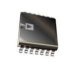
| 描述 | IC DGTL POT 1024POS 100K 14TSSOP数字电位计 IC 1024-pos 1% w/SPI interface |
| 产品分类 | |
| 品牌 | Analog Devices Inc |
| 产品手册 | |
| 产品图片 |
|
| rohs | 符合RoHS无铅 / 符合限制有害物质指令(RoHS)规范要求 |
| 产品系列 | 数字电位计 IC,Analog Devices AD5293BRUZ-100- |
| 数据手册 | |
| 产品型号 | AD5293BRUZ-100 |
| POT数量 | Single |
| 产品目录页面 | |
| 产品种类 | 数字电位计 IC |
| 供应商器件封装 | 14-TSSOP |
| 其它名称 | AD5293BRUZ100 |
| 包装 | 管件 |
| 商标 | Analog Devices |
| 存储器类型 | 易失 |
| 安装类型 | 表面贴装 |
| 安装风格 | SMD/SMT |
| 容差 | 1 % |
| 封装 | Tube |
| 封装/外壳 | 14-TSSOP(0.173",4.40mm 宽) |
| 封装/箱体 | TSSOP-14 |
| 工作温度 | -40°C ~ 105°C |
| 工作电源电压 | 5.5 V |
| 工厂包装数量 | 96 |
| 弧刷存储器 | Volatile |
| 抽头 | 1024 |
| 接口 | 4 线串行 |
| 数字接口 | SPI |
| 最大工作温度 | + 105 C |
| 最小工作温度 | - 40 C |
| 标准包装 | 96 |
| 每POT分接头 | 1024 |
| 温度系数 | 标准值 35 ppm/°C |
| 电压-电源 | 9 V ~ 33 V, ±9 V ~ 16.5 V |
| 电源电压-最大 | 33 V |
| 电源电压-最小 | 9 V |
| 电源电流 | 0.2 uA |
| 电路数 | 1 |
| 电阻 | 100 kOhms |
| 电阻(Ω) | 100k |
| 系列 | AD5293 |


- 商务部:美国ITC正式对集成电路等产品启动337调查
- 曝三星4nm工艺存在良率问题 高通将骁龙8 Gen1或转产台积电
- 太阳诱电将投资9.5亿元在常州建新厂生产MLCC 预计2023年完工
- 英特尔发布欧洲新工厂建设计划 深化IDM 2.0 战略
- 台积电先进制程称霸业界 有大客户加持明年业绩稳了
- 达到5530亿美元!SIA预计今年全球半导体销售额将创下新高
- 英特尔拟将自动驾驶子公司Mobileye上市 估值或超500亿美元
- 三星加码芯片和SET,合并消费电子和移动部门,撤换高东真等 CEO
- 三星电子宣布重大人事变动 还合并消费电子和移动部门
- 海关总署:前11个月进口集成电路产品价值2.52万亿元 增长14.8%


PDF Datasheet 数据手册内容提取
Single-Channel, 1024-Position, 1% R-Tolerance Digital Potentiometer Data Sheet AD5293 FEATURES FUNCTIONAL BLOCK DIAGRAM Single-channel, 1024-position resolution VDD RESET 20 kΩ, 50 kΩ, and 100 kΩ nominal resistance POWER-ON Calibrated 1% nominal resistor tolerance (resistor RESET AD5293 performance mode) Rheostat mode temperature coefficient: 35 ppm/°C VLOGIC Voltage divider temperature coefficient: 5 ppm/°C RDAC Single-supply operation: 9 V to 33 V SCLK 10 REGISTER A SERIAL Dual-supply operation: ±9 V to ±16.5 V SYNC INTERFACE W SPI-compatible serial interface Wiper setting readback DIN B SDO APPLICATIONS RDY MInestcrhuamneicnatla ptiootne:n gtiaoimn aentedr oreffpsleatc aedmjuesnttm ent VSS EXT_CAP GND 07675-001 Programmable voltage-to-current conversion Figure 1. Programmable filters, delays, and time constants Programmable power supply Low resolution DAC replacements Sensor calibration GENERAL DESCRIPTION The AD5293 is a single-channel, 1024-position digital potentiome- The AD5293 offers guaranteed industry-leading low resistor ter (in this data sheet, the terms digital potentiometer and RDAC tolerance errors of ±1% with a nominal temperature coefficient are used interchangeably) with a <1% end-to-end resistor tolerance of 35 ppm/°C. The low resistor tolerance feature simplifies open- error. The AD5293 performs the same electronic adjustment loop applications as well as precision calibration and tolerance function as a mechanical potentiometer with enhanced resolution, matching applications. solid state reliability, and superior low temperature coefficient The AD5293 is available in a compact 14-lead TSSOP package. performance. This device is capable of operating at high voltages The part is guaranteed to operate over the extended industrial and supporting both dual-supply operation at ±10.5 V to ±15 V temperature range of −40°C to +105°C. and single-supply operation at 21 V to 30 V. Rev. E Document Feedback Information furnished by Analog Devices is believed to be accurate and reliable. However, no responsibility is assumed by Analog Devices for its use, nor for any infringements of patents or other One Technology Way, P.O. Box 9106, Norwood, MA 02062-9106, U.S.A. rights of third parties that may result from its use. Specifications subject to change without notice. No license is granted by implication or otherwise under any patent or patent rights of Analog Devices. Tel: 781.329.4700 ©2009–2016 Analog Devices, Inc. All rights reserved. Trademarks and registered trademarks are the property of their respective owners. Technical Support www.analog.com
AD5293 Data Sheet TABLE OF CONTENTS Features ...............................................................................................1 RDAC Register ............................................................................ 18 Applications ........................................................................................1 Write Protection ......................................................................... 18 Functional Block Diagram ...............................................................1 Basic Operation .......................................................................... 18 General Description ..........................................................................1 Shutdown Mode .......................................................................... 18 Revision History ................................................................................2 Reset ............................................................................................. 19 Specifications ......................................................................................3 Resistor Performance Mode ...................................................... 19 Electrical Characteristics—20 kΩ Versions ...............................3 SDO Pin and Daisy-Chain Operation ..................................... 19 Resistor Performance Mode Code Range—20 kΩ Versions ...4 RDAC Architecture .................................................................... 20 Electrical Characteristics—50 kΩ and 100 kΩ Versions ..........5 Programming the Variable Resistor ......................................... 20 Resistor Performance Mode Code Range—50 kΩ and 100 kΩ Programming the Potentiometer Divider ............................... 21 Versions ...........................................................................................6 EXT_CAP Capacitor .................................................................. 21 Interface Timing Specifications ...................................................7 Terminal Voltage Operating Range .......................................... 21 Timing Diagrams ...........................................................................8 Applications Information .............................................................. 22 Absolute Maximum Ratings .............................................................9 High Voltage DAC ...................................................................... 22 Thermal Resistance .......................................................................9 Programmable Voltage Source with Boosted Output............ 22 ESD Caution ...................................................................................9 High Accuracy DAC .................................................................. 22 Pin Configuration and Function Descriptions ........................... 10 Variable Gain Instrumentation Amplifier ............................... 22 Typical Performance Characteristics ........................................... 11 Audio Volume Control .............................................................. 23 Test Circuits ..................................................................................... 17 Outline Dimensions ....................................................................... 24 Theory of Operation ...................................................................... 18 Ordering Guide ........................................................................... 24 Serial Data Interface ................................................................... 18 Shift Register ............................................................................... 18 REVISION HISTORY 3/16—Rev. D to Rev. E Added 50 kΩ and 100 kΩ Specifications ......................... Universal Changes to Figure 21 Caption and Figure 22 Caption .............. 13 Changes to Features Section............................................................ 1 Changes to Table 1 ............................................................................ 3 3/11—Rev. C to Rev. D Changes to Table 2 ............................................................................ 4 Changes to Table 1, Endnote 2 ................................................................ 4 Added Table 3; Renumbered Sequentially .................................... 5 Changes to Table 3, Endnote 2 ........................................................ 6 Added Table 4 .................................................................................... 6 Changes to Table 5 ............................................................................ 7 9/10—Rev. B to Rev. C Changes to Table 6 and Note 1, Table 7 ......................................... 9 Added CPOL = 0, CPHA = 1 to Figure 3 and Figure 4 Captions ..... 8 Changes to Typical Performance Characteristics Section ......... 11 Changes to SDO Pin and Daisy-Chain Operation Section ....... 19 Changes to Programming the Variable Resistor Section .......... 20 Changes to Programming the Potentiometer 3/10—Rev. A to Rev. B Divider Section ............................................................................... 21 Changes to Resistor Noise Density Conditions (Table 3) ........... 6 Changes to Ordering Guide Section ............................................ 24 12/09—Rev. 0 to Rev. A 4/09—Revision 0: Initial Version Rev. E | Page 2 of 24
Data Sheet AD5293 SPECIFICATIONS ELECTRICAL CHARACTERISTICS—20 kΩ VERSIONS V = 21 V to 33 V, V = 0 V; V = 10.5 V to 16.5 V, V = −10.5 V to −16.5 V; V = 2.7 V to 5.5 V, V = V , V = V , DD SS DD SS LOGIC A DD B SS −40°C < T < +105°C, unless otherwise noted. A Table 1. Parameter Symbol Conditions Min Typ1 Max Unit DC CHARACTERISTICS, RHEOSTAT MODE Resolution N 10 Bits Resistor Differential Nonlinearity2 R-DNL R −1 +1 LSB WB Resistor Integral Nonlinearity2 R-INL |V − V | = 26 V to 33 V −2 +2 LSB DD SS R-INL |V − V | = 21 V to 26 V −3 +3 LSB DD SS Nominal Resistor Tolerance ∆R /R See Table 2 −1 ±0.5 +1 % AB AB (R-Perf Mode)3 Nominal Resistor Tolerance ∆R /R ±7 % AB AB (Normal Mode) Resistance Temperature Coefficient4 (∆R /R )/∆T × 106 35 ppm/°C AB AB Wiper Resistance R 60 100 Ω W DC CHARACTERISTICS, POTENTIOMETER DIVIDER MODE Resolution N 10 Bits Differential Nonlinearity5 DNL −1 +1 LSB Integral Nonlinearity5 INL −1.5 +1.5 LSB Voltage Divider Temperature (∆V /V )/∆T × 106 Code = half scale 5 ppm/°C W W Coefficient4 Full-Scale Error V Code = full scale −8 0 LSB WFSE Zero-Scale Error V Code = zero scale 0 8 LSB WZSE RESISTOR TERMINALS Terminal Voltage Range6 V , V , V V V V A B W SS DD Capacitance A, Capacitance B4 C , C f = 1 MHz, measured to GND, 85 pF A B code = half-scale Capacitance W4 C f = 1 MHz, measured to GND, 65 pF W code = half-scale Common-Mode Leakage Current I V = V = V ±1 nA CM A B W DIGITAL INPUTS JEDEC compliant Input Logic High V V = 2.7 V to 5.5 V 2.0 V IH LOGIC Input Logic Low V V = 2.7 V to 5.5 V 0.8 V IL LOGIC Input Current I V = 0 V or V ±1 µA IL IN LOGIC Input Capacitance4 C 5 pF IL DIGITAL OUTPUTS (SDO and RDY) Output High Voltage V R = 2.2 kΩ to V V − 0.4 V OH PULL_UP LOGIC LOGIC Output Low Voltage V R = 2.2 kΩ to V GND + 0.4 V OL PULL_UP LOGIC Tristate Leakage Current −1 +1 µA Output Capacitance4 C 5 pF OL POWER SUPPLIES Single-Supply Power Range V V = 0 V 9 33 V DD SS Dual-Supply Power Range V /V ±9 ±16.5 V DD SS Positive Supply Current I V /V = ±16.5 V 0.1 2 µA DD DD SS Negative Supply Current I V /V = ±16.5 V −2 −0.1 µA SS DD SS Logic Supply Range V 2.7 5.5 V LOGIC Logic Supply Current I V = 5 V; V = 5 V or V = GND 1 10 µA LOGIC LOGIC IH IL Power Dissipation7 P V = 5 V or V = GND 8 110 µW DISS IH IL Power Supply Rejection Ratio4 PSSR ∆V /∆V = ±15 V ± 10% 0.103 %/% DD SS Rev. E | Page 3 of 24
AD5293 Data Sheet Parameter Symbol Conditions Min Typ1 Max Unit DYNAMIC CHARACTERISTICS4, 8 Bandwidth BW −3 dB 520 kHz Total Harmonic Distortion THD V = 1 V rms, V = 0 V, f = 1 kHz, −93 dB W A B V Settling Time t V = 30 V, V = 0 V, ±0.5 LSB error W S A B band, initial code = zero scale Code = full scale, R-normal mode 750 ns Code = full scale, R-perf mode 2.5 µs Code = half scale, R-normal mode 2.5 µs Code = half scale, R-perf mode 5 µs Resistor Noise Density e R = 10 kΩ, T = 25°C, 10 nV/√Hz N_WB WB A 0 kHz to 200 kHz 1 Typicals represent average readings at 25°C; VDD = +15 V, VSS = −15 V, and VLOGIC = 5 V. 2 Resistor position nonlinearity error. R-INL is the deviation from an ideal value measured between RWB at Code 0x00B to Code 0x3FF or between RWA at Code 0x3F3 to Code 0x000. R-DNL measures the relative step change from ideal between successive tap positions. The specification is guaranteed in resistor performance mode with a wiper current of 1 mA for VA < 12 V and 1.2 mA for VA ≥ 12 V. 3 The terms resistor performance mode and R-perf mode are used interchangeably. 4 Guaranteed by design; not subject to production test. 5 INL and DNL are measured at VW with the RDAC configured as a potentiometer divider similar to a voltage output DAC. VA = VDD and VB = 0 V. DNL specification limits of ±1 LSB maximum are guaranteed monotonic operating conditions. 6 The A, B, and W resistor terminals have no limitations on polarity with respect to each other. Dual-supply operation enables ground-referenced bipolar signal adjustment. 7 PDISS is calculated from (IDD × VDD) + (ISS × VSS) + (ILOGIC × VLOGIC). 8 All dynamic characteristics use VDD = +15 V, VSS = −15 V, and VLOGIC = 5 V. RESISTOR PERFORMANCE MODE CODE RANGE—20 kΩ VERSIONS Table 2. R = 20 kΩ Resistor AB Tolerance |VDD − VSS| = 30 V to 33 V |VDD − VSS| = 26 V to 30 V |VDD − VSS| = 22 V to 26 V |VDD − VSS| = 21 V to 22 V per Code R R R R R R R R WB WA WB WA WB WA WB WA 1% R-Tolerance From 0x15E From 0x000 From 0x1F4 From 0x000 From 0x1F4 From 0x000 N/A N/A to 0x3FF to 0x2A1 to 0x3FF to 0x20B to 0x3FF to 0x20B 2% R-Tolerance From 0x8C From 0x000 From 0xB4 From 0x000 From 0xFA From 0x000 From 0xFA From 0x000 to 0x3FF to 0x373 to 0x3FF to 0x34B to 0x3FF to 0x305 to 0x3FF to 0x305 3% R-Tolerance From 0x5A From 0x000 From 0x64 From 0x000 From 0x78 From 0x000 From 0x78 From 0x000 to 0x3FF to 0x3A5 to 0x3FF to 0x39B to 0x3FF to 0x387 to 0x3FF to 0x387 Rev. E | Page 4 of 24
Data Sheet AD5293 ELECTRICAL CHARACTERISTICS—50 kΩ AND 100 kΩ VERSIONS V = 21 V to 33 V, V = 0 V; V = 10.5 V to 16.5 V, V = −10.5 V to −16.5 V; V = 2.7 V to 5.5 V, V = V , V = V , DD SS DD SS LOGIC A DD B SS −40°C < T < +105°C, unless otherwise noted. A Table 3. Parameter Symbol Conditions Min Typ1 Max Unit DC CHARACTERISTICS, RHEOSTAT MODE Resolution N 10 Bits Resistor Differential Nonlinearity2 R-DNL R −1 +1 LSB WB Resistor Integral Nonlinearity2 R-INL −2 +2 LSB Nominal Resistor Tolerance ∆R /R See Table 4 −1 ±0.5 +1 % AB AB (R-Perf Mode)3 Nominal Resistor Tolerance ∆R /R ±20 % AB AB (Normal Mode) Resistance Temperature Coefficient4 (∆R /R )/∆T × 106 35 ppm/°C AB AB Wiper Resistance R 60 100 Ω W DC CHARACTERISTICS, POTENTIOMETER DIVIDER MODE Resolution N 10 Bits Differential Nonlinearity5 DNL −1 +1 LSB Integral Nonlinearity5 INL −1.5 +1.5 LSB Voltage Divider Temperature (∆V /V )/∆T × 106 Code = half scale 5 ppm/°C W W Coefficient4 Full-Scale Error V Code = full scale −8 +1 LSB WFSE Zero-Scale Error V Code = zero scale 0 8 LSB WZSE RESISTOR TERMINALS Terminal Voltage Range6 V , V , V V V V A B W SS DD Capacitance A, Capacitance B4 C , C f = 1 MHz, measured to GND, 85 pF A B code = half-scale Capacitance W4 C f = 1 MHz, measured to GND, 65 pF W code = half-scale Common-Mode Leakage Current I V = V = V ±1 nA CM A B W DIGITAL INPUTS JEDEC compliant Input Logic High V V = 2.7 V to 5.5 V 2.0 V IH LOGIC Input Logic Low V V = 2.7 V to 5.5 V 0.8 V IL LOGIC Input Current I V = 0 V or V ±1 µA IL IN LOGIC Input Capacitance4 C 5 pF IL DIGITAL OUTPUTS (SDO and RDY) Output High Voltage V R = 2.2 kΩ to V V − 0.4 V OH PULL_UP LOGIC LOGIC Output Low Voltage V R = 2.2 kΩ to V GND + 0.4 V OL PULL_UP LOGIC Tristate Leakage Current −1 +1 µA Output Capacitance4 C 5 pF OL POWER SUPPLIES Single-Supply Power Range V V = 0 V 9 33 V DD SS Dual-Supply Power Range V /V ±9 ±16.5 V DD SS Positive Supply Current I V /V = ±16.5 V 0.1 2 µA DD DD SS Negative Supply Current I V /V = ±16.5 V −2 −0.1 µA SS DD SS Logic Supply Range V 2.7 5.5 V LOGIC Logic Supply Current I V = 5 V; V = 5 V or V = GND 1 10 µA LOGIC LOGIC IH IL Power Dissipation7 P V = 5 V or V = GND 8 110 µW DISS IH IL Power Supply Rejection Ratio4 PSSR ∆V /∆V = ±15 V ± 10% DD SS R = 50 kΩ 0.039 %/% AB R = 100 kΩ 0.021 %/% AB Rev. E | Page 5 of 24
AD5293 Data Sheet Parameter Symbol Conditions Min Typ1 Max Unit DYNAMIC CHARACTERISTICS4, 8 Bandwidth BW −3 dB kHz RAB = 50 kΩ 210 R = 100 kΩ 105 AB Total Harmonic Distortion THD V = 1 V rms, V = 0 V, f = 1 kHz W A B R = 50 kΩ −101 dB AB R = 100 kΩ −106 dB AB V Settling Time t V = 30 V, V = 0 V, ±0.5 LSB error W S A B band, initial code = zero scale Code = full scale, R-normal mode 750 ns Code = full scale, R-perf mode 2.5 µs Code = half scale, R-normal mode, 7 µs R = 50 kΩ AB Code = half scale, R-normal mode, 14 µs R = 100 kΩ AB Code = half scale, R-perf mode, 9 µs R = 50 kΩ AB Code = half scale, R-perf mode, 16 µs R = 100 kΩ AB Resistor Noise Density e Code = half scale, T = 25°C, N_WB A 0 kHz to 200 kHz, R = 50 kΩ 18 nV/√Hz AB R = 100 kΩ 27 nV/√Hz AB 1 Typicals represent average readings at 25°C; VDD = +15 V, VSS = −15 V, and VLOGIC = 5 V. 2 Resistor position nonlinearity error. R-INL is the deviation from an ideal value measured between RWB at Code 0x00B to Code 0x3FF or between RWA at Code 0x3F3 to Code 0x000. R-DNL measures the relative step change from ideal between successive tap positions. The specification is guaranteed in resistor performance mode with a wiper current of 1 mA for VA < 12 V and 1.2 mA for VA ≥ 12 V. 3 The terms resistor performance mode and R-perf mode are used interchangeably. 4 Guaranteed by design; not subject to production test. 5 INL and DNL are measured at VW with the RDAC configured as a potentiometer divider similar to a voltage output DAC. VA = VDD and VB = 0 V. DNL specification limits of ±1 LSB maximum are guaranteed monotonic operating conditions. 6 The A, B, and W resistor terminals have no limitations on polarity with respect to each other. Dual-supply operation enables ground-referenced bipolar signal adjustment. 7 PDISS is calculated from (IDD × VDD) + (ISS × VSS) + (ILOGIC × VLOGIC). 8 All dynamic characteristics use VDD = +15 V, VSS = −15 V, and VLOGIC = 5 V. RESISTOR PERFORMANCE MODE CODE RANGE—50 kΩ AND 100 kΩ VERSIONS Table 4. R = 50 kΩ R = 100 kΩ AB AB Resistor Tolerance |VDD − VSS| = 26 V to 33 V |VDD − VSS| = 21 V to 26 V |VDD − VSS| = 26 V to 33 V |VDD − VSS| = 21 V to 26 V per Code R R R R R R R R WB WA WB WA WB WA WB WA 1% R-Tolerance From 0x08C From 0x000 From 0x0B4 From 0x000 From 0x04B From 0x000 From 0x064 From 0x000 to 0x3FF to 0x35F to 0x3FF to 0x31E to 0x3FF to 0x3B4 to 0x3FF to 0x39B 2% R-Tolerance From 0X03C From 0x000 From 0x050 From 0x000 From 0x028 From 0x000 From 0x028 From 0x000 to 0x3FF to 0x3C3 to 0x3FF to 0x3AF to 0x3FF to 0x3D7 to 0x3FF to 0x3D7 3% R-Tolerance From 0X028 From 0x000 From 0x032 From 0x000 From 0x019 From 0x000 From 0x019 From 0x000 to 0x3FF to 0x3D7 to 0x3FF to 0x3CD to 0x3FF to 0x3E6 to 0x3FF to 0x3E6 Rev. E | Page 6 of 24
Data Sheet AD5293 INTERFACE TIMING SPECIFICATIONS V = V = ±15 V, V = 2.7 V to 5.5 V, and −40°C < T < +105°C. All specifications T to T , unless otherwise noted. DD SS LOGIC A MIN MAX Table 5. Parameter Limit1 Unit Test Conditions/Comments t2 20 ns min SCLK cycle time 1 t 10 ns min SCLK high time 2 t 10 ns min SCLK low time 3 t 10 ns min SYNC to SCLK falling edge setup time 4 t 5 ns min Data setup time 5 t 5 ns min Data hold time 6 t 1 ns min SCLK falling edge to SYNC rising edge 7 t 4003 ns min Minimum SYNC high time 8 t 14 ns min SYNC rising edge to next SCLK fall ignored 9 t 4 1 ns min RDY rise to SYNC falling edge 10 t 4 40 ns max SYNC rise to RDY fall time 11 t 4 2.4 µs max RDY low time, RDAC register write command execute time (resistor performance mode) 12 t 4 410 ns max RDY low time, RDAC register write command execute time (normal mode) 12 t 4 1.5 ms max Software\hardware reset 12 t 4 450 ns max RDY low time, RDAC register read command execute time 13 t 4 450 ns max SCLK rising edge to SDO valid 14 t 20 ns min Minimum RESET pulse width (asynchronous) RESET tPOWER-UP5 2 ms max Power-on time to half scale 1 All input signals are specified with tR = tF = 1 ns/V (10% to 90% of VDD) and timed from a voltage level of (VIL + VIH)/2. 2 Maximum SCLK frequency = 50 MHz. 3 Refer to t12 and t13 for RDAC register commands operations. 4 RPULL_UP = 2.2 kΩ to VLOGIC with a capacitance load of 168 pF. 5 Typical power supply voltage slew-rate of 2 V/ms. DB9 (MSB) DB0 (LSB) 0 0 C3 C2 C1 C0 D9 D8 D7 D6 D5 D4 D3 D2 D1 D0 CONTROL BITS DATA BITS 07675-002 Figure 2. Shift Register Contents Rev. E | Page 7 of 24
AD5293 Data Sheet TIMING DIAGRAMS t4 t2 t1 t7 SCLK t8 t3 t9 SYNC t5 t6 DIN X X C3 C2 D7 D6 D2 D1 D0 SDO t10 t11 t12 RDY RESET tRESET 07675-003 Figure 3. Write Timing Diagram, CPOL = 0, CPHA =1 SCLK t9 SYNC DIN X X C3 D0 D0 X X C3 D1 D0 t14 SDO X X C3 D1 D0 RDY t11 t13 07675-004 Figure 4. Read Timing Diagram, CPOL = 0, CPHA =1 Rev. E | Page 8 of 24
Data Sheet AD5293 ABSOLUTE MAXIMUM RATINGS T = 25°C, unless otherwise noted. A Stresses at or above those listed under Absolute Maximum Ratings may cause permanent damage to the product. This is a Table 6. stress rating only; functional operation of the product at these Parameter Rating or any other conditions above those indicated in the operational V to GND −0.3 V to +35 V DD section of this specification is not implied. Operation beyond V to GND +0.3 V to −25 V SS the maximum operating conditions for extended periods may V to GND −0.3 V to +7 V LOGIC affect product reliability. V to V 35 V DD SS V , V , V to GND V − 0.3 V, V + 0.3 V THERMAL RESISTANCE A B W SS DD Digital Input and Output Voltage to GND −0.3 V to V +0.3 V LOGIC θ is specified for the worst-case conditions, that is, a device JA EXT_CAP Voltage to GND −0.3 V to +7 V soldered in a circuit board for surface-mount packages. I , I , I A B W Continuous Table 7. Thermal Resistance RAB = 20 kΩ ±3 mA Package Type θJA θJC Unit R = 50 kΩ, 100 kΩ ±2 mA 14-Lead TSSOP 931 20 °C/W AB Pulsed1 1 JEDEC 2S2P test board, still air (from 0 m/sec to 1 m/sec of air flow). Frequency > 10 kHz MCC2/d3 Frequency ≤ 10 kHz MCC2/√d3 Operating Temperature Range −40°C to +105°C ESD CAUTION Maximum Junction Temperature (T max) 150°C J Storage Temperature Range −65°C to +150°C Reflow Soldering Peak Temperature 260°C Time at Peak Temperature 20 sec to 40 sec Package Power Dissipation (T max − T )/θ J A JA 1 Maximum terminal current is bounded by the maximum current handling of the switches, maximum power dissipation of the package, and maximum applied voltage across any two of the A, B, and W terminals at a given resistance. 2 Maximum continuous current. 3 Pulse duty factor. Rev. E | Page 9 of 24
AD5293 Data Sheet PIN CONFIGURATION AND FUNCTION DESCRIPTIONS RESET 1 14 RDY VSS 2 13 SDO A 3 AD5293 12 SYNC W 4 TOP VIEW 11 SCLK B 5 Not to Scale 10 DIN EXT_CVADPD 67 98 GVLNODGIC 07675-005 Figure 5. Pin Configuration Table 8. Pin Function Descriptions Pin No. Mnemonic Description 1 RESET Hardware Reset Pin. Sets the RDAC register to midscale. RESET is activated at the logic high transition. Tie RESET to V if not used. LOGIC 2 V Negative Supply. Connect to 0 V for single-supply applications. This pin should be decoupled with 0.1 µF ceramic SS capacitors and 10 µF capacitors. 3 A Terminal A of RDAC. V ≤ V ≤ V . SS A DD 4 W Wiper Terminal W of RDAC. V ≤ V ≤ V . SS W DD 5 B Terminal B of RDAC. V ≤ V ≤ V . SS B DD 6 V Positive Power Supply. This pin should be decoupled with 0.1 µF ceramic capacitors and 10 µF capacitors. DD 7 EXT_CAP Connect a 1 µF capacitor to EXT_CAP. This capacitor must have a voltage rating of ≥7 V. 8 V Logic Power Supply, 2.7 V to 5.5 V. This pin should be decoupled with 0.1 µF ceramic capacitors and 10 µF capacitors. LOGIC 9 GND Ground Pin, Logic Ground Reference. 10 DIN Serial Data Input. This part has a 16-bit shift register. Data is clocked into the register on the falling edge of the serial clock input. 11 SCLK Serial Clock Input. Data is clocked into the shift register on the falling edge of the serial clock input. Data can be transferred at rates up to 50 MHz. 12 SYNC Falling Edge Synchronization Signal. This is the frame synchronization signal for the input data. When SYNC goes low, it enables the shift register, and data is transferred in on the falling edges of the following clocks. The selected register is updated on the rising edge of SYNC, following the 16th clock cycle. If SYNC is taken high before the 16th clock cycle, the rising edge of SYNC acts as an interrupt, and the write sequence is ignored by the DAC. 13 SDO Serial Data Output. This open-drain output requires an external pull-up resistor. SDO can be used to clock data from the serial register in daisy-chain mode or in readback mode. 14 RDY Ready Pin. This active-high, open-drain output identifies the completion of a write or read operation to or from the RDAC register. Rev. E | Page 10 of 24
Data Sheet AD5293 TYPICAL PERFORMANCE CHARACTERISTICS 1.0 1.0 –40°C 20kΩ TEMPERATURE = 25°C 0.8 +25°C 0.8 50kΩ 100kΩ +105°C 0.6 0.6 0.4 0.4 B) 0.2 B) 0.2 S S L (L 0 L (L 0 N N I –0.2 I –0.2 –0.4 –0.4 –0.6 –0.6 –0.8 –0.8 RAB = 20kΩ –1.00 128 256 38C4ODE 5(D12ecima6l4)0 768 896 1023 07675-106 –1.00 128 256 38C4ODE 5(D12ecima6l4)0 768 896 1023 07675-215 Figure 6. R-INL in R-Perf Mode vs. Code vs. Temperature Figure 9. R-INL in R-Perf Mode vs. Code vs. Nominal Resistance 0.6 0.6 RAB = 20kΩ TEMPERATURE = 25°C 0.5 0.5 0.4 0.4 0.3 0.3 B) B) S 0.2 S 0.2 L L L ( L ( N 0.1 N 0.1 D D 0 0 –0.1 –0.1 –0.2 –0.2 20kΩ 50kΩ –40°C +25°C +105°C 100kΩ –0.30 128 256 38C4ODE 5(D12ecima6l4)0 768 896 1023 07675-007 –0.30 128 256 38C4ODE 5(D12ecima6l4)0 768 896 1023 07675-211 Figure 7. R-DNL in R-Perf Mode vs. Code vs. Temperature Figure 10. R-DNL in R-Perf Mode vs. Code vs. Nominal Resistance 1.0 1.0 RAB = 20kΩ 2500kkΩΩ TEMPERATURE = 25°C 0.8 0.8 100kΩ 0.6 0.6 0.4 0.4 B) B) S S NL (L 0.2 NL (L 0.2 I I 0 0 –0.2 –0.2 –0.4 –0.4 –40°C +25°C +105°C –0.60 128 256 38C4ODE 5(D12ecima6l4)0 768 896 1023 07675-010 –0.60 128 256 38C4ODE 5(D12ecima6l4)0 768 896 1023 07675-216 Figure 8. R-INL in Normal Mode vs. Code vs. Temperature Figure 11. R-INL in Normal Mode vs. Code vs. Nominal Resistance Rev. E | Page 11 of 24
AD5293 Data Sheet 0.15 0.15 RAB = 20kΩ 20kΩ TEMPERATURE = 25°C 50kΩ 100kΩ 0.10 0.10 0.05 0.05 B) 0 B) 0 S S L L L ( L ( DN–0.05 DN–0.05 –0.10 –0.10 –0.15 –0.15 –40°C +25°C +105°C –0.200 128 256 38C4ODE 5(D12ecima6l4)0 768 896 1023 07675-011 –0.200 128 256 38C4ODE 5(D12ecima6l4)0 768 896 1023 07675-213 Figure 12. R-DNL in Normal Mode vs. Code vs. Temperature Figure 15. R-DNL in Normal Mode vs. Code vs. Nominal Resistance 1.5 0.8 RAB = 20kΩ TEMPERATURE = 25°C 1.0 0.6 0.5 0.2 B) B) S S NL (L 0 NL (L 0 I I –0.5 –0.2 –1.0 –0.6 20kΩ 50kΩ –40°C +25°C +105°C 100kΩ –1.50 128 256 38C4ODE 5(D12ecima6l4)0 768 896 1023 07675-014 –0.80 128 256 38C4ODE 5(D12ecima6l4)0 768 896 1023 07675-207 Figure 13. INL in R-Perf Mode vs. Code vs. Temperature Figure 16. INL in R-Perf Mode vs. Code vs. Nominal Resistance 0.6 0.6 RAB = 20kΩ TEMPERATURE = 25°C 0.5 0.5 0.4 0.4 0.3 0.3 B) L (LS 0.2 LSB) 0.2 DN L ( 0.1 N 0.1 D 0 0 –0.1 –0.1 –0.20 128 256–40°C38C4ODE 5(D1+2e2c5i°mCa6l4)0 7+61805°C896 1023 07675-015 ––00..320 251000kk01ΩkΩ2Ω8 256 38C4ODE 5(D12ecima6l4)0 768 896 1023 07675-203 Figure 14. DNL in R-Perf Mode vs. Code vs. Temperature Figure 17. DNL in R-Perf Mode vs. Code vs. Nominal Resistance Rev. E | Page 12 of 24
Data Sheet AD5293 0.8 0.8 RAB = 20kΩ +–4205°°CC 2500kkΩΩ TEMPERATURE = 25°C 0.6 0.6 100kΩ +105°C 0.4 0.4 0.2 0.2 B) B) S S L (L 0 L (L 0 N N I I –0.2 –0.2 –0.4 –0.4 –0.6 –0.6 –0.80 128 256 38C4ODE 5(D12ecima6l4)0 768 896 1023 07675-018 –0.80 128 256 38C4ODE 5(D12ecima6l4)0 768 896 1023 07675-209 Figure 18. INL in Normal Mode vs. Code vs. Temperature Figure 21. INL in Normal Mode vs. Code vs. Nominal Resistance 0.10 0.08 –40°C 20kΩ +25°C 50kΩ 100kΩ 0.05 +105°C 0.04 0 0 B) B) S S L (L–0.05 L (L–0.04 N N D D –0.10 –0.08 –0.15 –0.12 RAB = 20kΩ TEMPERATURE = 25°C –0.200 128 256 38C4ODE 5(D12ecima6l4)0 768 896 1023 07675-019 –0.160 128 256 38C4ODE 5(D12ecima6l4)0 768 896 1023 07675-205 Figure 19. DNL in Normal Mode vs. Code vs. Temperature Figure 22. DNL in Normal Mode vs. Code vs. Nominal Resistance 450 0.20 400 VVDLODG/VICS S= =+ 5±V15V 0.18 VDD = ±15V 350 A) 0.16 T (nA) 300 ILOGIC (mOGIC 0.14 LY CURREN 221505000 CURRENT IL 00..001.821 SUPP 100 IDD UPPLY 0.06 50 S 0.04 0 0.02 ISS –50–40–30–20–10 0 1T0EM2P0ER3A0TU4R0E 5(°0C)60 70 80 90 100 07675-022 00 0.5 1.0 D1I.G5ITA2L. 0INPU2T.5 VOL3T.0AGE3 (.V5) 4.0 4.5 5.0 07675-057 Figure 20. Supply Current vs. Temperature Figure 23. Supply Current, ILOGIC, vs. Digital Input Voltage. Rev. E | Page 13 of 24
AD5293 Data Sheet 700 700 C) 600 VVDSSD= = 02 3V00kVΩ, m/°C) 600 VVDSSD= = 0 23V00kVΩ O (ppm/° 500 15000kkΩΩ PCO (pp 500 5100k0ΩkΩ C M P E EM 400 E T 400 T D E O D M MO 300 ER 300 AT ET ST 200 OM 200 RHEO 100 TENTI 100 O P 00 256 CODE 5(D12ecimal) 768 1023 07675-023 00 256 CODE 5(D12ecimal) 768 1023 07675-024 Figure 24. Rheostat Mode Tempco ΔRWB/ΔT vs. Code Figure 27. Potentiometer Mode Tempco ΔRWB/ΔT vs. Code 0 0 0x200 –5 0x200 –10 0x100 –10 0x100 0x080 –15 –20 0x040 0x080 dB) –20 0x040 dB) –30 0x020 N ( –25 N ( 0x010 GAI –30 0x020 GAI –40 0x008 0x010 0x004 –35 –50 0x008 0x002 –40 –60 0x001 –45 0x004 0x002 0x001 –5010 100 FR1kEQUENCY 1(0Hkz) 100k 1M 07675-025 –7010 100 FR1kEQUENCY 1(H0kz) 100k 1M 07675-201 Figure 25. 20 kΩ Gain vs. Frequency vs. Code Figure 28. 100 kΩ Gain vs. Frequency vs. Code 0 0 100kΩ 0x200 20kΩ 50kΩ –10 0x100 –10 0x080 –20 –20 0x040 B) B)–30 N (d –30 0x020 R (d GAI 0x010 SR–40 P –40 0x008 –50 0x004 –50 –60 0x002 0x001 –6010 100 FR1kEQUENCY 1(H0kz) 100k 1M 07674-200 –70100 1k FREQU1E0NkCY (Hz) 100k 1M 07675-026 Figure 26. 50 kΩ Gain vs. Frequency vs. Code Figure 29. Power Supply Rejection Ratio (PSRR) vs. Frequency Rev. E | Page 14 of 24
Data Sheet AD5293 0 0 VDD/VSS = ±15V VDD/VSS = ±15V, CODE = HALF SCALE CODE = HALF SCALE –15 VIN = 1V rms –20 fIN = 1kHz Noise BW = 22kHz NOISE BW = 22kHz 20kΩ 20kΩ –30 50kΩ –40 50kΩ 100kΩ 100kΩ B) –45 B) d d –60 N ( N ( + –60 + HD HD –80 T –75 T –100 –90 –120 –105 –120100 1k FREQUENC1Y0 (kHz) 100k 07675-027 –1400.001 0.01 AMPLITU0D.1E (V rms) 1 10 07675-220 Figure 30. Total Harmonic Distortion + Noise (THD + N) vs. Frequency Figure 33. Total Harmonic Distortion + Noise (THD + N) vs. Amplitude 1,000,000 8 900,000 22220000kkkk –––– 0712p555p00FppFFF 55110000kk00 kk–– ––12 550700p5pppFFFF 7 VVVDABD ==/ VVVSDSSSD = 30V/0V 800,000 50k – 0pF 100k – 150pF 50k – 75pF 100k – 250pF mA) 6 H (Hz)670000,,000000 (B_MAX 5 T W WID500,000 AL I 4 D C BAN400,000 RETI 3 20kΩ 300,000 O E 50kΩ H 2 200,000 T 100,000 1 100kΩ 00 8 16 CO3D2E (Deci6m4al) 128 256 512 07675-222 00 256 CODE 5(D12ecimal) 768 1023 07675-029 Figure 31. Maximum Bandwidth vs. Code vs. Net Capacitance Figure 34. Theoretical Maximum Current vs. Code 35 40 V W B , C O D E : FNUOLRLM SACLA MLEO,DE VDD/VSS=±15V 30 32 VA=VDD VDD/VSS = 30V/0V VB=VSS 25 VLOGIC = 5V 24 CODE=HALFCODE VA = VDD VB = VSS 16 LTAGE (V) 1250 V W B , C O D E : FRU-PLLE RSFC AMLOED,E GE (μV) 08 O A V 10 T L SYNC O –8 V 5 VWB, CODE: HALF-SCALE, 2500kkΩΩ –16 NORMAL MODE 100kΩ 0 VWB, CODE: HALF-SCALE, 2500kkΩΩ –24 R-PERF MODE 100kΩ –5–2 –1 0 1 2 3 4 5T6IME7 (µs8) 9 10 11 12 13 14 15 07675-058 ––4302 –0.5 0 5 10 15TIM2E0(µs)25 30 35 40 45 07675-221 Figure 32. Large Signal Settling Time, Code from Zero Scale to Full Scale Figure 35. Digital Feedthrough Rev. E | Page 15 of 24
AD5293 Data Sheet 80 1.2 20kΩ VA = VDD 1.0 VVDLODG/VICS S= =+ 5±V15V 70 5100k0ΩkΩ VTEB M=P VESRSATURE = 25°C 0.8 VVAB == VVDSSD 93) 60 2 20kΩ D5 E (V) 00..46 5100k0ΩkΩ ODES (A 4500 G C VOLTA 0.20 ER OF 30 B –0.2 UM 20 N –0.4 10 –0.6 –0.8–2 0 2 4 6TIME (µ8s) 10 12 14 16 07675-035 021 26VOLTAGE VDD/VSS30 33 07675-219 Figure 36. Maximum Transition Glitch Figure 38. Code Range > 1% R-Tolerance Error vs. Voltage 300 VDD/VSS= ±15V 20kΩ 250 50kΩ 93) 100kΩ 2 5 AD 200 S ( E D CO 150 F O R E 100 B M U N 50 0–40–30–20–10 0 1T0EM2P0ER3A0TU4R0E 5(°0C)60 70 80 90 100 07675-056 Figure 37. Code Range > 1% R-Tolerance Error vs. Temperature Rev. E | Page 16 of 24
Data Sheet AD5293 TEST CIRCUITS Figure 39 to Figure 44 define the test conditions used in the Specifications section. NC DUT A IW VA W V+ = VDD ± 10% B NC = NO CVOMNSNECT 07675-030 V+ ~ VDD BA W VMS PPSSSR R(% (d/%B)) == ΔΔ20VV MDloDSg%%ΔΔVVMDDS 07675-033 Figure 39. Resistor Position Nonlinearity Error Figure 42. Power Supply Sensitivity (PSS, PSRR) (Rheostat Operation: R-INL, R-DNL) A +15V DUT V+ = VDD W A 1LSB = V+/2N VIN DUT V+ W OFFSET B OP42 VOUT B GND VMS 07675-031 2.5V –15V 07675-036 Figure 40. Potentiometer Divider Nonlinearity Error (INL, DNL) Figure 43. Gain vs. Frequency +15V –15V NC GND 0.1V GND DUT RWB = IWB VDD A ICM B W CODE = 0x00+0R.1WV = RW2B DVUSSTGND B W +–1155VV IWB – GND A = NC VSS TO VDD 07675-032 NC+15V –15VGND NC = NO CONNECT 07675-037 Figure 41. Wiper Resistance Figure 44. Common-Mode Leakage Current Rev. E | Page 17 of 24
AD5293 Data Sheet THEORY OF OPERATION The AD5293 digital potentiometer is designed to operate as WRITE PROTECTION a true variable resistor for analog signals that remain within On power-up, the serial data input register write command for the terminal voltage range of V < V < V . The patented SS TERM DD the RDAC register is disabled. The RDAC write protect bit, C1 ±1% resistor tolerance feature helps to minimize the total RDAC of the control register (see Table 12 and Table 13), is set to 0 by resistance error, which reduces the overall system error by default. This disables any change of the RDAC register content, offering better absolute matching and improved open-loop regardless of the software commands, except that the RDAC register performance. The digital potentiometer wiper position is can be refreshed to midscale using the software reset command determined by the RDAC register contents. The RDAC register (Command 3, see Table 11) or through hardware, using the acts as a scratchpad register, allowing as many value changes RESET pin. To enable programming of the variable resistor wiper as necessary to place the potentiometer wiper in the correct position (programming the RDAC register), the write protect bit, position. The RDAC register can be programmed with any C1 of the control register, must first be programmed. This is position setting via the standard serial peripheral interface (SPI) accomplished by loading the serial data input register with by loading the 16-bit data-word. Command 4 (see Table 11). SERIAL DATA INTERFACE BASIC OPERATION The AD5293 contains a serial interface (SYNC, SCLK, DIN, and The basic mode of setting the variable resistor wiper position SDO) that is compatible with SPI standards, as well as most DSPs. (programming the RDAC register) is accomplished by loading the The device allows data to be written to every register via the SPI. serial data input register with Command 1 (see Table 11) and the SHIFT REGISTER desired wiper position data. The RDY pin can be used to monitor the completion of this RDAC register write command. Command 2 The AD5293 shift register is 16 bits wide (see Figure 2). The 16-bit can be used to read back the contents of the RDAC register (see data-word consists of two unused bits, which are set to 0, followed Table 11). After issuing the readback command, the RDY pin by four control bits and 10 RDAC data bits. Data is loaded MSB can be monitored to indicate when the data is available to be first (Bit 15). The four control bits determine the function of the read out on SDO in the next SPI operation. Instead of monitoring software command (see Table 11). Figure 3 shows a timing diagram the RDY pin, a minimum delay can be implemented when of a typical write sequence. executing a write or read command (see Table 5). Table 9 The write sequence begins by bringing the SYNC line low. The provides an example listing of a sequence of serial data input SYNC pin must be held low until the complete data-word is loaded (DIN) words with the serial data output appearing at the SDO from the DIN pin. When SYNC returns high, the serial data-word pin in hexadecimal format for an RDAC write and read. is decoded according to the instructions in Table 11. The Table 9. RDAC Register Write and Read command bits (Cx) control the operation of the digital potentiometer. The data bits (Dx) are the values that are loaded DIN SDO Action into the decoded register. The AD5293 has an internal counter 0x1802 0xXXXX1 Enable update of wiper position. that counts a multiple of 16 bits (per frame) for proper operation. 0x0500 0x1802 Write 0x100 to the RDAC register. Wiper moves to ¼ full-scale position. For example, the AD5293 works with a 32-bit word, but it cannot 0x0800 0x0500 Prepare data read from RDAC register. work properly with a 31- or 33-bit word. The AD5293 does not 0x0000 0x0100 NOP (Instruction 0) sends a 16-bit word require a continuous SCLK, when SYNC is high, and all interface out of SDO, where the last 10 bits contain pins should be operated close to the supply rails to minimize the contents of the RDAC register. power consumption in the digital input buffers. 1 X = unknown. RDAC REGISTER The RDAC register directly controls the position of the digital SHUTDOWN MODE potentiometer wiper. For example, when the RDAC register is The AD5293 can be placed in shutdown mode by executing the loaded with all zeros, the wiper is connected to Terminal B of the software shutdown command (see Command 6 in Table 11), and variable resistor. The RDAC register is a standard logic register; setting the LSB to 1. This feature places the RDAC in a special state there is no restriction on the number of changes allowed. The RDY in which Terminal A is open-circuited and Wiper W is connected pin can be used to monitor the completion of a write to or read to Terminal B. The contents of the RDAC register are unchanged from the RDAC register. The AD5293 presets to midscale on by entering shutdown mode. However, all commands listed in power-up. Table 11 are supported while in shutdown mode. Rev. E | Page 18 of 24
Data Sheet AD5293 RESET sequence of the serial data input (DIN). Daisy chaining mini- A low-to-high transition of the hardware RESET pin loads the mizes the number of port pins required from the controlling IC. RDAC register with midscale. The AD5293 can also be reset As shown in Figure 45, users need to tie the SDO pin of one through software by executing Command 3 (see Table 11). package to the DIN pin of the next package. Users may need to The control register is restored with default bits (see Table 13). increase the clock period, because the pull-up resistor and the capacitive loading at the SDO-to-DIN interface may require RESISTOR PERFORMANCE MODE additional time delay between subsequent devices. This mode activates a new, patented 1% end-to-end resistor When two AD5293s are daisy-chained, 32 bits of data are required. tolerance that ensures a ±1% resistor tolerance on each code, The first 16 bits go to U2, and the second 16 bits go to U1. The that is, code = half scale, R =10 kΩ ± 100 Ω. See Table 2 and WB SYNC pin should be held low until all 32 bits are clocked into Table 4 to verify which codes achieve ±1% resistor tolerance. their respective serial registers. The SYNC pin is then pulled The resistor performance mode is activated by programming high to complete the operation. Bit C2 of the control register (see Table 12 and Table 13). The typical settling time is shown in Figure 32. Keep the SYNC pin low until all 32 bits are clocked into their SDO PIN AND DAISY-CHAIN OPERATION respective serial registers. The SYNC pin is then pulled high to complete the operation. The serial data output pin (SDO) serves two purposes: it can be used to read the contents of the wiper setting and control VLOGIC register using Command 2, and Command 5, respectively (see AD5293 RP AD5293 Table 11) or the SDO pin can be used in daisy-chain mode. 2.2kΩ Data is clocked out of SDO on the rising edge of SCLK. The MICROM-OSI DIN U1 SDO DIN U2 SDO CONTROLLER SDO pin contains an open-drain N-channel FET that requires SCLK SS a pull-up resistor if this pin is used. To place the pin in high SYNC SCLK SYNC SCLK iism upseedda, nthcee a0nxd80 m01in dimataiz we othrde pfoolwloewr eddi sbsyip Catoiomnm wahnedn 0 t hshe opuinld 07675-039 be sent to the part. Table 10 provides a sample listing for the Figure 45. Daisy-Chain Configuration Using SDO Table 10. Minimize Power Dissipation at the SDO Pin DIN SDO1 Action 0xXXXX 0xXXXX Last user command sent to the digital potentiometer 0x8001 0xXXXX Prepares the SDO pin to be placed in high impedance mode 0x0000 High impedance The SDO pin is placed in high impedance 1 X = don’t care. Table 11. Command Operation Truth Table Command Bits[B13:B10] Data Bits[B9:B0]1 Command C3 C2 C1 C0 D9 D8 D7 D6 D5 D4 D3 D2 D1 D0 Operation 0 0 0 0 0 X X X X X X X X X X NOP command. Do nothing. 1 0 0 0 1 D9 D8 D7 D6 D5 D4 D3 D2 D1 D0 Write contents of serial register data to RDAC. 2 0 0 1 0 X X X X X X X X X X Read RDAC wiper setting from SDO output in the next frame. 3 0 1 0 0 X X X X X X X X X X Reset. Refresh RDAC with midscale code. 4 0 1 1 0 X X X X X X X D2 D1 X Write contents of serial register data to control register. 5 0 1 1 1 X X X X X X X X X X Read control register from SDO output in the next frame. 6 1 0 0 0 X X X X X X X X X D0 Software power-down. D0 = 0 (normal mode). D0 = 1 (device placed in shutdown mode). 1 X = don’t care. Table 12. Control Register Bit Map D9 D8 D7 D6 D5 D4 D3 D2 D1 D0 X1 X1 X1 X1 X1 X1 X1 C2 C1 X1 1 X = don’t care. Rev. E | Page 19 of 24
AD5293 Data Sheet Table 13. Control Register Function Register Name Bit Name Description Control C2 Calibration enable. 0 = resistor performance mode (default). 1 = normal mode. C1 RDAC register write protect. 0 = locks the wiper position through the digital interface (default). 1 = allows update of wiper position through digital interface. RDAC ARCHITECTURE The nominal resistance between Terminal A and Terminal B, R , is available in 20 kΩ, 50 kΩ, and 100 kΩ and has 1024 tap To achieve optimum performance, Analog Devices, Inc., has AB points that are accessed by the wiper terminal. The 10-bit data patented the RDAC segmentation architecture for all the digital in the RDAC latch is decoded to select one of the 1024 possible potentiometers. In particular, the AD5293 employs a 3-stage wiper settings. The AD5293 contains an internal ±1% resistor segmentation approach, as shown in Figure 46. The AD5293 tolerance calibration feature that can be enabled or disabled, wiper switch is designed with transmission gate CMOS topology enabled by default by programming Bit C2 of the control and with the gate voltage derived from V . DD register (see Table 12 and Table 13). A The digitally programmed output resistance between the W terminal and the A terminal, R , and the W terminal WA RL and B terminal, R , is calibrated to give a maximum of ±1% WB absolute resistance error over both the full supply and temperature RL RM ranges. As a result, the general equation for determining the digitally programmed output resistance between the W terminal RM SW and B terminal is D RW RWB(D)1024RAB (1) W where: RW 10-BIT D is the decimal equivalent of the binary code loaded in the DAEDCDORDESESR RM 10-bit RDAC register. RL R is the end-to-end resistance. AB RM Similar to the mechanical potentiometer, the resistance of the RDAC RL between the W terminal and the A terminal also produces a digitally controlled complementary resistance, R . R is also calibrated WA WA B to give a maximum of 1% absolute resistance error. R starts at WA the maximum resistance value and decreases as the data loaded 07675-040 into the latch increases. The general equation for this operation is Figure 46. Simplified RDAC Circuit 1024D R (D) R (2) WA 1024 AB PROGRAMMING THE VARIABLE RESISTOR where: Rheostat Operation—1% Resistor Tolerance D is the decimal equivalent of the binary code loaded in the The AD5293 operates in rheostat mode when only two terminals 10-bit RDAC register. are used as a variable resistor. The unused terminal can be left R is the end-to-end resistance. AB floating or it can be tied to the W terminal, as shown in Figure 47. In the zero-scale condition, a finite total wiper resistance of 120 Ω A A A is present. Regardless of the setting in which the part is operating, W W W care should be taken to limit the current between the A terminal to B B B 07675-041 Bto ttehrem Bin taelr,m thien aWl t ote trhme imnaalx tiom tuhme A c otenrtminiunoaul,s a cnudr rtehnet W of t±e3rm miAna ol r Figure 47. Rheostat Mode Configuration to the pulse current specified in Table 6. Otherwise, degradation, or possible destruction of the internal switch contact, can occur. Rev. E | Page 20 of 24
Data Sheet AD5293 PROGRAMMING THE POTENTIOMETER DIVIDER TERMINAL VOLTAGE OPERATING RANGE Voltage Output Operation The positive V and negative V power supplies of the AD5293 DD SS The digital potentiometer easily generates a voltage divider at define the boundary conditions for proper 3-terminal, digital wiper-to-B terminal and wiper-to-A terminal that is proportional potentiometer operation. Supply signals present on the A, B, to the input voltage at A to B, as shown in Figure 48. Unlike the and W terminals that exceed VDD or VSS are clamped by the polarity of V to GND, which must be positive, voltage across internal forward-biased diodes (see Figure 50). DD A to B, W to A, and W to B can be at either polarity. VDD VIN A W A VOUT B 07675-042 W Figure 48. Potentiometer Mode Configuration B If ignoring the effect of the wiper resistance for simplicity, cporondnueccetisn agn t hoeu tAp utet rvmolitnaagle t aot 3t0h eV W anipde rth We B to t eTremrminianl atlo B g rthouatn d VSS 07675-044 Figure 50. Maximum Terminal Voltages Set by VDD and VSS ranges from 0 V to 30 V − 1 LSB. Each LSB of voltage is equal to the voltage applied across the A terminal and B terminal, divided The ground pin of the AD5293 is primarily used as a digital by the 1024 positions of the potentiometer divider. The general ground reference. To minimize the digital ground bounce, the equation defining the output voltage at V , with respect to AD5293 ground pin should be joined remotely to common ground. W ground for any valid input voltage applied to Terminal A and The digital input control signals to the AD5293 must be referenced Terminal B, is to the device ground pin (GND) to satisfy the logic level defined in the Specifications section. D 1024D VW(D)1024VA 1024 VB (3) Power-Up Sequence Because there are diodes to limit the voltage compliance at the To optimize the wiper position update rate when in voltage A, B, and W terminals (see Figure 50), it is important to power divider mode, it is recommended that the internal ±1% resistor V and V first, before applying any voltage to the A, B, and W tolerance calibration feature be disabled by programming Bit C2 DD SS terminals. Otherwise, the diode is forward-biased such that V of the control register (see Table 11). DD and V are powered up unintentionally. The ideal power-up SS Operation of the digital potentiometer in the divider mode sequence is GND, V , V , V , the digital inputs, and then SS LOGIC DD results in a more accurate operation over temperature. Unlike V , V , and V . The order of powering up V , V, V , and the A B W A B W rheostat mode, the output voltage is dependent mainly on the ratio digital inputs is not important, as long as they are powered after of the internal resistors, R and R , and not on the absolute WA WB V , V , and V . DD SS LOGIC values. Therefore, the temperature drift reduces to 5 ppm/°C. Regardless of the power-up sequence and the ramp rates of the EXT_CAP CAPACITOR power supplies, the power-on preset activates after V is LOGIC A 1 μF capacitor to GND must be connected to the EXT_CAP powered, restoring midscale to the RDAC register. pin (see Figure 49) on power-up and throughout the operation of the AD5293. This capacitor must have a voltage rating of ≥7 V. AD5293 EXT_CAP C1 1µF GND 07675-043 Figure 49. Hardware Setup for the EXT_CAP Pin Rev. E | Page 21 of 24
AD5293 Data Sheet APPLICATIONS INFORMATION HIGH VOLTAGE DAC HIGH ACCURACY DAC The AD5293 can be configured as a high voltage DAC, with an It is possible to configure the AD5293 as a high accuracy DAC output voltage as high as 33 V. The circuit is shown in Figure 51. by optimizing the resolution of the device over a specific reduced The output is voltage range. This is achieved by placing external resistors on either side of the RDAC, as shown in Figure 53. The improved D R VOUT(D)=1024×1.2V× 1+R12 (4) a±s1s%oc riaetseisdt owri ttohl emraantcchei nspge tcoi fdicisactiroente g rreesaistltyo rrse.d uces error where D is the decimal code from 0 to 1023. R +(D ×R )×V V (D)= 3 1024 AB DD (5) VDD OUT R + ((1024−D) )×R +R 1 1024 AB 3 RBIAS VDD VDD U1A U2 R1 U1 V+ AD5293 ADR512 D1 ADV8–512 20kΩ U1B AD5293 VDD B AD8512 VOUT 20kRΩ2 ±1% VU+2 VOUT B OP1177 R1 R2 07675-153 R3 V– 07675-154 Figure 51. High Voltage DAC Figure 53. Optimizing Resolution PROGRAMMABLE VOLTAGE SOURCE WITH VARIABLE GAIN INSTRUMENTATION AMPLIFIER BOOSTED OUTPUT The AD8221 in conjunction with the AD5293 and the ADG1207, For applications that require high current adjustments, such as as shown in Figure 54, make an excellent instrumentation a laser diode or tunable laser, a boosted voltage source can be amplifier for use in data acquisition systems. The data acquisition considered (see Figure 52). system is low distortion and low noise enable it to condition signals in front of a variety of ADCs. U3 2N7002 VIN VOUT ADG1207 VDD U1 AD5293 CC RBIAS +VIN1 A W U2 SIGNAL IL +VIN4 AD5293 VOUT FigurBe 52. ProOgPr1a8m4mable Boosted VoltLaDge Source 07675-155 ––VVIINN14 ADV8S2S21 07675-156 In this circuit, the inverting input of the op amp forces V to Figure 54. Data Acquisition System OUT be equal to the wiper voltage set by the digital potentiometer. The gain can be calculated by using Equation 6, as follows: The load current is then delivered by the supply via the N-channel 49.4kΩ FET (U3). The N-channel FET power handling must be adequate G(D)=1+ (6) to dissipate (VIN − VOUT) × IL power. This circuit can source a (D1024)×RAB maximum of 100 mA with a 33 V supply. Rev. E | Page 22 of 24
Data Sheet AD5293 AUDIO VOLUME CONTROL The input is ac-coupled by C1 and attenuated down before feeding into the window comparator formed by U2, U3, and U4B. The excellent THD performance and high voltage capability U6 is used to establish the signal as zero reference. The upper of the AD5293 make it ideal for digital volume control. The limit of the comparator is set above its offset and, therefore, the AD5293 is used as an audio attenuator; it can be connected output pulses high whenever the input falls between 2.502 V directly to a gain amplifier. A large step change in the volume and 2.497 V (or 0.005 V window) in this example. This output is level at any arbitrary time can lead to an abrupt discontinuity of AND’ed with the chip select signal such that the AD5293 updates the audio signal, causing an audible zipper noise. To prevent this, whenever the signal crosses the window. To avoid a constant a zero-crossing window detector can be inserted to the CS line to update of the device, program the chip select signal as two pulses delay the device update until the audio signal crosses the window. instead of one. Because the input signal can operate on top of any dc level, rather than absolute 0 V level, zero crossing in this case means In Figure 55, the lower trace shows that the volume level changes the signal is ac-coupled, and the dc offset level is the signal zero from a quarter-scale to full-scale when a signal change occurs reference point. near the zero-crossing window. The configuration to reduce zipper noise is shown in Figure 56, and the results of using this configuration are shown in Figure 55. 1 2 CHANNEL 1 FREQ = 20.25kHz 1.03V p-p 07675-158 Figure 55. Zipper Noise Detector C1 VIN 1µF 5V U1 AD5293 100kRΩ1 +5V +15V VDD C3 A U2 0.1µF VCC C2 200RΩ2 ADGCNMDP371 0.1µF +15V R904kΩ U4B –15V VSS W U5 +5V 4 7408 6 1 U4A 20kΩ V+ VOUT R105kΩ 5V ADVCCMCPU3371 5 2 7S4C0L8K SSYCNLKC B V– U6 GND SDIN SDIN –15V ADV85+41 R3 SYNC GND V– 100kΩ 07675-157 Figure 56. Audio Volume Control with Zipper Noise Reduction. Rev. E | Page 23 of 24
AD5293 Data Sheet OUTLINE DIMENSIONS 5.10 5.00 4.90 14 8 4.50 4.40 6.40 BSC 4.30 1 7 PIN 1 0.65 BSC 1.05 1.00 1M.A20X 0.20 0.80 0.09 0.75 0.15 8° 0.60 0.05 0.30 SPLEAATNIENG 0° 0.45 COPLANARITY 0.19 0.10 COMPLIANT TO JEDEC STANDARDS MO-153-AB-1 061908-A Figure 57. 14-Lead Thin Shrink Small Outline Package [TSSOP] (RU-14) Dimensions shown in millimeters ORDERING GUIDE Model1 R (kΩ) Resolution Temperature Range Package Description Package Option AB AD5293BRUZ-20 20 1024 −40°C to +105°C 14-Lead TSSOP RU-14 AD5293BRUZ-20-RL7 20 1024 −40°C to +105°C 14-Lead TSSOP RU-14 AD5293BRUZ-50 50 1024 −40°C to +105°C 14-Lead TSSOP RU-14 AD5293BRUZ-50-RL7 50 1024 −40°C to +105°C 14-Lead TSSOP RU-14 AD5293BRUZ-100 100 1024 −40°C to +105°C 14-Lead TSSOP RU-14 AD5293BRUZ-100-RL7 100 1024 −40°C to +105°C 14-Lead TSSOP RU-14 1 Z = RoHS Compliant Part. ©2009–2016 Analog Devices, Inc. All rights reserved. Trademarks and registered trademarks are the property of their respective owners. D07675-0-3/16(E) Rev. E | Page 24 of 24
Mouser Electronics Authorized Distributor Click to View Pricing, Inventory, Delivery & Lifecycle Information: A nalog Devices Inc.: AD5293BRUZ-100-RL7 AD5293BRUZ-50-RL7 AD5293BRUZ-20-RL7 AD5293BRUZ-100 AD5293BRUZ-20 AD5293BRUZ-50