ICGOO在线商城 > 集成电路(IC) > 线性 - 放大器 - 仪表,运算放大器,缓冲器放大器 > AD526JNZ
 Datasheet下载
- 型号: AD526JNZ
- 制造商: Analog
- 库位|库存: xxxx|xxxx
- 要求:
| 数量阶梯 | 香港交货 | 国内含税 |
| +xxxx | $xxxx | ¥xxxx |
查看当月历史价格
查看今年历史价格
AD526JNZ产品简介:
ICGOO电子元器件商城为您提供AD526JNZ由Analog设计生产,在icgoo商城现货销售,并且可以通过原厂、代理商等渠道进行代购。 AD526JNZ价格参考。AnalogAD526JNZ封装/规格:线性 - 放大器 - 仪表,运算放大器,缓冲器放大器, 可编程增益 放大器 1 电路 16-PDIP。您可以下载AD526JNZ参考资料、Datasheet数据手册功能说明书,资料中有AD526JNZ 详细功能的应用电路图电压和使用方法及教程。
AD526JNZ是由Analog Devices Inc.(亚德诺半导体公司)生产的一款高性能仪表放大器。它属于线性放大器类别,适用于需要高精度、低噪声和高共模抑制比(CMRR)的应用场景。以下是AD526JNZ的主要应用场景:

1. 工业自动化与控制:
   - 在工业环境中,AD526JNZ可用于传感器信号调理,如温度、压力、位移等传感器的信号放大。其高共模抑制比使其能够在存在较大共模干扰的环境下稳定工作,确保测量结果的准确性。

2. 医疗设备:
   - 该器件常用于医疗仪器中,如心电图(ECG)、脑电图(EEG)等生物电位测量设备。其低噪声特性可以有效放大微弱的生物电信号,同时保持信号的完整性,提高诊断的可靠性。

3. 精密测量仪器:
   - AD526JNZ适用于各种精密测量仪器,如万用表、示波器等。它能够精确放大微小的电压变化,提供高分辨率的测量结果,满足实验室和科研领域对精度的要求。

4. 音频处理:
   - 在音频设备中,AD526JNZ可用于前置放大器,放大来自麦克风或其他音频源的信号。其低失真和低噪声性能有助于提升音质,减少背景噪音,实现更清晰的声音输出。

5. 电力监控系统:
   - 该放大器可用于电力监控系统中的电流和电压检测。其高共模抑制比使其能够在高压环境下准确测量电流和电压的变化,帮助监测电力系统的运行状态,确保电力供应的安全性和稳定性。

6. 数据采集系统:
   - 在数据采集系统中,AD526JNZ可以作为前端信号调理模块,将传感器或信号源的微弱信号放大到适合后续ADC(模数转换器)处理的水平。其高线性度和低漂移特性确保了数据采集的准确性和一致性。

总之,AD526JNZ凭借其卓越的性能,在多种需要高精度信号放大的应用场景中表现出色,广泛应用于工业、医疗、科研等领域。
| 参数 | 数值 |
| -3db带宽 | 4MHz |
| 产品目录 | 集成电路 (IC)半导体 |
| 描述 | IC OPAMP PGA 4MHZ 16DIP特殊用途放大器 IC SOFTWARE PROG GAIN AMP |
| 产品分类 | Linear - Amplifiers - Instrumentation, OP Amps, Buffer Amps集成电路 - IC |
| 品牌 | Analog Devices |
| 产品手册 | |
| 产品图片 |
|
| rohs | 符合RoHS无铅 / 符合限制有害物质指令(RoHS)规范要求 |
| 产品系列 | 放大器 IC,特殊用途放大器,Analog Devices AD526JNZ- |
| 数据手册 | |
| 产品型号 | AD526JNZ |
| 产品培训模块 | http://www.digikey.cn/PTM/IndividualPTM.page?site=cn&lang=zhs&ptm=30008http://www.digikey.cn/PTM/IndividualPTM.page?site=cn&lang=zhs&ptm=26202 |
| 产品目录页面 | |
| 产品种类 | 特殊用途放大器 |
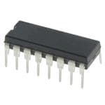
| 供应商器件封装 | 16-PDIP |
| 包装 | 管件 |
| 压摆率 | 24 V/µs |
| 双重电源电压 | +/- 5 V, +/- 9 V, +/- 12 V, +/- 15 V |
| 可用增益调整 | 1 V/V to 16 V/V |
| 商标 | Analog Devices |
| 增益带宽积 | - |
| 安装类型 | 通孔 |
| 安装风格 | Through Hole |
| 封装 | Tube |
| 封装/外壳 | 16-DIP(0.300",7.62mm) |
| 封装/箱体 | PDIP-16 |
| 工作温度 | 0°C ~ 70°C |
| 工作电源电压 | 4.5 V to 16.5 V |
| 工厂包装数量 | 25 |
| 放大器类型 | 可编程增益 |
| 最大双重电源电压 | +/- 16.5 V |
| 最大工作温度 | + 70 C |
| 最小双重电源电压 | +/- 4.5 V |
| 最小工作温度 | 0 C |
| 标准包装 | 25 |
| 电压-电源,单/双 (±) | ±4.5 V ~ 16.5 V |
| 电压-输入失调 | 400µV |
| 电流-电源 | 10mA |
| 电流-输入偏置 | 50pA |
| 电流-输出/通道 | 10mA |
| 电源电流 | 10 mA |
| 电路数 | 1 |
| 类型 | Programmable Gain Amplifier |
| 系列 | AD526 |
| 视频文件 | http://www.digikey.cn/classic/video.aspx?PlayerID=1364138032001&width=640&height=505&videoID=2245193153001http://www.digikey.cn/classic/video.aspx?PlayerID=1364138032001&width=640&height=505&videoID=2245193159001 |
| 输入补偿电压 | 700 uV |
| 输出类型 | - |
| 通道数量 | 1 Channel |


- 商务部:美国ITC正式对集成电路等产品启动337调查
- 曝三星4nm工艺存在良率问题 高通将骁龙8 Gen1或转产台积电
- 太阳诱电将投资9.5亿元在常州建新厂生产MLCC 预计2023年完工
- 英特尔发布欧洲新工厂建设计划 深化IDM 2.0 战略
- 台积电先进制程称霸业界 有大客户加持明年业绩稳了
- 达到5530亿美元!SIA预计今年全球半导体销售额将创下新高
- 英特尔拟将自动驾驶子公司Mobileye上市 估值或超500亿美元
- 三星加码芯片和SET,合并消费电子和移动部门,撤换高东真等 CEO
- 三星电子宣布重大人事变动 还合并消费电子和移动部门
- 海关总署:前11个月进口集成电路产品价值2.52万亿元 增长14.8%


PDF Datasheet 数据手册内容提取
a Software Programmable Gain Amplifier AD526 FEATURES PIN CONFIGURATION Digitally Programmable Binary Gains from 1 to 16 Two-Chip Cascade Mode Achieves Binary Gain from 1 to 256 DIG GND 1 16 A1 Gain Error: NULL 2 15 A0 0.01% Max, Gain = 1, 2, 4 (C Grade) VIN 3 14 CS 0.02% Max, Gain = 8, 16 (C Grade) NULL 4 AD526 13 CLK 0.5 ppm/8C Drift Over Temperature TOP VIEW Fast Settling Time ANALOG GND 2 5 (Not to Scale)12 A2 ANALOG GND 1 6 11 B 10 V Signal Change: 0.01% in 4.5 ms (Gain = 16) –VS 7 10 +VS Gain Change: VOUT SENSE 8 9 VOUT FORCE 0.01% in 5.6 ms (Gain = 16) Low Nonlinearity: 60.005% FSR Max (J Grade) Excellent DC Accuracy: Offset Voltage: 0.5 mV Max (C Grade) Offset Voltage Drift: 3 mV/8C (C Grade) TTL-Compatible Digital Inputs PRODUCT DESCRIPTION The AD526 is a single-ended, monolithic software program- APPLICATION HIGHLIGHTS mable gain amplifier (SPGA) that provides gains of 1, 2, 4, 8 1. Dynamic Range Extension for ADC Systems: A single and 16. It is complete, including amplifier, resistor network AD526 in conjunction with a 12-bit ADC can provide and TTL-compatible latched inputs, and requires no external 96 dB of dynamic range for ADC systems. components. 2. Gain Ranging Preamps: The AD526 offers complete digital Low gain error and low nonlinearity make the AD526 ideal for gain control with precise gains in binary steps from 1 to 16. precision instrumentation applications requiring programmable Additional gains of 32, 64, 128 and 256 are possible by cas- gain. The small signal bandwidth is 350 kHz at a gain of 16. In cading two AD526s. addition, the AD526 provides excellent dc precision. The FET- input stage results in a low bias current of 50 pA. A guaranteed ORDERING GUIDE maximum input offset voltage of 0.5 mV max (C grade) and low gain error (0.01%, G = 1, 2, 4, C grade) are accomplished using Temperature Package Package Analog Devices’ laser trimming technology. Model Range Descriptions Options To provide flexibility to the system designer, the AD526 can be AD526JN Commercial 16-Lead Plastic DIP N-16 operated in either latched or transparent mode. The force/sense AD526AD Industrial 16-Lead Cerdip D-16 configuration preserves accuracy when the output is connected AD526BD Industrial 16-Lead Cerdip D-16 to remote or low impedance loads. AD526CD Industrial 16-Lead Cerdip D-16 AD526SD Military 16-Lead Cerdip D-16 The AD526 is offered in one commercial (0(cid:176) C to +70(cid:176) C) grade, AD526SD/883B Military 16-Lead Cerdip D-16 J, and three industrial grades, A, B and C, which are specified 5962-9089401MEA* Military 16-Lead Cerdip D-16 from –40(cid:176) C to +85(cid:176) C. The S grade is specified from –55(cid:176) C to +125(cid:176) C. The military version is available processed to MIL- *Refer to official DESC drawing for tested specifications. STD 883B, Rev C. The J grade is supplied in a 16-lead plastic DIP, and the other grades are offered in a 16-lead hermetic side-brazed ceramic DIP. REV.D Information furnished by Analog Devices is believed to be accurate and reliable. However, no responsibility is assumed by Analog Devices for its use, nor for any infringements of patents or other rights of third parties One Technology Way, P.O. Box 9106, Norwood, MA 02062-9106, U.S.A. which may result from its use. No license is granted by implication or Tel: 781/329-4700 World Wide Web Site: http://www.analog.com otherwise under any patent or patent rights of Analog Devices. Fax: 781/326-8703 © Analog Devices, Inc., 1999
AD526–SPECIFICATIONS (@ V = 615 V, R = 2 kV and T = +258C unless otherwise noted) S L A AD526J AD526A AD526B/S AD526C Model Min Typ Max Min Typ Max Min Typ Max Min Typ Max Units GAIN Gain Range (Digitally Programmable) 1, 2, 4, 8, 16 1, 2, 4, 8, 16 1, 2, 4, 8, 16 1, 2, 4, 8, 16 Gain Error Gain = 1 0.05 0.02 0.01 0.01 % Gain = 2 0.05 0.03 0.02 0.01 % Gain = 4 0.10 0.03 0.02 0.01 % Gain = 8 0.15 0.07 0.04 0.02 % Gain = 16 0.15 0.07 0.04 0.02 % Gain Error Drift Over Temperature G = 1 0.5 2.0 0.5 2.0 0.5 2.0 0.5 2.0 ppm/(cid:176) C G = 2 0.5 2.0 0.5 2.0 0.5 2.0 0.5 2.0 ppm/(cid:176) C G = 4 0.5 3.0 0.5 3.0 0.5 3.0 0.5 3.0 ppm/(cid:176) C G = 8 0.5 5.0 0.5 5.0 0.5 5.0 0.5 5.0 ppm/(cid:176) C G = 16 1.0 5.0 1.0 5.0 1.0 5.0 1.0 5.0 ppm/(cid:176) C Gain Error (T to T ) MIN MAX Gain = 1 0.06 0.03 0.02 0.015 % Gain = 2 0.06 0.04 0.03 0.015 % Gain = 4 0.12 0.04 0.03 0.015 % Gain = 8 0.17 0.08 0.05 0.03 % Gain = 16 0.17 0.08 0.05 0.03 % Nonlinearity Gain = 1 0.005 0.005 0.005 0.0035 % FSR Gain = 2 0.001 0.001 0.001 0.001 % FSR Gain = 4 0.001 0.001 0.001 0.001 % FSR Gain = 8 0.001 0.001 0.001 0.001 % FSR Gain = 16 0.001 0.001 0.001 0.001 % FSR Nonlinearity (T to T ) MIN MAX Gain = 1 0.01 0.01 0.01 0.007 % FSR Gain = 2 0.001 0.001 0.001 0.001 % FSR Gain = 4 0.001 0.001 0.001 0.001 % FSR Gain = 8 0.001 0.001 0.001 0.001 % FSR Gain = 16 0.001 0.001 0.001 0.001 % FSR VOLTAGE OFFSET, ALL GAINS Input Offset Voltage 0.4 1.5 0.25 0.7 0.25 0.5 0.25 0.5 mV Input Offset Voltage Drift Over Temperature 5 20 3 10 3 10 3 10 m V/(cid:176) C Input Offset Voltage T to T 2.0 1.0 0.8 0.8 mV MIN MAX Input Offset Voltage vs. Supply (V – 10%) 80 80 84 90 dB S INPUT BIAS CURRENT Over Input Voltage Range – 10 V 50 150 50 150 50 150 50 150 pA ANALOG INPUT CHARACTERISTICS Voltage Range (Linear Operation) 610 – 12 610 – 12 610 – 12 610 – 12 V Capacitance 5 5 5 5 pF RATED OUTPUT Voltage 610 – 12 610 – 12 610 – 12 610 – 12 V Current (V = – 10 V) – 10 65 – 10 65 – 10 65 – 10 mA OUT Short-Circuit Current 15 30 15 30 15 30 15 30 mA DC Output Resistance 0.002 0.002 0.002 0.002 W Load Capacitance (For Stable Operation) 700 700 700 700 pF –2– REV. D
AD526 AD526J AD526A AD526B/S AD526C Model Min Typ Max Min Typ Max Min Typ Max Min Typ Max Units NOISE, ALL GAINS Voltage Noise, RTI 0.1 Hz to 10 Hz 3 3 3 3 m V p-p Voltage Noise Density, RTI f = 10 Hz 70 70 70 70 nV(cid:214) Hz f = 100 Hz 60 60 60 60 nV(cid:214) Hz f = 1 kHz 30 30 30 30 nV(cid:214) Hz f = 10 kHz 25 25 25 35 nV(cid:214) Hz DYNAMIC RESPONSE –3 dB Bandwidth (Small Signal) G = 1 4.0 4.0 4.0 4.0 MHz G = 2 2.0 2.0 2.0 2.0 MHz G = 4 1.5 1.5 1.5 1.5 MHz G = 8 0.65 0.65 0.65 0.65 MHz G = 16 0.35 0.35 0.35 0.35 MHz Signal Settling Time to 0.01% (D V = – 10 V) OUT G = 1 2.1 4 2.1 4 2.1 4 2.1 4 m s G = 2 2.5 5 2.5 5 2.5 5 2.5 5 m s G = 4 2.7 5 2.7 5 2.7 5 2.7 5 m s G = 8 3.6 7 3.6 7 3.6 7 3.6 7 m s G = 16 4.1 7 4.1 7 4.1 7 4.1 7 m s Full Power Bandwidth G = 1, 2, 4 0.10 0.10 0.10 0.10 MHz G = 8, 16 0.35 0.35 0.35 0.35 MHz Slew Rate G = 1, 2, 4 4 6 4 6 4 6 4 6 V/m s G = 8, 16 18 24 18 24 18 24 18 24 V/m s DIGITAL INPUTS (T to T ) MIN MAX Input Current (V = 5 V) 60 100 140 60 100 140 60 100 140 60 100 140 m A H Logic “1” 2 6 2 6 2 6 2 6 V Logic “0” 0 0.8 0 0.8 0 0.8 0 0.8 V TIMING1 (V = 0.2 V, V = 3.7 V) L H A0, A1, A2 T 50 50 50 50 ns C T 30 30 30 30 ns S T 30 30 30 30 ns H B T 50 50 50 50 ns C T 40 40 40 40 ns S T 10 10 10 30 ns H TEMPERATURE RANGE Specified Performance 0 +70 –40 +85 –40/–55 +85/+125 –40 +85 (cid:176) C Storage –65 +125 –65 +150 –65 +150 –65 +150 (cid:176) C POWER SUPPLY Operating Range 64.5 616.5 64.5 616.5 64.5 616.5 64.5 616.5 V Positive Supply Current 10 14 10 14 10 14 10 14 mA Negative Supply Current 10 13 10 13 10 13 10 13 mA PACKAGE OPTIONS Plastic (N-16) AD526JN Ceramic DIP (D-16) AD526AD AD526BD AD526SD AD526CD AD526SD/883B NOTES 1Refer to Figure 25 for definitions. FSR = Full Scale Range = 20 V. RTI = Referred to Input. Specifications subject to change without notice. Specifications shown in boldface are tested on all production units at final electrical test. All min and max specifications are guaranteed, although only those shown in boldface are tested on all production units. –3– REV. D
AD526–Typical Performance Characteristics 20 30 20 V V 6NG – 15 +258C 6NG – T – pA 15 E SWI RL = 2kV E SWI 20 @ VS = 615V RREN VIN = 0 AG 10 AG CU 10 VOLT VOLT BIAS T T 10 T PU 5 PU PU 5 T T N U U I O O 0 0 0 0 5 10 15 20 100 1k 10k 0 5 10 15 20 SUPPLY VOLTAGE – 6V LOAD RESISTANCE – V SUPPLY VOLTAGE – 6V Figure 1.Output Voltage Swing vs. Figure 2.Output Voltage Swing vs. Figure 3.Input Bias Current vs. Supply Voltage, G = 16 Load Resistance Supply Voltage 100nA 75 20 16 10 8 10nA pA VS = 615V RENT NT – 50 4 INPUT BIAS CUR110100nppAAA INPUT BIAS CURRE 25 GAIN 1 2 1 1pA 0 –60 –20 20 60 100 140 –10 –5 0 5 10 10 100 1k 10k 100k 1M 10M TEMPERATURE – 8C INPUT VOLTAGE – V FREQUENCY – Hz Figure 4.Input Bias Current vs. Figure 5.Input Bias Current vs. Input Figure 6.Gain vs. Frequency Temperature Voltage 25 100 1.0002 615V WITH 1V p-p SINE WAVE p ULL POWER RESPONSE – V p- 2110505 GAIN = 1, 2, 4 GAIN = 8, 16 WER SUPPLY REJECTION – dB 86420000 –SUPPLY +SUPPLY NORMALIZED GAIN110...009009009109 F O P 0 10 0.9998 1k 10k 100k 1M 10M 1 10 100 1k 10k 100k 1M –60 –20 20 60 100 140 FREQUENCY – Hz FREQUENCY – Hz TEMPERATURE – 8C Figure 7.Large Signal Frequency Figure 8.PSRR vs. Frequency Figure 9.Normalized Gain vs. Response Temperature, Gain = 1 –4– REV. D
AD526 1000 0.006 Hz V/ R 0.004 n S GE – – %F 0.002 A Y T T E VOL 100 NEARI 0.000 OIS NLI N O T N U –0.002 P N I 10 –0.004 10 100 1k 10k 100k –60 –20 20 60 100 140 FREQUENCY – Hz TEMPERATURE – 8C Figure 10.Noise Spectral Density Figure 11.Nonlinearity vs. Figure 12.Wideband Output Noise, Temperature, Gain = 1 G = 16 (Amplified by 10) Figure 13.Large Signal Pulse Figure 14.Small Signal Pulse Figure 15.Large Signal Pulse Response and Settling Time,* Response, G = 1 Response and Settling Time,* G = 1 G = 2 Figure 16.Small Signal Pulse Figure 17.Large Signal Pulse Figure 18.Small Signal Pulse Response, G = 2 Response and Settling Time,* Response, G = 4 G = 4 *For Settling Time Traces, 0.01% = 1/2 Vertical Division REV. D –5–
AD526 Figure 19.Large Signal Pulse Figure 20.Small Signal Pulse Figure 21.Large Signal Pulse Response and Settling Time,* G = 8 Response, G = 8 Response and Settling Time,* G = 16 –60 10 B d RTION – –70 Dedrees 5 STO N – NIC DI –80 ORTIO 0 O T M S R DI HA –90 SE –5 L A A H T P O T –100 –10 10 100 1k 10k 100k 10 100 1k 10k 100k FREQUENCY – Hz FREQUENCY – Hz Figure 22.Small Signal Pulse Figure 23.Total Harmonic Distortion Figure 24.Phase Distortion vs. Response, Gain = 16 vs. Frequency Gain = 16 Frequency, Gain = 16 100 V – E G = 2, 8 C G = 4, 16 N A PED 10 G = 1 M T I U P T U O 1 10k 100k 1M 10M FREQUENCY – Hz Figure 25.Output Impedance vs. Figure 26.Gain Change Settling Figure 27.Gain Change Settling Frequency Time,** Gain Change: 1 to 2 Time,** Gain Change 1 to 4 *For Settling Time Traces, 0.01% = 1/2 Vertical Division **Scope Traces are: Top: Output Transition; Middle: Output Settling; Bottom: Digital Input. –6– REV. D
AD526 Figure 28.Gain Change Settling Figure 29.Gain Change Settling Time,* Gain Change 1 to 8 Time,* Gain Change 1 to 16 +15V –15V 10mF 10mF +15V –15V + + 10m+F 10m+F TEKTRONIX 7000 SERIES SCOPE 7A13 PREAMP AD526 5MHz BW G = 16 OP37 900V G = 10 + 10mF 100V Vo = 160 3 e p-p +5V SHIELD NOTE: COAX CABLE 1 FT. OR LESS Figure 30.Wideband Noise Test Circuit +15V –15V 10mF 10mF + + DATA DYNAMICS 5109 +15V –15V (FOLRA TE-QTOUPIV PAULELSNET 5kV 10m+F 10m+F GENERATOR) AD526 TEKTRONIX 1pF 7000 SERIES 1pF P2OkVT. VERROR +–AD711 A–D3554 5kVVERROR 3 5 5PSMR7CHEAOzA1 PB3MEWP + G RIN 5.6kV 5kV 1 5.6kV IN6263 248 217..1845kkVVV RIN – 5pF 5kV IN6263 10m+F 1+0mF 1.25kV TSET = TMEAS2 – TX2 16 348V 50V A+D3554 –15V +15V G1 1.T2Xms 2 1.2ms 4 1.2ms 10mF 10mF 8 1.4ms + + 16 1.8ms –15V +15V Figure 31.Settling Time Test Circuit *Scope Traces are: Top: Output Transition Middle: Output Settling Bottom: Digital Input REV. D –7–
AD526 THEORY OF OPERATION TRANSPARENT MODE OF OPERATION The AD526 is a complete software programmable gain amplifier In the transparent mode of operation, the AD526 will respond (SPGA) implemented monolithically with a drift-trimmed directly to level changes at the gain code inputs (A0, A1, A2) if BiFET amplifier, a laser wafer trimmed resistor network, JFET B is tied high and both CS and CLK are allowed to float low. analog switches and TTL compatible gain code latches. After the gain codes are changed, the AD526’s output voltage A particular gain is selected by applying the appropriate gain typically requires 5.5 m s to settle to within 0.01% of the final code (see Table I) to the control logic. The control logic turns value. Figures 26 to 29 show the performance of the AD526 for on the JFET switch that connects the correct tap on the gain positive gain code changes. network to the inverting input of the amplifier; all unselected JFET gain switches are off (open). The “on” resistance of the A2 gain switches causes negligible gain error since only the A1 amplifier’s input bias current, which is less than 150 pA, actu- A0 +VS ally flows through these switches. +5V 0.1mF The AD526 is capable of storing the gain code, (latched mode), B, A0, A1, A2, under the direction of control inputs CLK and OUT CS. Alternatively, the AD526 can respond directly to gain code 16 15 14 13 12 11 10 9 FORCE changes if the control inputs are tied low (transparent mode). A1 A0 CS CLK A2 B LOGIC AND LATCHES For gains of 8 and 16, a fraction of the frequency compensation 16 8 4 2 1 capacitance (C1 in Figure 32) is automatically switched out of VOUT the circuit. This increases the amplifier’s bandwidth and im- GAIN NETWORK proves its signal settling time and slew rate. – AD526 + AMPLIFIER 1 2 3 4 5 6 7 8 OUT SENSE +VS C1 VIN 0.1mF –VS C2 VIN OUT Figure 33.Transparent Mode FORCE LATCHED MODE OF OPERATION N1 N2 The latched mode of operation is shown in Figure 34. When –VS OUT SENSE either CS or CLK go to a Logic “1,” the gain code (A0, A1, A2, B) signals are latched into the registers and held until both CS A0 and CLK return to “0.” Unused CS or CLK inputs should be tied C O 14kV to ground . The CS and CLK inputs are functionally and electri- A1 N cally equivalent. L T G = 8 A R A2 T O 3.4kV C L RESISTOR TIMING SIGNAL B HE L G = 2 NETWORK A2 S O 1kV A1 CLK GI A0 C G = 16 +VS CS 1.7kV +5V 0.1mF G = 4 DIGGNITDAL ANALOG 1kV 1A.7NkAVLOG 16 15 14 13 12 11 10 9 OFOURTCE GND2 GND1 A1 A0 CS CLK A2 B Figure 32.Simplified Schematic of the AD526 LOGIC AND LATCHES 16 8 4 2 1 VOUT GAIN NETWORK – AD526 + 1 2 3 4 5 6 7 8 OUT SENSE VIN 0.1mF –VS Figure 34.Latched Mode –8– REV. D
AD526 TIMING AND CONTROL DIGITAL FEEDTHROUGH With either CS or CLK or both held high, the AD526 gain state Table I. Logic Input Truth Table will remain constant regardless of the transitions at the A0, A1, A2 or B inputs. However, high speed logic transitions will un- Gain Code Control Condition avoidably feed through to the analog circuitry within the AD526 A2 A1 A0 B CLK (CS = 0) Gain Condition causing spikes to occur at the signal output. X X X X 1 Previous State Latched This feedthrough effect can be completely eliminated by operat- 0 0 0 1 0 1 Transparent ing the AD526 in the transparent mode and latching the gain 0 0 1 1 0 2 Transparent code in an external bank of latches (Figure 36). 0 1 0 1 0 4 Transparent To operate the AD526 using serial inputs, the configuration 0 1 1 1 0 8 Transparent shown in Figure 36 can be used with the 74LS174 replaced by a 1 X X 1 0 16 Transparent serial-in/parallel-out latch, such as the 54LS594. X X X 0 0 1 Transparent X X X 0 1 1 Latched A1 A0 A2 B +5V 0 0 0 1 1 1 Latched 0 0 1 1 1 2 Latched 1mF 0 1 0 1 1 4 Latched TIMING 74LS174 SIGNAL 0 1 1 1 1 8 Latched 1 X X 1 1 16 Latched +VS NOTE: X = Don’t Care. The specifications on page 3, in combination with Figure 35, 0.1mF give the timing requirements for loading new gain codes. OUT 16 15 14 13 12 11 10 9 FORCE A1 A0 CS CLK A2 B GAIN CODE VALID DATA LOGIC AND LATCHES INPUTS 16 8 4 2 1 TC VOUT GAIN NETWORK CLK OR CS – TS TH AD526 + TTCS == DMAINTIAM USMET CULPO TCIMK ECYCLE NGOATINE :C TOHDREE, SCHSO, ALDN DL ECVLEKL I SF O1.R4V. 1 2 3 4 5 6 7 8 OSEUNTSE TH = DATA HOLD TIME Figure 35. AD526 Timing VIN 0.1mF –VS Figure 36.Using an External Latch to Minimize Digital Feedthrough REV. D –9–
AD526 GROUNDING AND BYPASSING Utilizing the force and sense outputs of the AD526, as shown in Proper signal and grounding techniques must be applied in Figure 38, avoids signal drops along etch runs to low impedance board layout so that specified performance levels of precision loads. data acquisition components, such as the AD526, are not Table II. Logic Table for Figure 38 degraded. As is shown in Figure 37, logic and signal grounds should be V /V A2 A1 A0 OUT IN separate. By connecting the signal source ground locally to the 1 0 0 0 AD526 analog ground Pins 5 and 6, gain accuracy of the 2 0 0 1 AD526 is maintained. This ground connection should not be 4 0 1 0 corrupted by currents associated with other elements within the 8 0 1 1 system. 16 1 0 0 32 1 0 1 +15V –15V 64 1 1 0 128 1 1 1 0.1mF 0.1mF AD574 VIN 12-BIT 0.1mF 0.1mF A/D CONVERTER ANALOG ANALOG +VS –VS GROUND 1 GROUND 2 VOUT FORCE AD526 AMP VOUT GAIN SENSE NETWORK DIGITAL 1mF GROUND LATCHES AND LOGIC +5V Figure 37.Grounding and Bypassing CLK A2 A1 A0 +VS +VS +5V 0.1mF +5V 0.1mF OUT OUT 16 15 14 13 12 11 10 9 FORCE 16 15 14 13 12 11 10 9 FORCE A1 A0 CS CLK A2 B A1 A0 CS CLK A2 B LOGIC AND LATCHES LOGIC AND LATCHES 16 8 4 2 1 16 8 4 2 1 VOUT GAIN NETWORK GAIN NETWORK – – AD526 + AD526 + 1 2 3 4 5 6 7 8 OUT 1 2 3 4 5 6 7 8 OUT SENSE SENSE VIN 0.1mF 0.1mF –VS –VS Figure 38. Cascaded Operation –10– REV. D
AD526 OFFSET NULLING CASCADED OPERATION Input voltage offset nulling of the AD526 is best accomplished A cascade of two AD526s can be used to achieve binarily at a gain of 16, since the referred-to-input (RTI) offset is ampli- weighted gains from 1 to 256. If gains from 1 to 128 are needed, fied the most at this gain and therefore is most easily trimmed. no additional components are required. This is accomplished by The resulting trimmed value of RTI voltage offset typically using the B pin as shown in Figure 38. When the B pin is low, varies less than 3 m V across all gain ranges. the AD526 is held in a unity gain stage independent of the other gain code values. Note that the low input current of the AD526 minimizes RTI voltage offsets due to source resistance. OFFSET NULLING WITH A D/A CONVERTER Figure 41 shows the AD526 with offset nulling accomplished +VS with an 8-bit D/A converter (AD7524) circuit instead of the 0.1mF potentiometer shown in Figure 39. The calibration procedure is the same as before except that instead of adjusting the potenti- OUT ometer, the D/A converter corrects for the offset error. This 16 15 14 13 12 11 10 9 FORCE calibration circuit has a number of benefits in addition to elimi- A1 A0 CS CLK A2 B LOGIC AND LATCHES nating the trimpot. The most significant benefit is that calibra- tion can be under the control of a microprocessor and therefore 16 8 4 2 1 can be implemented as part of an autocalibration scheme. Sec- VOUT GAIN NETWORK ondly, dip switches or RAM can be used to hold the 8-bit word – after its value has been determined. In Figure 42 the offset null AD526 + sensitivity, at a gain of 16, is 80 m V per LSB of adjustment, 1 2 3 4 5 6 7 8 OUT which guarantees dc accuracy to the 16-bit performance level. SENSE VIN 20kV 0.1mF +VS –VS 0.1mF Figure 39. Offset Voltage Null Circuit OUT 16 15 14 13 12 11 10 9 FORCE OUTPUT CURRENT BOOSTER A1 A0 CS CLK A2 B The AD526 is rated for a full – 10 V output voltage swing into LOGIC AND LATCHES 2 kW . In some applications, the need exists to drive more cur- 16 8 4 2 1 rent into heavier loads. As shown in Figure 40, a high current VOUT GAIN NETWORK booster may be connected “inside the loop” of the SPGA to – provide the required current boost without significantly degrad- AD526 + ing overall performance. Nonlinearities, offset and gain inaccu- 1 2 3 4 5 6 7 8 OUT racies of the buffer are minimized by the loop gain of the SENSE AD526 output amplifier. +VS VIN 0.1mF ADA+5D185018V O7R 3.3MV 7.5MV –VS +VS VREF ALL BYPASS CAPACITORS ARE 0.1mF 0.1mF +VS 1kV 0.01mF MSB 10mF OUT LSB AD7524 OUT 1 – 16 15 14 13 12 11 10 9 FORCE 0.01mF CS OUT 2 AD548 WR + A1 A0 CS CLK A2 B LOGIC AND LATCHES 0.01mF 16 8 4 2 1 HOS-100 GND –VS GAIN NETWORK Figure 41.Offset Nulling Using a DAC – 0.01mF AD526 + 1 2 3 4 5 6 7 8 OUT SENSE 0.1mF VIN RL –VS Figure 40. Current Output Boosting REV. D –11–
AD526 FLOATING-POINT CONVERSION the input falls within, relative to full scale. Once the AD526 has High resolution converters are used in systems to obtain high settled to the appropriate level, then the second sample/hold accuracy, improve system resolution or increase dynamic range. amplifier can be put into hold which holds the amplified signal There are a number of high resolution converters available with while the AD7572 perform its conversion routine. The acquisi- throughput rates of 66.6 kHz that can be purchased as a single tion time for the AD585 is 3 m s, and the conversion time for the component solution; however in order to achieve higher through- AD7572 is 5 m s for a total of 8 m s, or 125 kHz. This performance put rates, alternative conversion techniques must be employed. relies on the fast settling characteristics of the AD526 after the A floating point A/D converter can improve both throughput flash autoranging (comparator) circuit quantizes the input sig- rate and dynamic range of a system. nal. A 16-bit register holds the 3-bit output from the flash autor- anger and the 12-bit output of the AD7572. In a floating point A/D converter (Figure 42), the output data is presented as a 16-bit word, the lower 12 bits from the A/D The A/D converter in Figure 42 has a dynamic range of 96 dB. converter form the mantissa and the upper 4 bits from the digi- The dynamic range of a converter is the ratio of the full-scale tal signal used to set the gain form the exponent. The AD526 input range to the LSB value. With a floating-point A/D con- programmable gain amplifier in conjunction with the compara- verter the smallest value LSB corresponds to the LSB of the tor circuit scales the input signal to a range between half scale monolithic converter divided by the maximum gain of the PGA. and full scale for the maximum usable resolution. The floating point A/D converter has a full-scale range of 5 V, a maximum gain of 16 V/V from the AD526 and a 12-bit A/D The A/D converter diagrammed in Figure 42 consists of a pair converter; this produces: of AD585 sample/hold amplifiers, a flash converter, a five-range programmable gain amplifier (the AD526) and a fast 12-bit A/D LSB = ([FSR/2N]/Gain) = ([5 V/4096]/16) = 76 m V. The converter (the AD7572). The floating-point A/D converter dynamic range in dBs is based on the log of the ratio of the achieves its high throughput rate of 125 kHz by overlapping the full-scale input range to the LSB; dynamic range = 20 log acquisition time of the first sample/hold amplifier and the set- (5 V/76 m V) = 96 dB. tling time of the AD526 with the conversion time of the A/D converter. The first sample/hold amplifier holds the signal for the flash autoranger, which determines which binary quantum –15V +15V +5V –15V +15V 10mF+ +10mF +5V +5V 10mF+ +10mF BUSY 51/6 6 30pF 50kV MSB D12 74- +5V D11 123 1C2L5OMCHKz 11/6 2 31/64 1/2 1m–1s5V+15V ADS/5H85 68pF VIN LS741–74 DD190 D8 –15V +15V 10mF+ +10mF 2.5MHz AD7572 D7 10mF+ +10mF F 10kV 68pF AD526S 47mF D6 VIN D5 S/H +5V B 74– D4 VIN AD585 A0 A1 A2 LSB LS174 D3 D2 D1 10kV –15V +15V +5V 10mF+ ++150VmRFEF 10kV 1274A1L/S4863 12 11 AAA012 LS741–74 EEE123 10kV 13 1/4 5kV 10kV AD588 45 1/4 6 NOTE: ALL BYPASS CAPACITORS ARE 0.1mF 2.5kV 10kV 190 1/4 8 12 1/4 3 1mF 1.25kV 10kV 11 10 1/6 1.25kV LM339A Figure 42.Floating-Point A/D Converter –12– REV. D
AD526 HIGH ACCURACY A/D CONVERTERS hunting during the calibration process, the reference offset and Very high accuracy and high resolution floating-point A/D con- gain codes should be different from the endpoint codes. A cali- verters can be achieved by the incorporation of offset and gain bration cycle consists of selecting whether gain or offset is to be calibration routines. There are two techniques commonly used calibrated then selecting the appropriate multiplexer channel to for calibration, a hardware circuit as shown in Figure 43 and/or apply the reference voltage to the signal channel. Once the op- a software routine. In this application the microprocessor is eration has been initiated, the counter, a 74ALS869, drives the functioning as the autoranging circuit, requiring software over- D/A converter in a linear fashion providing a small correction head; therefore, a hardware calibration technique was applied voltage to either the gain or offset trim point of the AD574. The which reduces the software burden. The software is used to set output of the A/D converter is then compared to the value pre- the gain of the AD526. In operation the signal is converted, and set in the 74ALS528 to determine a match. Once a match is if the MSB of the AD574 is not equal to a Logical 1, the gain is detected, the 74ALS528 produces a low going pulse which stops increased by binary steps, up to the maximum gain. This maxi- the counter. The code at the D/A converter is latched until the mizes the full-scale range of the conversion process and insures next calibration cycle. Calibration cycles are under the control a wide dynamic range. of the microprocessor in this application and should be imple- mented only during periods of converter inactivity. The calibration technique uses two point correction, offset and gain. The hardware is simplified by the use of programmable magnitude comparators, the 74ALS528s, which can be “burned” for a particular code. In order to prevent under or over range +5V +15V –15V 200pF 10mF 10mF + + –15V+15V MSB NROEDISUECTION AD585 7404 1mF 2 1 +15V R8 A1 AD588 A3 +5V AD7501 10kV AD526SF –15V+15V AD574 DBAUTSA R2RR15 R4 A4 –5V VVIINN12 VREF OP27 1kV R3 A2 R6 +–VVSS 0.1mF +S1Y5SV VVIINN34 WR –15V 50kV LSB 0.1mF GND DE- +5V –15V WR DECODED WR DECODED CODED ADDRESS ADDRESS ADD ADDRESS BUS 12 12 +5V CALIBRATION M7S4BALS APIDN5 2784 PVRAELSUEET +5V 5kV+5V VREF APIDN5 1858 20Rk6V2 20Rk5V 528 R72 A2 P = Q 1 3 MSB AD7628 RRRFFFBBB AAA CR1221 10kV 5Rk1V1 AD7G1A2IN GAIN 714/725 27400 BIUNFPFUETR LATCH DAC A OUT A A1 AGND 74ALS AD712 ADG221 869 RFB B R41 LSB 7475 WR C22 M7S45BPA2 L8=S Q +5V 714/725 457400 6 LSB WRCOLONTGRICOAL/B LATCH VRDEAFC B OPUINAT G1B5NDA2DAR0731k10V22 R150R9kk21VV2 A2A0DR2k78OV1F2FSET OFFSET +5V AD588 AGND NOTE: ALL BYPASS CAPACITORS ARE 0.1mF LSB +5V Figure 43.High Accuracy A/D Converter REV. D –13–
AD526 OUTLINE DIMENSIONS Dimensions shown in inches and (mm). 16-Lead Plastic 16-Lead Sided-Brazed DIP Package (N-16) Ceramic Package (D-16) 0.87 (22.1) MAX 0.430 16 9 0.25 0.31 (10.922) 99 PIN 1 1 8 (00.(0.683.925)5) (7.87) 0.3 (7.62) 0.18 (70.8.37140 6 6000..2.0054140)R 161 89 0(6.2.7635) (07.2.3970 6600..205140) 3d–0–8/ (4.57) 0 0.125 (3M.1I8N) 0(4.1.587) (00..02181) MAX PI(N02 .018.0302 6600..021540) 0.300 C11 0.018 0.100 0.033 SEATING 0.035 60.01 (7.62) (0.46) (2.54) (0.84) PLANE (0.889 60.254) REF 0.095 (2.41) 0.085 (2.159) 0.180 60.03 0.125 (4.57 60.762) (M3I.N175) 0(.10.4179 6600..01087) 0.017+–00..000023 (0B2.1.S50C40)SPELAANTIENG (00.0.21504 6 600.0.0052) (0.43 +– 00 .. 00 57 6 ) 0.700 (17.78) BSC A. S. U. N D I E T N RI P –14– REV. D
Mouser Electronics Authorized Distributor Click to View Pricing, Inventory, Delivery & Lifecycle Information: A nalog Devices Inc.: AD526BD AD526JN AD526SD AD526CDZ AD526ADZ AD526JNZ AD526BDZ AD526AD