ICGOO在线商城 > 集成电路(IC) > 数据采集 - 数字电位器 > AD5231BRUZ10
 Datasheet下载
- 型号: AD5231BRUZ10
- 制造商: Analog
- 库位|库存: xxxx|xxxx
- 要求:
| 数量阶梯 | 香港交货 | 国内含税 |
| +xxxx | $xxxx | ¥xxxx |
查看当月历史价格
查看今年历史价格
AD5231BRUZ10产品简介:
ICGOO电子元器件商城为您提供AD5231BRUZ10由Analog设计生产,在icgoo商城现货销售,并且可以通过原厂、代理商等渠道进行代购。 AD5231BRUZ10价格参考。AnalogAD5231BRUZ10封装/规格:数据采集 - 数字电位器, Digital Potentiometer 10k Ohm 1 Circuit 1024 Taps SPI Interface 16-TSSOP。您可以下载AD5231BRUZ10参考资料、Datasheet数据手册功能说明书,资料中有AD5231BRUZ10 详细功能的应用电路图电压和使用方法及教程。
AD5231BRUZ10是Analog Devices Inc.生产的一款数字电位器,属于数据采集类产品。它具有10 kΩ的电阻范围,采用SPI接口进行通信,支持8位分辨率,能够在各种需要精确电阻调节的应用场景中使用。以下是其主要应用场景:

1. 音频设备:在音频处理设备中,AD5231BRUZ10可以用于音量控制、均衡器调节等。通过数字方式调整电阻值,实现对音频信号的精确控制,避免了传统机械电位器的磨损和接触不良问题。

2. 工业自动化:在工业控制系统中,AD5231BRUZ10可用于传感器信号调理、增益调节等。例如,在温度、压力等传感器信号的放大电路中,通过数字电位器动态调整放大倍数,确保信号的稳定性和准确性。

3. 医疗设备:在医疗仪器中,如心电图机、血压计等,AD5231BRUZ10可以用于校准和调节电路参数。由于其高精度和稳定性,能够保证设备测量结果的准确性和可靠性。

4. 通信系统:在通信设备中,AD5231BRUZ10可用于射频前端的匹配网络调节、滤波器调谐等。通过数字控制电阻值,优化射频信号的传输性能,提高系统的抗干扰能力和通信质量。

5. 消费电子:在一些高端消费电子产品中,如智能音箱、耳机放大器等,AD5231BRUZ10可以用于音效调节、阻抗匹配等功能,提升用户体验。

6. 测试与测量设备:在精密测量仪器中,AD5231BRUZ10可用于校准和调节参考电压、电流等参数。其高分辨率和低漂移特性,确保了测量结果的高精度和一致性。

总之,AD5231BRUZ10凭借其高精度、低功耗和灵活的数字控制功能,广泛应用于需要精确电阻调节的各种领域,特别是在对可靠性和稳定性要求较高的场合中表现出色。
| 参数 | 数值 |
| 产品目录 | 集成电路 (IC)半导体 |
| 描述 | IC POT DGTL 1024POS 16-TSSOP数字电位计 IC IC 10-Bit EEMEM |
| 产品分类 | |
| 品牌 | Analog Devices Inc |
| 产品手册 | |
| 产品图片 |
|
| rohs | 符合RoHS无铅 / 符合限制有害物质指令(RoHS)规范要求 |
| 产品系列 | 数字电位计 IC,Analog Devices AD5231BRUZ10- |
| 数据手册 | |
| 产品型号 | AD5231BRUZ10 |
| POT数量 | Single |
| 产品目录页面 | |
| 产品种类 | 数字电位计 IC |
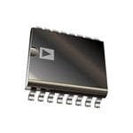
| 供应商器件封装 | 16-TSSOP |
| 包装 | 管件 |
| 商标 | Analog Devices |
| 存储器类型 | 非易失 |
| 安装类型 | 表面贴装 |
| 安装风格 | SMD/SMT |
| 容差 | 30 % |
| 封装 | Tube |
| 封装/外壳 | 16-TSSOP(0.173",4.40mm 宽) |
| 封装/箱体 | TSSOP-16 |
| 工作温度 | -40°C ~ 85°C |
| 工作电源电压 | 2.7 V |
| 工厂包装数量 | 96 |
| 弧刷存储器 | Non Volatile |
| 抽头 | 1024 |
| 接口 | 4 线 SPI(芯片选择) |
| 描述/功能 | 1024-Position Digital Potentiometer w/ Nonvolatile Memory |
| 数字接口 | SPI |
| 最大工作温度 | + 85 C |
| 最小工作温度 | - 40 C |
| 标准包装 | 96 |
| 每POT分接头 | 1024 |
| 温度系数 | 标准值 600 ppm/°C |
| 电压-电源 | 2.7 V ~ 5.5 V, ±2.25 V ~ 2.75 V |
| 电源电压-最大 | 5.5 V |
| 电源电压-最小 | 2.7 V |
| 电源电流 | 2.7 uA |
| 电路数 | 1 |
| 电阻 | 10 kOhms |
| 电阻(Ω) | 10k |
| 系列 | AD5231 |
| 缓冲刷 | Buffered |


- 商务部:美国ITC正式对集成电路等产品启动337调查
- 曝三星4nm工艺存在良率问题 高通将骁龙8 Gen1或转产台积电
- 太阳诱电将投资9.5亿元在常州建新厂生产MLCC 预计2023年完工
- 英特尔发布欧洲新工厂建设计划 深化IDM 2.0 战略
- 台积电先进制程称霸业界 有大客户加持明年业绩稳了
- 达到5530亿美元!SIA预计今年全球半导体销售额将创下新高
- 英特尔拟将自动驾驶子公司Mobileye上市 估值或超500亿美元
- 三星加码芯片和SET,合并消费电子和移动部门,撤换高东真等 CEO
- 三星电子宣布重大人事变动 还合并消费电子和移动部门
- 海关总署:前11个月进口集成电路产品价值2.52万亿元 增长14.8%


PDF Datasheet 数据手册内容提取
Nonvolatile Memory, 1024-Position Digital Potentiometer Data Sheet AD5231 FEATURES FUNCTIONAL BLOCK DIAGRAM 1024-position resolution AD5231 Nonvolatile memory maintains wiper setting CS VDD Power-on refresh with EEMEM setting CLK DAECDODRDE RERGDISATCER RDAC SDI SDI A EEMEM restore time: 140 µs typ W Full monotonic operation SERIAL GND INTERFACE EEMEM(0) B 10 kΩ, 50 kΩ, and 100 kΩ terminal resistance Permanent memory write protection SDO SDO DIGITAL Wiper setting readback REGISTER O1 Predefined linear increment/decrement instructions WP EEMEM 2 ODUIGTIOTAULT O2 RDY CONTROL BUFFER Predefined ±6 dB/step log taper increment/decrement EEMEM(1) instructions 28 BYTES VSS S3P VI ®t-oc o5m V psaintgiblele- ssuepripally i notre ±rf2a.c5e V dual-supply operation PR USER EEMEM 02739-001 Figure 1. 28 bytes extra nonvolatile memory for user-defined data 100-year typical data retention, T = 55°C 100 A RWA RWB APPLICATIONS )AB R al 75 Mechanical potentiometer replacement min Instrumentation: gain, offset adjustment No Programmable voltage to current conversion % of Programmable filters, delays, time constants D); ( 50 ( Programmable power supply B W R Low resolution DAC replacement D), 25 Sensor calibration (A W R 00 256 CODE 5(1D2ecimal) 768 1023 02739-002 Figure 2. RWA (D) and RWB (D) vs. Decimal Code GENERAL DESCRIPTION The AD5231 is a nonvolatile memory1, digitally controlled resistance between Terminals W–A and Terminals W–B. This potentiometer2 with 1024-step resolution. The device performs setting can be stored into the EEMEM and is transferred the same electronic adjustment function as a mechanical automatically to the RDAC register during system power-on. potentiometer with enhanced resolution, solid state reliability, The EEMEM content can be restored dynamically or through and remote controllability. The AD5231 has versatile programming external PR strobing, and a WP function protects EEMEM that uses a standard 3-wire serial interface for 16 modes of contents. To simplify the programming, the linear-step increment operation and adjustment, including scratchpad programming, or decrement commands can be used to move the RDAC wiper memory storing and restoring, increment/decrement, ±6 dB/step up or down, one step at a time. The ±6 dB step commands can log taper adjustment, wiper setting readback, and extra EEMEM be used to double or half the RDAC wiper setting. for user-defined information, such as memory data for other The AD5231 is available in a 16-lead TSSOP. The part is components, look-up table, or system identification information. guaranteed to operate over the extended industrial temperature In scratchpad programming mode, a specific setting can be range of −40°C to +85°C. programmed directly to the RDAC register that sets the 1 The terms nonvolatile memory and EEMEM are used interchangeably. 2 The terms digital potentiometer and RDAC are used interchangeably. Rev. D Document Feedback Information furnished by Analog Devices is believed to be accurate and reliable. However, no responsibility is assumed by Analog Devices for its use, nor for any infringements of patents or other One Technology Way, P.O. Box 9106, Norwood, MA 02062-9106, U.S.A. rights of third parties that may result from its use. Specifications subject to change without notice. No license is granted by implication or otherwise under any patent or patent rights of Analog Devices. Tel: 781.329.4700 ©2001–2013 Analog Devices, Inc. All rights reserved. Trademarks and registered trademarks are the property of their respective owners. Technical Support www.analog.com
AD5231 Data Sheet TABLE OF CONTENTS Features .............................................................................................. 1 Latched Digital Outputs ............................................................ 16 Applications ....................................................................................... 1 Advanced Control Modes ......................................................... 18 Functional Block Diagram .............................................................. 1 RDAC Structure.......................................................................... 19 General Description ......................................................................... 1 Programming the Variable Resistor ......................................... 19 Revision History ............................................................................... 2 Programming the Potentiometer Divider ............................... 20 Specifications ..................................................................................... 3 Programming Examples ............................................................ 21 Electrical Characteristics—10 kΩ, 50 kΩ, 100 kΩ Versions .. 3 Flash/EEMEM Reliability .......................................................... 22 Timing Characteristics—10 kΩ, 50 kΩ, 100 kΩ Versions ...... 5 Applications ..................................................................................... 23 Absolute Maximum Ratings ............................................................ 7 Bipolar Operation from Dual Supplies.................................... 23 ESD Caution .................................................................................. 7 High Voltage Operation ............................................................ 23 Pin Configuration and Function Descriptions ............................. 8 Bipolar Programmable Gain Amplifier ................................... 23 Typical Performance Characteristics ............................................. 9 10-Bit Bipolar DAC .................................................................... 23 Test Circuits ..................................................................................... 13 10-Bit Unipolar DAC ................................................................. 24 Theory of Operation ...................................................................... 14 Programmable Voltage Source with Boosted Output ........... 24 Scratchpad and EEMEM Programming .................................. 14 Programmable Current Source ................................................ 24 Basic Operation .......................................................................... 14 Programmable Bidirectional Current Source ......................... 25 EEMEM Protection .................................................................... 14 Resistance Scaling ...................................................................... 25 Digital Input/Output Configuration ........................................ 15 RDAC Circuit Simulation Model ............................................. 26 Serial Data Interface ................................................................... 15 Outline Dimensions ....................................................................... 27 Daisy-Chain Operation ............................................................. 15 Ordering Guide .......................................................................... 27 Terminal Voltage Operation Range ......................................... 16 Power-Up Sequence ................................................................... 16 REVISION HISTORY 3/13—Rev. C to Rev. D 5/04—Rev. 0 to Rev. A Added t ; Table 2 ............................................................................ 5 Updated formatting ............................................................ Universal WP Edits to Features, General Description, and Block Diagram ....... 1 Changes to Ordering Guide .......................................................... 27 Changes to Specifications ................................................................. 3 1/07—Rev. B to Rev. C Replaced Timing Diagrams.............................................................. 6 Updated Format .................................................................. Universal Changes to Pin Function Descriptions ........................................... 8 Changes to Dynamic Characteristics Specifications ..................... 4 Changes to Typical Performance Characteristics.......................... 9 Changes to Table 2 Footnote ............................................................ 5 Changes to Test Circuits ................................................................. 13 Changes to Table 3 ............................................................................. 7 Edits to Theory of Operation ......................................................... 14 Changes to Ordering Guide ........................................................... 27 Edits to Applications ....................................................................... 23 Updated Outline Dimensions ........................................................ 27 9/04—Rev. A to Rev. B 12/01—Revision 0: Initial Version Updated Format .................................................................. Universal Changes to Table 20 ......................................................................... 23 Changes to Resistance Scaling Section ......................................... 25 Changes to Ordering Guide ........................................................... 27 Rev. D | Page 2 of 28
Data Sheet AD5231 SPECIFICATIONS ELECTRICAL CHARACTERISTICS—10 kΩ, 50 kΩ, 100 kΩ VERSIONS V = 3 V ± 10% or 5 V ± 10%, V = 0 V, V = V , V = 0 V, −40°C < T < +85°C, unless otherwise noted. DD SS A DD B A Table 1. Parameter Symbol Conditions Min Typ1 Max Unit DC CHARACTERISTICS— RHEOSTAT MODE Resistor Differential Nonlinearity2 R-DNL R , V = NC, monotonic −1 ±1/2 +1.8 LSB WB A Resistor Integral Nonlinearity2 R-INL R ,V = NC −0.2 +0.2 LSB WB A Nominal Resistor Tolerance ΔR /R D = 0x3FF −40 +20 % AB AB Resistance Temperature Coefficient (ΔR /R )/ΔT × 106 600 ppm/°C WB WB Wiper Resistance R I = 100 µA, V = 5.5 V, 15 100 Ω W W DD code = half scale I = 100 µA, V = 3 V, 50 Ω W DD code = half scale DC CHARACTERISTICS— POTENTIOMETER DIVIDER MODE Resolution N 10 Bits Differential Nonlinearity3 DNL Monotonic, T = 25°C −1 ±1/2 +1 LSB A Monotonic, T = −40°C or +85°C −1 +1.25 LSB A Integral Nonlinearity3 INL −0.4 +0.4 LSB Voltage Divider Temperature (ΔV /V )/ΔT × 106 Code = half scale 15 ppm/°C W W Coefficient Full-Scale Error V Code = full scale −3 0 % FS WFSE Zero-Scale Error V Code = zero scale 0 1.5 % FS WZSE RESISTOR TERMINALS Terminal Voltage Range4 V V V V A, B, W SS DD Capacitance A, B5 C f = 1 MHz, measured to GND, 50 pF A, B code = half-scale Capacitance W5 C f = 1 MHz, measured to GND, 50 pF W code = half-scale Common-Mode Leakage Current5, 6 I V = V /2 0.01 1 µA CM W DD DIGITAL INPUTS AND OUTPUTS Input Logic High V With respect to GND, V = 5 V 2.4 V IH DD Input Logic Low V With respect to GND, V = 5 V 0.8 V IL DD Input Logic High V With respect to GND, V = 3 V 2.1 V IH DD Input Logic Low V With respect to GND, V = 3 V 0.6 V IL DD Input Logic High V With respect to GND, V = +2.5 V, 2.0 V IH DD V = −2.5 V SS Input Logic Low V With respect to GND, V = +2.5 V, 0.5 V IL DD V = −2.5 V SS Output Logic High (SDO, RDY) V R = 2.2 kΩ to 5 V 4.9 V OH PULL-UP (see Figure 26) Output Logic Low V I = 1.6 mA, V = 5 V 0.4 V OL OL LOGIC (see Figure 26) Input Current I V = 0 V or V ±2.5 µA IL IN DD Input Capacitance5 C 4 pF IL Output Current5 I , I V = 5 V, V = 0 V, T = 25°C 50 mA O1 O2 DD SS A V = 2.5 V, V = 0 V, T = 25°C 7 mA DD SS A Rev. D | Page 3 of 28
AD5231 Data Sheet Parameter Symbol Conditions Min Typ1 Max Unit POWER SUPPLIES Single-Supply Power Range V V = 0 V 2.7 5.5 V DD SS Dual-Supply Power Range V /V ±2.25 ±2.75 V DD SS Positive Supply Current I V = V or V = GND 2.7 10 µA DD IH DD IL Negative Supply Current I V = V or V = GND, 0.5 10 µA SS IH DD IL V = +2.5 V, V = −2.5 V DD SS EEMEM Store Mode Current I (store) V = V or V = GND, 40 mA DD IH DD IL V = GND, I ≈ 0 SS SS I (store) V = +2.5 V, V = −2.5 V −40 mA SS DD SS EEMEM Restore Mode Current7 I (restore) V = V or V = GND, 0.3 3 9 mA DD IH DD IL V = GND, I ≈ 0 SS SS I (restore) V = +2.5 V, V = −2.5 V −0.3 −3 −9 mA SS DD SS Power Dissipation8 P V = V or V = GND 0.018 0.05 mW DISS IH DD IL Power Supply Sensitivity5 P ΔV = 5 V ± 10% 0.002 0.01 %/% SS DD DYNAMIC CHARACTERISTICS5, 9 Bandwidth BW −3 dB, R = 10 kΩ/50 kΩ/ 370/85/44 kHz AB 100 kΩ Total Harmonic Distortion THD V = 1 V rms, V = 0 V, f = 1 kHz, 0.045 % W A B R = 10 kΩ AB V = 1 V rms, V = 0 V, f = 1 kHz, 0.022 % A B R = 50 kΩ, 100 kΩ AB V Settling Time t V = V , V = 0 V, 1.2/3.7/7 µs W S A DD B V = 0.50% error band, W Code 0x000 to 0x200 for R = 10 kΩ/50 kΩ/100 kΩ AB Resistor Noise Voltage e R = 5 kΩ, f = 1 kHz 9 nV/√Hz N_WB WB 1 Typical values represent average readings at 25°C and VDD = 5 V. 2 Resistor position nonlinearity error (R-INL) is the deviation from an ideal value measured between the maximum resistance and the minimum resistance wiper positions. R-DNL measures the relative step change from ideal between successive tap positions. IW ~ 50 µA @ VDD = 2.7 V and IW ~ 400 µA @ VDD = 5 V for the RAB = 10 kΩ version, IW ~ 50 µA for the RAB = 50 kΩ, and IW ~ 25 µA for the RAB = 100 kΩ version (see Figure 26). 3 INL and DNL are measured at VW with the RDAC configured as a potentiometer divider similar to a voltage output DAC. VA = VDD and VB = VSS. DNL specification limits of −1 LSB minimum are guaranteed monotonic operating condition (see Figure 27). 4 Resistor Terminal A, Resistor Terminal B, and Resistor Terminal W have no limitations on polarity with respect to each other. Dual-supply operation enables ground- referenced bipolar signal adjustment. 5 Guaranteed by design and not subject to production test. 6 Common-mode leakage current is a measure of the dc leakage from any Terminal B–W to a common-mode bias level of VDD/2. 7 EEMEM restore mode current is not continuous. Current consumed while EEMEM locations are read and transferred to the RDAC register (see Figure 23). To minimize power dissipation, a NOP Instruction 0 (0x0) should be issued immediately after Instruction 1 (0x1). 8 PDISS is calculated from (IDD × VDD) + (ISS × VSS). 9 All dynamic characteristics use VDD = +2.5 V and VSS = −2.5 V. Rev. D | Page 4 of 28
Data Sheet AD5231 TIMING CHARACTERISTICS—10 kΩ, 50 kΩ, 100 kΩ VERSIONS V = 3 V to 5.5 V, V = 0 V, and −40°C < T < +85°C, unless otherwise noted. DD SS A Table 2. Parameter Symbol Conditions Min Typ1 Max Unit INTERFACE TIMING CHARACTERISTICS2, 3 Clock Cycle Time (t ) t 20 ns CYC 1 CS Setup Time t 10 ns 2 CLK Shutdown Time to CS Rise t 1 t 3 CYC Input Clock Pulse Width t, t Clock level high or low 10 ns 4 5 Data Setup Time t From positive CLK transition 5 ns 6 Data Hold Time t From positive CLK transition 5 ns 7 CS to SDO-SPI Line Acquire t 40 ns 8 CS to SDO-SPI Line Release t 50 ns 9 CLK to SDO Propagation Delay4 t R = 2.2 kΩ, C < 20 pF 50 ns 10 P L CLK to SDO Data Hold Time t R = 2.2 kΩ, C < 20 pF 0 ns 11 P L CS High Pulse Width5 t 10 ns 12 CS High to CS High5 t 4 t 13 CYC RDY Rise to CS Fall t 0 ns 14 CS Rise to RDY Fall Time t 0.1 0.15 ms 15 Store/Read EEMEM Time6 t Applies to instructions 0x2, 0x3, and 0x9 25 ms 16 Power-On EEMEM Restore Time t R = 10 kΩ 140 μs EEMEM1 AB Dynamic EEMEM Restore Time t R = 10 kΩ 140 μs EEMEM2 AB WP High or Low to CS Fall Time t 40 ns WP CS Rise to Clock Rise/Fall Setup t 10 ns 17 Preset Pulse Width (Asynchronous) t Not shown in timing diagram 50 ns PRW Preset Response Time to Wiper Setting t PR pulsed low to refresh wiper positions 70 μs PRESP FLASH/EE MEMORY RELIABILITY Endurance7 100 kCycles Data Retention8 100 Years 1 Typical values represent average readings at 25°C and VDD = 5 V. 2 Guaranteed by design and not subject to production test. 3 See timing diagrams (Figure 3 and Figure 4) for location of measured values. All input control voltages are specified with tR = tF = 2.5 ns (10% to 90% of 3 V) and timed from a voltage level of 1.5 V. Switching characteristics are measured using both VDD = 3 V and VDD = 35 V. 4 Propagation delay depends on the value of VDD, RPULL-UP, and CL. 5 Valid for commands that do not activate the RDY pin. 6 RDY pin low only for Instructions 2, 3, 8, 9, 10, and the PR hardware pulse: CMD_2, 3 ~ 20 ms; CMD_8 ~ 1 ms; CMD_9, 10 ~ 0.12 ms. Device operation at TA = −40°C and VDD < 3 V extends the EEMEM store time to 35 ms. 7 Endurance is qualified to 100,000 cycles per JEDEC Standard 22, Method A117 and measured at −40°C, +25°C, and +85°C; typical endurance at +25°C is 700,000 cycles. 8 Retention lifetime equivalent at junction temperature (TJ) = 55°C per JEDEC Standard 22, Method A117. Retention lifetime based on an activation energy of 0.6 eV derates with junction temperature, as shown in Figure 45 in the Flash/EEMEM Reliability section. Rev. D | Page 5 of 28
AD5231 Data Sheet Timing Diagrams CPHA = 1 CS t12 t3 t13 t2 t1 CPOLC =L K1 t5 Bt243 B0 t17 t7 t6 HIGH HIGH OR LOW OR LOW SDI B23–MSB B0–LSB t8 t10 t11 t9 SDO B24* B23–MSB B0–LSB t14 t15 t16 RDY *NTHOET CDPEOFILN =E D1, MBIUCTR ONOCORMNTARLOLYL LLESRB COOFM CMHAANRDA CATLEIGRN PSR TEHVEIO INUCSOLYM TINRGA NDSAMTAIT TTOED T.HE POSITIVE EDGE OF THE CLOCK. 02739-003 Figure 3. CPHA = 1 Timing Diagram CPHA = 0 CS t12 t1 t3 t13 CPOLC =L K0 t2 B23 t5 B0 t17 t4 t6 HIGH HIGH OR LOW OR LOW SDI B23–MSB IN B0–LSB t8 t10 t11 t9 SDO B23–MSB OUT B0–LSB * t7 t14 t15 t16 RDY *NTHOET CDPEOFILN =E D0, MBIUCTR ONOCORMNTARLOLYL LMESRB C OOFM CMHAANRDA ACLTIEGRN SP RTEHVEI OINUCSOLMY IRNEGC DEAIVTEAD T.O THE POSITIVE EDGE OF THE CLOCK. 02739-004 Figure 4. CPHA = 0 Timing Diagram Rev. D | Page 6 of 28
Data Sheet AD5231 ABSOLUTE MAXIMUM RATINGS T = 25°C, unless otherwise noted. A Table 3. Stresses above those listed under Absolute Maximum Ratings Parameters Ratings may cause permanent damage to the device. This is a stress V to GND –0.3 V, +7 V rating only; functional operation of the device at these or any DD V to GND +0.3 V, −7 V other conditions above those indicated in the operational SS V to V 7 V section of this specification is not implied. Exposure to absolute DD SS V , V , V to GND V − 0.3 V, V + 0.3 V maximum rating conditions for extended periods may affect A B W SS DD A–B, A–W, B–W device reliability. Intermittent1 ±20 mA Continuous ±2 mA ESD CAUTION Digital Input and Output Voltage −0.3 V, V + 0.3 V DD to GND Operating Temperature Range2 −40°C to +85°C Maximum Junction Temperature 150°C (T max) J Storage Temperature −65°C to +150°C Reflow Soldering Peak Temperature 260°C Time at Peak Temperature 20 sec to 40 sec Thermal Resistance 150°C/W Junction-to-Ambient (θ ),TSSOP-16 JA Junction-to-Case (θ ), TSSOP-16 28°C/W JC Package Power Dissipation (T max − T )/θ J A JA 1 Maximum terminal current is bounded by the maximum current handling of the switches, maximum power dissipation of the package, and maximum applied voltage across any two of the A, B, and W terminals at a given resistance. 2 Includes programming of nonvolatile memory. Rev. D | Page 7 of 28
AD5231 Data Sheet PIN CONFIGURATION AND FUNCTION DESCRIPTIONS O1 1 16 O2 CLK 2 15 RDY SDI 3 14 CS SDO 4 AD5231 13 PR TOP VIEW GND 5 (Not to Scale) 12 WP VSS 6 11 VDD T 7 10 A B 8 9 W 02739-005 Figure 5. Pin Configuration Table 4. Pin Function Descriptions Pin No. Mnemonic Description 1 O1 Nonvolatile Digital Output 1. ADDR = 0x1, data bit position D0. For example, to store O1 high, the data bit format is 0x310001. 2 CLK Serial Input Register Clock Pin. Shifts in one bit at a time on positive clock edges. 3 SDI Serial Data Input Pin. Shifts in one bit at a time on positive clock CLK edges. MSB loaded first. 4 SDO Serial Data Output Pin. Serves readback and daisy-chain functions. Command 9 and Command 10 activate the SDO output for the readback function, delayed by 24 or 25 clock pulses, depending on the clock polarity before and after the data-word (see Figure 3, Figure 4, and Table 7). In other commands, the SDO shifts out the previously loaded SDI bit pattern, delayed by 24 or 25 clock pulses depending on the clock polarity (see Figure 3 and Figure 4). This previously shifted-out SDI can be used for daisy-chaining multiple devices. Whenever SDO is used, a pull-up resistor in the range of 1 kΩ to 10 kΩ is needed. 5 GND Ground Pin. Logic ground reference. 6 V Negative Supply. Connect to 0 V for single-supply applications. If V is used in dual-supply applications, it must be SS SS able to sink 40 mA for 25 ms when storing data to EEMEM. 7 T Reserved for factory testing. Connect to V or V . DD SS 8 B Terminal B of RDAC. 9 W Wiper Terminal of RDAC. ADDR (RDAC) = 0x0. 10 A Terminal A of RDAC. 11 V Positive Power Supply Pin. DD 12 WP Optional Write Protect Pin. When active low, WP prevents any changes to the present contents, except PR and Instruction 1 and Instruction 8 and refreshes the RDAC register from EEMEM. Execute a NOP instruction before returning to WP high. Tie WP to VDD, if not used. 13 PR Optional Hardware Override Preset Pin. Refreshes the scratchpad register with current contents of the EEMEM register. Factory default loads midscale 51210 until EEMEM is loaded with a new value by the user. PR is activated at the logic high transition. Tie PR to VDD, if not used. 14 CS Serial Register Chip Select Active Low. Serial register operation takes place when CS returns to logic high. 15 RDY Ready. Active-high open-drain output. Identifies completion of Instructions 2, 3, 8, 9, 10, and PR. 16 O2 Nonvolatile Digital Output 2. ADDR = 0x1, data bit position D1. For example, to store O2 high, the data bit format is 0x310002. Rev. D | Page 8 of 28
Data Sheet AD5231 TYPICAL PERFORMANCE CHARACTERISTICS 1.5 2.0 VDD = 5V, VSS = 0V TA = +85°C 1.5 1.0 1.0 TA = –40°C B) LS 0.5 B) 0.5 INL ERROR ( 0 TA = –40°C TA = +25°C R-DNL (LS–0.50 TA = +85°C TA = +25°C –1.0 –0.5 –1.5 –1.00 128 256 38C4ODE5 (1D2ecima6l4)0 768 896 1024 02739-006 –2.00 128 256 38C4ODE 5(D1e2cima6l)40 768 896 1024 02739-009 Figure 6. INL vs. Code, TA = −40°C, +25°C, +85°C Overlay, RAB = 10 kΩ Figure 9. R-DNL vs. Code, TA = −40°C, +25°C, +85°C Overlay, RAB = 10 kΩ 2.0 3000 VDD = 5V, VSS = 0V VDD = 5.5V, VSS = 0V 1.5 m/°C) 2500 TA = –40°C TO +85°C 1.0 p R (LSB) 0.5 TA = –40°C EMPCO (p 2000 RO 0 E T 1500 R D E O DNL –0.5 TA = +85°C AT M 1000 –1.0 TA = +25°C OST E RH 500 –1.5 –2.0 0 0 128 256 38C4ODE 5(1D2ecima6l4)0 768 896 1024 02739-007 0 128 256 38C4ODE 5(1D2ecima6l4)0 768 896 1024 02739-010 Figure 7. DNL vs. Code, TA = −40°C, +25°C, +85°C Overlay, RAB = 10 kΩ Figure 10. (∆RWB/RWB)/∆T × 106 1.0 100 0.5 VDD = 5V, VSS = 0V O (ppm/°C) 80 TVVVADBA D === =–02 4V.500.05°VVC, TVOSS + =85 0°VC C MP 60 SB) TA = +85°C E TE R-INL (L 0 TA = +25°C ER MOD 40 T E 20 M –0.5 TIO N E 0 T TA = –40°C PO –1.0 –20 0 128 256 38C4ODE 5(1D2ecima6l4)0 768 896 1024 02739-008 0 128 256 38C4ODE 5(1D2ecima6l4)0 768 896 1024 02739-011 Figure 8. R-INL vs. Code, TA = −40°C, +25°C, +85°C Overlay, RAB = 10 kΩ Figure 11. (∆VW/VW)/∆T × 106 Rev. D | Page 9 of 28
AD5231 Data Sheet 60 2 VDD = 2.7V, VSS = 0V f–3dB = 37kHz, RAB = 10kΩ TA = 25°C 0 50 –2 40 –4 R (Ω)W 30 GAIN (dB) ––68 f–3dBf– =3d 4B4 =k H8z5,k RHAzB, R =A 1B0 =0 k5Ω0kΩ 20 –10 –12 10 –14 VVADD =/ V1SmSV = r±m2s.5V D = MIDSCALE 00 128 256 38C4ODE5 (1D2ecima6l4)0 768 896 1024 02739-012 –161k 10kFREQUENCY (Hz)100k 1M 02739-015 Figure 12. Wiper On Resistance vs. Code Figure 15. −3 dB Bandwidth vs. Resistance (Figure 32) 4 0.12 VDD/VSS = ±2.5V VA = 1V rms 0.10 3 IDD @ VDD/VSS = 5V/0V NT (µA) 2 OISE (%)00..0068 E N CURR 1 ISS @ VDD/VSS = 5V/0V THD + 0.04 RAB = 10kΩ 0 50kΩ 0.02 IDD @ VDD/VSS = 2.7V/0V ISS @ VDD/VSS = 2.7V/0V 100kΩ –1–40 –20 0 TEM2P0ERATUR40E (°C) 60 80 100 02739-013 00.01 0.1 FREQUEN1CY (kHz) 10 100 02739-016 Figure 13. IDD vs. Temperature, RAB = 10 kΩ Figure 16. Total Harmonic Distortion vs. Frequency 0.25 0 VDD = 5V CODE = 0x200 VSS = 0V –5 0.20 –10 0x100 –15 0x80 (mA) 0.15 FULL-SCALE N (dB) ––2250 0x40 IDD 0.10 GAI –30 0x20 0x10 ZERO-SCALE –35 0x08 0.05 –40 MIDSCALE –45 0x04 0x02 0x01 00 2 CLO4CK FREQ6UENCY (M8Hz) 10 12 02739-014 –501k 10k FREQU1E0N0CkY (Hz) 1M 10M 02739-017 Figure 14. IDD vs. Clock Frequency, RAB = 10 kΩ Figure 17. Gain vs. Frequency vs. Code, RAB = 10 kΩ (Figure 32) Rev. D | Page 10 of 28
Data Sheet AD5231 0 CODE = 0x200 VDD = 5V –10 0x100 10900 VVAB == 02.V25V VA 0x80 –20 B) 0x40 VW N (d –30 0x20 GAI 0x10 EXVPAELCUTEED –40 0x08 MIDSCALE 0x04 0.5V/DIV 0x02 –50 10 0x01 0% –601k 10kFREQUENCY (Hz)100k 1M 02739-018 100µs/DIV 02739-021 Figure 18. Gain vs. Frequency vs. Code, RAB = 50 kΩ (Figure 32) Figure 21. Power-On Reset, VA = 2.25 V, VB = 0 V, Code = 1010101010B 0 2.55 CODE = 0x200 VDD/VSS = 5V/0V CODE = 0x200 TO 0x1FF –10 0x100 2.53 0x80 –20 0x40 N (dB) –30 0x20 (V)UT 2.51 RRAABB == 1500kkΩΩ GAI 0x10 VO 2.49 RAB = 100kΩ –40 0x08 0x04 2.47 –50 0x02 0x01 –601k 10kFREQUENCY (Hz)100k 1M 02739-019 2.450 5 10TIME (µs)15 20 25 02739-022 Figure 19. Gain vs. Frequency vs. Code, RAB = 100 kΩ (Figure 32) Figure 22. Midscale Glitch Energy, Code 0x200 to 0x1FF 80 RAB = 100kΩ 70 5V/DIV RAB = 50kΩ CS 60 RAB = 10kΩ B)50 d CLK – R (40 5V/DIV R S P 30 SDI 5V/DIV 20 10 VDD = 5.0V ±100mV AC IDD VSS = 0V, VA = 5V, VB = 0V 20mA/DIV 0100MEASURED1k AT VW WIFT1R0HEk CQOUDEEN C=Y 01x0(H200zk0) 1M 10M 02739-020 4ms/DIV 02739-023 Figure 20. PSRR vs. Frequency Figure 23. IDD vs. Time when Storing Data to EEMEM Rev. D | Page 11 of 28
AD5231 Data Sheet 100 VA = VB = OPEN TA = 25°C 5V/DIV CS mA) 10 (X A M CLK WB_ RAB = 10kΩ 5V/DIV —I 1 L A C TI RAB = 50kΩ SDI RE 5V/DIV HEO 0.1 T RAB = 100kΩ IDD* 2mA/DIV 0.01 *SIIFNU SIPNTPSRLTUYRC UCTCUIOTRNIRO E1N N( R0T E (RNAEODTP EU) ERISMN SEE4 MXmTE)Os.C/ DMUITIVNEIDM UIMMM PEODWIAETRE LCYO ANFSTUEMRPTION 02739-024 0 128 256 38C4ODE 5(D12ecima6l)40 768 896 1024 02739-025 Figure 24. IDD vs. Time when Restoring Data from EEMEM Figure 25. IWB_MAX vs. Code Rev. D | Page 12 of 28
Data Sheet AD5231 TEST CIRCUITS Figure 26 to Figure 35 define the test conditions used in the specifications. NC 5V DUT A IW W VIN OP279 VOUT B W NC = NO CVOMNSNECT 02739-026 OFFGSNEDT OFFSAET BDIAUST B 02739-031 Figure 26. Resistor Position Nonlinearity Error Figure 31. Noninverting Gain (Rheostat Operation; R-INL, R-DNL) DUT V+ = VDD A +15V A W 1LSB = V+/2N VIN DUT W V+ OFFSET B OP42 VOUT B VMS 02739-027 GND +2.5V –15V 02739-032 Figure 27. Potentiometer Divider Nonlinearity Error (INL, DNL) Figure 32. Gain vs. Frequency NC 0.1V DUT DUT RSW= ISW A W VW IW A W CODE = 0x000 VMS2 + B VMS1 RW = [VMS1 – VMS2]/IW 02739-028 NCB = NO COISNWNECT VBIAS –0.1V 02739-033 Figure 28. Wiper Resistance Figure 33. Incremental On Resistance NC VA V+ = VDD ±10% VDD A ICM V+ VDD A W PSRR (dB) = 20 log ΔΔVVMDDS DUT W B VMS PSS (%/%) =ΔΔVVMDDS%% 02739-029 VSS GNDNCBNC = NO CONNVECCMT 02739-034 Figure 29. Power Supply Sensitivity (PSS, PSRR) Figure 34. Common-Mode Leakage Current A DUT B 200µA IOL 5V OFFGSNEDT VIN W OP279 VOUT TO OUTPPUINT CL VOVOORHL ((MMAINX)) OFFSET BIAS 02739-030 50pF 200µA IOH 02739-057 Figure 30. Inverting Gain Figure 35. Load Circuit for Measuring VOH and VOL (The diode bridge test circuit is equivalent to the application circuit with RPULL-UP of 2.2 kΩ) Rev. D | Page 13 of 28
AD5231 Data Sheet THEORY OF OPERATION BASIC OPERATION The AD5231 digital potentiometer is designed to operate as a true variable resistor replacement device for analog signals that The basic mode of setting the variable resistor wiper position remain within the terminal voltage range of VSS < VTERM < VDD. (programming the scratchpad register) is accomplished by The basic voltage range is limited to VDD − VSS < 5.5 V. The loading the serial data input register with Instruction 11 (0xB), digital potentiometer wiper position is determined by the Address 0, and the desired wiper position data. When the RDAC register contents. proper wiper position is determined, the user can load the serial data input register with Instruction 2 (0x2), which stores the The RDAC register acts as a scratchpad register, allowing as wiper position data in the EEMEM register. After 25 ms, the many value changes as necessary to place the potentiometer wiper position is permanently stored in the nonvolatile wiper in the correct position. The scratchpad register can be memory. Table 5 provides a programming example listing the programmed with any position value using the standard SPI sequence of serial data input (SDI) words with the serial data serial interface mode by loading the complete representative output appearing at the SDO pin in hexadecimal format. data-word. Once a desirable position is found, this value can be stored in an EEMEM register. Thereafter, the wiper position is Table 5. Set and Store RDAC Data to EEMEM Register always restored to that position for subsequent power-up. SDI SDO Action The storing of EEMEM data takes approximately 25 ms; during 0xB00100 0xXXXXXX Writes data 0x100 to the RDAC this time, the shift register is locked, preventing any changes register, Wiper W moves to 1/4 from taking place. The RDY pin pulses low to indicate the full-scale position. completion of this EEMEM storage. 0x20XXXX 0xB00100 Stores RDAC register content into the EEMEM register. The following instructions facilitate the user’s programming At system power-on, the scratchpad register is automatically needs (see Table 7 for details): refreshed with the value previously stored in the EEMEM 0. Do nothing. register. The factory-preset EEMEM value is midscale, but 1. Restore EEMEM content to RDAC. it can be changed by the user thereafter. 2. Store RDAC setting to EEMEM. During operation, the scratchpad (RDAC) register can be refreshed with the EEMEM register data with Instruction 1 3. Store RDAC setting or user data to EEMEM. (0x1) or Instruction 8 (0x8). The RDAC register can also be 4. Decrement 6 dB. refreshed with the EEMEM register data under hardware 5. Decrement 6 dB. control by pulsing the PR pin. The PR pulse first sets the wiper 6. Decrement one step. at midscale when brought to logic zero, and then, on the positive transition to logic high, it reloads the RDAC wiper 7. Decrement one step. register with the contents of EEMEM. 8. Reset EEMEM content to RDAC. Many additional advanced programming commands are 9. Read EEMEM content from SDO. available to simplify the variable resistor adjustment process 10. Read RDAC wiper setting from SDO. (see Table 7). For example, the wiper position can be changed one step at a time using the increment/decrement instruction or 11. Write data to RDAC. by 6 dB with the shift left/right instruction. Once an increment, 12. Increment 6 dB. decrement, or shift instruction has been loaded into the shift 13. Increment 6 dB. register, subsequent CS strobes can repeat this command. 14. Increment one step. A serial data output SDO pin is available for daisy-chaining and for readout of the internal register contents. 15. Increment one step. EEMEM PROTECTION SCRATCHPAD AND EEMEM PROGRAMMING The write protect (WP) pin disables any changes to the The scratchpad RDAC register directly controls the position of scratchpad register contents, except for the EEMEM setting, the digital potentiometer wiper. For example, when the scratchpad which can still be restored using Instruction 1, Instruction 8, register is loaded with all zeros, the wiper is connected to and the PR pulse. Therefore, WP can be used to provide a Terminal B of the variable resistor. The scratchpad register is a standard logic register with no restriction on the number of hardware EEMEM protection feature. To disable WP, it is changes allowed, but the EEMEM registers have a program recommended to execute a NOP instruction before returning erase/write cycle limitation (see the Flash/EEMEM Reliability WP to logic high. section). Rev. D | Page 14 of 28
Data Sheet AD5231 DIGITAL INPUT/OUTPUT CONFIGURATION returns high, the serial data-word is decoded according to the instructions in Table 7. The command bits (Cx) control the All digital inputs are ESD-protected, high input impedance that operation of the digital potentiometer. The address bits (Ax) can be driven directly from most digital sources. Active at logic determine which register is activated. The data bits (Dx) are the low, PR and WP must be tied to V if they are not used. No DD values that are loaded into the decoded register. internal pull-up resistors are present on any digital input pins. The SDO and RDY pins are open-drain digital outputs that The AD5231 has an internal counter that counts a multiple of need pull-up resistors only if these functions are used. A resistor 24 bits (a frame) for proper operation. For example, AD5231 value in the range of 1 kΩ to 10 kΩ is a proper choice that works with a 48-bit word, but it cannot work properly with a balances the dissipation and switching speed. 23-bit or 25-bit word. In addition, AD5231 has a subtle feature that, if CS is pulsed without CLK and SDI, the part repeats the The equivalent serial data input and output logic is shown in previous command (except during power-up). As a result, care Figure 36. The open-drain output SDO is disabled whenever must be taken to ensure that no excessive noise exists in the chip-select CS is in logic high. ESD protection of the digital CLK or CS line that might alter the effective number of bits inputs is shown in Figure 37 and Figure 38. (ENOB) pattern. Also, to prevent data from mislocking (due PR WP to noise, for example), the counter resets if the count is not a VALID multiple of four when CS goes high. COMMAND COMMAND 5V PROCESSOR The SPI interface can be used in two slave modes: CPHA = 1, AND ADDRESS COUNTER DECODE CPOL = 1 and CPHA = 0, CPOL = 0. CPHA and CPOL refer to RPULL-UP the control bits that dictate SPI timing in the following CLK SERIAL MicroConverters® and microprocessors: ADuC812/ADuC824, REGISTER M68HC11, and MC68HC16R1/916R1. SDO CS GND DAISY-CHAIN OPERATION SDI AD5231 02739-035 Tusheed s teor iraela dda ttah eo ucotpnutet nptisn o (fS tDheO w) ispeervr esse tttwinog p aunrdp oEsEeMs. EItM ca n be Figure 36. Equivalent Digital Input-Output Logic values using Instruction 10 and Instruction 9, respectively. The VDD remaining instructions (0 to 8, 11 to 15) are valid for daisy- chaining multiple devices in simultaneous operations. Daisy- chaining minimizes the number of port pins required from INPUT LOGIC 300Ω the controlling IC (see Figure 39). The SDO pin contains an PINS open-drain N-Ch FET that requires a pull-up resistor if this function is used. As shown in Figure 39, users need to tie the SDO pin of one package to the SDI pin of the next package. GND 02739-036 Upuslelr-su pm riegshits tnoere adn tdo tihnec rceaapsaec tihtiev ec lloocakd ipnegr iaotd t,h bee ScDauOse t oth SeD I Figure 37. Equivalent ESD Digital Input Protection interface might require additional time delay between sub- VDD sequent packages. When two AD5231s are daisy-chained, 48 bits of data are required. The first 24 bits go to U2 and the second 24 bits go to U1. The CS should be kept low until all INPUT 300Ω 48 bits are clocked into their respective serial registers. The CS WP is then pulled high to complete the operation. +V GND 02739-037 AD5231 R2kPΩ AD5231 Figure 38. Equivalent WP Input Protection µC SDI U1 SDO SDI U2 SDO SERIAL DATA INTERFACE CS CLK CS CLK T(ShDeI A, SDD5O23, 1C cSo, nantadi nCsL aK 4)-.w Iti rues SesP Ia- 2co4m-bpita steibrilea ld digatitaa-lw ionrtedr face 02739-038 loaded MSB first. The format of the SPI-compatible word is Figure 39. Daisy-Chain Configuration Using SDO shown in Table 6. The chip-select CS pin must be held low until the complete data-word is loaded into the SDI pin. When CS Rev. D | Page 15 of 28
AD5231 Data Sheet TERMINAL VOLTAGE OPERATION RANGE POWER-UP SEQUENCE The AD5231’s positive V and negative V power supplies Because there are diodes to limit the voltage compliance at the DD SS define the boundary conditions for proper 3-terminal digital A, B, and W terminals (Figure 40), it is important to power potentiometer operation. Supply signals present on the A, B, V /V first before applying any voltage to Terminal A, DD SS and W terminals that exceed V or V are clamped by the Terminal B, and Terminal W. Otherwise, the diode is forward- DD SS internal forward-biased diodes (see Figure 40). biased such that V /V are powered unintentionally and DD SS might affect the rest of the user’s circuit. The ideal power-up The ground pin of the AD5231 device is primarily used as a sequence is GND, V , V , digital inputs, and V /V /V . The digital ground reference, which needs to be tied to the common DD SS A B W order of powering V , V , V , and digital inputs is not ground of the PCB. The digital input control signals to the A B W important as long as they are powered after V /V . AD5231 must be referenced to the device ground pin (GND) DD SS and satisfy the logic level defined in the Specifications section. Regardless of the power-up sequence and the ramp rates of the An internal level-shift circuit ensures that the common-mode power supplies, once V /V are powered, the power-on preset DD SS voltage range of the three terminals extends from V to V , remains effective, which restores the EEMEM value to the SS DD regardless of the digital input level. RDAC register. VDD LATCHED DIGITAL OUTPUTS A pair of digital outputs, O1 and O2, is available on the AD5231. These outputs provide a nonvolatile Logic 0 or Logic 1 A setting. O1 and O2 are standard CMOS logic outputs, shown in W Figure 41. These outputs are ideal to replace the functions often provided by DIP switches. In addition, they can be used to drive B other standard CMOS logic-controlled parts that need an occasional setting change. Pin O1 and Pin O2 default to Logic 1, VSS 02739-039 and they can drive uVDpD to 50 mA of load at 5 V/25°C. Figure 40. Maximum Terminal Voltages Set by VDD and VSS OUTPUTS O1 AND O2 PINS GND 02739-040 Figure 41. Logic Outputs O1 and O2 Rev. D | Page 16 of 28
Data Sheet AD5231 In Table 6, command bits are C0 to C3, address bits are A3 to A0, Data Bit D0 to Data Bit D9 are applicable to RDAC, and D0 to D15 are applicable to EEMEM. Table 6. AD5231 24-Bit Serial Data-Word MSB Command Byte 0 Data Byte 1 Data Byte 0 LSB RDAC C3 C2 C1 C0 0 0 0 0 X X X X X X D9 D8 D7 D6 D5 D4 D3 D2 D1 D0 EEMEM C3 C2 C1 C0 A3 A2 A1 A0 D15 D14 D13 D12 D11 D10 D9 D8 D7 D6 D5 D4 D3 D2 D1 D0 Command instruction codes are defined in Table 7. Table 7. Command/Operation Truth Table1, 2, 3 Command Byte 0 Data Byte 1 Data Byte 0 Instruction B23 B16 B15 B8 B7 B0 Number C3 C2 C1 C0 A3 A2 A1 A0 X … D9 D8 D7 … D0 Operation 0 0 0 0 0 X X X X X … X X X … X NOP: Do nothing. See Table 15. 1 0 0 0 1 0 0 0 0 X … X X X … X Restore EEMEM(0) contents to RDAC register. This command leaves the device in the read program power state. To return the part to the idle state, perform NOP instruction 0. See Table 15. 2 0 0 1 0 0 0 0 0 X … X X X … X Store Wiper Setting: Store RDAC setting to EEMEM(0). See Table 14. 34 0 0 1 1 A3 A2 A1 A0 D15 … D8 D7 … D0 Store contents of Data Bytes 0 and 1 (total 16 bits) to EEMEM (ADDR 1to ADDR 15). See Table 17. 45 0 1 0 0 0 0 0 0 X … X X X … X Decrement RDAC by 6 dB. 55 0 1 0 1 X X X X X … X X X … X Same as Instruction 4. 65 0 1 1 0 0 0 0 0 X … X X X … X Decrement RDAC by 1 position. 75 0 1 1 1 X X X X X … X X X … X Same as Instruction 6. 8 1 0 0 0 X X X X X … X X X … X Reset: Restore RDAC with EEMEM (0) value. 9 1 0 0 1 A3 A2 A1 A0 X … X X X … X Read EEMEM (ADDR 0 to ADDR 15) from SDO output in the next frame. See Table 18. 10 1 0 1 0 0 0 0 0 X … X X X … X Read RDAC wiper setting from SDO output in the next frame. See Table 19. 11 1 0 1 1 0 0 0 0 X … D9 D8 D7 … D0 Write contents of Data Bytes 0 and 1 (total 10 bits) to RDAC. See Table 13. 125 1 1 0 0 0 0 0 0 X … X X X … X Increment RDAC by 6 dB. See Table 16. 135 1 1 0 1 X X X X X … X X X … X Same as Instruction 12. 145 1 1 1 0 0 0 0 0 X … X X X … X Increment RDAC by 1 position. See Table 14. 155 1 1 1 1 X X X X X … X X X … X Same as Instruction 14. 1 The SDO output shifts out the last 24 bits of data clocked into the serial register for daisy-chain operation. Exception: for any instruction following Instruction 9 or Instruction 10, the selected internal register data is present in Data Byte 0 and Data Byte 1. The instruction following 9 and 10 must also be a full 24-bit data-word to completely clock out the contents of the serial register. 2 The RDAC register is a volatile scratchpad register that is refreshed at power-on from the corresponding nonvolatile EEMEM register. 3 Execution of these operations takes place when the CS strobe returns to logic high. 4 Instruction 3 writes two data bytes (16 bits of data) to EEMEM. In the case of 0 addresses, only the last 10 bits are valid for wiper position setting. 5 The increment, decrement, and shift instructions ignore the contents of the shift register Data Byte 0 and Data Byte 1. Rev. D | Page 17 of 28
AD5231 Data Sheet ADVANCED CONTROL MODES makes the left-shift function as ideal a logarithmic adjustment as possible. The AD5231 digital potentiometer includes a set of user programming features to address the wide number of The right-shift 4 and 5 instructions are ideal only if the LSB is 0 applications for these universal adjustment devices. (ideal logarithmic = no error). If the LSB is 1, the right-shift function generates a linear half-LSB error, which translates to Key programming features include: a number-of-bits dependent logarithmic error, as shown in • Scratchpad programming to any desirable values Figure 42. The plot shows the error of the odd numbers of bits • Nonvolatile memory storage of the scratchpad RDAC register for the AD5231. value in the EEMEM register Table 8. Detail Left-Shift and Right-Shift Functions • Increment and decrement instructions for the RDAC wiper for 6 dB Step Increment and Decrement register Left-Shift Right-Shift • Left and right bit shift of the RDAC wiper register to achieve 00 0000 0000 11 1111 1111 00 0000 0001 01 1111 1111 ±6 dB level changes 00 0000 0010 00 1111 1111 • 28 extra bytes of user-addressable nonvolatile memory 00 0000 0100 00 0111 1111 Linear Increment and Decrement Instructions 00 0000 1000 00 0011 1111 The increment and decrement instructions (14, 15, 6, and 7) are Left-Shift 00 0001 0000 00 0001 1111 Right-Shift useful for linear step-adjustment applications. These commands (+6 dB/step) 00 0010 0000 00 0000 1111 (–6 dB/step) simplify microcontroller software coding by allowing the 00 0100 0000 00 0000 0111 controller to send just an increment or decrement command to 00 1000 0000 00 0000 0011 the device. 01 0000 0000 00 0000 0001 10 0000 0000 00 0000 0000 For an increment command, executing Instruction 14 with the 11 1111 1111 00 0000 0000 proper address automatically moves the wiper to the next 11 1111 1111 00 0000 0000 resistance segment position. Instruction 15 performs the same function, except that the address does not need to be specified. Actual conformance to a logarithmic curve between the data contents in the RDAC register and the wiper position for each Logarithmic Taper Mode Adjustment right-shift 4 and 5 command execution contains an error only Four programming instructions produce logarithmic taper for odd numbers of bits. Even numbers of bits are ideal. The increment and decrement of the wiper. These settings are graph in Figure 42 shows plots of Log_Error [20 × log 10 activated by the 6 dB increment and 6 dB decrement (error/code)] for the AD5231. For example, Code 3 Log_Error instructions (12, 13, 4, and 5). For example, starting at zero = 20 × log (0.5/3) = −15.56 dB, which is the worst case. The 10 scale, executing the increment Instruction 12 eleven times plot of Log_Error is more significant at the lower codes. moves the wiper in 6 dB per step from 0% to full scale, R . The AB 0 6 dB increment instruction doubles the value of the RDAC register contents each time the command is executed. When the wiper position is near the maximum setting, the last 6 dB –20 increment instruction causes the wiper to go to the full-scale 1023 code position. Further 6 dB per increment instructions do not change the wiper position beyond its full scale. B) d –40 ( The 6 dB step increments and 6 dB step decrements are achieved by shifting the bit internally to the left or right, respectively. The following information explains the nonideal –60 ±6 dB step adjustment under certain conditions. Table 8 illustrates the operation of the shifting function on the RDAC roepgeirsatetiro dna. tNa obtiets t. hEaatc thh eta lbelfet- rsohwift r 1e2p raensedn 1t3s ain ssutcrucecstsioivnes swheifrte –800 0.1 0.2 CO0.D3E (F0.r4om 10 .t5o 1002.63 by0 2.7.0 ×0 1.803) 0.9 1.0 1.1 02739-041 modified such that, if the data in the RDAC register is equal to Figure 42. Plot of Log_Error Conformance for Odd Numbers of Bits Only zero and the data is shifted left, the RDAC register is then set to (Even Numbers of Bits Are Ideal) Code 1. Similarly, if the data in the RDAC register is greater than or equal to midscale and the data is shifted left, then the data in the RDAC register is automatically set to full scale. This Rev. D | Page 18 of 28
Data Sheet AD5231 Using Additional Internal Nonvolatile EEMEM SWA A The AD5231 contains additional user EEMEM registers for storing any 16-bit data such as memory data for other compo- SW(2N–1) nents, look-up tables, or system identification information. Table 9 provides an address map of the internal storage registers RDAC RS SW(2N–2) W shown in the functional block diagram as EEMEM1, EEMEM2, WIPER REGISTER and 28 bytes (14 addresses × 2 bytes each) of user EEMEM. AND DECODER Table 9. EEMEM Address Map RS SW(1) Address EEMEM for… 0000 RDAC1, 2 RS SW(0) 0001 O1 and O23 RS = RAB/2N 0010 USER14 DIGITAL 0…0 11 U…S ER2 COCILMRAICTRUTITIETYDR YFOR SWB B 02739-042 1110 USER13 Figure 43. Equivalent RDAC Structure (Patent Pending) 1111 USER14 Table 10. Nominal Individual Segment Resistor (R) 1 RDAC data stored in EEMEM location is transferred to the RDAC register at S power-on, or when Instruction 1, Instruction 8, or PR are executed. Device 10 kΩ 50 kΩ 100 kΩ 2 Execution of Instruction 1 leaves the device in the read mode power Resolution Version Version Version consumption state. After the last Instruction 1 is executed, the user should 10-Bit 9.8 Ω 48.8 Ω 97.6 Ω perform a NOP, Instruction 0 to return the device to the low power idling state. 3 O1 and O2 data stored in EEMEM locations is transferred to the PROGRAMMING THE VARIABLE RESISTOR corresponding digital register at power-on, or when Instruction 1 and Instruction 8 are executed. Rheostat Operation 4 USERx are internal nonvolatile EEMEM registers available to store 16-bit information using Instruction 3 and restore the contents using Instruction 9. The nominal resistance of the RDAC between Terminal A and RDAC STRUCTURE Terminal B, R , is available with 10 kΩ, 50 kΩ, and 100 kΩ AB with 1024 positions (10-bit resolution). The final digit(s) of the The patent-pending RDAC contains multiple strings of equal part number determine the nominal resistance value, for resistor segments with an array of analog switches that act as the example, 10 kΩ = 10; 50 kΩ = 50; 100 kΩ = C. wiper connection. The number of positions is the resolution of the device. The AD5231 has 1024 connection points, allowing it The 10-bit data-word in the RDAC latch is decoded to select to provide better than 0.1% settability resolution. Figure 43 one of the 1024 possible settings. The following discussion shows an equivalent structure of the connections among the describes the calculation of resistance RWB at different codes of a three terminals of the RDAC. The SWA and SWB are always on, 10 kΩ part. For VDD = 5 V, the wiper’s first connection starts at while the switches SW(0) to SW(2N−1) are on one at a time, Terminal B for data 0x000. RWB(0) is 15 Ω because of the wiper depending on the resistance position decoded from the data resistance, and because it is independent of the nominal bits. Because the switch is not ideal, there is a 15 Ω wiper resistance. The second connection is the first tap point where resistance, RW. Wiper resistance is a function of supply voltage RWB (1) becomes 9.7 Ω + 15 Ω = 24.7 Ω for data 0x001. The and temperature. The lower the supply voltage or the higher the third connection is the next tap point representing RWB (2) = temperature, the higher the resulting wiper resistance. Users 19.4 Ω + 15 Ω = 34.4 Ω for data 0x002 and so on. Each LSB data should be aware of the wiper resistance dynamics if accurate value increase moves the wiper up the resistor ladder until the prediction of the output resistance is needed. last tap point is reached at RWB (1023) = 10,005 Ω. See Figure 43 for a simplified diagram of the equivalent RDAC circuit. When R is used, Terminal A can be left floating or tied to the wiper. WB Rev. D | Page 19 of 28
AD5231 Data Sheet 100 The general transfer equation for this operation is RWA RWB al R)AB75 RWB(D)=1012042−4D×RAB +RW (2) n mi For example, the output resistance values in Table 12 are set for o N of the RDAC latch codes with VDD = 5 V (applies to RAB = 10 kΩ % D); ( 50 digital potentiometers). ( RWB Table 12. RWA(D) at Selected Codes for RAB = 10 kΩ (D), 25 D (DEC) RWA(D) (Ω) Output State WA 1023 24.7 Full scale R 512 5015 Midscale 1 10005 1 LSB 00 256 CODE5 (1D2ecimal) 768 1023 02739-043 0 10,015 Zero scale Figure 44. RWA(D) and RWB(D) vs. Decimal Code The typical distribution of R from device to device matches AB The general equation that determines the programmed output tightly when they are processed in the same batch. When resistance between W and B is devices are processed at a different time, device-to-device matching becomes process-lot dependent and exhibits a −40% D RWB(D)=1024×RAB +RW (1) to +20% variation. The change in RAB with temperature has a 600 ppm/°C temperature coefficient. where: PROGRAMMING THE POTENTIOMETER DIVIDER D is the decimal equivalent of the data contained in the RDAC Voltage Output Operation register. The digital potentiometer can be configured to generate an R is the nominal resistance between Terminal A and AB output voltage at the wiper terminal that is proportional to the Terminal B. input voltages applied to Terminal A and Terminal B. For R is the wiper resistance. W example, connecting Terminal A to 5 V and Terminal B to For example, the output resistance values in Table 11 are set ground produces an output voltage at the wiper that can be any for the given RDAC latch codes with V = 5 V (applies to DD value from 0 V to 5 V. Each LSB of voltage is equal to the R = 10 kΩ digital potentiometers). AB voltage applied across Terminals A–B divided by the 2N position resolution of the potentiometer divider. Table 11. R (D) at Selected Codes for R = 10 kΩ WB AB D (DEC) R (D) (Ω) Output State Because AD5231 can also be supplied by dual supplies, the WB 1023 10,005 Full scale general equation defining the output voltage at VW with respect 512 50,015 Midscale to ground for any given input voltages applied to Terminal A 1 24.7 1 LSB and Terminal B is 0 15 Zero scale (wiper contact resistor) D V (D)= ×V +V (3) Note that, in the zero-scale condition, a finite wiper resistance W 1024 AB B of 15 Ω is present. Care should be taken to limit the current Equation 3 assumes that V is buffered so that the effect of W flow between W and B in this state to no more than 20 mA to wiper resistance is minimized. Operation of the digital avoid degradation or possible destruction of the internal switches. potentiometer in divider mode results in more accurate Like the mechanical potentiometer that the RDAC replaces, the operation over temperature. Here, the output voltage is AD5231 part is totally symmetrical. The resistance between dependent on the ratio of the internal resistors and not the Wiper W and Terminal A also produces a digitally controlled absolute value; therefore, the drift improves to 15 ppm/°C. complementary resistance, R . Figure 44 shows the symmetrical There is no voltage polarity restriction between Terminal A, WA programmability of the various terminal connections. When Terminal B, and Terminal W as long as the terminal voltage RWA is used, Terminal B can be left floating or tied to the wiper. (VTERM) stays within VSS < VTERM < VDD. Setting the resistance value for R starts at a maximum value WA of resistance and decreases as the data loaded in the latch is increased in value. Rev. D | Page 20 of 28
Data Sheet AD5231 PROGRAMMING EXAMPLES Table 17. Storing Additional User Data in EEMEM The following programming examples illustrate a typical SDI SDO Action sequence of events for various features of the AD5231. See 0x32AAAA 0xXXXXXX Stores data 0xAAAA in the extra Table 7 for the instructions and data-word format. The EEMEM location USER1. (Allowable to instruction numbers, addresses, and data appearing at SDI address in 14 locations with a and SDO pins are in hexadecimal format. maximum of 16 bits of data.) 0x335555 0x32AAAA Stores data 0x5555 in the extra Table 13. Scratchpad Programming EEMEM location USER2. (Allowable to SDI SDO Action address in 14 locations with a maximum of 16 bits of data.) 0xB00100 0xXXXXXX Writes data 0x100 into RDAC register, Wiper W moves to 1/4 full-scale position. Table 18. Reading Back Data from Memory Locations Table 14. Incrementing RDAC Followed by Storing the SDI SDO Action Wiper Setting to EEMEM 0x92XXXX 0xXXXXXX Prepares data read from EEMEM(2) location. SDI SDO Action 0x00XXXX 0x92AAAA NOP Instruction 0 sends a 24-bit word 0xB00100 0xXXXXXX Writes data 0x100 into RDAC register, out of SDO, where the last 16 bits Wiper W moves to 1/4 full-scale contain the contents in the EEMEM(2) position. location. The NOP command ensures 0xE0XXXX 0xB00100 Increments RDAC register by one to that the device returns to the idle 0x101. power dissipation state. 0xE0XXXX 0xE0XXXX Increments RDAC register by one to 0x102. Continue until desired wiper Table 19. Reading Back Wiper Settings position is reached. SDI SDO Action 0x20XXXX 0xXXXXXX Stores RDAC register data into EEMEM(0). Optionally tie WP to GND 0xB00200 0xXXXXXX Writes RDAC to midscale. to protect EEMEM values. 0xC0XXXX 0xB00200 Doubles RDAC from midscale to full scale (left-shift instruction). The EEMEM value for the RDAC can be restored by power-on, 0xA0XXXX 0xC0XXXX Prepares reading wiper setting from by strobing the PR pin, or by programming, as shown in RDAC register. Table 15. 0xXXXXXX 0xA003FF Reads back full-scale value from SDO. Table 15. Restoring the EEMEM Value to the RDAC Register SDI SDO Action 0x10XXXX 0xXXXXXX Restores the EEMEM(0) value to the RDAC register. 0x00XXXX 0x10XXXX NOP. Recommended step to minimize power consumption. Table 16. Using Left-Shift by One to Increment 6 dB Step SDI SDO Action 0xC0XXXX 0xXXXXXX Moves the wiper to double the present data contained in the RDAC register. Rev. D | Page 21 of 28
AD5231 Data Sheet FLASH/EEMEM RELIABILITY Lifetime Specification (A117) at a specific junction temperature (T = 55°C). As part of this qualification procedure, the J The Flash/EE memory array on the AD5231 is fully qualified Flash/EE memory is cycled to its specified endurance limit, for two key Flash/EE memory characteristics, namely Flash/EE described previously, before data retention is characterized. memory cycling endurance and Flash/EE memory data This means that the Flash/EE memory is guaranteed to retain retention. its data for its full specified retention lifetime every time the Endurance quantifies the ability of the Flash/EE memory to be Flash/EE memory is reprogrammed. It should also be noted cycled through many program, read, and erase cycles. In real that retention lifetime, based on an activation energy of 0.6 eV, terms, a single endurance cycle is composed of four derates with T, as shown in Figure 45. For example, the data is J independent, sequential events. These events are defined as retained for 100 years at 55°C operation, but reduces to 15 years • Initial page erase sequence at 85°C operation. Beyond these limits, the part must be reprogrammed so that the data can be restored. • Read/verify sequence • Byte program sequence 300 • Second read/verify sequence 250 During reliability qualification, Flash/EE memory is cycled from 0x000 to 0x3FF until a first fail is recorded signifying the s)200 endurance limit of the on-chip Flash/EE memory. ar e Y As indicated in the Specifications section, the AD5231 Flash/EE ON (150 ANALOG DEVICES memory endurance qualification has been carried out in ENTI TAYTP TIJC A= L5 5P°ECRFORMANCE accordance with JEDEC Specification A117 over the industrial RET100 temperature range of −40°C to +85°C. The results allow the specification of a minimum endurance figure over supply and 50 temperature of 100,000 cycles, with an endurance figure of 700,000 cycles being typical of operation at 25°C. 0 Retention quantifies the ability of the Flash/EE memory to 40 50 TJ6J0UNCTIO7N0TEMPE8R0ATURE9(0°C) 100 110 02739-044 retain its programmed data over time. Again, the AD5231 has Figure 45. Flash/EE Memory Data Retention been qualified in accordance with the formal JEDEC Retention Rev. D | Page 22 of 28
Data Sheet AD5231 APPLICATIONS BIPOLAR OPERATION FROM DUAL SUPPLIES VDD The AD5231 can be operated from dual supplies ±2.5 V, which U2 V+ eonpaebraletiso cno. nAtrCo ls iogfn garlos uans dh irgehfe ares nVcDeDd/ VacS Ss ciganna blse oarp bpilpieodl adri r ectly AD523A1 WB OP2V17–7 R2 C2.C2pVFO across Terminal A to Terminal B with output taken from Vi A B –KVi A2 VSS Terminal W. See Figure 46 for a typical circuit connection. W VDD R1 +2.5V U1 V+ AD5231 OP2177 V– VDD SS CS VDD µCGND SMCOLSKI SCDLKI A ±1.25V p-p ±2.5V p-p A VSS 02739-047 W Figure 48. Bipolar Programmable Gain Amplifier GND B In the simpler (and much more usual) case where K = 1, AD5231 a pair of matched resistors can replace U1. Equation 4 can be VSS D = MIDSCALE Figure 46. Bipolar Operation from Dual Supplies –2.5V 02739-045 simplVifOied= to1 +R2×2D2 −1 (5) V R1 1024 I HIGH VOLTAGE OPERATION Table 20 shows the result of adjusting D with A2 configured as a The digital potentiometer can be placed directly in the feedback unity gain, a gain of 2, and a gain of 10. The result is a bipolar or input path of an op amp for gain control, provided that the amplifier with linearly programmable gain and 1024-step voltage across Terminals A–B, Terminals W–A, or Terminals resolution. W–B does not exceed |5 V|. When high voltage gain is needed, users should set a fixed gain in an op amp operated at a higher Table 20. Result of Bipolar Gain Amplifier voltage and let the digital potentiometer control the adjustable D R1 = ∞, R2 = 0 R1 = R2 R2 = 9 × R1 input. Figure 47 shows a simple implementation. 0 −1 −2 −10 R 2R 256 −0.5 −1 −5 512 0 0 0 CC 2.2pF 768 0.5 1 5 1023 0.992 1.984 9.92 15V 5V – V+ 10-BIT BIPOLAR DAC A A1 VO AD5231 W + V– 0VTO15V If the circuit in Figure 48 is changed with the input taken from a B 02739-046 vDoAltCag cea rne fbeer erneaclei zaendd. CAo2m copnafriegdu troed t haes cao bnuvfefnert,i oan 1a0l- DbiAt Cbi,p tohliasr Figure 47. 15 V Voltage Span Control circuit offers comparable resolution but not the precision BIPOLAR PROGRAMMABLE GAIN AMPLIFIER because of the wiper resistance effects. Degradation of the nonlinearity and temperature coefficient is prominent near There are several ways to achieve bipolar gain. Figure 48 shows both ends of the adjustment range. On the other hand, this one versatile implementation. Digital potentiometer U1 sets the circuit offers a unique nonvolatile memory feature that in some adjustment range; the wiper voltage V can, therefore, be W2 cases outweighs any shortfall in precision. programmed between V and −KV at a given U2 setting. For i i linear adjustment, configure A2 as a noninverting amplifier and The output of this circuit is the transfer function becomes 2D V = 2 −1×V (6) V R2 D O 1024 REF O = 1+ × 2 ×(1+K)−K (4) V R1 1024 I where: K is the ratio of R /R that is set by U1. WB WA D is the decimal equivalent of the input code. Rev. D | Page 23 of 28
AD5231 Data Sheet +5V PROGRAMMABLE CURRENT SOURCE A programmable current source can be implemented with the U1 V+ circuit shown in Figure 52. AD5231 W AD8V55–2 VO +5V +5V B A A2 R R 2 U1 VINVOUT +2.5VREF +5V –2.5VREF –5V VIN 0V TO (2.048V + VL) 3 6 TRIM SLEEP VOUT B GND V+ REF191 ADR421 AD8V55–2 GND C1µ1F W Figure 4A9.1 10–-B5Vit Bipolar DAC 02739-048 4 AD5231 V++5V A– 1R0S2Ω OP1177 10-BIT UNIPOLAR DAC –2.048VTOVL V–U2 + VL bFuigfuferre i5s 0n seheodweds tao u dnriipvoel vara r1i0o-ubsi tl eDadAsC. using AD5231. The –5V 100RΩL IL 02739-051 5V Figure 52. Programmable Current Source AD5231 REF191 is a unique low supply, headroom precision reference 1 U1 VINVOUT 3 A 5V that can deliver the 20 mA needed at 2.048 V. The load current W is simply the voltage across Terminals B–W of the digital V+ GND B AD8601 VO potentiometer divided by RS: V– 2 AD1582 V ×D A1 02739-049 IL = RSRE×F1024 (7) Figure 50. 10-Bit Unipolar DAC The circuit is simple, but be aware that there are two issues. PROGRAMMABLE VOLTAGE SOURCE WITH First, dual-supply op amps are ideal because the ground BOOSTED OUTPUT potential of REF191 can swing from −2.048 V at zero scale to VL at full scale of the potentiometer setting. Although the circuit For applications that require high current adjustment, such as a works under single-supply, the programmable resolution of the laser diode driver or tunable laser, a boosted voltage source can system is reduced. Second, the voltage compliance at V is L be considered (see Figure 51). limited to 2.5 V or equivalently a 125 Ω load. Should higher voltage compliance be needed, users can consider digital VIN VOUT potentiometers AD5260, AD5280, and AD7376. Figure 53 AD5231 2N7002 SIGNALCC RBIAS shows an alternate circuit for high voltage compliance. AW U2 IL To achieve higher current, such as when driving a high power V+ B AD8601 LD LED, the user can replace the UI with an LDO, reduce RS, and add a resistor in series with the digital potentiometer’s V– 02739-058 Ain ctereramseins atlh. eT chuisr rleimnti tasd tjhues tpmoetennt trieosmoleutteiro’sn c. urrent and Figure 51. Programmable Booster Voltage Source In this circuit, the inverting input of the op amp forces the V OUT to be equal to the wiper voltage set by the digital potentiometer. The load current is then delivered by the supply via the N-Ch FET N. N power handling must be adequate to dissipate 1 1 (V − V ) × I power. This circuit can source a maximum of i O L 100 mA with a 5 V supply. For precision applications, a voltage reference such as ADR421, ADR03, or ADR370 can be applied at Terminal A of the digital potentiometer. Rev. D | Page 24 of 28
Data Sheet AD5231 PROGRAMMABLE BIDIRECTIONAL CURRENT RESISTANCE SCALING SOURCE The AD5231 offers 10 kΩ, 50 kΩ, and 100 kΩ nominal For applications that require bidirectional current control or resistance. For users who need lower resistance but want to higher voltage compliance, a Howland current pump can be a maintain the number of adjustment steps, they can parallel solution. If the resistors are matched, the load current is multiple devices. For example, Figure 54 shows a simple scheme (R2A+R2B) of paralleling two AD5231s. To adjust half the resistance linearly per step, users need to program both devices coherently IL = RR21B ×VW (8) with the same settings and tie the terminals as shown. R1 R2 150kΩ 15kΩ A1 A2 +15V 1C0p1F LDB1 W1 B2 W2 02739-053 – Figure 54. Reduce Resistance by Half with Linear Adjustment Characteristics V+ OP2177 In voltage diver mode, by paralleling a discrete resistor as +2.5V +15V + V– A2 R502ΩB shown in Figure 55, a proportionately lower voltage appears at A AD5231 + V+ –15V Terminals A–B. This translates into a finer degree of precision, B W OP2177 VL because the step size at Terminal W is smaller. The voltage can –2.5V – V– 15R01kΩ 14R.925AkΩ RL be found as follows: 500Ω A1–15V IL 02739-052 VW(D) = R3(R+ABR//R/2/)R2 × 10D24 × VDD (10) Figure 53. Programmable Bidirectional Current Source AB R2B, in theory, can be made as small as necessary to achieve the current needed within the A2 output current-driving capability. R3 In this circuit, OP2177 delivers ±5 mA in both directions, and A the voltage compliance approaches 15 V. It can be shown that R2 R1 W the output impRe1d'aRn2cBe i(sR 1+R2A) B 02739-059 Z = (9) Figure 55. Lowering the Nominal Resistance O R1R2'−R1'(R2A+R2B) Figure 54 and Figure 55 show that the digital potentiometers Z can be infinite if resistors R1 and R2 match precisely with R1 O change steps linearly. On the other hand, pseudo log taper and R2A + R2B,respectively. On the other hand, Z can be O adjustment is usually preferred in applications such as audio negative if the resistors are not matched. As a result, C1, in the control. Figure 56 shows another type of resistance scaling. In range of 1 pF to 10 pF, is needed to prevent oscillation from the this configuration, the smaller the R2 with respect to R1, the negative impedance. more the pseudo log taper characteristic of the circuit behaves. A VO R1 W B R2 02739-055 Figure 56. Resistor Scaling with Pseudo Log Adjustment Characteristics Rev. D | Page 25 of 28
AD5231 Data Sheet RDAC CIRCUIT SIMULATION MODEL The following code provides a macro model net list for the 10 kΩ RDAC: The internal parasitic capacitances and the external load dominates the ac characteristics of the RDACs. The −3 dB .PARAM D = 1024, RDAC = 10E3 bandwidth of the AD5231BRU10 (10 kΩ resistor) measures * 370 kHz at half scale when configured as a potentiometer .SUBCKT DPOT (A, W, B) * divider. Figure 15 provides the large signal BODE plot charac- CA A 0 50E-12 teristics. A parasitic simulation mode is shown in Figure 57. RWA A W {(1-D/1024)* RDAC + 15} RDAC CW W 0 50E-12 10kΩ A B RWB W B {D/1024 * RDAC + 15} CB B 0 50E-12 CA CB 50pF 50pF * .ENDS DPOT W 5C0pWF 02739-056 Figure 57. RDAC Circuit Simulation Model for RDAC = 10 kΩ Rev. D | Page 26 of 28
Data Sheet AD5231 OUTLINE DIMENSIONS 5.10 5.00 4.90 16 9 4.50 6.40 4.40 BSC 4.30 1 8 PIN 1 1.20 MAX 0.15 0.20 0.05 0.09 0.75 0.30 8° 0.60 B0.S6C5 0.19 SPELAANTIENG 0° 0.45 COPLANARITY 0.10 COMPLIANT TO JEDEC STANDARDS MO-153-AB Figure 58. 16-Lead Thin Shrink Small Outline Package [TSSOP] (RU-16) Dimensions shown in millimeters ORDERING GUIDE Model1 R (kΩ) Temperature Range Package Description Package Option Ordering Quantity AB AD5231BRU10 10 −40°C to +85°C 16-Lead TSSOP RU-16 96 AD5231BRU10-REEL7 10 −40°C to +85°C 16-Lead TSSOP RU-16 1,000 AD5231BRUZ10 10 −40°C to +85°C 16-Lead TSSOP RU-16 96 AD5231BRUZ10-REEL7 10 −40°C to +85°C 16-Lead TSSOP RU-16 1,000 AD5231BRUZ50 50 −40°C to +85°C 16-Lead TSSOP RU-16 96 AD5231BRUZ50-REEL7 50 −40°C to +85°C 16-Lead TSSOP RU-16 1,000 AD5231BRU100 100 −40°C to +85°C 16-Lead TSSOP RU-16 96 AD5231BRU100-REEL7 100 −40°C to +85°C 16-Lead TSSOP RU-16 1,000 AD5231BRUZ100 100 −40°C to +85°C 16-Lead TSSOP RU-16 96 AD5231BRUZ100-RL7 100 −40°C to +85°C 16-Lead TSSOP RU-16 1,000 1 Z = RoHS Compliant Part. Rev. D | Page 27 of 28
AD5231 Data Sheet NOTES Purchase of licensed I2C components of Analog Devices or one of its sublicensed Associated Companies conveys a license for the purchaser under the Philips I2C Patent Rights to use these components in an I2C system, provided that the system conforms to the I2C Standard Specification as defined by Philips. ©2001–2013 Analog Devices, Inc. All rights reserved. Trademarks and registered trademarks are the property of their respective owners. D02739-0-3/13(D) Rev. D | Page 28 of 28
Mouser Electronics Authorized Distributor Click to View Pricing, Inventory, Delivery & Lifecycle Information: A nalog Devices Inc.: AD5231BRUZ10-REEL7 AD5231BRUZ10 AD5231BRU10 AD5231BRUZ100-RL7 AD5231BRUZ50-REEL7 AD5231BRU100 AD5231BRUZ100 AD5231BRUZ50