ICGOO在线商城 > 集成电路(IC) > 数据采集 - 数字电位器 > AD5162BRMZ10
 Datasheet下载
- 型号: AD5162BRMZ10
- 制造商: Analog
- 库位|库存: xxxx|xxxx
- 要求:
| 数量阶梯 | 香港交货 | 国内含税 |
| +xxxx | $xxxx | ¥xxxx |
查看当月历史价格
查看今年历史价格
AD5162BRMZ10产品简介:
ICGOO电子元器件商城为您提供AD5162BRMZ10由Analog设计生产,在icgoo商城现货销售,并且可以通过原厂、代理商等渠道进行代购。 AD5162BRMZ10价格参考¥12.33-¥23.19。AnalogAD5162BRMZ10封装/规格:数据采集 - 数字电位器, Digital Potentiometer 10k Ohm 2 Circuit 256 Taps SPI Interface 10-MSOP。您可以下载AD5162BRMZ10参考资料、Datasheet数据手册功能说明书,资料中有AD5162BRMZ10 详细功能的应用电路图电压和使用方法及教程。
AD5162BRMZ10 是由 Analog Devices Inc.(ADI)生产的一款数字电位器,属于数据采集类产品。其主要应用场景包括以下几种:

 1. 可编程增益放大器 (PGA)
   - AD5162BRMZ10 可用于设计可编程增益放大器。通过调整数字电位器的阻值,可以动态改变放大器的增益,从而适应不同的输入信号范围。这种应用常见于音频设备、传感器信号调理电路和工业自动化系统中。

 2. 电压基准调节
   - 在需要精确电压调节的场合,AD5162BRMZ10 可作为分压器使用,通过数字接口调整输出电压。例如,在电源管理电路中,可以用来动态调节参考电压,以满足不同负载的需求。

 3. 滤波器调谐
   - 数字电位器可用于有源滤波器的设计中,通过调整电阻值来改变滤波器的截止频率或品质因数(Q 值)。这种功能在音频处理、通信系统和信号处理领域非常有用。

 4. 传感器校准
   - 在工业控制和测量系统中,传感器输出可能需要进行校准。AD5162BRMZ10 可以通过软件控制实现电阻值的微调,从而补偿传感器的非线性误差或温度漂移。

 5. 用户界面调整
   - 在消费电子或嵌入式设备中,AD5162BRMZ10 可用于提供用户可调的功能,例如音量控制、亮度调节或对比度设置。相比传统机械电位器,数字电位器具有更高的可靠性和更长的使用寿命。

 6. 电机控制
   - 在电机驱动电路中,AD5162BRMZ10 可用于调整电流限值或速度设定值。通过数字接口实时修改电阻值,可以实现对电机性能的精确控制。

 7. 电池管理
   - 在电池管理系统中,AD5162BRMZ10 可用于调节充电电流或电压阈值。这种灵活性有助于优化电池的充电效率和延长其寿命。

 特点总结:
- 低功耗:适合便携式和电池供电设备。
- 高分辨率:提供精细的电阻调节能力。
- SPI 接口:易于与微控制器或其他数字系统集成。
- 小型封装:节省电路板空间,适合紧凑型设计。

总之,AD5162BRMZ10 的应用场景广泛,涵盖消费电子、工业自动化、通信设备、医疗仪器等领域,能够为各种需要动态电阻调节的应用提供高效解决方案。
| 参数 | 数值 |
| 产品目录 | 集成电路 (IC)半导体 |
| 描述 | IC POT DUAL 10K 256POS 10-MSOP数字电位计 IC IC Dual 8-Bit SPI |
| DevelopmentKit | EVAL-AD5162SDZ |
| 产品分类 | |
| 品牌 | Analog Devices |
| 产品手册 | |
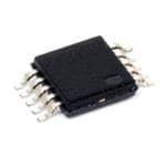
| 产品图片 |
|
| rohs | 符合RoHS无铅 / 符合限制有害物质指令(RoHS)规范要求 |
| 产品系列 | 数字电位计 IC,Analog Devices AD5162BRMZ10- |
| 数据手册 | |
| 产品型号 | AD5162BRMZ10 |
| POT数量 | Dual |
| 产品目录页面 | |
| 产品种类 | 数字电位计 IC |
| 供应商器件封装 | 10-MSOP |
| 包装 | 管件 |
| 商标 | Analog Devices |
| 存储器类型 | 易失 |
| 安装类型 | 表面贴装 |
| 安装风格 | SMD/SMT |
| 容差 | 20 % |
| 封装 | Tube |
| 封装/外壳 | 10-TFSOP,10-MSOP(0.118",3.00mm 宽) |
| 封装/箱体 | MSOP-10 |
| 工作温度 | -40°C ~ 125°C |
| 工作电源电压 | 5.5 V |
| 工厂包装数量 | 50 |
| 弧刷存储器 | Volatile |
| 抽头 | 256 |
| 接口 | 3 线串行(芯片选择) |
| 数字接口 | SPI |
| 最大工作温度 | + 125 C |
| 最小工作温度 | - 40 C |
| 标准包装 | 50 |
| 每POT分接头 | 256 |
| 温度系数 | 35 PPM / C |
| 电压-电源 | 2.7 V ~ 5.5 V |
| 电源电压-最大 | 5.5 V |
| 电源电压-最小 | 2.7 V |
| 电源电流 | 3.5 uA |
| 电路数 | 2 |
| 电阻 | 10 kOhms |
| 电阻(Ω) | 10k |
| 系列 | AD5162 |
| 配用 | /product-detail/zh/AD5162EVAL/AD5162EVAL-ND/653771 |


- 商务部:美国ITC正式对集成电路等产品启动337调查
- 曝三星4nm工艺存在良率问题 高通将骁龙8 Gen1或转产台积电
- 太阳诱电将投资9.5亿元在常州建新厂生产MLCC 预计2023年完工
- 英特尔发布欧洲新工厂建设计划 深化IDM 2.0 战略
- 台积电先进制程称霸业界 有大客户加持明年业绩稳了
- 达到5530亿美元!SIA预计今年全球半导体销售额将创下新高
- 英特尔拟将自动驾驶子公司Mobileye上市 估值或超500亿美元
- 三星加码芯片和SET,合并消费电子和移动部门,撤换高东真等 CEO
- 三星电子宣布重大人事变动 还合并消费电子和移动部门
- 海关总署:前11个月进口集成电路产品价值2.52万亿元 增长14.8%


PDF Datasheet 数据手册内容提取
Dual, 256-Position, SPI Digital Potentiometer AD5162 FEATURES FUNCTIONAL BLOCK DIAGRAM 2-channel, 256-position potentiometer A1 W1 B1 W2 B2 End-to-end resistance: 2.5 kΩ, 10 kΩ, 50 kΩ, and 100 kΩ Compact 10-lead MSOP (3 mm × 4.9 mm) package Fast settling time: t = 5 µs typical on power-up S Full read/write of wiper register Power-on preset to midscale VDD Computer software replaces microcontroller in factory WIPER WIPER programming applications REGISTER 1 REGISTER 2 GND Single supply: 2.7 V to 5.5 V Low temperature coefficient: 35 ppm/°C A =0 A =1 AD5162 Low power: I = 6 µA maximum DD CLK Wide operating temperature: −40°C to +125°C EQvuaalluifaiteido nfo bro aaurtdo amvoatiilvaeb laep plications SCDSI SPI INTERFACE 04108-0-001 Figure 1. APPLICATIONS Systems calibrations Electronics level settings Mechanical trimmers replacement in new designs Permanent factory PCB setting Transducer adjustment of pressure, temperature, position, chemical, and optical sensors RF amplifier biasing Automotive electronics adjustment Gain control and offset adjustment GENERAL DESCRIPTION The AD5162 provides a compact 3 mm × 4.9 mm packaged Operating from a 2.7 V to 5.5 V power supply and consuming solution for dual, 256-position adjustment applications. This less than 6 µA allows the AD5162 to be used in portable battery- device performs the same electronic adjustment function as a operated applications. 3-terminal mechanical potentiometer. Available in four end-to- For applications that program the AD5162 at the factory, end resistance values (2.5 kΩ, 10 kΩ, 50 kΩ, 100 kΩ), this low Analog Devices offers device programming software running temperature coefficient device is ideal for high accuracy and on Windows® NT/2000/XP operating systems. This software stability-variable resistance adjustments. The wiper settings are effectively replaces the need for external SPI controllers, which controllable through an SPI digital interface. The resistance in turn enhances the time to market of systems. An AD5162 between the wiper and either endpoint of the fixed resistor evaluation kit and software are available. The kit includes a varies linearly with respect to the digital code transferred into cable and instruction manual. the RDAC latch.1 1 The terms digital potentiometer, VR, and RDAC are used interchangeably. Rev. C Information furnished by Analog Devices is believed to be accurate and reliable. However, no responsibility is assumed by Analog Devices for its use, nor for any infringements of patents or other One Technology Way, P.O. Box 9106, Norwood, MA 02062-9106, U.S.A. rights of third parties that may result from its use. Specifications subject to change without notice. No license is granted by implication or otherwise under any patent or patent rights of Analog Devices. Tel: 781.329.4700 www.analog.com Trademarks and registered trademarks are the property of their respective owners. Fax: 781.461.3113 ©2003–2010 Analog Devices, Inc. All rights reserved.
AD5162 TABLE OF CONTENTS Features .............................................................................................. 1 Theory of Operation ...................................................................... 13 Applications ....................................................................................... 1 Programming the Variable Resistor and Voltage ................... 13 Functional Block Diagram .............................................................. 1 Programming the Potentiometer Divider ............................... 14 General Description ......................................................................... 1 ESD Protection ........................................................................... 14 Revision History ............................................................................... 2 Terminal Voltage Operating Range ......................................... 14 Specifications ..................................................................................... 3 Power-Up Sequence ................................................................... 14 Electrical Characteristics: 2.5 kΩ Version ................................. 3 Layout and Power Supply Bypassing ....................................... 15 Constant Bias to Retain Resistance Setting ............................. 15 Electrical Characteristics: 10 kΩ, 50 kΩ, and 100 kΩ Versions ......................................................................................................... 4 Evaluation Board ........................................................................ 15 Timing Characteristics: All Versions ......................................... 5 SPI Interface .................................................................................... 16 Absolute Maximum Ratings ............................................................ 6 SPI-Compatible, 3-Wire Serial Bus .......................................... 16 ESD Caution .................................................................................. 6 Outline Dimensions ....................................................................... 17 Pin Configuration and Function Descriptions ............................. 7 Ordering Guide .......................................................................... 17 Typical Performance Characteristics ............................................. 8 Automotive Products ................................................................. 17 Test Circuits ..................................................................................... 12 REVISION HISTORY 12/10—Rev. B to Rev.C Added Automotive Parts to Features Section ............................... 1 Added Automotive Products Paragraph...................................... 17 4/09—Rev. A to Rev. B Changes to Features Section............................................................ 1 Changes to DC Characteristics—Rheostat Mode Parameter and to DC Characteristics—Potentiometer Divider Mode Parameter, Table 1 ................................................................................................ 3 Updated Outline Dimensions ....................................................... 17 Changes to Ordering Guide .......................................................... 17 11/03—Rev. 0 to Rev. A Changes to Electrical Characteristics ............................................ 3 11/03—Revision 0: Initial Version Rev. C | Page 2 of 20
AD5162 SPECIFICATIONS ELECTRICAL CHARACTERISTICS: 2.5 kΩ VERSION V = 5 V ± 10%, or 3 V ± 10%; V = V ; V = 0 V; −40°C < T < +125°C; unless otherwise noted. DD A DD B A Table 1. Parameter Symbol Conditions Min Typ1 Max Unit DC CHARACTERISTICS—RHEOSTAT MODE Resistor Differential Nonlinearity2 R-DNL R , V = no connect −2 ±0.1 +2 LSB WB A Resistor Integral Nonlinearity2 R-INL R , V = no connect −14 ±2 +14 LSB WB A Nominal Resistor Tolerance3 ∆R T = 25°C −20 +55 % AB A Resistance Temperature Coefficient (∆R /R )/∆T V = V , wiper = no connect 35 ppm/°C AB AB AB DD Wiper Resistance R Code = 0x00, V = 5 V 160 200 Ω WB DD DC CHARACTERISTICS—POTENTIOMETER DIVIDER MODE4 Differential Nonlinearity5 DNL −1.5 ±0.1 +1.5 LSB Integral Nonlinearity5 INL −2 ±0.6 +2 LSB Voltage Divider Temperature (∆V /V )/∆T Code = 0x80 15 ppm/°C W W Coefficient Full-Scale Error V Code = 0xFF −14 −5.5 0 LSB WFSE Zero-Scale Error V Code = 0x00 0 4.5 12 LSB WZSE RESISTOR TERMINALS Voltage Range6 V , V , V GND V V A B W DD Capacitance A, B7 C , C f = 1 MHz, measured to GND, 45 pF A B code = 0x80 Capacitance W7 C f = 1 MHz, measured to GND, 60 pF W code = 0x80 Common-Mode Leakage I V = V = V /2 1 nA CM A B DD DIGITAL INPUTS AND OUTPUTS Input Logic High V V = 5 V 2.4 V IH DD Input Logic Low V V = 5 V 0.8 V IL DD Input Logic High V V = 3 V 2.1 V IH DD Input Logic Low V V = 3 V 0.6 V IL DD Input Current I V = 0 V or 5 V ±1 µA IL IN Input Capacitance7 C 5 pF IL POWER SUPPLIES Power Supply Range V 2.7 5.5 V DD RANGE Supply Current I V = 5 V or V = 0 V 3.5 6 µA DD IH IL Power Dissipation8 P V = 5 V or V = 0 V, V = 5 V 30 µW DISS IH IL DD Power Supply Sensitivity PSS V = 5 V ± 10%, code = midscale ±0.02 ±0.08 %/% DD DYNAMIC CHARACTERISTICS9 Bandwidth, −3 dB BW Code = 0x80 4.8 MHz Total Harmonic Distortion THD V = 1 V rms, V = 0 V, f = 1 kHz 0.1 % W A B V Settling Time t V = 5 V, V = 0 V, ±1 LSB error band 1 µs W S A B Resistor Noise Voltage Density e R = 1.25 kΩ, R = 0 3.2 nV/√Hz N_WB WB S 1 Typical specifications represent average readings at 25°C and V = 5 V. DD 2 Resistor position nonlinearity error, R-INL, is the deviation from an ideal value measured between the maximum resistance and the minimum resistance wiper positions. R-DNL measures the relative step change from the ideal between successive tap positions. Parts are guaranteed monotonic. 3 V = V , V = 0 V, wiper (V ) = no connect. A DD B W 4 Specifications apply to all VRs. 5 INL and DNL are measured at V with the RDAC configured as a potentiometer divider similar to a voltage output DAC. V = V and V = 0 V. W A DD B DNL specification limits of ±1 LSB maximum are guaranteed monotonic operating conditions. 6 Resistor Terminal A, Resistor Terminal B, and Resistor Terminal W have no limitations on polarity with respect to each other. 7 Guaranteed by design, but not subject to production test. 8 P is calculated from (I × V ). CMOS logic level inputs result in minimum power dissipation. DISS DD DD 9 All dynamic characteristics use V = 5 V. DD Rev. C | Page 3 of 20
AD5162 ELECTRICAL CHARACTERISTICS: 10 kΩ, 50 kΩ, AND 100 kΩ VERSIONS V = 5 V ± 10%, or 3 V ± 10%; V = V ; V = 0 V; −40°C < T < 125°C; unless otherwise noted. DD A DD B A Table 2. Parameter Symbol Conditions Min Typ1 Max Unit DC CHARACTERISTICS—RHEOSTAT MODE Resistor Differential Nonlinearity2 R-DNL R , V = no connect −1 ±0.1 +1 LSB WB A Resistor Integral Nonlinearity2 R-INL R , V = no connect −2.5 ±0.25 +2.5 LSB WB A Nominal Resistor Tolerance3 ∆R T = 25°C −20 +20 % AB A Resistance Temperature Coefficient (∆R /R )/∆T V = V , wiper = no connect 35 ppm/°C AB AB AB DD Wiper Resistance R Code = 0x00, V = 5 V 160 200 Ω WB DD DC CHARACTERISTICS—POTENTIOMETER DIVIDER MODE4 Differential Nonlinearity5 DNL −1 ±0.1 +1 LSB Integral Nonlinearity5 INL −1 ±0.3 +1 LSB Voltage Divider Temperature Coefficient (∆V /V )/∆T Code = 0x80 15 ppm/°C W W Full-Scale Error V Code = 0xFF −2.5 −1 0 LSB WFSE Zero-Scale Error V Code = 0x00 0 1 2.5 LSB WZSE RESISTOR TERMINALS Voltage Range6 V , V , V GND V V A B W DD Capacitance A, B7 C , C f = 1 MHz, measured to GND, 45 pF A B code = 0x80 Capacitance W7 C f = 1 MHz, measured to GND, 60 pF W code = 0x80 Common-Mode Leakage I V = V = V /2 1 nA CM A B DD DIGITAL INPUTS AND OUTPUTS Input Logic High V V = 5 V 2.4 V IH DD Input Logic Low V V = 5 V 0.8 V IL DD Input Logic High V V = 3 V 2.1 V IH DD Input Logic Low V V = 3 V 0.6 V IL DD Input Current I V = 0 V or 5 V ±1 µA IL IN Input Capacitance C 5 pF IL POWER SUPPLIES Power Supply Range V 2.7 5.5 V DD RANGE Supply Current I V = 5 V or V = 0 V 3.5 6 µA DD IH IL Power Dissipation P V = 5 V or V = 0 V, V = 5 V 30 µW DISS IH IL DD Power Supply Sensitivity PSS V = 5 V ± 10%, code = midscale ±0.02 ±0.08 %/% DD DYNAMIC CHARACTERISTICS Bandwidth, −3 dB BW R = 10 kΩ/50 kΩ/100 kΩ, 600/100/40 kHz AB code = 0x80 Total Harmonic Distortion THD V = 1 V rms, V = 0 V, 0.1 % W A B f = 1 kHz, R = 10 kΩ AB V Settling Time t V = 5 V, V = 0 V, 2 µs W S A B ±1 LSB error band Resistor Noise Voltage Density e R = 5 kΩ, R = 0 9 nV/√Hz N_WB WB S 1 Typical specifications represent average readings at 25°C and V = 5 V. DD 2 Resistor position nonlinearity error, R-INL, is the deviation from an ideal value measured between the maximum resistance and the minimum resistance wiper positions. R-DNL measures the relative step change from the ideal between successive tap positions. Parts are guaranteed monotonic. 3 V = V , V = 0 V, wiper (V ) = no connect. A DD B W 4 Specifications apply to all VRs. 5 INL and DNL are measured at V with the RDAC configured as a potentiometer divider similar to a voltage output DAC. V = V and V = 0 V. W A DD B DNL specification limits of ±1 LSB maximum are guaranteed monotonic operating conditions. 6 Resistor Terminal A, Resistor Terminal B, and Resistor Terminal W have no limitations on polarity with respect to each other. 7 Guaranteed by design, but not subject to production test. Rev. C | Page 4 of 20
AD5162 TIMING CHARACTERISTICS: ALL VERSIONS V = 5 V ± 10%, or 3 V ± 10%; V = V ; V = 0 V; −40°C < T < +125°C; unless otherwise noted. DD A DD B A Table 3. Parameter Symbol Conditions Min Typ Max Unit SPI INTERFACE TIMING CHARACTERISTICS1 Clock Frequency f 25 MHz CLK Input Clock Pulse Width t , t Clock level high or low 20 ns CH CL Data Setup Time t 5 ns DS Data Hold Time t 5 ns DH CS Setup Time t 15 ns CSS CS High Pulse Width t 40 ns CSW CLK Fall to CS Fall Hold Time t 0 ns CSH0 CLK Fall to CS Rise Hold Time t 0 ns CSH1 CS Rise to Clock Rise Setup t 10 ns CS1 1 See the timing diagrams for the locations of measured values (that is, see Figure 42 and Figure 43). Rev. C | Page 5 of 20
AD5162 ABSOLUTE MAXIMUM RATINGS T = 25°C, unless otherwise noted. A Table 4. Parameter Rating Stresses above those listed under Absolute Maximum Ratings V to GND –0.3 V to +7 V may cause permanent damage to the device. This is a stress DD V , V , V to GND V rating only; functional operation of the device at these or any A B W DD Terminal Current, Ax to Bx, Ax to Wx, Bx to Wx1 other conditions above those indicated in the operational Pulsed ±20 mA section of this specification is not implied. Exposure to absolute Continuous ±5 mA maximum rating conditions for extended periods may affect Digital Inputs and Output Voltage to GND 0 V to 7 V device reliability. Operating Temperature Range –40°C to +125°C Maximum Junction Temperature (T ) 150°C ESD CAUTION JMAX Storage Temperature –65°C to +150°C Lead Temperature (Soldering, 10 sec) 300°C Thermal Resistance, θ for 10-Lead MSOP2 230°C/W JA 1 The maximum terminal current is bound by the maximum current handling of the switches, the maximum power dissipation of the package, and the maximum applied voltage across any two of the A, B, and W terminals at a given resistance. 2 The package power dissipation is (T − T)/θ . JMAX A JA Rev. C | Page 6 of 20
AD5162 PIN CONFIGURATION AND FUNCTION DESCRIPTIONS B1 1 10 W1 A1 2 9 B2 W2 3 AD5162 8 CS GVNDDD 54 TOP VIEW 67 SCDLKI 04108-0-002 Figure 2. Table 5. Pin Function Descriptions Pin No. Mnemonic Description 1 B1 B1 Terminal. 2 A1 A1 Terminal. 3 W2 W2 Terminal. 4 GND Digital Ground. 5 V Positive Power Supply. DD 6 CLK Serial Clock Input. Positive-edge triggered. 7 SDI Serial Data Input. 8 CS Chip Select Input, Active Low. When CS returns high, data is loaded into the DAC register. 9 B2 B2 Terminal. 10 W1 W1 Terminal. Rev. C | Page 7 of 20
AD5162 TYPICAL PERFORMANCE CHARACTERISTICS 2.0 0.5 TA = 25°C RAB = 10kΩ 1.5 RAB = 10kΩ 0.4 B) S 0.3 SB) 1.0 VDD = 2.7V L (L L N 0.2 NL ( 0.5 E D E I OD 0.1 VDD = 2.7V; TA =–40°C, +25°C, +85°C, +125°C D M MO 0 R 0 TAT –0.5 VDD = 5.5V METE –0.1 RHEOS –1.0 OTENTIO ––00..32 P –1.5 –0.4 –2.00 32 64 9C6ODE (1D2E8CIMA1L6)0 192 224 256 04108-0-003 –0.50 32 64 9C6ODE (1D2E8CIMA1L6)0 192 224 256 04108-0-006 Figure 3. R-INL vs. Code vs. Supply Voltages Figure 6. DNL vs. Code vs. Temperature 0.5 1.0 TA = 25°C TA = 25°C 0.4 RAB = 10kΩ 0.8 RAB = 10kΩ B) B) 0.3 LS 0.6 NL (LS 0.2 VDD = 2.7V E INL ( 0.4 DE D 0.1 MOD 0.2 VDD = 5.5V O 0 R 0 M E STAT –0.1 OMET –0.2 VDD = 2.7V EO –0.2 NTI –0.4 H E R –0.3 VDD = 5.5V OT –0.6 P –0.4 –0.8 –0.50 32 64 9C6ODE (1D2E8CIMA1L6)0 192 224 256 04108-0-004 –1.00 32 64 9C6ODE (1D2E8CIMA1L6)0 192 224 256 04108-0-007 Figure 4. R-DNL vs. Code vs. Supply Voltages Figure 7. INL vs. Code vs. Supply Voltages 0.5 0.5 RAB = 10kΩ TA = 25°C 0.4 0.4 RAB = 10kΩ MODE INL (LSB) 000...123 TVAD D= =– 450.5°VC, +25°C, +85°C, +125°C MODE DNL (LSB) 000...123 VDD = 2.7V R 0 R 0 METE –0.1 METE –0.1 OTENTIO ––00..32 TVAD D= =– 420.7°VC, +25°C, +85°C, +125°C OTENTIO ––00..32 VDD = 5.5V P P –0.4 –0.4 –0.50 32 64 9C6ODE (1D2E8CIMA1L6)0 192 224 256 04108-0-005 –0.50 32 64 9C6ODE (1D2E8CIMA1L6)0 192 224 256 04108-0-008 Figure 5. INL vs. Code vs. Temperature Figure 8. DNL vs. Code vs. Supply Voltages Rev. C | Page 8 of 20
AD5162 2.0 4.50 RAB = 10kΩ RAB = 10kΩ 1.5 VDD = 2.7V TA =–40°C, +25°C, +85°C, +125°C B) 3.75 NL (LSB) 01..50 ROR (LS 3.00 E I ER MOD 0 ALE 2.25 VDD = 2.7V, VA = 2.7V OSTAT –0.5 TVAD D= =– 450.5°VC, +25°C, +85°C, +125°C ERO-SC 1.50 E Z RH –1.0 E, VDD = 5.5V, VA = 5.0V S Z 0.75 –1.5 –2.00 32 64 9C6ODE (1D2E8CIMA1L6)0 192 224 256 04108-0-009 0–40 –25 –10 5 T2E0MPE3R5ATU50RE (°6C5) 80 95 110 125 04108-0-012 Figure 9. R-INL vs. Code vs. Temperature Figure 12. Zero-Scale Error vs. Temperature 0.5 10 RAB = 10kΩ 0.4 L (LSB) 00..23 VDD = 2.7V, 5.5V; TA =–40°C, +25°C, +85°C, +125°C µNT (A) VDD = 5V N E D 0.1 R E R D U O 0 C 1 M Y EOSTAT ––00..21 , SUPPLD VDD = 3V H D R I –0.3 –0.4 –0.50 32 64 9C6ODE (1D2E8CIMA1L6)0 192 224 256 04108-0-010 0.1–40 –7 TE2M6PERATURE5 9(°C) 92 125 04108-0-013 Figure 10. R-DNL vs. Code vs. Temperature Figure 13. Supply Current vs. Temperature 2.0 120 RAB = 10kΩ RAB = 10kΩ 1.5 C) 100 B) m/° ULL-SCALE ERROR (LS –001...5050 VDD = 5.5V, VA = 5.0V AT MODE TEMPCO (pp 468000 TVAD D= =– 420.7°VC TOTVAD + D=8 5=–° 45C0.,5°–VC4 T0°OC + T8O5° +C1,2–54°0C°C TO +125°C E, F –1.0 VDD = 2.7V, VA = 2.7V OST 20 S E F H –1.5 R 0 –2.0–40 –25 –10 5 T2E0MPE3R5ATU50RE (°6C5) 80 95 110 125 04108-0-011 –200 32 64 9C6ODE (1D2E8CIMA1L6)0 192 224 256 04108-0-014 Figure 11. Full-Scale Error vs. Temperature Figure 14. Rheostat Mode Tempco ΔR /ΔT vs. Code WB Rev. C | Page 9 of 20
AD5162 50 0 m/°C) 40 RAB = 10kΩ –6 0x80 pp –12 0x40 ODE TEMPCO ( 123000 TVAD D= =– 420.7°VC TO +85°C,–40°C TO +125°C N (dB) –––321048 000xxx210008 ER M 0 GAI –36 0x04 ET 0x02 M –42 TIO –10 VDD = 5.5V 0x01 EN TA =–40°C TO +85°C,–40°C TO +125°C –48 POT –20 –54 –300 32 64 9C6ODE (1D2E8CIMA1L6)0 192 224 256 04108-0-015 –601k 10kFREQUENCY (Hz1)00k 1M 04108-0-018 Figure 15. Potentiometer Mode Tempco ΔV /ΔT vs. Code Figure 18. Gain vs. Frequency vs. Code, R = 50 kΩ WB AB 0 0 0x80 0x80 –6 –6 0x40 0x40 –12 –12 0x20 0x20 –18 –18 0x10 B) –24 0x08 B) –24 0x10 N (d –30 0x04 N (d –30 0x08 AI AI G –36 G –36 0x04 0x02 0x01 0x02 –42 –42 0x01 –48 –48 –54 –54 –6010k 100kFREQUENCY (Hz)1M 10M 04108-0-016 –601k 10kFREQUENCY (Hz1)00k 1M 04108-0-019 Figure 16. Gain vs. Frequency vs. Code, R = 2.5 kΩ Figure 19. Gain vs. Frequency vs. Code, R = 100 kΩ AB AB 0 0 0x80 –6 –6 –12 0x40 –12 100kΩ –18 0x20 –18 60kHz 50kΩ B) –24 0x10 B) –24 120kHz 10kΩ d 0x08 d AIN ( –30 0x04 AIN ( –30 570kHz2.5kΩ G –36 0x02 G –36 2.2MHz 0x01 –42 –42 –48 –48 –54 –54 –601k 10kFREQUENCY (Hz1)00k 1M 04108-0-017 –601k 10k FREQU1E00NkCY (Hz) 1M 10M 04108-0-020 Figure 17. Gain vs. Frequency vs. Code, R = 10 kΩ Figure 20. −3 dB Bandwidth at Code = 0x80 AB Rev. C | Page 10 of 20
AD5162 10 TA = 25°C A) m T ( 1 N RE VDD = 5.5V UR VW2 C Y L P P SU 0.1 , D ID VDD = 2.7V VW1 0.010 0.5 1.0 D1I.G5ITA2L. 0INPU2T.5 VOL3T.0AGE3 (.V5) 4.0 4.5 5.0 04108-0-025 04108-0-024 Figure 21. Supply Current vs. Digital Input Voltage Figure 24. Analog Crosstalk VW VW CLK 04108-0-021 04108-0-026 Figure 22. Digital Feedthrough Figure 25. Midscale Glitch, Code 0x80 to Code 0x7F VW2 VW VW1 CS 04108-0-022 04108-0-023 Figure 23. Digital Crosstalk Figure 26. Large-Signal Settling Time Rev. C | Page 11 of 20
AD5162 TEST CIRCUITS Figure 27 through Figure 32 illustrate the test circuits that define the test conditions used in the product specification tables (see Table 1 and Table 2). VA V+ = VDD± 10% V+ ADWUT V1L+S =B V =D DV+/2N V+ ∆VDD ADWUT PPSSRS R(% (d/%B)) == ∆∆20VV MDLDSO%%G( ∆∆ VV DM DS ) B VMS 04108-0-027 B VMS 04108-0-030 Figure 27. Test Circuit for Potentiometer Divider Nonlinearity Error Figure 30. Test Circuit for Power Supply Sensitivity (INL, DNL) (PSS, PSSR) NO CONNECT DUT +15V DUT A A W IW VIN W B AD8610 VOUT OFFSET B VMS 04108-0-028 GND 2.5V –15V 04108-0-031 Figure 28. Test Circuit for Resistor Position Nonlinearity Error Figure 31. Test Circuit for Gain vs. Frequency (Rheostat Operation: R-INL, R-DNL) NC DUT DUT A W VW IW = VDD/RNOMINAL VDD AW ICM VMS2 B VMS1 RW = [VMS1– VMS2]/IW 04108-0-029 GND NCB NC = NO CONNECT VCM 04108-0-033 Figure 29. Test Circuit for Wiper Resistance Figure 32. Test Circuit for Common-Mode Leakage Current Rev. C | Page 12 of 20
AD5162 THEORY OF OPERATION The AD5162 is a 256-position, digitally controlled variable The general equation determining the digitally programmed resistor (VR) device. output resistance between W and B is An internal power-on preset places the wiper at midscale D R (D)= ×R +2×R (1) during power-on, which simplifies the fault condition recovery WB 256 AB W at power-up. where: PROGRAMMING THE VARIABLE RESISTOR AND D is the decimal equivalent of the binary code loaded in the VOLTAGE 8-bit RDAC register. Rheostat Operation RAB is the end-to-end resistance. R is the wiper resistance contributed by the on resistance of The nominal resistance of the RDAC between Terminal A and W the internal switch. Terminal B is available in 2.5 kΩ, 10 kΩ, 50 kΩ, and 100 kΩ. The nominal resistance (RAB) of the VR has 256 contact points In summary, if RAB is 10 kΩ and the A terminal is open accessed by the wiper terminal and the B terminal contact. The circuited, the output resistance, RWB, is set according to the 8-bit data in the RDAC latch is decoded to select one of the RDAC latch codes, as listed in Table 6. 256 possible settings. Table 6. Codes and Corresponding R Resistance WB A A A D (Dec) RWB (Ω) Output State 255 9961 Full scale (R − 1 LSB + R ) W W W AB W B B B 04108-0-034 1102 8 511030690 0 M1Z eLirdSosB cs aclael e (wiper contact resistance) Figure 33. Rheostat Mode Configuration Assuming that a 10 kΩ part is used, the first connection of the Note that in the zero-scale condition, a finite wiper resistance of wiper starts at the B terminal for Data 0x00. Because there is 100 Ω is present. Care should be taken to limit the current flow a 50 Ω wiper contact resistance, such a connection yields a between W and B in this state to a maximum pulse current of minimum of 100 Ω (2 × 50 Ω) resistance between Terminal W no more than 20 mA. Otherwise, degradation or possible and Terminal B. The second connection is the first tap point, destruction of the internal switch contact may occur. which corresponds to 139 Ω (R = R /256 + 2 × R = 39 Ω + WB AB W 2 × 50 Ω) for Data 0x01. The third connection is the next tap Similar to the mechanical potentiometer, the resistance of the point, representing 178 Ω (2 × 39 Ω + 2 × 50 Ω) for Data 0x02, RDAC between Wiper W and Terminal A also produces a and so on. Each LSB data value increase moves the wiper up the digitally controlled complementary resistance, RWA. When these resistor ladder until the last tap point is reached at 10,100 Ω terminals are used, the B terminal can be opened. Setting the (RAB + 2 × RW). resistance value for RWA starts at a maximum value of resistance and decreases as the data loaded in the latch increases in value. A The general equation for this operation is RS 256−D R (D)= ×R +2×R (2) WA 256 AB W D7 RS D6 D5 When RAB is 10 kΩ and the B terminal is open circuited, the D4 D3 RS output resistance, RWA, is set according to the RDAC latch D2 D1 codes, as listed in Table 7. D0 W Table 7. Codes and Corresponding R Resistance WA D (Dec) R (Ω) Output State WA 255 139 Full scale 128 5060 Midscale RDAC RS 1 9961 1 LSB LATCH AND B 0 10,060 Zero scale DECODER 04108-0-035 Typical device-to-device matching is process-lot dependent and Figure 34. AD5162 Equivalent RDAC Circuit may vary by up to ±30%. Because the resistance element is processed in thin-film technology, the change in R with tem- AB perature has a very low temperature coefficient of 35 ppm/°C. Rev. C | Page 13 of 20
AD5162 PROGRAMMING THE POTENTIOMETER DIVIDER ESD PROTECTION Voltage Output Operation All digital inputs are protected with a series of input resistors The digital potentiometer easily generates a voltage divider at and parallel Zener ESD structures, as shown in Figure 36 and wiper to B and wiper to A, proportional to the input voltage at Figure 37. This applies to the SDI, CLK, and CS digital input pins. A to B. Unlike the polarity of VDD to GND, which must be 340Ω LOGIC positive, voltage across A to B, W to A, and W to B can be at either polarity. GND 04108-0-037 VI A Figure 36. ESD Protection of Digital Pins W A, B, W VO B 04108-0-036 GND 04108-0-038 Figure 35. Potentiometer Mode Configuration Figure 37. ESD Protection of Resistor Terminals If ignoring the effect of the wiper resistance for approximation, TERMINAL VOLTAGE OPERATING RANGE connecting the A terminal to 5 V and the B terminal to ground The AD5162 V and GND power supply defines the boundary produces an output voltage at the wiper to B, starting at 0 V up DD conditions for proper 3-terminal digital potentiometer opera- to 1 LSB less than 5 V. Each LSB of voltage is equal to the voltage tion. Supply signals present on the A, B, and W terminals that applied across the A and B terminals divided by the 256 positions exceed V or GND are clamped by the internal forward-biased of the potentiometer divider. The general equation defining the DD diodes (see Figure 38). output voltage at V with respect to ground for any valid input W voltage applied to Terminal A and Terminal B is VDD D 256−D V (D)= V + V (3) A W 256 A 256 B W A more accurate calculation, which includes the effect of wiper B resistVanc(eD, V)=W, RisW B(D)V +RWA(D)V (4) GND 04108-0-039 W RAB A RAB B Figure 38. Maximum Terminal Voltages Set by VDD and GND Operation of the digital potentiometer in the divider mode POWER-UP SEQUENCE results in more accurate operation over temperature. Unlike in Because the ESD protection diodes limit the voltage compliance the rheostat mode, the output voltage is dependent mainly on at the A, B, and W terminals (see Figure 38), it is important to the ratio of the internal resistors R and R , not on the absolute WA WB power V /GND before applying voltage to the A, B, and W values. Therefore, the temperature drift reduces to 15 ppm/°C. DD terminals; otherwise, the diode is forward-biased such that V DD is powered unintentionally and may affect the rest of the user’s circuit. The ideal power-up sequence is in the following order: GND, V , digital inputs, and then V , V , V . The relative DD A B W order of powering V , V , V , and the digital inputs is not A B W important, as long as they are powered after V /GND. DD Rev. C | Page 14 of 20
AD5162 LAYOUT AND POWER SUPPLY BYPASSING 110 108 It is good practice to employ compact, minimum lead length TA= 25°C layout design. The leads to the inputs should be as direct as 106 %) possible with a minimum conductor length. Ground paths D ( 104 E should have low resistance and low inductance. ET 102 L P Similarly, it is also good practice to bypass the power supplies with DE 100 E quality capacitors for optimum stability. Supply leads to the device F LI 98 should be bypassed with disc or chip ceramic capacitors of 0.01 μF ERY 96 to 0.1 μF. Low ESR 1 μF to 10 μF tantalum or electrolytic capacitors TT A 94 should also be applied at the supplies to minimize any transient B disturbance and low frequency ripple (see Figure 39). In addition, 92 nanoatelo tgh agtr othuen dd iagti toanl eg rpoouinndt tsoh mouilndi mbeiz jeo itnheed g rreomunodte blyo tuon tchee. 900 5 10 DA1Y5S 20 25 30 04108-0-041 Figure 40. Battery Operating Life Depletion EVALUATION BOARD VDD VDD + C3 C1 An evaluation board, along with all necessary software, is 10F 0.1F AD5162 available to program the AD5162 from any PC running Windows® 98/2000/XP. The graphical user interface, as shown in Figure 41, is straightforward and easy to use. More detailed GND information is available in the user manual, which is supplied 04108-0-040 with the board. Figure 39. Power Supply Bypassing CONSTANT BIAS TO RETAIN RESISTANCE SETTING For users who desire nonvolatility but cannot justify the additional cost of the EEMEM, the AD5162 can be considered a low cost alternative by maintaining a constant bias to retain the wiper setting. The AD5162 is designed specifically for low power applications, allowing low power consumption even in battery- operated systems. The graph in Figure 40 demonstrates the pbaotwteerry c coonnsnuemcptetdio tno ftrhoem A aD 35.41 6V2,. 4T5h0e m mAehasru Lrie-mIoenn ct eolvl eprh toimnee 04108-0-044 shows that the device draws approximately 1.3 μA and consumes Figure 41. AD5162 Evaluation Board Software negligible power. Over a course of 30 days, the battery is depleted The AD5162 starts at midscale upon power-up. To increment or by less than 2%, the majority of which is due to the intrinsic decrement the resistance, simply move the scrollbars in the left of leakage current of the battery itself. the software window (see Figure 41). To write a specific value, This demonstrates that constantly biasing the potentiometer can be use the bit pattern in the upper part of the SDI Write Bit Control a practical approach. Most portable devices do not require the (Hit Run) box and then click Run. The format of writing data removal of batteries for the purpose of charging. Although the to the device is shown in Table 8. resistance setting of the AD5162 is lost when the battery needs replacement, such events occur rather infrequently such that this inconvenience is justified by the lower cost and smaller size offered by the AD5162. If total power is lost, the user should be provided with a means to adjust the setting accordingly. Rev. C | Page 15 of 20
AD5162 SPI INTERFACE SPI-COMPATIBLE, 3-WIRE SERIAL BUS Table 8. Serial Data-Word Format1 MSB LSB The AD5162 contains a 3-wire, SPI-compatible digital interface (SDI, CS, and CLK). The 9-bit serial word must be loaded MSB B8 B7 B6 B5 B4 B3 B2 B1 B0 A0 D7 D6 D5 D4 D3 D2 D1 D0 first. The format of the word is shown in Table 8. (28) (27) (20) The positive-edge sensitive CLK input requires clean transitions to avoid clocking incorrect data into the serial input register. 1 The values of bits are shown in parentheses. Standard logic families work well. If mechanical switches are used for product evaluation, they should be debounced by a 1 SDI A0 D7 D6 D5 D4 D3 D2 D1 D0 flip-flop or another suitable means. When CS is low, the clock 0 1 loads data into the serial register on each positive clock edge CLK 0 (see Figure 42). 1 RDAC REGISTER LOAD CS The data setup and data hold times in Table 3 determine the 0 vdaaltiad r teigmisitnegr rweoqrudir tehmate nist str. aTnhsefe ArrDed5 1t6o2 t hues eins tae r9n-bailt R sDerAiaCl input VOUT01 04108-0-042 register when the CS line returns to logic high. Extra MSB bits Figure 42. SPI Interface Timing Diagram are ignored. (VA = 5 V, VB = 0 V, VW = VOUT) 1 SDI (DATA IN) Dx Dx 0 t 1 tCH DS tCH tCS1 CLK 0 tCSH0 tCL tCSH1 t CSS 1 CS t CSW 0 t S VOUTVDD0 ±1LSB 04108-0-043 Figure 43. SPI Interface Detailed Timing Diagram (VA = 5 V, VB = 0 V, VW = VOUT) Rev. C | Page 16 of 20
AD5162 OUTLINE DIMENSIONS 3.10 3.00 2.90 10 6 5.15 3.10 4.90 3.00 4.65 2.90 1 5 PIN1 IDENTIFIER 0.50BSC 0.95 15°MAX 0.85 1.10MAX 0.75 0.70 0.15 0.30 6° 0.23 0.55 CO0P.0L5ANARITY 0.15 0° 0.13 0.40 0.10 COMPLIANTTOJEDECSTANDARDSMO-187-BA 091709-A Figure 44. 10-Lead Mini Small Outline Package [MSOP] (RM-10) Dimensions shown in millimeters ORDERING GUIDE Model1, 2, 3 R (kΩ) Temperature Package Description Package Option Branding AB AD5162BRM2.5 2.5 –40°C to +125°C 10-Lead MSOP RM-10 D0Q AD5162BRM2.5-RL7 2.5 –40°C to +125°C 10-Lead MSOP RM-10 D0Q AD5162BRM10 10 –40°C to +125°C 10-Lead MSOP RM-10 D0R AD5162BRM50 50 –40°C to +125°C 10-Lead MSOP RM-10 D0S AD5162BRM50-RL7 50 –40°C to +125°C 10-Lead MSOP RM-10 D0S AD5162BRM100 100 –40°C to +125°C 10-Lead MSOP RM-10 D0T AD5162BRM100-RL7 100 –40°C to +125°C 10-Lead MSOP RM-10 D0T AD5162BRMZ2.5 2.5 –40°C to +125°C 10-Lead MSOP RM-10 D74 AD5162BRMZ2.5-RL7 2.5 –40°C to +125°C 10-Lead MSOP RM-10 D74 AD5162BRMZ10 10 –40°C to +125°C 10-Lead MSOP RM-10 D9K AD5162BRMZ10-RL7 10 –40°C to +125°C 10-Lead MSOP RM-10 D9K AD5162BRMZ50 50 –40°C to +125°C 10-Lead MSOP RM-10 D0S# AD5162BRMZ50-RL7 50 –40°C to +125°C 10-Lead MSOP RM-10 D0S# AD5162BRMZ100 100 –40°C to +125°C 10-Lead MSOP RM-10 D0T# AD5162BRMZ100-RL7 100 –40°C to +125°C 10-Lead MSOP RM-10 D0T# AD5162WBRMZ100-RL7 100 –40°C to +125°C 10-Lead MSOP RM-10 D0T# AD5162EVAL Evaluation Board 1 Z = RoHS Compliant Part. 2 W = Qualified for Automotive Applications. 3 The evaluation board is shipped with the 10 kΩ R resistor option; however, the board is compatible with all available resistor value options. AB AUTOMOTIVE PRODUCTS The AD5162W model is available with controlled manufacturing to support the quality and reliability requirements of automotive applications. Note that these automotive models may have specifications that differ from the commercial models; therefore, designers should review the Specifications section of this data sheet carefully. Only the automotive grade products shown are available for use in automotive applications. Contact your local Analog Devices account representative for specific product ordering information and to obtain the specific Automotive Reliability reports for these models. Rev. C | Page 17 of 20
AD5162 NOTES Rev. C | Page 18 of 20
AD5162 NOTES Rev. C | Page 19 of 20
AD5162 NOTES ©2003–2010 Analog Devices, Inc. All rights reserved. Trademarks and registered trademarks are the property of their respective owners. D04108-0-12/10(C) Rev. C | Page 20 of 20
Mouser Electronics Authorized Distributor Click to View Pricing, Inventory, Delivery & Lifecycle Information: A nalog Devices Inc.: AD5162BRM100-RL7 AD5162BRMZ10-RL7 AD5162BRMZ10 AD5162BRMZ100-RL7 AD5162BRMZ2.5-RL7 AD5162BRMZ50 AD5162BRMZ100 EVAL-AD5162SDZ AD5162BRMZ2.5 AD5162BRMZ50-RL7 AD5162BRM100 AD5162WBRMZ100-RL7