ICGOO在线商城 > 集成电路(IC) > 数据采集 - 数字电位器 > AD5142ABRUZ100
 Datasheet下载
- 型号: AD5142ABRUZ100
- 制造商: Analog
- 库位|库存: xxxx|xxxx
- 要求:
| 数量阶梯 | 香港交货 | 国内含税 |
| +xxxx | $xxxx | ¥xxxx |
查看当月历史价格
查看今年历史价格
AD5142ABRUZ100产品简介:
ICGOO电子元器件商城为您提供AD5142ABRUZ100由Analog设计生产,在icgoo商城现货销售,并且可以通过原厂、代理商等渠道进行代购。 AD5142ABRUZ100价格参考。AnalogAD5142ABRUZ100封装/规格:数据采集 - 数字电位器, Digital Potentiometer 100k Ohm 2 Circuit 256 Taps I²C Interface 16-TSSOP。您可以下载AD5142ABRUZ100参考资料、Datasheet数据手册功能说明书,资料中有AD5142ABRUZ100 详细功能的应用电路图电压和使用方法及教程。
AD5142ABRUZ100 是由 Analog Devices Inc.(亚德诺半导体)生产的一款数字电位器,属于数据采集类产品。它具有非易失性存储器,可以保存配置信息,即使断电后也能恢复到之前的设置。以下是该型号的一些典型应用场景:

 1. 可编程增益放大器 (PGA)
   - 在信号调理电路中,AD5142ABRUZ100 可用于动态调整放大器的增益。通过改变电阻值,用户可以根据需要调节输入信号的放大倍数,适用于多量程测量系统。

 2. 滤波器调谐
   - 数字电位器可用于有源滤波器的设计中,通过调整电阻值来改变滤波器的截止频率或品质因数 (Q 值),从而实现灵活的滤波功能。

 3. 电源管理
   - 在电源管理系统中,AD5142ABRUZ100 可用于调节分压网络,以监控和控制输出电压水平。例如,在 DC-DC 转换器或稳压器中,它可以动态调整反馈网络中的电阻比。

 4. 传感器校准
   - 在工业自动化或医疗设备中,数字电位器常用于传感器的偏移校准或灵敏度调整。通过软件控制其电阻值,可以补偿制造过程中的误差或环境变化带来的影响。

 5. 音频设备
   - 在音频处理领域,AD5142ABRUZ100 可用于音量控制、均衡器调整或其他参数化音频处理任务。相比传统机械电位器,数字电位器更耐用且易于集成到现代电子系统中。

 6. 电机控制
   - 在电机驱动电路中,数字电位器可用于设置参考电压或调节电流限制。这有助于优化电机性能并保护硬件免受过载损坏。

 7. 便携式设备
   - 由于 AD5142ABRUZ100 具有低功耗特性,因此非常适合应用于电池供电的便携式设备,如手持测试仪器、健康监测设备等。

 特点总结:
- 分辨率:10 kΩ 的总阻值范围,支持 256 级步进调整。
- 非易失性存储:断电后仍能保存当前设置。
- 小型封装:采用紧凑的 8 引脚 MSOP 封装,适合空间受限的设计。
- 高可靠性:无机械磨损,寿命长。

总之,AD5142ABRUZ100 是一种灵活且可靠的解决方案,广泛适用于需要动态电阻调整的各种电子系统中。
| 参数 | 数值 |
| 产品目录 | 集成电路 (IC)半导体 |
| 描述 | IC DGTL POT 100K 2CH 16-TSSOP数字电位计 IC 256-pos Dual NVM I2C |
| DevelopmentKit | EVAL-AD5142ADBZ |
| 产品分类 | |
| 品牌 | Analog Devices |
| 产品手册 | |
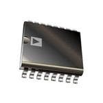
| 产品图片 |
|
| rohs | 符合RoHS无铅 / 符合限制有害物质指令(RoHS)规范要求 |
| 产品系列 | 数字电位计 IC,Analog Devices AD5142ABRUZ100- |
| 数据手册 | |
| 产品型号 | AD5142ABRUZ100 |
| POT数量 | Dual |
| 产品种类 | 数字电位计 IC |
| 供应商器件封装 | 16-TSSOP |
| 包装 | 管件 |
| 商标 | Analog Devices |
| 存储器类型 | 非易失 |
| 安装类型 | 表面贴装 |
| 安装风格 | SMD/SMT |
| 容差 | 8 % |
| 封装 | Tube |
| 封装/外壳 | 16-TSSOP(0.173",4.40mm 宽) |
| 封装/箱体 | TSSOP-16 |
| 工作温度 | -40°C ~ 125°C |
| 工作电源电压 | 5.5 V |
| 工厂包装数量 | 96 |
| 弧刷存储器 | Non Volatile |
| 抽头 | 256 |
| 接口 | I²C(设备位址) |
| 数字接口 | I2C |
| 最大工作温度 | + 125 C |
| 最小工作温度 | - 40 C |
| 标准包装 | 96 |
| 每POT分接头 | 256 |
| 温度系数 | 35 PPM / C |
| 电压-电源 | 2.3 V ~ 5.5 V, ±2.25 V ~ 2.75 V |
| 电源电压-最大 | 5.5 V |
| 电源电压-最小 | 2.3 V |
| 电源电流 | 700 nA |
| 电路数 | 2 |
| 电阻 | 100 kOhms |
| 电阻(Ω) | 100k |
| 系列 | AD5142A |
| 视频文件 | http://www.digikey.cn/classic/video.aspx?PlayerID=1364138032001&width=640&height=505&videoID=2182927010001http://www.digikey.cn/classic/video.aspx?PlayerID=1364138032001&width=640&height=505&videoID=2585547407001 |


- 商务部:美国ITC正式对集成电路等产品启动337调查
- 曝三星4nm工艺存在良率问题 高通将骁龙8 Gen1或转产台积电
- 太阳诱电将投资9.5亿元在常州建新厂生产MLCC 预计2023年完工
- 英特尔发布欧洲新工厂建设计划 深化IDM 2.0 战略
- 台积电先进制程称霸业界 有大客户加持明年业绩稳了
- 达到5530亿美元!SIA预计今年全球半导体销售额将创下新高
- 英特尔拟将自动驾驶子公司Mobileye上市 估值或超500亿美元
- 三星加码芯片和SET,合并消费电子和移动部门,撤换高东真等 CEO
- 三星电子宣布重大人事变动 还合并消费电子和移动部门
- 海关总署:前11个月进口集成电路产品价值2.52万亿元 增长14.8%


PDF Datasheet 数据手册内容提取
Dual Channel, 128-/256-Position, I2C, Nonvolatile Digital Potentiometer Data Sheet AD5122A/AD5142A FEATURES FUNCTIONAL BLOCK DIAGRAM 10 kΩ and 100 kΩ resistance options VLOGIC VDD INDEP Resistor tolerance: 8% maximum POWER-ON Wiper current: ±6 mA RESET AD5122A/ AD5142A Low temperature coefficient: 35 ppm/°C Wide bandwidth: 3 MHz RDAC1 A1 Fast start-up time < 75 µs RESET INPUT W1 Linear gain setting mode REGISTER 1 SCL B1 Single- and dual-supply operation SERIAL RDAC2 Independent logic supply: 1.8 V to 5.5 V SDA INTERFACE 7/8 INPUT A2 REGISTER 2 W2 Wide operating temperature: −40°C to +125°C ADDR1 B2 3 mm × 3 mm package option ADDR0 EEPROM MEMORY Qualified for automotive applications APoPrPtaLbIlCe AelTeIcOtrNonSic s level adjustment GND VSS 10939-001 LCD panel brightness and contrast controls Figure 1. Programmable filters, delays, and time constants Programmable power supplies GENERAL DESCRIPTION The AD5122A/AD5142A potentiometers provide a nonvolatile Table 1. Family Models solution for 128-/256-position adjustment applications, offering Model Channel Position Interface Package guaranteed low resistor tolerance errors of ±8% and up to ±6 mA AD51231 Quad 128 I2C LFCSP current density in the Ax, Bx, and Wx pins. AD5124 Quad 128 SPI/I2C LFCSP The low resistor tolerance and low nominal temperature coefficient AD5124 Quad 128 SPI TSSOP simplify open-loop applications as well as applications requiring AD51431 Quad 256 I2C LFCSP tolerance matching. AD5144 Quad 256 SPI/I2C LFCSP AD5144 Quad 256 SPI TSSOP The linear gain setting mode allows independent programming AD5144A Quad 256 I2C TSSOP of the resistance between the digital potentiometer terminals, through R and R the string resistors, allowing very accurate AD5122 Dual 128 SPI LFCSP/TSSOP AW WB resistor matching. AD5122A Dual 128 I2C LFCSP/TSSOP AD5142 Dual 256 SPI LFCSP/TSSOP The high bandwidth and low total harmonic distortion (THD) AD5142A Dual 256 I2C LFCSP/TSSOP ensure optimal performance for ac signals, making it suitable AD5121 Single 128 SPI/I2C LFCSP for filter design. AD5141 Single 256 SPI/I2C LFCSP The low wiper resistance of only 40 Ω at the ends of the resistor 1 Two potentiometers and two rheostats. array allows for pin-to-pin connection. The wiper values can be set through an I2C-compatible digital interface that is also used to read back the wiper register and EEPROM contents. The AD5122A/AD5142A are available in a compact, 16-lead, 3 mm × 3 mm LFCSP and a 16-lead TSSOP. The parts are guaranteed to operate over the extended industrial temperature range of −40°C to +125°C. Rev. B Document Feedback Information furnished by Analog Devices is believed to be accurate and reliable. However, no responsibility is assumed by Analog Devices for its use, nor for any infringements of patents or other One Technology Way, P.O. Box 9106, Norwood, MA 02062-9106, U.S.A. rights of third parties that may result from its use. Specifications subject to change without notice. No license is granted by implication or otherwise under any patent or patent rights of Analog Devices. Tel: 781.329.4700 ©2012–2017 Analog Devices, Inc. All rights reserved. Trademarks and registered trademarks are the property of their respective owners. Technical Support www.analog.com
AD5122A/AD5142A Data Sheet TABLE OF CONTENTS Features .............................................................................................. 1 RDAC Register and EEPROM .................................................. 20 Applications ....................................................................................... 1 Input Shift Register .................................................................... 20 Functional Block Diagram .............................................................. 1 I2C Serial Data Interface ............................................................ 20 General Description ......................................................................... 1 I2C Address .................................................................................. 20 Revision History ............................................................................... 2 Advanced Control Modes ......................................................... 22 Specifications ..................................................................................... 3 EEPROM or RDAC Register Protection ................................. 23 Electrical Characteristics—AD5122A ....................................... 3 INDEP Pin ................................................................................... 23 Electrical Characteristics—AD5142A ....................................... 6 RDAC Architecture .................................................................... 26 Interface Timing Specifications .................................................. 9 Programming the Variable Resistor ......................................... 26 Shift Register and Timing Diagrams ....................................... 10 Programming the Potentiometer Divider ............................... 27 Absolute Maximum Ratings .......................................................... 11 Terminal Voltage Operating Range ......................................... 27 Thermal Resistance .................................................................... 11 Power-Up Sequence ................................................................... 27 ESD Caution ................................................................................ 11 Layout and Power Supply Biasing ............................................ 27 Pin Configurations and Function Descriptions ......................... 12 Outline Dimensions ....................................................................... 28 Typical Performance Characteristics ........................................... 14 Ordering Guide .......................................................................... 29 Test Circuits ..................................................................................... 19 Automotive Products ................................................................. 29 Theory of Operation ...................................................................... 20 REVISION HISTORY 6/2017—Rev. A to Rev. B Changes to Figure 18 ...................................................................... 16 Changes to Features Section............................................................ 1 Change to Linear Gain Setting Mode .......................................... 22 Changes to Logic Supply Current Parameter, Table 2 ................. 4 Changes to EEPROM or RDAC Register Protection Section ... 23 Added Note 12 to Data Retention Parameter, Table 2; Changes to RDAC Architecture Section ..................................... 26 Renumbered Sequentially ................................................................ 5 Updated Outline Dimensions ....................................................... 28 Changes to Logic Supply Current Parameter, Table 3 ................. 7 Changes to Ordering Guide .......................................................... 29 Added Note 12 to Data Retention Parameter, Table 3; Added Automotive Products Section .......................................... 29 Renumbered Sequentially ................................................................ 8 Changes to Table 5 .......................................................................... 11 12/2012—Rev. 0 to Rev. A Changes to Figure 4 and Table 7 ................................................... 12 Changes to Table 9 .......................................................................... 20 Changes to Figure 14 ...................................................................... 15 Added Figure 15; Renumbered Sequentially .............................. 15 10/2012—Revision 0: Initial Version Rev. B | Page 2 of 32
Data Sheet AD5122A/AD5142A SPECIFICATIONS ELECTRICAL CHARACTERISTICS—AD5122A V = 2.3 V to 5.5 V, V = 0 V; V = 2.25 V to 2.75 V, V = −2.25 V to −2.75 V; V = 1.8 V to 5.5 V, −40°C < T < +125°C, unless DD SS DD SS LOGIC A otherwise noted. Table 2. Parameter Symbol Test Conditions/Comments Min Typ1 Max Unit DC CHARACTERISTICS—RHEOSTAT MODE (ALL RDACs) Resolution N 7 Bits Resistor Integral Nonlinearity2 R-INL R = 10 kΩ AB V ≥ 2.7 V −1 ±0.1 +1 LSB DD V < 2.7 V −2.5 ±1 +2.5 LSB DD R = 100 kΩ AB V ≥ 2.7 V −0.5 ±0.1 +0.5 LSB DD V < 2.7 V −1 ±0.25 +1 LSB DD Resistor Differential Nonlinearity2 R-DNL −0.5 ±0.1 +0.5 LSB Nominal Resistor Tolerance ΔR /R −8 ±1 +8 % AB AB Resistance Temperature Coefficient3 (ΔR /R )/ΔT × 106 Code = full scale 35 ppm/°C AB AB Wiper Resistance3 R Code = zero scale W R = 10 kΩ 55 125 Ω AB R = 100 kΩ 130 400 Ω AB Bottom Scale or Top Scale R or R BS TS R = 10 kΩ 40 80 Ω AB R = 100 kΩ 60 230 Ω AB Nominal Resistance Match R /R Code = 0xFF −1 ±0.2 +1 % AB1 AB2 DC CHARACTERISTICS—POTENTIOMETER DIVIDER MODE (ALL RDACs) Integral Nonlinearity4 INL R = 10 kΩ −0.5 ±0.1 +0.5 LSB AB R = 100 kΩ −0.25 ±0.1 +0.25 LSB AB Differential Nonlinearity4 DNL −0.25 ±0.1 +0.25 LSB Full-Scale Error V WFSE R = 10 kΩ −1.5 −0.1 LSB AB R = 100 kΩ −0.5 ±0.1 +0.5 LSB AB Zero-Scale Error V WZSE R = 10 kΩ 1 1.5 LSB AB R = 100 kΩ 0.25 0.5 LSB AB Voltage Divider Temperature (ΔV /V )/ΔT × 106 Code = half scale ±5 ppm/°C W W Coefficient3 Rev. B | Page 3 of 32
AD5122A/AD5142A Data Sheet Parameter Symbol Test Conditions/Comments Min Typ1 Max Unit RESISTOR TERMINALS Maximum Continuous Current I , I , and I A B W R = 10 kΩ −6 +6 mA AB R = 100 kΩ −1.5 +1.5 mA AB Terminal Voltage Range5 V V V SS DD Capacitance A, Capacitance B3 C , C f = 1 MHz, measured to GND, A B code = half scale R = 10 kΩ 25 pF AB R = 100 kΩ 12 pF AB Capacitance W3 C f = 1 MHz, measured to GND, W code = half scale R = 10 kΩ 12 pF AB R = 100 kΩ 5 pF AB Common-Mode Leakage Current3 V = V = V −500 ±15 +500 nA A W B DIGITAL INPUTS Input Logic3 High V V = 1.8 V to 2.3 V 0.8 × V V INH LOGIC LOGIC V = 2.3 V to 5.5 V 0.7 × V V LOGIC LOGIC Low V 0.2 × V V INL LOGIC Input Hysteresis3 V 0.1 × V V HYST LOGIC Input Current3 I ±1 µA IN Input Capacitance3 C 5 pF IN DIGITAL OUTPUTS Output High Voltage3 V R = 2.2 kΩ to V V V OH PULL-UP LOGIC LOGIC Output Low Voltage3 V I = 3 mA 0.4 V OL SINK I = 6 mA, V > 2.3 V 0.6 V SINK LOGIC Three-State Leakage Current −1 +1 µA Three-State Output Capacitance 2 pF POWER SUPPLIES Single-Supply Power Range V = GND 2.3 5.5 V SS Dual-Supply Power Range ±2.25 ±2.75 V Logic Supply Range Single supply, V = GND 1.8 V V SS DD Dual supply, V < GND 2.25 V V SS DD Positive Supply Current I V = V or V = GND DD IH LOGIC IL V = 5.5 V 0.7 5.5 µA DD V = 2.3 V 400 nA DD Negative Supply Current I V = V or V = GND −5.5 −0.7 µA SS IH LOGIC IL EEPROM Store Current3, 6 I V = V or V = GND 2 mA DD_EEPROM_STORE IH LOGIC IL EEPROM Read Current3, 7 I V = V or V = GND 320 µA DD_EEPROM_READ IH LOGIC IL Logic Supply Current I V = V or V = GND 0.05 1.4 µA LOGIC IH LOGIC IL Power Dissipation8 P V = V or V = GND 3.5 µW DISS IH LOGIC IL Power Supply Rejection Ratio PSRR ∆V /∆V = V ± 10%, −66 −60 dB DD SS DD code = full scale Rev. B | Page 4 of 32
Data Sheet AD5122A/AD5142A Parameter Symbol Test Conditions/Comments Min Typ1 Max Unit DYNAMIC CHARACTERISTICS9 Bandwidth BW −3 dB R = 10 kΩ 3 MHz AB R = 100 kΩ 0.43 MHz AB Total Harmonic Distortion THD V /V = ±2.5 V, V = 1 V rms, DD SS A V = 0 V, f = 1 kHz B R = 10 kΩ −80 dB AB R = 100 kΩ −90 dB AB Resistor Noise Density e Code = half scale, T = 25°C, N_WB A f = 10 kHz R = 10 kΩ 7 nV/√Hz AB R = 100 kΩ 20 nV/√Hz AB V Settling Time t V = 5 V, V = 0 V, from W S A B zero scale to full scale, ±0.5 LSB error band R = 10 kΩ 2 µs AB R = 100 kΩ 12 µs AB Crosstalk (C /C ) C R = 10 kΩ 10 nV-sec W1 W2 T AB R = 100 kΩ 25 nV-sec AB Analog Crosstalk C −90 dB TA Endurance10 T = 25°C 1 Mcycles A 100 kcycles Data Retention11, 12 50 Years 1 Typical values represent average readings at 25°C, V = 5 V, V = 0 V, and V = 5 V. DD SS LOGIC 2 Resistor integral nonlinearity (R-INL) error is the deviation from an ideal value measured between the maximum resistance and the minimum resistance wiper positions. R-DNL measures the relative step change from ideal between successive tap positions. The maximum wiper current is limited to (0.7 × V )/R . DD AB 3 Guaranteed by design and characterization, not subject to production test. 4 INL and DNL are measured at V with the RDAC configured as a potentiometer divider similar to a voltage output DAC. V = V and V = 0 V. DNL specification limits WB A DD B of ±1 LSB maximum are guaranteed monotonic operating conditions. 5 Resistor Terminal A, Resistor Terminal B, and Resistor Terminal W have no limitations on polarity with respect to each other. Dual-supply operation enables ground referenced bipolar signal adjustment. 6 Different from operating current; supply current for EEPROM program lasts approximately 30 ms. 7 Different from operating current; supply current for EEPROM read lasts approximately 20 µs. 8 P is calculated from (I × V ) + (I × V ). DISS DD DD LOGIC LOGIC 9 All dynamic characteristics use V /V = ±2.5 V, and V = 2.5 V. DD SS LOGIC 10 Endurance is qualified to 100,000 cycles per JEDEC Standard 22, Method A117 and measured at −40°C to +125°C. 11 Retention lifetime equivalent at junction temperature (TJ) = 125°C per JEDEC Standard 22, Method A117. Retention lifetime, based on an activation energy of 1 eV, derates with junction temperature in the Flash/EE memory. 12 50 years apply to an endurance of 1000 cycles. An endurance of 100,000 cycles has an equivalent retention lifetime of 5 years. Rev. B | Page 5 of 32
AD5122A/AD5142A Data Sheet ELECTRICAL CHARACTERISTICS—AD5142A V = 2.3 V to 5.5 V, V = 0 V; V = 2.25 V to 2.75 V, V = −2.25 V to −2.75 V; V = 1.8 V to 5.5 V, −40°C < T < +125°C, unless DD SS DD SS LOGIC A otherwise noted. Table 3. Parameter Symbol Test Conditions/Comments Min Typ1 Max Unit DC CHARACTERISTICS—RHEOSTAT MODE (ALL RDACs) Resolution N 8 Bits Resistor Integral Nonlinearity2 R-INL R = 10 kΩ AB V ≥ 2.7 V −2 ±0.2 +2 LSB DD V < 2.7 V −5 ±1.5 +5 LSB DD R = 100 kΩ AB V ≥ 2.7 V −1 ±0.1 +1 LSB DD V < 2.7 V −2 ±0.5 +2 LSB DD Resistor Differential Nonlinearity2 R-DNL −0.5 ±0.2 +0.5 LSB Nominal Resistor Tolerance ΔR /R −8 ±1 +8 % AB AB Resistance Temperature Coefficient3 (ΔR /R )/ΔT × 106 Code = full scale 35 ppm/°C AB AB Wiper Resistance3 R Code = zero scale W R = 10 kΩ 55 125 Ω AB R = 100 kΩ 130 400 Ω AB Bottom Scale or Top Scale R or R BS TS R = 10 kΩ 40 80 Ω AB R = 100 kΩ 60 230 Ω AB Nominal Resistance Match R /R Code = 0xFF −1 ±0.2 +1 % AB1 AB2 DC CHARACTERISTICS—POTENTIOMETER DIVIDER MODE (ALL RDACs) Integral Nonlinearity4 INL R = 10 kΩ −1 ±0.2 +1 LSB AB R = 100 kΩ −0.5 ±0.1 +0.5 LSB AB Differential Nonlinearity4 DNL −0.5 ±0.2 +0.5 LSB Full-Scale Error V WFSE R = 10 kΩ −2.5 −0.1 LSB AB R = 100 kΩ −1 ±0.2 +1 LSB AB Zero-Scale Error V WZSE R = 10 kΩ 1.2 3 LSB AB R = 100 kΩ 0.5 1 LSB AB Voltage Divider Temperature (ΔV /V )/ΔT × 106 Code = half scale ±5 ppm/°C W W Coefficient3 Rev. B | Page 6 of 32
Data Sheet AD5122A/AD5142A Parameter Symbol Test Conditions/Comments Min Typ1 Max Unit RESISTOR TERMINALS Maximum Continuous Current I , I , and I A B W R = 10 kΩ −6 +6 mA AB R = 100 kΩ −1.5 +1.5 mA AB Terminal Voltage Range5 V V V SS DD Capacitance A, Capacitance B3 C , C f = 1 MHz, measured to GND, A B code = half scale R = 10 kΩ 25 pF AB R = 100 kΩ 12 pF AB Capacitance W3 C f = 1 MHz, measured to GND, W code = half scale R = 10 kΩ 12 pF AB R = 100 kΩ 5 pF AB Common-Mode Leakage Current3 V = V = V −500 ±15 +500 nA A W B DIGITAL INPUTS Input Logic3 High V V = 1.8 V to 2.3 V 0.8 × V V INH LOGIC LOGIC V = 2.3 V to 5.5 V 0.7 × V V LOGIC LOGIC Low V 0.2 × V V INL LOGIC Input Hysteresis3 V 0.1 × V V HYST LOGIC Input Current3 I ±1 µA IN Input Capacitance3 C 5 pF IN DIGITAL OUTPUTS Output High Voltage3 V R = 2.2 kΩ to V V V OH PULL-UP LOGIC LOGIC Output Low Voltage3 V I = 3 mA 0.4 V OL SINK I = 6 mA, V > 2.3 V 0.6 V SINK LOGIC Three-State Leakage Current −1 +1 µA Three-State Output Capacitance 2 pF POWER SUPPLIES Single-Supply Power Range V = GND 2.3 5.5 V SS Dual-Supply Power Range ±2.25 ±2.75 V Logic Supply Range Single supply, V = GND 1.8 V V SS DD Dual supply, V < GND 2.25 V V SS DD Positive Supply Current I V = V or V = GND DD IH LOGIC IL V = 5.5 V 0.7 5.5 µA DD V = 2.3 V 400 nA DD Negative Supply Current I V = V or V = GND −5.5 −0.7 µA SS IH LOGIC IL EEPROM Store Current3, 6 I V = V or V = GND 2 mA DD_EEPROM_STORE IH LOGIC IL EEPROM Read Current3, 7 I V = V or V = GND 320 µA DD_EEPROM_READ IH LOGIC IL Logic Supply Current I V = V or V = GND 0.05 1.4 µA LOGIC IH LOGIC IL Power Dissipation8 P V = V or V = GND 3.5 µW DISS IH LOGIC IL Power Supply Rejection Ratio PSR ∆V /∆V = V ± 10%, −66 −60 dB DD SS DD code = full scale Rev. B | Page 7 of 32
AD5122A/AD5142A Data Sheet Parameter Symbol Test Conditions/Comments Min Typ1 Max Unit DYNAMIC CHARACTERISTICS9 Bandwidth BW −3 dB R = 10 kΩ 3 MHz AB R = 100 kΩ 0.43 MHz AB Total Harmonic Distortion THD V /V = ±2.5 V, V = 1 V rms, DD SS A V = 0 V, f = 1 kHz B R = 10 kΩ −80 dB AB R = 100 kΩ −90 dB AB Resistor Noise Density e Code = half scale, T = 25°C, N_WB A f = 10 kHz R = 10 kΩ 7 nV/√Hz AB R = 100 kΩ 20 nV/√Hz AB V Settling Time t V = 5 V, V = 0 V, from W S A B zero scale to full scale, ±0.5 LSB error band R = 10 kΩ 2 µs AB R = 100 kΩ 12 µs AB Crosstalk (C /C ) C R = 10 kΩ 10 nV-sec W1 W2 T AB R = 100 kΩ 25 nV-sec AB Analog Crosstalk C −90 dB TA Endurance10 T = 25°C 1 Mcycles A 100 kcycles Data Retention11, 12 50 Years 1 Typical values represent average readings at 25°C, V = 5 V, V = 0 V, and V = 5 V. DD SS LOGIC 2 Resistor integral nonlinearity (R-INL) error is the deviation from an ideal value measured between the maximum resistance and the minimum resistance wiper positions. R-DNL measures the relative step change from ideal between successive tap positions. The maximum wiper current is limited to (0.7 × V )/R . DD AB 3 Guaranteed by design and characterization, not subject to production test. 4 INL and DNL are measured at V with the RDAC configured as a potentiometer divider similar to a voltage output DAC. V = V and V = 0 V. DNL specification limits WB A DD B of ±1 LSB maximum are guaranteed monotonic operating conditions. 5 Resistor Terminal A, Resistor Terminal B, and Resistor Terminal W have no limitations on polarity with respect to each other. Dual-supply operation enables ground referenced bipolar signal adjustment. 6 Different from operating current; supply current for EEPROM program lasts approximately 30 ms. 7 Different from operating current; supply current for EEPROM read lasts approximately 20 µs. 8 P is calculated from (I × V ) + (I × V ). DISS DD DD LOGIC LOGIC 9 All dynamic characteristics use V /V = ±2.5 V, and V = 2.5 V. DD SS LOGIC 10 Endurance is qualified to 100,000 cycles per JEDEC Standard 22, Method A117 and measured at −40°C to +125°C. 11 Retention lifetime equivalent at junction temperature (TJ) = 125°C per JEDEC Standard 22, Method A117. Retention lifetime, based on an activation energy of 1 eV, derates with junction temperature in the Flash/EE memory. 12 50 years apply to an endurance of 1000 cycles. An endurance of 100,000 cycles has an equivalent retention lifetime of 5 years. Rev. B | Page 8 of 32
Data Sheet AD5122A/AD5142A INTERFACE TIMING SPECIFICATIONS V = 1.8 V to 5.5 V; all specifications T to T , unless otherwise noted. LOGIC MIN MAX Table 4. Parameter1 Test Conditions/Comments Min Typ Max Unit Description f 2 Standard mode 100 kHz Serial clock frequency SCL Fast mode 400 kHz t Standard mode 4.0 µs SCL high time, t 1 HIGH Fast mode 0.6 µs t Standard mode 4.7 µs SCL low time, t 2 LOW Fast mode 1.3 µs t Standard mode 250 ns Data setup time, t 3 SU; DAT Fast mode 100 ns t Standard mode 0 3.45 µs Data hold time, t 4 HD; DAT Fast mode 0 0.9 µs t Standard mode 4.7 µs Setup time for a repeated start condition, t 5 SU; STA Fast mode 0.6 µs t Standard mode 4 µs Hold time (repeated) for a start condition, t 6 HD; STA Fast mode 0.6 µs t Standard mode 4.7 µs Bus free time between a stop and a start condition, t 7 BUF Fast mode 1.3 µs t Standard mode 4 µs Setup time for a stop condition, t 8 SU; STO Fast mode 0.6 µs t Standard mode 1000 ns Rise time of SDA signal, t 9 RDA Fast mode 20 + 0.1 C 300 ns L t Standard mode 300 ns Fall time of SDA signal, t 10 FDA Fast mode 20 + 0.1 C 300 ns L t Standard mode 1000 ns Rise time of SCL signal, t 11 RCL Fast mode 20 + 0.1 C 300 ns L t Standard mode 1000 ns Rise time of SCL signal after a repeated start condition 11A and after an acknowledge bit, t (not shown in Figure 3) RCL1 Fast mode 20 + 0.1 C 300 ns L t Standard mode 300 ns Fall time of SCL signal, t 12 FCL Fast mode 20 + 0.1 C 300 ns L t 3 Fast mode 0 50 ns Pulse width of suppressed spike (not shown in Figure 3) SP t 0.1 10 µs RESET low time (not shown in Figure 3) RESET t 4 15 50 ms Memory program time (not shown in Figure 3) EEPROM_PROGRAM t 7 30 µs Memory readback time (not shown in Figure 3) EEPROM_READBACK t 5 75 µs Power-on EEPROM restore time (not shown in Figure 3) POWER_UP t 30 µs Reset EEPROM restore time (not shown in Figure 3) RESET 1 Maximum bus capacitance is limited to 400 pF. 2 The SDA and SCL timing is measured with the input filters enabled. Switching off the input filters improves the transfer rate; however, it has a negative effect on the EMC behavior of the part. 3 Input filtering on the SCL and SDA inputs suppresses noise spikes that are less than 50 ns for fast mode. 4 The EEPROM program time depends on the temperature and EEPROM write cycles. Higher timing is expected at lower temperatures and higher write cycles. 5 Maximum time after V − V is equal to 2.3 V. DD SS Rev. B | Page 9 of 32
AD5122A/AD5142A Data Sheet SHIFT REGISTER AND TIMING DIAGRAMS DB15 (MSB) DB8 DB7 DB0 (LSB) C3 C2 C1 C0 A3 A2 A1 A0 D7 D6 D5 D4 D3 D2 D1 D0 CONTROL BITS ADDRESS BITS DATA BITS 10939-002 Figure 2. Input Shift Register Contents t11 t12 t6 t8 t 2 SCL t6 t4 t1 t3 t5 t10 t9 SDA P t7 S S P 10939-003 Figure 3. I2C Serial Interface Timing Diagram (Typical Write Sequence) Rev. B | Page 10 of 32
Data Sheet AD5122A/AD5142A ABSOLUTE MAXIMUM RATINGS T = 25°C, unless otherwise noted. Stresses at or above those listed under Absolute Maximum A Ratings may cause permanent damage to the product. This is a Table 5. stress rating only; functional operation of the product at these Parameter Rating or any other conditions above those indicated in the operational V to GND −0.3 V to +7.0 V DD section of this specification is not implied. Operation beyond V to GND +0.3 V to −7.0 V SS the maximum operating conditions for extended periods may V to V 7 V DD SS affect product reliability. V to GND −0.3 V to V + 0.3 V or LOGIC DD THERMAL RESISTANCE +7.0 V (whichever is less) V , V , V to GND V − 0.3 V, V + 0.3 V θ is defined by the JEDEC JESD51 standard, and the value is A W B SS DD JA +7.0 V (whichever is less) dependent on the test board and test environment. I , I , I A W B Pulsed1 Table 6. Thermal Resistance Frequency > 10 kHz Package Type θ θ Unit JA JC R = 10 kΩ ±6 mA/d2 16-Lead LFCSP 89.51 3 °C/W AW R = 100 kΩ ±1.5 mA/d2 16-Lead TSSOP 150.41 27.6 °C/W AW Frequency ≤ 10 kHz 1 JEDEC 2S2P test board, still air (0 m/sec airflow). R = 10 kΩ ±6 mA/√d2 AW R = 100 kΩ ±1.5 mA/√d2 AW Digital Inputs −0.3 V to V + 0.3 V or ESD CAUTION LOGIC +7 V (whichever is less) Operating Temperature Range, T 3 −40°C to +125°C A Maximum Junction Temperature, 150°C T Maximum J Storage Temperature Range −65°C to +150°C Reflow Soldering Peak Temperature 260°C Time at Peak Temperature 20 sec to 40 sec Package Power Dissipation (T max − T )/θ J A JA FICDM 1.5 kV 1 Maximum terminal current is bounded by the maximum current handling of the switches, maximum power dissipation of the package, and maximum applied voltage across any two of the A, B, and W terminals at a given resistance. 2 d = pulse duty factor. 3 Includes programming of EEPROM memory. Rev. B | Page 11 of 32
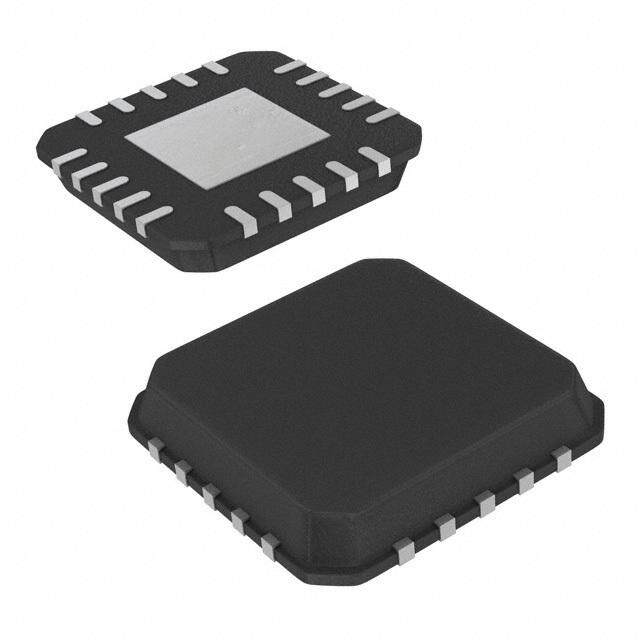
AD5122A/AD5142A Data Sheet PIN CONFIGURATIONS AND FUNCTION DESCRIPTIONS PIN 1 TESER INDEP 0RDDA ADDR1 INDICATOR 61 51 41 31 GND1 12 SDA AD5122A/ A12 AD5142A 11 SCL W13 TOP VIEW 10 VLOGIC B14 (Not to Scale) 9 VDD 5 6 7 8 S 2 2 2 S A W B V NOTES 1.EXPOSED PAD. CONNECT THE EXPOSED PAD TO THE POTENTIAL OF THE VSS PIN, OR, ALTERNATIVELY, LEAVE IT ETFHOLEERC PETANRDHIC ABANELC LTEYHD EU TRNHMCEAORLNMLNYAE LCC POTEENRDNF.E OICTRT IMESD AR NTECOCEO A.M CMOEPNPDEERD P TLHAANTE 10939-004 Figure 4. 16-Lead LFCSP Pin Configuration Table 7. 16-Lead LFCSP Pin Function Descriptions Pin No. Mnemonic Description 1 GND Ground Pin, Logic Ground Reference. 2 A1 Terminal A of RDAC1. V ≤ V ≤ V . SS A DD 3 W1 Wiper Terminal of RDAC1. V ≤ V ≤ V . SS W DD 4 B1 Terminal B of RDAC1. V ≤ V ≤ V . SS B DD 5 V Negative Power Supply. Decouple this pin with 0.1 μF ceramic capacitors and 10 μF capacitors. SS 6 A2 Terminal A of RDAC2. V ≤ V ≤ V . SS A DD 7 W2 Wiper Terminal of RDAC2. V ≤ V ≤ V . SS W DD 8 B2 Terminal B of RDAC2. V ≤ V ≤ V . SS B DD 9 V Positive Power Supply. Decouple this pin with 0.1 μF ceramic capacitors and 10 μF capacitors. DD 10 V Logic Power Supply; 1.8 V to V . Decouple this pin with 0.1 μF ceramic capacitors and 10 μF capacitors. LOGIC DD 11 SCL Serial Clock Line. 12 SDA Serial Data Input/Output. 13 ADDR1 Programmable Address (ADDR1) for Multiple Package Decoding. 14 ADDR0 Programmable Address (ADDR0) for Multiple Package Decoding. 15 INDEP Linear Gain Setting Mode at Power-Up. Each string resistor is loaded from its associated memory location. If INDEP is enabled, it cannot be disabled by the software. 16 RESET Hardware Reset Pin. Refresh the RDAC registers from EEPROM. RESET is activated at logic low. If this pin is not used, tie RESET to V . LOGIC EPAD Exposed Pad. Connect this exposed pad to the potential of the V pin, or, alternatively, leave it electrically SS unconnected. It is recommended that the pad be thermally connected to a copper plane for enhanced thermal performance. Rev. B | Page 12 of 32
Data Sheet AD5122A/AD5142A INDEP 1 16 ADDR0 RESET 2 15 ADDR1 GND 3 14 SDA AD5122A/ A1 4 AD5142A 13 SCL W1 5 TOP VIEW 12 VLOGIC (Not to Scale) B1 6 11 VDD VSS 7 10 B2 A2 8 9 W2 10939-005 Figure 5. 16-Lead TSSOP Pin Configuration Table 8. 16-Lead TSSOP Pin Function Descriptions Pin No. Mnemonic Description 1 INDEP Linear Gain Setting Mode at Power-Up. Each string resistor is loaded from its associated memory location. If INDEP is enabled, it cannot be disabled by the software. 2 RESET Hardware Reset Pin. Refresh the RDAC registers from EEPROM. RESET is activated at logic low. If this pin is not used, tie RESET to V . LOGIC 3 GND Ground Pin, Logic Ground Reference. 4 A1 Terminal A of RDAC1. V ≤ V ≤ V . SS A DD 5 W1 Wiper Terminal of RDAC1. V ≤ V ≤ V . SS W DD 6 B1 Terminal B of RDAC1. V ≤ V ≤ V . SS B DD 7 V Negative Power Supply. Decouple this pin with 0.1 µF ceramic capacitors and 10 µF capacitors. SS 8 A2 Terminal A of RDAC2. V ≤ V ≤ V . SS A DD 9 W2 Wiper Terminal of RDAC2. V ≤ V ≤ V . SS W DD 10 B2 Terminal B of RDAC2. V ≤ V ≤ V . SS B DD 11 V Positive Power Supply. Decouple this pin with 0.1 µF ceramic capacitors and 10 µF capacitors. DD 12 V Logic Power Supply; 1.8 V to V . Decouple this pin with 0.1 µF ceramic capacitors and 10 µF capacitors. LOGIC DD 13 SCL Serial Clock Line. 14 SDA Serial Data Input/Output. 15 ADDR1 Programmable Address (ADDR1) for Multiple Package Decoding. 16 ADDR0 Programmable Address (ADDR0) for Multiple Package Decoding. Rev. B | Page 13 of 32
AD5122A/AD5142A Data Sheet TYPICAL PERFORMANCE CHARACTERISTICS 0.5 0.2 10kΩ,+125°C 0.4 10kΩ, +25°C 10kΩ,–40°C 0.1 100kΩ, +125°C 0.3 100kΩ, +25°C 100kΩ, –40°C 0 0.2 B) 0.1 B)–0.1 S S NL (L 0 NL (L–0.2 R-I–0.1 R-D–0.3 –0.2 –0.4 –0.3 –0.5 –0.4 10kΩ,+125°C 100kΩ,+125°C 10kΩ,+25°C 100kΩ,+25°C 10kΩ,–40°C 100kΩ,–40°C –0.50 C10O0DE (Decimal) 200 10939-006 –0.60 1C0O0DE (Decimal) 200 10939-009 Figure 6. R-INL vs. Code (AD5142A) Figure 9. R-DNL vs. Code (AD5142A) 0.20 0.10 0.15 0.05 0.10 0 0.05 B) B) –0.05 R-INL (LS –0.050 R-DNL (LS ––00..1150 –0.10 10kΩ,+125°C –0.20 –0.15 10kΩ,+25°C 10kΩ,–40°C –0.20 110000kkΩΩ,,++12255°C°C –0.25 1100kkΩΩ,,++12255°C°C 110000kkΩΩ,,++12255°C°C 100kΩ,–40°C 10kΩ,–40°C 100kΩ,–40°C –0.25 0 C5O0DE (Decimal) 100 10939-007 –0.300 C50ODE (Decimal) 100 10939-010 Figure 7. R-INL vs. Code (AD5122A) Figure 10. R-DNL vs. Code (AD5122A) 0.3 0.10 10kΩ, –40°C 10kΩ, +25°C 10kΩ, +125°C 0.05 0.2 100kΩ, –40°C 100kΩ, +25°C 100kΩ, +125°C 0 0.1 –0.05 B) B) NL(LS 0 NL(LS–0.10 I D –0.15 –0.1 –0.20 –0.2 –0.25 10kΩ,–40°C 100kΩ,–40°C 10kΩ,+25°C 100kΩ,+25°C 10kΩ,+125°C 100kΩ,+125°C –0.30 C10O0DE(Decimal) 200 10939-008 –0.300 C10O0DE(Decimal) 200 10939-011 Figure 8. INL vs. Code (AD5142A) Figure 11. DNL vs. Code (AD5142A) Rev. B | Page 14 of 32
Data Sheet AD5122A/AD5142A 0.15 1000 111000kkkΩΩΩ,,, –++421025°5°CC°C 900 VVDSSD == GVLNODGIC VVLLOOGGIICC == 23..33VV 0.10 100kΩ,–40°C VLOGIC = 5.5V 100kΩ, +25°C 800 100kΩ, +125°C 700 0.05 L (LSB) 0 (nA)GIC 560000 N O I IL 400 –0.05 300 200 –0.10 100 –0.15 0 0 C50ODE (Decimal) 100 10939-012 –40 –20 0 T2E0MPERA40TURE (6°0C) 80 100 120 10939-160 Figure 12. INL vs. Code (AD5122A) Figure 15. ILOGIC vs. Temperature 450 0.06 100kΩ 10kΩ, –40°C 100kΩ, –40°C 10kΩ 10kΩ, +25°C 100kΩ, +25°C E 400 0.04 10kΩ, +125°C 100kΩ, +125°C R U AT 350 0.02 R PEC) 300 0 EMm/° R MODE TCIENT (pp 220500 NL (LSB) ––00..0042 ETEEFFI 150 D –0.06 OMCO 100 –0.08 TI EN 50 –0.10 T O P 0 –0.12 –50 00 5205 C15O000DE (Decim175a50l) 210000 215257 AADD55112422AA 10939-013 –0.140 Figure 16. DNC5L0O vDsE. C(Doedceim (AalD)5122A) 100 10939-015 Figure 13. Potentiometer Mode Temperature Coefficient ((ΔVW/VW)/ΔT × 106) vs. Code 450 10kΩ 800 100kΩ VDD = VLOGIC 400 700 VSS = GND RE 350 U T 600 PERAm/°C)300 500 TEMT(pp250 I (nA)DD 400 ATMODEEFFICIEN125000 300 STCO100 O E 200 H 50 R 100 VDD = 2.3V 0 VDD = 3.3V 0–40 –20 0 T2E0MPER4A0TURE6 (0°C) 80 V1D0D0 = 5.51V20 10939-014 –5000 5205 C15O000DE (Decim175a50l) 210000 215257 AADD55112422AA 10939-016 Figure 14. IDD vs. Temperature Figure 17. Rheostat Mode Temperature Coefficient ((ΔRWB/RWB)/ΔT × 106) vs. Code Rev. B | Page 15 of 32
AD5122A/AD5142A Data Sheet 1.2 20 VVVLLLOOOGGGIIICCC === 123...833VVV VRDADB/ V= S1S0 k=Ω ±2.5V 1.0 VLOGIC = 5V 0 VLOGIC = 5.5V CURRENT (µA)C 00..68 ASE (Degrees) ––4200 GI H O 0.4 P –60 L I 0.2 –80 QUARTER SCALE MIDSCALE FULL-SCALE 0 –100 0 1 DIGIT2AL INPUT V3OLTAGE(V4) 5 10939-017 10 100 1kFREQU1E0NkCY(Hz)100k 1M 10M 10939-020 Figure 18. ILOGIC Current vs. Digital Input Voltage Figure 21. Normalized Phase Flatness vs. Frequency, RAB = 10 kΩ 0 10 0x80, (0x40) 0 0x80, (0x40) –10 0x40, (0x20) –10 0x40, (0x20) 0x20, (0x10) 0x20, (0x10) –20 0x10, (0x08) –20 0x10, (0x08) 0x8, (0x04) AIN (dB) –30 00xx48,, ((00xx0024)) AIN (dB) ––4300 000xxx421,,, (((000xxx000210))) G 0x2, (0x01) G –50 0x00 –40 0x1, (0x00) –60 0x00 –70 –50 –80 AD5142A (AD5122A) AD5142A (AD5122A) –6010 100 1k FREQ1U0EkNCY(H1z0)0k 1M 10M 10939-018 –9010 100 1kFREQU1E0NkCY (Hz)100k 1M 10M 10939-021 Figure 19. 10 kΩ Gain vs. Frequency and Code Figure 22. 100 kΩ Gain vs. Frequency and Code –40 0 VVDAD=/V1SVSr=m±s2.5V 1100k0kΩΩ –10 1100k0kΩΩ –50 VB= GND CODE=HALFSCALE NOISEFILTER=22kHz –20 –60 –30 B) B) (d (d –40 N –70 N + + D D –50 H H T T –80 –60 –70 –90 VDD/VSS=±2.5V –80 fIN=1kHz CODE=HALFSCALE NOISEFILTER=22kHz –100 –90 20 200 FREQUE2NkCY(Hz) 20k 200k 10939-019 0.001 0.01VOLTAGE(Vrm0s.)1 1 10939-022 Figure 20. Total Harmonic Distortion Plus Noise (THD + N) vs. Frequency Figure 23. Total Harmonic Distortion Plus Noise (THD + N) vs. Amplitude Rev. B | Page 16 of 32
Data Sheet AD5122A/AD5142A 10 0.8 0x80 TO 0x7F, 100kΩ 0x80 TO 0x7F, 10kΩ 0 0.7 –10 0.6 es) –20 GE (V) 0.5 SE (Degre ––4300 VE VOLTA 00..34 HA –50 ATI P L 0.2 –60 RE 0.1 –70 –80 QMUIDASRCTAELRE SCALE VDD/VSS = ±2.5V 0 FULL-SCALE RAB = 100kΩ –9010 100 FR1kEQUENCY 1(H0kz) 100k 1M 10939-023 –0.10 5 TIME (µs) 10 15 10939-026 Figure 24. Normalized Phase Flatness vs. Frequency, R = 100 kΩ Figure 27. Maximum Transition Glitch AB 600 0.0025 1.2 100kΩ, VDD = 2.3V 100kΩ, VDD = 2.7V PER ON RESISTANCE (Ω) 234500000000 111111111100000000000000kkkkkkkkkkΩΩΩΩΩΩΩΩΩΩ,,,,,, ,,,,VVVVVV VVVVDDDDDDDDDDDDDDDDDDDD ====== ==== 223355 ..V.V.33553765V.V.VVVV65VV PROBABILITY DENSITY 000...000000112050 0001....4680 UMULATIVE PROBABILITY WI C 0.0005 0.2 100 00 1 2 VOLTAGE3 (V) 4 5 10939-024 0–600 –500 –400 –300 –R2E00SIS–1T0O0R D0RIF1T0 0(pp2m00) 300 400 500 6000 10939-027 Figure 25. Incremental Wiper On Resistance vs. V Figure 28. Resistor Lifetime Drift DD 10 0 9 1100kkΩΩ ++ 07p5pFF –10 1100k0kΩΩ VVDSSD== G5VND±1,0V%A=AC4V,VB= GND 10kΩ + 150pF CODE=MIDSCALE 10kΩ + 250pF 8 100kΩ + 0pF –20 100kΩ + 75pF Hz)7 110000kkΩΩ ++ 125500ppFF –30 H (M6 dB) –40 DT5 R( WI SR –50 ND4 P BA –60 3 –70 2 1 –80 000 2100 4200 CODE6300 (Decima84l)00 15000 16200 AADD55114222AA 10939-025 –9010 100 1kFREQU1E0NkCY(Hz)100k 1M 10M 10939-028 Figure 26. Maximum Bandwidth vs. Code and Net Capacitance Figure 29. Power Supply Rejection Ratio (PSRR) vs. Frequency Rev. B | Page 17 of 32
AD5122A/AD5142A Data Sheet 0.020 7 0.015 6 RELATIVE VOLTAGE (V)––0000....0000100105500 THEORETICAL I (mA)MAX2345 10kΩ –0.015 1 100kΩ –0.0200 Fi5g0u0re 30. DigTiItM1a0El 0 F(0nese)dthrough15 00 2000 10939-029 000 5250 15C00O0DE (Deci1m755a0l) 210000 215205 AADD55112422AA 10939-031 Figure 32. Theoretical Maximum Current vs. Code 0 10kΩ SHUTDOWN MODE ENABLED 100kΩ –20 –40 B) d N ( –60 AI G –80 –100 –12010 100 1kFREQU1E0CkNY (Hz)100k 1M 10M 10939-030 Figure 31. Shutdown Isolation vs. Frequency Rev. B | Page 18 of 32
Data Sheet AD5122A/AD5142A TEST CIRCUITS Figure 33 to Figure 37 define the test conditions used in the Specifications section. NC DUT A IW VA W V+ = VDD ±10% (ΔVMS) B V+ ~ VDD A W PSRR (dB) = 20 LOG ΔVDD NC = NO CONNECVTMS 10939-032 B VMS PSS (%/%) =ΔΔVVDMDS%% 10939-035 Figure 33. Resistor Integral Nonlinearity Error (Rheostat Operation; R-INL, R-DNL) Figure 36. Power Supply Sensitivity and Power Supply Rejection Ratio (PSS, PSRR) 0.1V DUT RSW= ISW CODE = 0x00 W + ADUT V1L+S =B V =D DV+/2N B ISW –0.1V W V+ B VMS 10939-033 A = NC VSSTO VDD 10939-036 Figure 34. Potentiometer Divider Nonlinearity Error (INL, DNL) Figure 37. Incremental On Resistance NC DUT IW=VDD/RNOMINAL A W VW B VMS1 RW=VMS1/IW NC=NOCONNECT 10939-034 Figure 35. Wiper Resistance Rev. B | Page 19 of 32
AD5122A/AD5142A Data Sheet THEORY OF OPERATION The AD5122A/AD5142A digital programmable potentiometers I2C SERIAL DATA INTERFACE are designed to operate as true variable resistors for analog signals The AD5122A/AD5142A have 2-wire, I2C-compatible serial within the terminal voltage range of V < V < V . The resistor SS TERM DD interfaces. The device can be connected to an I2C bus as a slave wiper position is determined by the RDAC register contents. The device, under the control of a master device. See Figure 3 for a RDAC register acts as a scratchpad register that allows unlimited timing diagram of a typical write sequence. changes of resistance settings. A secondary register (the input The AD5122A/AD5142A supports standard (100 kHz) and fast shift register) can be used to preload the RDAC register data. (400 kHz) data transfer modes. Support is not provided for 10-bit The RDAC register can be programmed with any position setting addressing and general call addressing. using the I2C interface. When a desirable wiper position is found, The 2-wire serial bus protocol operates as follows: this value can be stored in the EEPROM memory. Thereafter, the wiper position is always restored to that position for subsequent 1. The master initiates a data transfer by establishing a start power-ups. The storing of EEPROM data takes approximately condition, which is when a high-to-low transition on the 15 ms; during this time, the device is locked and does not SDA line occurs while SCL is high. The following byte is acknowledge any new command, preventing any changes from the address byte, which consists of the 7-bit slave address taking place. and an R/W bit. The slave device corresponding to the RDAC REGISTER AND EEPROM transmitted address responds by pulling SDA low during the ninth clock pulse (this is called the acknowledge bit). The RDAC register directly controls the position of the digital At this stage, all other devices on the bus remain idle while potentiometer wiper. For example, when the RDAC register is the selected device waits for data to be written to, or read loaded with 0x80 (AD5142A, 256 taps), the wiper is connected from, its shift register. to half scale of the variable resistor. The RDAC register is a standard If the R/W bit is set high, the master reads from the slave logic register; there is no restriction on the number of changes device. However, if the R/W bit is set low, the master writes allowed. to the slave device. It is possible to both write to and read from the RDAC register 2. Data is transmitted over the serial bus in sequences of nine using the digital interface (see Table 10). clock pulses (eight data bits followed by an acknowledge bit). The contents of the RDAC register can be stored to the EEPROM The transitions on the SDA line must occur during the low using Command 9 (see Table 10). Thereafter, the RDAC register period of SCL and remain stable during the high period of SCL. always sets at that position for any future on-off-on power 3. When all data bits have been read from or written to, a stop supply sequence. It is possible to read back data saved into the condition is established. In write mode, the master pulls the EEPROM with Command 3 (see Table 10). SDA line high during the tenth clock pulse to establish a stop condition. In read mode, the master issues a no acknowledge Alternatively, the EEPROM can be written to independently for the ninth clock pulse (that is, the SDA line remains high). using Command 11 (see Table 16). The master then brings the SDA line low before the tenth INPUT SHIFT REGISTER clock pulse, and then high again during the tenth clock pulse For the AD5122A/AD5142A, the input shift register is 16 bits to establish a stop condition. wide, as shown in Figure 2. The 16-bit word consists of four I2C ADDRESS control bits, followed by four address bits and by eight data bits. The facility to make hardwired changes to ADDR allows the If the AD5122A RDAC or EEPROM registers are read from or user to incorporate up to nine of these devices on one bus as written to, the lowest data bit (Bit 0) is ignored. outlined in Table 9. Data is loaded MSB first (Bit 15). The four control bits determine Table 9. Device Address Selection the function of the software command, as listed in Table 10 and ADDR0 Pin ADDR1 Pin 7-Bit I2C Device Address Table 16. V V 0100000 LOGIC LOGIC No connect1 V 0100010 LOGIC GND V 0100011 LOGIC V No connect1 0101000 LOGIC No connect1 No connect1 0101010 GND No connect1 0101011 V GND 0101100 LOGIC No connect1 GND 0101110 GND GND 0101111 1 Not available in bipolar mode (V < 0 V) or in low voltage mode (V = 1.8 V). SS LOGIC Rev. B | Page 20 of 32
Data Sheet AD5122A/AD5142A Table 10. Reduced Commands Operation Truth Table Control Address Command Bits[DB15:DB12] Bits[DB11:DB8]1 Data Bits[DB7:DB0]1 Number C3 C2 C1 C0 A3 A2 A1 A0 D7 D6 D5 D4 D3 D2 D1 D0 Operation 0 0 0 0 0 X X X X X X X X X X X X NOP: do nothing 1 0 0 0 1 0 0 0 A0 D7 D6 D5 D4 D3 D2 D1 D0 Write contents of serial register data to RDAC 2 0 0 1 0 0 0 0 A0 D7 D6 D5 D4 D3 D2 D1 D0 Write contents of serial register data to input shift register 3 0 0 1 1 0 0 A1 A0 X X X X X X D1 D0 Read back contents D1 D0 Data 0 1 EEPROM 1 1 RDAC 9 0 1 1 1 0 0 0 A0 X X X X X X X 1 Copy RDAC register to EEPROM 10 0 1 1 1 0 0 0 A0 X X X X X X X 0 Copy EEPROM into RDAC 14 1 0 1 1 X X X X X X X X X X X X Software reset 15 1 1 0 0 A3 0 0 A0 X X X X X X X D0 Software shutdown D0 Condition 0 Normal mode 1 Shutdown mode 1 X = don’t care. Table 11. Reduced Address Bits Table A3 A2 A1 A0 Channel Stored Channel Memory 1 X1 X1 X1 All channels Not applicable 0 0 0 0 RDAC1 RDAC1 0 0 0 1 RDAC2 Not applicable 0 0 1 0 Not applicable RDAC2 1 X = don’t care. Rev. B | Page 21 of 32
AD5122A/AD5142A Data Sheet ADVANCED CONTROL MODES Low Wiper Resistance Feature The AD5122A/AD5142A digital potentiometers include a set The AD5122A/AD5142A include two commands to reduce the of user programming features to address the wide number of wiper resistance between the terminals when the device achieves applications for these universal adjustment devices (see Table 16 full scale or zero scale. These extra positions are called bottom and Table 18). scale, BS, and top scale, TS. The resistance between Terminal A and Terminal W at top scale is specified as R . Similarly, the Key programming features include the following: TS bottom scale resistance between Terminal B and Terminal W is • Input register specified as R . BS • Linear gain setting mode The contents of the RDAC registers are unchanged by entering • A low wiper resistance feature in these positions. There are three ways to exit from top scale • Linear increment and decrement instructions and bottom scale: by using Command 12 or Command 13 • ±6 dB increment and decrement instructions (see Table 16); by loading new data in an RDAC register, which • Burst mode includes increment/decrement operations; or by entering • Reset shutdown mode, Command 15 (see Table 16). • Shutdown mode Table 12 and Table 13 show the truth tables for the top scale Input Register position and the bottom scale position, respectively, when potentiometer or linear gain setting mode is enabled. The AD5122A/AD5142A include one input register per RDAC register. These registers allow preloading of the value for the Table 12. Top Scale Truth Table associated RDAC register. These registers can be written to using Linear Gain Setting Mode Potentiometer Mode Command 2 and read back from using Command 3 (see Table 16). R R R R AW WB AW WB This feature allows a synchronous update of one or both RDAC R R R R AB AB TS AB registers at the same time. Table 13. Bottom Scale Truth Table The transfer from the input register to the RDAC register is Linear Gain Setting Mode Potentiometer Mode done synchronously by Command 8 (see Table 16). R R R R AW WB AW WB If new data is loaded in an RDAC register, this RDAC register R R R R TS BS AB BS automatically overwrites the associated input register. Linear Increment and Decrement Instructions Linear Gain Setting Mode The increment and decrement commands (Command 4 and The proprietary architecture of the AD5122A/AD5142A allows Command 5 in Table 16) are useful for linear step adjustment the independent control of each string resistor, R , and R . To AW WB applications. These commands simplify microcontroller software enable linear gain setting mode, use Command 16 (see Table 16) coding by allowing the controller to send an increment or to set Bit D2 of the control register (see Table 18). decrement command to the device. The adjustment can be This mode of operation can control the potentiometer as two individual or in a ganged potentiometer arrangement, where independent rheostats connected at a single point, W terminal, all wiper positions are changed at the same time. as opposed to potentiometer mode where each resistor is For an increment command, executing Command 4 automatically complementary, R = R − R . AW AB WB moves the wiper to the next RDAC position. This command can This mode enables a second input and an RDAC register per be executed in a single channel or in multiple channels. channel, as shown in Table 16; however, the actual RDAC contents remain unchanged. The same operations are valid for potentiometer and linear gain setting mode. If the INDEP pin is pulled high, the device powers up in linear gain setting mode and loads the values stored in the associated memory locations for each channel (see Table 17). The INDEP pin and the D2 bit are connected internally to a logic OR gate; if one or both are set to 1, the parts cannot operate in potentiometer mode. Rev. B | Page 22 of 32
Data Sheet AD5122A/AD5142A ±6 dB Increment and Decrement Instructions Reset Two programming instructions produce logarithmic taper The AD5122A/AD5142A can be reset through software by increment or decrement of the wiper position control by executing Command 14 (see Table 16) or through hardware on an individual potentiometer or by a ganged potentiometer the low pulse of the RESET pin. The reset command loads the arrangement where all RDAC register positions are changed RDAC registers with the contents of the EEPROM and takes simultaneously. The +6 dB increment is activated by Command 6, approximately 30 µs. The EEPROM is preloaded to midscale at and the −6 dB decrement is activated by Command 7 (see Table 16). the factory, and initial power-up is, accordingly, at midscale. For example, starting with the zero-scale position and executing Tie RESET to V if the RESET pin is not used. LOGIC Command 6 ten times moves the wiper in 6 dB steps to the full- Shutdown Mode scale position. When the wiper position is near the maximum setting, the last 6 dB increment instruction causes the wiper to go The AD5122A/AD5142A can be placed in shutdown mode by to the full-scale position (see Table 14). executing the software shutdown command, Command 15 (see Table 16), and setting the LSB (D0) to 1. This feature places the Incrementing the wiper position by +6 dB essentially doubles RDAC in a zero power consumption state where the device the RDAC register value, whereas decrementing the wiper operates in potentiometer mode, Terminal A is open-circuited position by −6 dB halves the register value. Internally, the and the wiper, Terminal W, is connected to Terminal B; however, a AD5122A/AD5142A use shift registers to shift the bits left and finite wiper resistance of 40 Ω is present. When the device is right to achieve a ±6 dB increment or decrement. These functions configured in linear gain setting mode, the resistor addressed, are useful for various audio/video level adjustments, especially for R or R , is internally placed at high impedance. Table 15 white LED brightness settings in which human visual responses AW WB shows the truth table depending on the device operating mode. are more sensitive to large adjustments than to small adjustments. The contents of the RDAC register are unchanged by entering Table 14. Detailed Left Shift and Right Shift Functions for shutdown mode. However, all commands listed in Table 16 are the ±6 dB Step Increment and Decrement supported while in shutdown mode. Execute Command 15 (see Left Shift (+6 dB/Step) Right Shift (−6 dB/Step) Table 16) and set the LSB (D0) to 0 to exit shutdown mode. 0000 0000 1111 1111 Table 15. Truth Table for Shutdown Mode 0000 0001 0111 1111 Linear Gain Setting Mode Potentiometer Mode 0000 0010 0011 1111 R R R R 0000 0100 0001 1111 AW WB AW WB High impedance High impedance High impedance R 0000 1000 0000 1111 BS 0001 0000 0000 0111 EEPROM OR RDAC REGISTER PROTECTION 0010 0000 0000 0011 The EEPROM and RDAC registers can be protected by disabling 0100 0000 0000 0001 any update to these registers. This can be done by using software. If 1000 0000 0000 0000 these registers are protected by software, set Bit D0 and/or Bit D1 1111 1111 0000 0000 (see Table 18), which protects the RDAC and EEPROM registers Burst Mode independently. By enabling the burst mode, multiple data bytes can be sent to When RDAC is protected, the only operation allowed is to copy the part consecutively. After the command byte, the part the EEPROM into the RDAC register. interprets the following consecutive bytes as data bytes for the INDEP PIN command. If the INDEP pin is pulled high at power-up, the part operates A new command can be sent by generating a repeat start or by a in linear gain setting mode, loading each string resistor, R and stop and start condition. AWX R , with the value stored into the EEPROM (see Table 17). If WBX The burst mode is activated by setting Bit D3 of the control the pin is pulled low, the part powers up in potentiometer mode. register (see Table 18). The INDEP pin and the D2 bit are connected internally to a logic OR gate; if one or both are set to 1, the part cannot operate in potentiometer mode (see Table 18). Rev. B | Page 23 of 32
AD5122A/AD5142A Data Sheet Table 16. Advanced Command Operation Truth Table Command Address Command Bits[DB15:DB12] Bits[DB11:DB8]1 Data Bits[DB7:DB0]1 Number C3 C2 C1 C0 A3 A2 A1 A0 D7 D6 D5 D4 D3 D2 D1 D0 Operation 0 0 0 0 0 X X X X X X X X X X X X NOP: do nothing 1 0 0 0 1 0 A2 0 A0 D7 D6 D5 D4 D3 D2 D1 D0 Write contents of serial register data to RDAC 2 0 0 1 0 0 A2 0 A0 D7 D6 D5 D4 D3 D2 D1 D0 Write contents of serial register data to input register 3 0 0 1 1 X A2 A1 A0 X X X X X X D1 D0 Read back contents D1 D0 Data 0 0 Input register 0 1 EEPROM 1 0 Control register 1 1 RDAC 4 0 1 0 0 A3 A2 0 A0 X X X X X X X 1 Linear RDAC increment 5 0 1 0 0 A3 A2 0 A0 X X X X X X X 0 Linear RDAC decrement 6 0 1 0 1 A3 A2 0 A0 X X X X X X X 1 +6 dB RDAC increment 7 0 1 0 1 A3 A2 0 A0 X X X X X X X 0 −6 dB RDAC decrement 8 0 1 1 0 0 A2 0 A0 X X X X X X X X Copy input register to RDAC (software LRDAC) 9 0 1 1 1 0 A2 0 A0 X X X X X X X 1 Copy RDAC register to EEPROM 10 0 1 1 1 0 A2 0 A0 X X X X X X X 0 Copy EEPROM into RDAC 11 1 0 0 0 0 0 A1 A0 D7 D6 D5 D4 D3 D2 D1 D0 Write contents of serial register data to EEPROM 12 1 0 0 1 A3 A2 0 A0 1 X X X X X X D0 Top scale D0 = 0; normal mode D0 = 1; shutdown mode 13 1 0 0 1 A3 A2 0 A0 0 X X X X X X D0 Bottom scale D0 = 1; enter D0 = 0; exit 14 1 0 1 1 X X X X X X X X X X X X Software reset 15 1 1 0 0 A3 A2 0 A0 X X X X X X X D0 Software shutdown D0 = 0; normal mode D0 = 1; device placed in shutdown mode 16 1 1 0 1 X X X X X X X X D3 D2 D1 D0 Copy serial register data to control register 1 X = don’t care. Table 17. Address Bits Potentiometer Mode Linear Gain Setting Mode Stored Channel A3 A2 A1 A0 Input Register RDAC Register Input Register RDAC Register Memory 1 X1 X1 X1 All channels All channels All channels All channels Not applicable 0 0 0 0 RDAC1 RDAC1 R R RDAC1/R WB1 WB1 WB1 0 1 0 0 Not applicable Not applicable R R Not applicable AW1 AW1 0 0 0 1 RDAC2 RDAC2 R R R WB2 WB2 AW1 0 1 0 1 Not applicable Not applicable R R Not applicable AW2 AW2 0 0 1 0 Not applicable Not applicable Not applicable Not applicable RDAC2/R WB2 0 0 1 1 Not applicable Not applicable Not applicable Not applicable R AW2 1 X = don’t care. Rev. B | Page 24 of 32
Data Sheet AD5122A/AD5142A Table 18. Control Register Bit Descriptions Bit Name Description D0 RDAC register write protect 0 = wiper position frozen to value in EEPROM memory 1 = allows update of wiper position through digital interface (default) D1 EEPROM program enable 0 = EEPROM program disabled 1 = enables device for EEPROM program (default) D2 Linear setting mode/potentiometer mode 0 = potentiometer mode (default) 1 = linear gain setting mode D3 Burst mode (I2C only) 0 = disabled (default) 1 = enabled (no disable after stop or repeated start condition) Rev. B | Page 25 of 32
AD5122A/AD5142A Data Sheet RDAC ARCHITECTURE PROGRAMMING THE VARIABLE RESISTOR To achieve optimum performance, Analog Devices, Inc., has Rheostat Operation—±8% Resistor Tolerance proprietary RDAC segmentation architecture for all the digital The AD5122A/AD5142A operate in rheostat mode when only two potentiometers. In particular, the AD5122A/AD5142A employ terminals are used as a variable resistor. The unused terminal can a three-stage segmentation approach, as shown in Figure 38. be floating, or it can be tied to Terminal W, as shown in Figure 39. The AD5122A/AD5142A wiper switch is designed with the transmission gate CMOS topology and with the gate voltage A A A derived from VDD and VSS. W W W A STS B B B 10939-038 Figure 39. Rheostat Mode Configuration RH The nominal resistance between Terminal A and Terminal B, R , is 10 kΩ or 100 kΩ, and has 128/256 tap points accessed by RH RM AB the wiper terminal. The 7-bit/8-bit data in the RDAC latch is decoded to select one of the 128/256 possible wiper settings. The RM general equations for determining the digitally programmed RL output resistance between Terminal W and Terminal B are W AD5122A: RL 7-BIT/8-BIT D DAEDCDORDESESR RM RWB(D)128RABRW From 0x00 to 0x7F (1) RH AD5142A: RM D RH SBS RWB(D)256RABRW From 0x00 to 0xFF (2) where: B D is the decimal equivalent of the binary code in the 7-bit/8-bit 10939-037 RRADBA isC t hreeg einstde-rt. o -end resistance. Figure 38. AD5122A/AD5142A Simplified RDAC Circuit R is the wiper resistance. W Top Scale/Bottom Scale Architecture In potentiometer mode, similar to the mechanical potentiometer, In addition, the AD5122A/AD5142A include new positions to the resistance between Terminal W and Terminal A also reduce the resistance between terminals. These positions are produces a digitally controlled complementary resistance, RWA. called bottom scale and top scale. At bottom scale, the typical RWA also gives a maximum of 8% absolute resistance error. RWA wiper resistance decreases from 130 Ω to 60 Ω (R = 100 kΩ). starts at the maximum resistance value and decreases as the data AB At top scale, the resistance between Terminal A and Terminal W loaded into the latch increases. The general equations for this is decreased by 1 LSB, and the total resistance is reduced to operation are 60 Ω (RAB = 100 kΩ). AD5122A: 128D R (D) R R From 0x00 to 0x7F (3) AW AB W 128 AD5142A: 256D R (D) R R From 0x00 to 0xFF (4) AW AB W 256 where: D is the decimal equivalent of the binary code in the 7-bit/8-bit RDAC register. RAB is the end-to-end resistance. R is the wiper resistance. W Rev. B | Page 26 of 32
Data Sheet AD5122A/AD5142A If the part is configured in linear gain setting mode, the resistance TERMINAL VOLTAGE OPERATING RANGE between Terminal W and Terminal A is directly proportional The AD5122A/AD5142A are designed with internal ESD diodes to the code loaded in the associate RDAC register. The general for protection. These diodes also set the voltage boundary of equations for this operation are the terminal operating voltages. Positive signals present on AD5122A: Terminal A, Terminal B, or Terminal W that exceed V are DD clamped by the forward-biased diode. There is no polarity D RAW(D)128RAB RW From 0x00 to 0x7F (5) constraint between VA, VW, and VB, but they cannot be higher than V or lower than V . DD SS AD5142A: VDD D R (D) R R From 0x00 to 0xFF (6) AW 256 AB W A where: W D is the decimal equivalent of the binary code in the 7-bit/8-bit RDAC register. B R is the end-to-end resistance. RAWB is the wiper resistance. VSS 10939-040 In the bottom scale condition or top scale condition, a finite Figure 41. Maximum Terminal Voltages Set by VDD and VSS total wiper resistance of 40 Ω is present. Regardless of which POWER-UP SEQUENCE setting the part is operating in, limit the current between Terminal A to Terminal B, Terminal W to Terminal A, and Because there are diodes to limit the voltage compliance at Terminal W to Terminal B, to the maximum continuous Terminal A, Terminal B, and Terminal W (see Figure 41), it is current or to the pulse current specified in Table 5. Otherwise, important to power up VDD first before applying any voltage to degradation or possible destruction of the internal switch Terminal A, Terminal B, and Terminal W. Otherwise, the diode contact can occur. is forward-biased such that VDD is powered unintentionally. The ideal power-up sequence is V , V , V , digital inputs, and PROGRAMMING THE POTENTIOMETER DIVIDER SS DD LOGIC V , V , and V . The order of powering V , V , V , and digital A B W A B W Voltage Output Operation inputs is not important as long as they are powered after V , SS The digital potentiometer easily generates a voltage divider at V , and V . Regardless of the power-up sequence and the DD LOGIC wiper-to-B and wiper-to-A that is proportional to the input voltage ramp rates of the power supplies, once V is powered, the DD at A to B, as shown in Figure 40. power-on preset activates, which restores EEPROM values to the RDAC registers. VA A LAYOUT AND POWER SUPPLY BIASING W VOUT VB B 10939-039 Ilet nisg tahlw laayyos uat gdoeosdig pnr. aEcntiscuer teo t huaset tah ceo lmeapdasc tto, mthien iinmpuumt a lreea das Figure 40. Potentiometer Mode Configuration direct as possible with a minimum conductor length. Ground paths should have low resistance and low inductance. It is also Connecting Terminal A to 5 V and Terminal B to ground good practice to bypass the power supplies with quality capacitors. produces an output voltage at the Wiper W to Terminal B Apply low equivalent series resistance (ESR) 1 μF to 10 μF ranging from 0 V to 5 V. The general equation defining the tantalum or electrolytic capacitors at the supplies to minimize output voltage at V with respect to ground for any valid W any transient disturbance and to filter low frequency ripple. input voltage applied to Terminal A and Terminal B is Figure 42 illustrates the basic supply bypassing configuration R (D) R (D) V (D) WB V AW V (7) for the AD5122A/AD5142A. W R A R B AB AB where: VDD + C3 C1 VDD VLOGIC C5 C6 + VLOGIC 10µF 0.1µF 0.1µF 10µF R (D) can be obtained from Equation 1 and Equation 2. AD5122A/ WB AD5142A R (D) can be obtained from Equation 3 and Equation 4. + C4 C2 AW 10µF 0.1µF Operation of the digital potentiometer in the divider mode VSS VSS GND results in a more accurate operation over temperature. Unlike tthhee rrhateioos otaf tt hmeo idnete, rtnhea lo ruetspisutto rvso, lRtaAgWe aisn dd eRpWenB,d aenndt nmoati nthlye on 10939-041 Figure 42. Power Supply Bypassing absolute values. Therefore, the temperature drift reduces to 5 ppm/°C. Rev. B | Page 27 of 32
AD5122A/AD5142A Data Sheet OUTLINE DIMENSIONS DETAIL A 3.10 0.30 (JEDEC 95) 3.00 SQ 0.23 PIN 1 2.90 0.18 INDICATOR 0.50 13 16 PI(NSIENDE I 1DCAETTAOILR A A)REA OPTIONS BSC 12 1 1.75 EXPPAODSED 1.60 SQ 1.45 9 4 0.50 8 5 0.20 MIN TOP VIEW 0.40 BOTTOM VIEW 0.30 0.80 FOR PROPER CONNECTION OF 0.75 TOP VIEW THE EXPOSED PAD, REFER TO 0.05 MAX THE PIN CONFIGURATION AND 0.70 0.02 NOM FUNCTION DESCRIPTIONS COPLANARITY SECTION OF THIS DATA SHEET. SEATING 0.08 PLANE 0.20 REF PKG-005138 COMPLIANTTOJEDEC STANDARDS MO-220-WEED-6. 02-23-2017-E Figure 43. 16-Lead Lead Frame Chip Scale Package [LFCSP] 3 mm × 3 mm Body and 0.75 mm Package Height (CP-16-22) Dimensions shown in millimeters 5.10 5.00 4.90 16 9 4.50 6.40 4.40 BSC 4.30 1 8 PIN 1 1.20 MAX 0.15 0.20 0.05 0.09 0.75 0.30 8° 0.60 0.65 0.19 SEATING 0° 0.45 BSC PLANE COPLANARITY 0.10 COMPLIANT TO JEDEC STANDARDS MO-153-AB Figure 44. 16-Lead Thin Shrink Small Outline Package [TSSOP] (RU-16) Dimensions shown in millimeters Rev. B | Page 28 of 32
Data Sheet AD5122A/AD5142A ORDERING GUIDE Package Model1, 2, 3 R (kΩ) Resolution Interface Temperature Range Package Description Option Branding AB AD5122ABCPZ10-RL7 10 128 I2C −40°C to +125°C 16-Lead LFCSP CP-16-22 DHA AD5122ABCPZ100-RL7 100 128 I2C −40°C to +125°C 16-Lead LFCSP CP-16-22 DHG AD5122AWBCPZ10-RL7 10 128 I2C −40°C to +125°C 16-Lead LFCSP CP-16-22 DN1 AD5122ABRUZ10 10 128 I2C −40°C to +125°C 16-lead TSSOP RU-16 AD5122ABRUZ100 100 128 I2C −40°C to +125°C 16-lead TSSOP RU-16 AD5122ABRUZ10-RL7 10 128 I2C −40°C to +125°C 16-lead TSSOP RU-16 AD5122ABRUZ100-RL7 100 128 I2C −40°C to +125°C 16-lead TSSOP RU-16 AD5142ABCPZ10-RL7 10 256 I2C −40°C to +125°C 16-Lead LFCSP CP-16-22 DH7 AD5142ABCPZ100-RL7 100 256 I2C −40°C to +125°C 16-Lead LFCSP CP-16-22 DH4 AD5142AWBCPZ10-RL7 10 256 I2C −40°C to +125°C 16-Lead LFCSP CP-16-22 DMZ AD5142ABRUZ10 10 256 I2C −40°C to +125°C 16-lead TSSOP RU-16 AD5142ABRUZ100 100 256 I2C −40°C to +125°C 16-lead TSSOP RU-16 AD5142ABRUZ10-RL7 10 256 I2C −40°C to +125°C 16-lead TSSOP RU-16 AD5142ABRUZ100-RL7 100 256 I2C −40°C to +125°C 16-lead TSSOP RU-16 EVAL-AD5142ADBZ Evaluation Board 1 Z = RoHS Compliant Part. 2 The evaluation board is shipped with the 10 kΩ R resistor option; however, the board is compatible with both of the available resistor value options. AB 3 W = Qualified for Automotive Applications. AUTOMOTIVE PRODUCTS The AD5122AW/AD5142AW models are available with controlled manufacturing to support the quality and reliability requirements of automotive applications. Note that these automotive models may have specifications that differ from the commercial models; therefore, designers should review the Specifications section of this data sheet carefully. Only the automotive grade products shown are available for use in automotive applications. Contact your local Analog Devices account representative for specific product ordering information and to obtain the specific Automotive Reliability reports for these models. Rev. B | Page 29 of 32
AD5122A/AD5142A Data Sheet NOTES Rev. B | Page 30 of 32
Data Sheet AD5122A/AD5142A NOTES Rev. B | Page 31 of 32
AD5122A/AD5142A Data Sheet NOTES I2C refers to a communications protocol originally developed by Philips Semiconductors (now NXP Semiconductors). ©2012–2017 Analog Devices, Inc. All rights reserved. Trademarks and registered trademarks are the property of their respective owners. D10939-0-6/17(B) Rev. B | Page 32 of 32
Mouser Electronics Authorized Distributor Click to View Pricing, Inventory, Delivery & Lifecycle Information: A nalog Devices Inc.: AD5122ABRUZ10 AD5142ABRUZ10 AD5122ABCPZ100-RL7 AD5142ABCPZ100-RL7 AD5142ABCPZ10-RL7 AD5122ABCPZ10-RL7 AD5142ABRUZ100 AD5122ABRUZ100 AD5142AWBCPZ10-RL7 AD5122AWBCPZ10-RL7