ICGOO在线商城 > 集成电路(IC) > 数据采集 - 数字电位器 > MCP4531-103E/MS

 Datasheet下载
- 型号: MCP4531-103E/MS
- 制造商: Microchip
- 库位|库存: xxxx|xxxx
- 要求:
| 数量阶梯 | 香港交货 | 国内含税 |
| +xxxx | $xxxx | ¥xxxx |
查看当月历史价格
查看今年历史价格
MCP4531-103E/MS产品简介:
ICGOO电子元器件商城为您提供MCP4531-103E/MS由Microchip设计生产,在icgoo商城现货销售,并且可以通过原厂、代理商等渠道进行代购。 MCP4531-103E/MS价格参考。MicrochipMCP4531-103E/MS封装/规格:数据采集 - 数字电位器, Digital Potentiometer 10k Ohm 1 Circuit 129 Taps I²C Interface 8-MSOP。您可以下载MCP4531-103E/MS参考资料、Datasheet数据手册功能说明书,资料中有MCP4531-103E/MS 详细功能的应用电路图电压和使用方法及教程。
Microchip Technology的MCP4531-103E/MS是一款数字电位器,适用于多种应用场景,尤其在需要精确调节电阻值的电路中表现出色。以下是其主要应用场景:

 1. 音频设备
   在音频处理设备中,MCP4531-103E/MS可以用于音量控制、均衡器调节等。传统的模拟电位器容易受到环境因素的影响,导致电阻值漂移,而数字电位器则可以通过I²C接口进行精确控制,确保音量或增益的稳定性。此外,它还可以用于耳机放大器、扬声器管理等场景。

 2. 工业自动化
   在工业控制系统中,MCP4531-103E/MS可用于调节传感器信号的增益或偏置电压。例如,在温度、压力或湿度传感器的信号调理电路中,通过调整电位器的阻值来校准传感器输出,确保测量结果的准确性。它还可以用于PID控制器中的参数调节,帮助系统更快地达到稳定状态。

 3. 电源管理
   数字电位器在电源管理系统中也发挥了重要作用。它可以用于可调稳压器的反馈网络,动态调整输出电压。例如,在电池充电器中,MCP4531-103E/MS可以根据电池的充电状态实时调整充电电流或电压,确保充电过程的安全性和效率。

 4. 通信设备
   在通信设备中,MCP4531-103E/MS可用于调节信号强度或滤波器的截止频率。例如,在射频前端电路中,通过调节电位器的阻值来优化信号传输质量,减少噪声干扰。此外,它还可以用于自动增益控制(AGC)电路,确保接收信号的幅度保持在合适的范围内。

 5. 医疗设备
   在医疗仪器中,如心电图机、血压计等,MCP4531-103E/MS可以用于信号调理电路中的增益调节。由于医疗设备对精度要求极高,数字电位器的高分辨率和稳定性使其成为理想选择。它还可以用于校准设备,确保每次使用时都能获得准确的测量结果。

 6. 消费电子产品
   在一些消费电子产品中,如智能手表、智能家居控制器等,MCP4531-103E/MS可以用于用户界面的调节功能,如亮度控制、对比度调节等。通过数字电位器,用户可以通过软件界面轻松调整这些参数,而无需物理旋钮或按键。

总的来说,MCP4531-103E/MS凭借其高精度、低功耗和易于集成的特点,广泛应用于各种需要精确电阻调节的场景中。
| 参数 | 数值 |
| 产品目录 | 集成电路 (IC)半导体 |
| 描述 | IC DGTL POT 10K 129TAPS 8-MSOP数字电位计 IC Sngl 7B V I2C POT |
| 产品分类 | |
| 品牌 | Microchip Technology |
| 产品手册 | |
| 产品图片 |
|
| rohs | 符合RoHS无铅 / 符合限制有害物质指令(RoHS)规范要求 |
| 产品系列 | 数字电位计 IC,Microchip Technology MCP4531-103E/MS- |
| 数据手册 | http://www.microchip.com/mymicrochip/filehandler.aspx?ddocname=en538674 |
| 产品型号 | MCP4531-103E/MS |
| POT数量 | Single |
| 产品目录页面 | |
| 产品种类 | 数字电位计 IC |
| 供应商器件封装 | 8-MSOP |
| 其它名称 | MCP4531103EMS |
| 包装 | 管件 |
| 商标 | Microchip Technology |
| 存储器类型 | 易失 |
| 安装类型 | 表面贴装 |
| 安装风格 | SMD/SMT |
| 封装 | Tube |
| 封装/外壳 | 8-TSSOP,8-MSOP(0.118",3.00mm 宽) |
| 封装/箱体 | MSOP-8 |
| 工作温度 | -40°C ~ 125°C |
| 工作电源电压 | 2.5 V, 3.3 V, 5 V |
| 工厂包装数量 | 100 |
| 弧刷存储器 | Volatile |
| 抽头 | 129 |
| 接口 | I²C(设备位址) |
| 数字接口 | Serial (2-Wire, I2C) |
| 最大工作温度 | + 125 C |
| 最小工作温度 | - 40 C |
| 标准包装 | 100 |
| 每POT分接头 | 128 |
| 温度系数 | 标准值 150 ppm/°C |
| 电压-电源 | 1.8 V ~ 5.5 V |
| 电源电压-最大 | 5.5 V |
| 电源电压-最小 | 1.8 V |
| 电源电流 | 2.5 uA |
| 电路数 | 1 |
| 电阻 | 10 kOhms |
| 电阻(Ω) | 10k |


- 商务部:美国ITC正式对集成电路等产品启动337调查
- 曝三星4nm工艺存在良率问题 高通将骁龙8 Gen1或转产台积电
- 太阳诱电将投资9.5亿元在常州建新厂生产MLCC 预计2023年完工
- 英特尔发布欧洲新工厂建设计划 深化IDM 2.0 战略
- 台积电先进制程称霸业界 有大客户加持明年业绩稳了
- 达到5530亿美元!SIA预计今年全球半导体销售额将创下新高
- 英特尔拟将自动驾驶子公司Mobileye上市 估值或超500亿美元
- 三星加码芯片和SET,合并消费电子和移动部门,撤换高东真等 CEO
- 三星电子宣布重大人事变动 还合并消费电子和移动部门
- 海关总署:前11个月进口集成电路产品价值2.52万亿元 增长14.8%


PDF Datasheet 数据手册内容提取
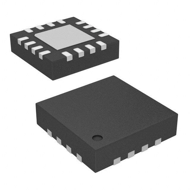
MCP453X/455X/463X/465X 2 7/8-Bit Single/Dual I C Digital POT with Volatile Memory Features Description • Single or Dual Resistor Network options The MCP45XX and MCP46XX devices offer a wide • Potentiometer or Rheostat configuration options range of product offerings using an I2C interface. This • Resistor Network Resolution family of devices support 7-bit and 8-bit resistor - 7-bit: 128 Resistors (129 Steps) networks, Volatile memory configurations, and Potenti- - 8-bit: 256 Resistors (257 Steps) ometer and Rheostat pinouts. • R Resistances options of: AB - 5kΩ Package Types (top view) - 10kΩ MCP45X1 MCP45X2 - 50kΩ Single Potentiometer Single Rheostat - 100kΩ • Zero-Scale to Full-Scale Wiper operation HVC / A0 1 8 VDD HVC / A0 1 8 VDD • Low Wiper Resistance: 75Ω (typical) SCL 2 7 P0B SCL 2 7 A1 • Low Tempco: SDA 3 6 P0W SDA 3 6 P0B V 4 5 P0A V 4 5 P0W - Absolute (Rheostat): 50ppm typical SS SS (0°C to 70°C) MSOP MSOP - Ratiometric (Potentiometer): 15ppm typical • I2C Serial interface HVC / A0 1 8 V HVC / A0 1 8 V DD DD - 100kHz, 400kHz and 3.4MHz support SCL 2 EP 7 A1 SCL 2 EP 7 A1 • Serial protocol allows: SDA 3 9 6 P0B SDA 3 9 6 P0B - High-Speed Read/Write to wiper V 4 5 P0W V 4 5 P0W SS SS - Increment/Decrement of wiper DFN 3x3 (MF) * DFN 3x3 (MF) * • Resistor Network Terminal Disconnect Feature via the Terminal Control (TCON) Register MCP46X1 Dual Potentiometers • Brown-out reset protection (1.5V typical) HVC/A0 1 14 VDD A0 • Serial Interface Inactive current (2.5uA typical) SCL 2 13 A1 C/ D • High-Voltage Tolerant Digital Inputs: Up to 12.5V SDA 3 12 A2 HV VDA1A2 • Wide Operating Voltage: VSS 4 11 NC 16151413 P1B 5 10 P0B SCL 1 12NC - 2.7V to 5.5V - Device Characteristics Specified P1W 6 9 P0W - 1.8V to 5.5V - Device Operation P1A 7 8 P0A SDA 2 EP 11NC V 3 17 10P0B • Wide Bandwidth (-3dB) Operation: SS - 2MHz (typical) for 5.0kΩ device TSSOP VSS 4 9 P0W 5 6 7 8 • Extended temperature range (-40°C to +125°C) BWA A P1P1P1 P0 QFN-16 4x4 (ML) * MCP46X2 Dual Rheostat HVC/A0 1 10 VDD HVC / A0 1 10VDD SCL 2 9 A1 SCL 2 9 A1 SDA 3 8 P0B SDA 3 EP 8 P0B PV1SBS 45 76 PP10WW VSS 4 11 7 P0W P1B 5 6 P1W MSOP DFN 3x3 (MF) * * Includes Exposed Thermal Pad (EP); see Table3-1. © 2008 Microchip Technology Inc. DS22096A-page 1
MCP453X/455X/463X/465X Device Block Diagram VDD Power-up/ Resistor P0A Brown-out V Network 0 SS Control (Pot 0) P0W A2 I2C Serial Wiper 0 & TCON A1 Interface Register Module & HVC/A0 P0B Control SCL Logic I2C Interface SDA (WiperLock™ Resistor P1A Technology) Network 1 (Pot 1) P1W Wiper 1 Memory (16x9) & TCON Wiper0 (V & NV) Register P1B Wiper1 (V & NV) TCON Reserved For Dual Resistor Network Devices Only Device Features Device # of POTs ConWfigipuerar tion Control Interface Memory Type WiperLock Technology POR Wiper Setting RARB eOspisttiaonncse ( k(tΩy)picaW-l( )iRΩpW)er # of Steps ORpaeVnrgDaDeti n(2g) MCP4531 (3) 1 Potentiometer (1) I2C RAM No Mid-Scale 5.0, 10.0, 50.0, 100.0 75 129 1.8V to 5.5V MCP4532 (3) 1 Rheostat I2C RAM No Mid-Scale 5.0, 10.0, 50.0, 100.0 75 129 1.8V to 5.5V MCP4541 1 Potentiometer (1) I2C EE Yes NV Wiper 5.0, 10.0, 50.0, 100.0 75 129 2.7V to 5.5V MCP4542 1 Rheostat I2C EE Yes NV Wiper 5.0, 10.0, 50.0, 100.0 75 129 2.7V to 5.5V MCP4551 (3) 1 Potentiometer (1) I2C RAM No Mid-Scale 5.0, 10.0, 50.0, 100.0 75 257 1.8V to 5.5V MCP4552 (3) 1 Rheostat I2C RAM No Mid-Scale 5.0, 10.0, 50.0, 100.0 75 257 1.8V to 5.5V MCP4561 1 Potentiometer (1) I2C EE Yes NV Wiper 5.0, 10.0, 50.0, 100.0 75 257 2.7V to 5.5V MCP4562 1 Rheostat I2C EE Yes NV Wiper 5.0, 10.0, 50.0, 100.0 75 257 2.7V to 5.5V MCP4631 (3) 2 Potentiometer (1) I2C RAM No Mid-Scale 5.0, 10.0, 50.0, 100.0 75 129 1.8V to 5.5V MCP4632 (3) 2 Rheostat I2C RAM No Mid-Scale 5.0, 10.0, 50.0, 100.0 75 129 1.8V to 5.5V MCP4641 2 Potentiometer (1) I2C EE Yes NV Wiper 5.0, 10.0, 50.0, 100.0 75 129 2.7V to 5.5V MCP4642 2 Rheostat I2C EE Yes NV Wiper 5.0, 10.0, 50.0, 100.0 75 129 2.7V to 5.5V MCP4651 (3) 2 Potentiometer (1) I2C RAM No Mid-Scale 5.0, 10.0, 50.0, 100.0 75 257 1.8V to 5.5V MCP4652 (3) 2 Rheostat I2C RAM No Mid-Scale 5.0, 10.0, 50.0, 100.0 75 257 1.8V to 5.5V MCP4661 2 Potentiometer (1) I2C EE Yes NV Wiper 5.0, 10.0, 50.0, 100.0 75 257 2.7V to 5.5V MCP4662 2 Rheostat I2C EE Yes NV Wiper 5.0, 10.0, 50.0, 100.0 75 257 2.7V to 5.5V Note 1: Floating either terminal (A or B) allows the device to be used as a Rheostat (variable resistor). 2: Analog characteristics only tested from 2.7V to 5.5V unless otherwise noted. 3: Please check Microchip web site for device release and availability DS22096A-page 2 © 2008 Microchip Technology Inc.
MCP453X/455X/463X/465X 1.0 ELECTRICAL † Notice: Stresses above those listed under “Maximum Ratings” may cause permanent damage to the device. This is CHARACTERISTICS a stress rating only and functional operation of the device at those or any other conditions above those indicated in the Absolute Maximum Ratings † operational listings of this specification is not implied. Exposure to maximum rating conditions for extended periods Voltage on VDD with respect to VSS............... -0.6V to +7.0V may affect device reliability. Voltage on HVC/A0, A1, A2, SCL, and SDA with respect to V -0.6V to 12.5V SS............................................................................. Voltage on all other pins (PxA, PxW, and PxB) with respect to V -0.3V to V + 0.3V SS......................................... DD Input clamp current, I IK (VI < 0, VI > VDD, VI > VPP ON HV pins)......................±20mA Output clamp current, I OK (V < 0 or V > V )..................................................±20mA O O DD Maximum output current sunk by any Output pin ......................................................................................25mA Maximum output current sourced by any Output pin ......................................................................................25mA Maximum current out of V pin.................................100mA SS Maximum current into V pin....................................100mA DD Maximum current into PXA, PXW & PXB pins............±2.5mA Storage temperature ....................................-65°C to +150°C Ambient temperature with power applied -40°C to +125°C Total power dissipation (Note 1)................................400mW Soldering temperature of leads (10 seconds).............+300°C ESD protection on all pins ..................................≥ 4kV (HBM), .......................................................................... ≥ 300V (MM) Maximum Junction Temperature (T ) .........................+150°C J Note 1: Power dissipation is calculated as follows: P = V x {I - ∑ I } + ∑ {(V -V ) x I } + ∑(V x I ) DIS DD DD OH DD OH OH OL OL © 2008 Microchip Technology Inc. DS22096A-page 3
MCP453X/455X/463X/465X AC/DC CHARACTERISTICS Standard Operating Conditions (unless otherwise specified) Operating Temperature –40°C ≤ T ≤ +125°C (extended) A DC Characteristics All parameters apply across the specified operating ranges unless noted. V = +2.7V to 5.5V, 5kΩ, 10kΩ, 50kΩ, 100kΩ devices. DD Typical specifications represent values for V = 5.5V, T = +25°C. DD A Parameters Sym Min Typ Max Units Conditions Supply Voltage V 2.7 — 5.5 V DD 1.8 — 2.7 V Serial Interface only. HVC pin Voltage V V — 12.5V V V ≥ The HVC pin will be at one HV SS DD Range 4.5V of three input levels (V , V or V ). (Note6) V — V + V V < IL IH IHH SS DD DD 8.0V 4.5V VDD Start Voltage VBOR — — 1.65 V RAM retention voltage (VRAM) < VBOR to ensure Wiper Reset VDD Rise Rate to VDDRR (Note9) V/ms ensure Power-on Reset Delay after device T — 10 20 µs BORD exits the reset state (V > V ) DD BOR Supply Current I — — 600 µA Serial Interface Active, DD (Note10) HVC/A0 = V (or V ) (Note11) IH IL Write all 0’s to Volatile Wiper 0 V = 5.5V, F = 3.4MHz DD SCL — — 250 µA Serial Interface Active, HVC/A0 = V (or V ) (Note11) IH IL Write all 0’s to Volatile Wiper 0 V = 5.5V, F = 100kHz DD SCL — 2.5 5 µA Serial Interface Inactive, (Stop condition, SCL = SDA = V ), IH Wiper = 0 V = 5.5V, HVC/A0 = V DD IH Note 1: Resistance is defined as the resistance between terminal A to terminal B. 2: INL and DNL are measured at V with V = V and V = V . W A DD B SS 3: MCP4XX1 only. 4: MCP4XX2 only, includes V and V . WZSE WFSE 5: Resistor terminals A, W and B’s polarity with respect to each other is not restricted. 6: This specification by design. 7: Non-linearity is affected by wiper resistance (R ), which changes significantly overvoltage and W temperature. 8: The MCP4XX1 is externally connected to match the configurations of the MCP45X2 and MCP46X2, and then tested. 9: POR/BOR is not rate dependent. 10: Supply current is independent of current through the resistor network 11: When HVC/A0 = V , the I current is less due to current into the HVC/A0 pin. See I specification IHH DD PU DS22096A-page 4 © 2008 Microchip Technology Inc.
MCP453X/455X/463X/465X AC/DC CHARACTERISTICS (CONTINUED) Standard Operating Conditions (unless otherwise specified) Operating Temperature –40°C ≤ T ≤ +125°C (extended) A DC Characteristics All parameters apply across the specified operating ranges unless noted. V = +2.7V to 5.5V, 5kΩ, 10kΩ, 50kΩ, 100kΩ devices. DD Typical specifications represent values for V = 5.5V, T = +25°C. DD A Parameters Sym Min Typ Max Units Conditions Resistance R 4.0 5 6.0 kΩ -502 devices (Note1) AB (± 20%) 8.0 10 12.0 kΩ -103 devices (Note1) 40.0 50 60.0 kΩ -503 devices (Note1) 80.0 100 120.0 kΩ -104 devices (Note1) Resolution N 257 Taps 8-bit No Missing Codes 129 Taps 7-bit No Missing Codes Step Resistance R — R / — Ω 8-bit Note6 S AB (256) — R / — Ω 7-bit Note6 AB (128) Nominal |R - R | / — 0.2 1.25 % MCP46X1 devices only AB0 AB1 Resistance Match R AB |R - R | — 0.25 1.5 % MCP46X2 devices only, BW0 BW1 / R Code = Full-Scale BW Wiper Resistance R — 75 160 Ω V = 5.5 V, I = 2.0mA, code = 00h W DD W (Note3, Note4) — 75 300 Ω V = 2.7 V, I = 2.0mA, code = 00h DD W Nominal ΔR /ΔT — 50 — ppm/°C T = -20°C to +70°C AB A Resistance — 100 — ppm/°C T = -40°C to +85°C A Tempco — 150 — ppm/°C T = -40°C to +125°C A Ratiometeric ΔV /ΔT — 15 — ppm/°C Code = Midscale (80h or 40h) WB Tempco Resistor Terminal V V V Vss — V V Note5, Note6 A, W, B DD Input Voltage Range (Terminals A, B and W) Note 1: Resistance is defined as the resistance between terminal A to terminal B. 2: INL and DNL are measured at V with V = V and V = V . W A DD B SS 3: MCP4XX1 only. 4: MCP4XX2 only, includes V and V . WZSE WFSE 5: Resistor terminals A, W and B’s polarity with respect to each other is not restricted. 6: This specification by design. 7: Non-linearity is affected by wiper resistance (R ), which changes significantly overvoltage and W temperature. 8: The MCP4XX1 is externally connected to match the configurations of the MCP45X2 and MCP46X2, and then tested. 9: POR/BOR is not rate dependent. 10: Supply current is independent of current through the resistor network 11: When HVC/A0 = V , the I current is less due to current into the HVC/A0 pin. See I specification IHH DD PU © 2008 Microchip Technology Inc. DS22096A-page 5
MCP453X/455X/463X/465X AC/DC CHARACTERISTICS (CONTINUED) Standard Operating Conditions (unless otherwise specified) Operating Temperature –40°C ≤ T ≤ +125°C (extended) A DC Characteristics All parameters apply across the specified operating ranges unless noted. V = +2.7V to 5.5V, 5kΩ, 10kΩ, 50kΩ, 100kΩ devices. DD Typical specifications represent values for V = 5.5V, T = +25°C. DD A Parameters Sym Min Typ Max Units Conditions Maximum current I — — 2.5 mA Terminal A I , T AW through Terminal W = Full-Scale (FS) (A, W or B) — — 2.5 mA Terminal B I , BW Note6 W = Zero Scale (ZS) — — 2.5 mA Terminal W I or I , AW BW W = FS or ZS — — 1.38 mA I , V = 0V, AB B V = 5.5V, A R = 4000 AB(MIN) — — 0.688 mA I , V = 0V, AB B V = 5.5V, Terminal A A R = 8000 and AB(MIN) — — 0.138 mA I , V = 0V, Terminal B AB B V = 5.5V, A R = 40000 AB(MIN) — — 0.069 mA I , V = 0V, AB B V = 5.5V, A R = 80000 AB(MIN) Leakage current I — 100 — nA MCP4XX1 PxA = PxW = PxB = V WL SS into A, W or B — 100 — nA MCP4XX2 PxB = PxW = V SS — 100 — nA Terminals Disconnected (R1HW = R0HW = 0) Note 1: Resistance is defined as the resistance between terminal A to terminal B. 2: INL and DNL are measured at V with V = V and V = V . W A DD B SS 3: MCP4XX1 only. 4: MCP4XX2 only, includes V and V . WZSE WFSE 5: Resistor terminals A, W and B’s polarity with respect to each other is not restricted. 6: This specification by design. 7: Non-linearity is affected by wiper resistance (R ), which changes significantly overvoltage and W temperature. 8: The MCP4XX1 is externally connected to match the configurations of the MCP45X2 and MCP46X2, and then tested. 9: POR/BOR is not rate dependent. 10: Supply current is independent of current through the resistor network 11: When HVC/A0 = V , the I current is less due to current into the HVC/A0 pin. See I specification IHH DD PU DS22096A-page 6 © 2008 Microchip Technology Inc.
MCP453X/455X/463X/465X AC/DC CHARACTERISTICS (CONTINUED) Standard Operating Conditions (unless otherwise specified) Operating Temperature –40°C ≤ T ≤ +125°C (extended) A DC Characteristics All parameters apply across the specified operating ranges unless noted. V = +2.7V to 5.5V, 5kΩ, 10kΩ, 50kΩ, 100kΩ devices. DD Typical specifications represent values for V = 5.5V, T = +25°C. DD A Parameters Sym Min Typ Max Units Conditions Full-Scale Error V -6.0 -0.1 — LSb 5kΩ 8-bit 3.0V ≤ V ≤ 5.5V WFSE DD (MCP4XX1 only) -4.0 -0.1 — LSb 7-bit 3.0V ≤ V ≤ 5.5V DD (8-bit code = 100h, -3.5 -0.1 — LSb 10kΩ 8-bit 3.0V ≤ V ≤ 5.5V 7-bit code = 80h) DD -2.0 -0.1 — LSb 7-bit 3.0V ≤ V ≤ 5.5V DD -0.8 -0.1 — LSb 50kΩ 8-bit 3.0V ≤ V ≤ 5.5V DD -0.5 -0.1 — LSb 7-bit 3.0V ≤ V ≤ 5.5V DD -0.5 -0.1 — LSb 100kΩ 8-bit 3.0V ≤ V ≤ 5.5V DD -0.5 -0.1 — LSb 7-bit 3.0V ≤ V ≤ 5.5V DD Zero-Scale Error V — +0.1 +6.0 LSb 5kΩ 8-bit 3.0V ≤ V ≤ 5.5V WZSE DD (MCP4XX1 only) — +0.1 +3.0 LSb 7-bit 3.0V ≤ V ≤ 5.5V DD (8-bit code = 00h, — +0.1 +3.5 LSb 10kΩ 8-bit 3.0V ≤ V ≤ 5.5V 7-bit code = 00h) DD — +0.1 +2.0 LSb 7-bit 3.0V ≤ V ≤ 5.5V DD — +0.1 +0.8 LSb 50kΩ 8-bit 3.0V ≤ V ≤ 5.5V DD — +0.1 +0.5 LSb 7-bit 3.0V ≤ V ≤ 5.5V DD — +0.1 +0.5 LSb 100kΩ 8-bit 3.0V ≤ V ≤ 5.5V DD — +0.1 +0.5 LSb 7-bit 3.0V ≤ V ≤ 5.5V DD Potentiometer INL -1 ±0.5 +1 LSb 8-bit 3.0V ≤ V ≤ 5.5V DD Integral MCP4XX1 devices only -0.5 ±0.25 +0.5 LSb 7-bit Non-linearity (Note2) Potentiometer DNL -0.5 ±0.25 +0.5 LSb 8-bit 3.0V ≤ V ≤ 5.5V DD Differential MCP4XX1 devices only -0.25 ±0.125 +0.25 LSb 7-bit Non-linearity (Note2) Note 1: Resistance is defined as the resistance between terminal A to terminal B. 2: INL and DNL are measured at V with V = V and V = V . W A DD B SS 3: MCP4XX1 only. 4: MCP4XX2 only, includes V and V . WZSE WFSE 5: Resistor terminals A, W and B’s polarity with respect to each other is not restricted. 6: This specification by design. 7: Non-linearity is affected by wiper resistance (R ), which changes significantly overvoltage and W temperature. 8: The MCP4XX1 is externally connected to match the configurations of the MCP45X2 and MCP46X2, and then tested. 9: POR/BOR is not rate dependent. 10: Supply current is independent of current through the resistor network 11: When HVC/A0 = V , the I current is less due to current into the HVC/A0 pin. See I specification IHH DD PU © 2008 Microchip Technology Inc. DS22096A-page 7
MCP453X/455X/463X/465X AC/DC CHARACTERISTICS (CONTINUED) Standard Operating Conditions (unless otherwise specified) Operating Temperature –40°C ≤ T ≤ +125°C (extended) A DC Characteristics All parameters apply across the specified operating ranges unless noted. V = +2.7V to 5.5V, 5kΩ, 10kΩ, 50kΩ, 100kΩ devices. DD Typical specifications represent values for V = 5.5V, T = +25°C. DD A Parameters Sym Min Typ Max Units Conditions Bandwidth -3dB BW — 2 — MHz 5kΩ 8-bit Code = 80h (See Figure2-65, — 2 — MHz 7-bit Code = 40h load = 30pF) — 1 — MHz 10kΩ 8-bit Code = 80h — 1 — MHz 7-bit Code = 40h — 200 — kHz 50kΩ 8-bit Code = 80h — 200 — kHz 7-bit Code = 40h — 100 — kHz 100kΩ 8-bit Code = 80h — 100 — kHz 7-bit Code = 40h Note 1: Resistance is defined as the resistance between terminal A to terminal B. 2: INL and DNL are measured at V with V = V and V = V . W A DD B SS 3: MCP4XX1 only. 4: MCP4XX2 only, includes V and V . WZSE WFSE 5: Resistor terminals A, W and B’s polarity with respect to each other is not restricted. 6: This specification by design. 7: Non-linearity is affected by wiper resistance (R ), which changes significantly overvoltage and W temperature. 8: The MCP4XX1 is externally connected to match the configurations of the MCP45X2 and MCP46X2, and then tested. 9: POR/BOR is not rate dependent. 10: Supply current is independent of current through the resistor network 11: When HVC/A0 = V , the I current is less due to current into the HVC/A0 pin. See I specification IHH DD PU DS22096A-page 8 © 2008 Microchip Technology Inc.
MCP453X/455X/463X/465X AC/DC CHARACTERISTICS (CONTINUED) Standard Operating Conditions (unless otherwise specified) Operating Temperature –40°C ≤ T ≤ +125°C (extended) A DC Characteristics All parameters apply across the specified operating ranges unless noted. V = +2.7V to 5.5V, 5kΩ, 10kΩ, 50kΩ, 100kΩ devices. DD Typical specifications represent values for V = 5.5V, T = +25°C. DD A Parameters Sym Min Typ Max Units Conditions Rheostat Integral R-INL -1.5 ±0.5 +1.5 LSb 5kΩ 8-bit 5.5V, I = 900µA W Non-linearity -8.25 +4.5 +8.25 LSb 3.0V, I = 480µA W MCP45X1 (Note7) (Note4, Note8) -1.125 ±0.5 +1.125 LSb 7-bit 5.5V, I = 900µA MCP4XX2 devices W only (Note4) -6.0 +4.5 +6.0 LSb 3.0V, IW = 480µA (Note7) -1.5 ±0.5 +1.5 LSb 10kΩ 8-bit 5.5V, I = 450µA W -5.5 +2.5 +5.5 LSb 3.0V, I = 240µA W (Note7) -1.125 ±0.5 +1.125 LSb 7-bit 5.5V, I = 450µA W -4.0 +2.5 +4.0 LSb 3.0V, I = 240µA W (Note7) -1.5 ±0.5 +1.5 LSb 50kΩ 8-bit 5.5V, I = 90µA W -2.0 +1 +2.0 LSb 3.0V, I = 48µA W (Note7) -1.125 ±0.5 +1.125 LSb 7-bit 5.5V, I = 90µA W -1.5 +1 +1.5 LSb 3.0V, I = 48µA W (Note7) -1.0 ±0.5 +1.0 LSb 100kΩ 8-bit 5.5V, I = 45µA W -1.5 +0.25 +1.5 LSb 3.0V, I = 24µA W (Note7) -0.8 ±0.5 +0.8 LSb 7-bit 5.5V, I = 45µA W -1.125 +0.25 +1.125 LSb 3.0V, I = 24µA W (Note7) Note 1: Resistance is defined as the resistance between terminal A to terminal B. 2: INL and DNL are measured at V with V = V and V = V . W A DD B SS 3: MCP4XX1 only. 4: MCP4XX2 only, includes V and V . WZSE WFSE 5: Resistor terminals A, W and B’s polarity with respect to each other is not restricted. 6: This specification by design. 7: Non-linearity is affected by wiper resistance (R ), which changes significantly overvoltage and W temperature. 8: The MCP4XX1 is externally connected to match the configurations of the MCP45X2 and MCP46X2, and then tested. 9: POR/BOR is not rate dependent. 10: Supply current is independent of current through the resistor network 11: When HVC/A0 = V , the I current is less due to current into the HVC/A0 pin. See I specification IHH DD PU © 2008 Microchip Technology Inc. DS22096A-page 9
MCP453X/455X/463X/465X AC/DC CHARACTERISTICS (CONTINUED) Standard Operating Conditions (unless otherwise specified) Operating Temperature –40°C ≤ T ≤ +125°C (extended) A DC Characteristics All parameters apply across the specified operating ranges unless noted. V = +2.7V to 5.5V, 5kΩ, 10kΩ, 50kΩ, 100kΩ devices. DD Typical specifications represent values for V = 5.5V, T = +25°C. DD A Parameters Sym Min Typ Max Units Conditions Rheostat R-DNL -0.5 ±0.25 +0.5 LSb 5kΩ 8-bit 5.5V, I = 900µA W Differential -1.0 +0.5 +1.0 LSb 3.0V, I = 480µA W Non-linearity (Note7) MCP45X1 -0.375 ±0.25 +0.375 LSb 7-bit 5.5V, I = 900µA (Note4, Note8) W MCP4XX2 devices -0.75 +0.5 +0.75 LSb 3.0V, IW = 480µA only (Note7) (Note4) -0.5 ±0.25 +0.5 LSb 10kΩ 8-bit 5.5V, I = 450µA W -1.0 +0.25 +1.0 LSb 3.0V, I = 240µA W (Note7) -0.375 ±0.25 +0.375 LSb 7-bit 5.5V, I = 450µA W -0.75 +0.5 +0.75 LSb 3.0V, I = 240µA W (Note7) -0.5 ±0.25 +0.5 LSb 50kΩ 8-bit 5.5V, I = 90µA W -0.5 ±0.25 +0.5 LSb 3.0V, I = 48µA W (Note7) -0.375 ±0.25 +0.375 LSb 7-bit 5.5V, I = 90µA W -0.375 ±0.25 +0.375 LSb 3.0V, I = 48µA W (Note7) -0.5 ±0.25 +0.5 LSb 100kΩ 8-bit 5.5V, I = 45µA W -0.5 ±0.25 +0.5 LSb 3.0V, I = 24µA W (Note7) -0.375 ±0.25 +0.375 LSb 7-bit 5.5V, I = 45µA W -0.375 ±0.25 +0.375 LSb 3.0V, I = 24µA W (Note7) Capacitance (P ) C — 75 — pF f =1MHz, Code = Full-Scale A AW Capacitance (P ) C — 120 — pF f =1MHz, Code = Full-Scale w W Capacitance (P ) C — 75 — pF f =1MHz, Code = Full-Scale B BW Note 1: Resistance is defined as the resistance between terminal A to terminal B. 2: INL and DNL are measured at V with V = V and V = V . W A DD B SS 3: MCP4XX1 only. 4: MCP4XX2 only, includes V and V . WZSE WFSE 5: Resistor terminals A, W and B’s polarity with respect to each other is not restricted. 6: This specification by design. 7: Non-linearity is affected by wiper resistance (R ), which changes significantly overvoltage and W temperature. 8: The MCP4XX1 is externally connected to match the configurations of the MCP45X2 and MCP46X2, and then tested. 9: POR/BOR is not rate dependent. 10: Supply current is independent of current through the resistor network 11: When HVC/A0 = V , the I current is less due to current into the HVC/A0 pin. See I specification IHH DD PU DS22096A-page 10 © 2008 Microchip Technology Inc.
MCP453X/455X/463X/465X AC/DC CHARACTERISTICS (CONTINUED) Standard Operating Conditions (unless otherwise specified) Operating Temperature –40°C ≤ T ≤ +125°C (extended) A DC Characteristics All parameters apply across the specified operating ranges unless noted. V = +2.7V to 5.5V, 5kΩ, 10kΩ, 50kΩ, 100kΩ devices. DD Typical specifications represent values for V = 5.5V, T = +25°C. DD A Parameters Sym Min Typ Max Units Conditions Digital Inputs/Outputs (SDA, SCK, HVC/A0, A1, A2, WP) Schmitt Trigger V 0.45V — — V All 2.7V ≤ V ≤ 5.5V IH DD DD High Input Inputs (Allows 2.7V Digital V with DD Threshold except 5V Analog V ) DD SDA 0.5V — — V 1.8V ≤ V ≤ 2.7V DD DD and SCL 0.7V — V V 100kHz DD MAX SDA 0.7V — V V 400kHz DD MAX and 0.7V — V V 1.7MHz DD MAX SCL 0.7V — V V 3.4Mhz DD MAX Schmitt Trigger V — — 0.2V V All inputs except SDA and SCL IL DD Low Input -0.5 — 0.3V V 100kHz DD Threshold SDA -0.5 — 0.3V V 400kHz DD and -0.5 — 0.3V V 1.7MHz DD SCL -0.5 — 0.3V V 3.4Mhz DD Hysteresis of V — 0.1V — V All inputs except SDA and SCL HYS DD Schmitt Trigger N.A. — — V V < 2.0V DD Inputs (Note6) 100kHz N.A. — — V V ≥ 2.0V DD SDA 0.1V — — V V < 2.0V DD DD and 400kHz 0.05V — — V V ≥ 2.0V DD SCL DD 0.1V — — V 1.7MHz DD 0.1V — — V 3.4Mhz DD High Voltage Limit V — — 12.5 (6) V Pin can tolerate V or less. MAX MAX Note 1: Resistance is defined as the resistance between terminal A to terminal B. 2: INL and DNL are measured at V with V = V and V = V . W A DD B SS 3: MCP4XX1 only. 4: MCP4XX2 only, includes V and V . WZSE WFSE 5: Resistor terminals A, W and B’s polarity with respect to each other is not restricted. 6: This specification by design. 7: Non-linearity is affected by wiper resistance (R ), which changes significantly overvoltage and W temperature. 8: The MCP4XX1 is externally connected to match the configurations of the MCP45X2 and MCP46X2, and then tested. 9: POR/BOR is not rate dependent. 10: Supply current is independent of current through the resistor network 11: When HVC/A0 = V , the I current is less due to current into the HVC/A0 pin. See I specification IHH DD PU © 2008 Microchip Technology Inc. DS22096A-page 11
MCP453X/455X/463X/465X AC/DC CHARACTERISTICS (CONTINUED) Standard Operating Conditions (unless otherwise specified) Operating Temperature –40°C ≤ T ≤ +125°C (extended) A DC Characteristics All parameters apply across the specified operating ranges unless noted. V = +2.7V to 5.5V, 5kΩ, 10kΩ, 50kΩ, 100kΩ devices. DD Typical specifications represent values for V = 5.5V, T = +25°C. DD A Parameters Sym Min Typ Max Units Conditions Output Low V V — 0.2V V V < 2.0V, I = 1mA OL SS DD DD OL Voltage (SDA) V — 0.4 V V ≥ 2.0V, I = 3mA SS DD OL Weak Pull-up / I — — 1.75 mA Internal V pull-up, V pull-down PU DD IHH Pull-down Current V = 5.5V, V = 12.5V DD IHH — 170 — µA HVC pin, V = 5.5V, V = 3V DD HVC HVC Pull-up / R — 16 — kΩ V = 5.5V, V = 3V HVC DD HVC Pull-down Resistance Input Leakage Cur- I -1 — 1 µA V = V and V = V IL IN DD IN SS rent Pin Capacitance C , C — 10 — pF f = 3.4MHz IN OUT C RAM (Wiper) Value Value Range N 0h — 1FFh hex 8-bit device 0h — 1FFh hex 7-bit device TCON POR/BOR N 1FFh hex All Terminals connected TCON Value Power Requirements Power Supply PSS — 0.0015 0.0035 %/% 8-bit V = 2.7V to 5.5V, DD Sensitivity V = 2.7V, Code = 80h A (MCP45X2 and — 0.0015 0.0035 %/% 7-bit V = 2.7V to 5.5V, DD MCP46X2 only) V = 2.7V, Code = 40h A Note 1: Resistance is defined as the resistance between terminal A to terminal B. 2: INL and DNL are measured at V with V = V and V = V . W A DD B SS 3: MCP4XX1 only. 4: MCP4XX2 only, includes V and V . WZSE WFSE 5: Resistor terminals A, W and B’s polarity with respect to each other is not restricted. 6: This specification by design. 7: Non-linearity is affected by wiper resistance (R ), which changes significantly overvoltage and W temperature. 8: The MCP4XX1 is externally connected to match the configurations of the MCP45X2 and MCP46X2, and then tested. 9: POR/BOR is not rate dependent. 10: Supply current is independent of current through the resistor network 11: When HVC/A0 = V , the I current is less due to current into the HVC/A0 pin. See I specification IHH DD PU DS22096A-page 12 © 2008 Microchip Technology Inc.
MCP453X/455X/463X/465X SCL 91 93 90 92 SDA START STOP Condition Condition FIGURE 1-1: I2C Bus Start/Stop Bits Timing Waveforms. TABLE 1-1: I2C BUS START/STOP BITS REQUIREMENTS I2C AC Characteristics Standard Operating Conditions (unless otherwise specified) Operating Temperature –40°C ≤ TA ≤ +125°C (Extended) Operating Voltage VDD range is described in AC/DC characteristics Param. Symbol Characteristic Min Max Units Conditions No. F Standard Mode 0 100 kHz C = 400pF, 1.8V - 5.5V SCL b Fast Mode 0 400 kHz C = 400pF, 2.7V - 5.5V b High-Speed 1.7 0 1.7 MHz C = 400pF, 4.5V - 5.5V b High-Speed 3.4 0 3.4 MHz C = 100pF, 4.5V - 5.5V b D102 Cb Bus capacitive 100kHz mode — 400 pF loading 400kHz mode — 400 pF 1.7MHz mode — 400 pF 3.4MHz mode — 100 pF 90 TSU:STA START condition 100kHz mode 4700 — ns Only relevant for repeated Setup time 400kHz mode 600 — ns START condition 1.7MHz mode 160 — ns 3.4MHz mode 160 — ns 91 THD:STA START condition 100kHz mode 4000 — ns After this period the first Hold time 400kHz mode 600 — ns clock pulse is generated 1.7MHz mode 160 — ns 3.4MHz mode 160 — ns 92 TSU:STO STOP condition 100kHz mode 4000 — ns Setup time 400kHz mode 600 — ns 1.7MHz mode 160 — ns 3.4MHz mode 160 — ns 93 THD:STO STOP condition 100kHz mode 4000 — ns Hold time 400kHz mode 600 — ns 1.7MHz mode 160 — ns 3.4MHz mode 160 — ns © 2008 Microchip Technology Inc. DS22096A-page 13
MCP453X/455X/463X/465X 103 100 102 101 SCL 90 106 91 107 92 SDA In 109 109 110 SDA Out FIGURE 1-2: I2C Bus Data Timing. T ABLE 1-2: I2C BUS DATA REQUIREMENTS (SLAVE MODE) I2C AC Characteristics Standard Operating Conditions (unless otherwise specified) Operating Temperature –40°C ≤ TA ≤ +125°C (Extended) Operating Voltage V range is described in AC/DC characteristics DD Param. Sym Characteristic Min Max Units Conditions No. 100 THIGH Clock high time 100kHz mode 4000 — ns 1.8V-5.5V 400kHz mode 600 — ns 2.7V-5.5V 1.7MHz mode 120 ns 4.5V-5.5V 3.4MHz mode 60 — ns 4.5V-5.5V 101 TLOW Clock low time 100kHz mode 4700 — ns 1.8V-5.5V 400kHz mode 1300 — ns 2.7V-5.5V 1.7MHz mode 320 ns 4.5V-5.5V 3.4MHz mode 160 — ns 4.5V-5.5V Note 1: As a transmitter, the device must provide this internal minimum delay time to bridge the undefined region (minimum 300ns) of the falling edge of SCL to avoid unintended generation of START or STOP conditions. 2: A fast-mode (400kHz) I2C-bus device can be used in a standard-mode (100kHz) I2C-bus system, but the requirement t ≥250ns must then be met. This will automatically be the case if the device does not SU;DAT stretch the LOW period of the SCL signal. If such a device does stretch the LOW period of the SCL signal, it must output the next data bit to the SDA line T max.+t =1000+250=1250ns (according to the standard-mode I2C bus specification) before R SU;DAT the SCL line is released. 3: The MCP46X1/MCP46X2 device must provide a data hold time to bridge the undefined part between V IH and V of the falling edge of the SCL signal. This specification is not a part of the I2C specification, but IL must be tested in order to ensure that the output data will meet the setup and hold specifications for the receiving device. 4: Use Cb in pF for the calculations. 5: Not Tested 6: A Master Transmitter must provide a delay to ensure that difference between SDA and SCL fall times do not unintentionally create a Start or Stop condition. 7: Ensured by the T 3.4MHz specification test. AA DS22096A-page 14 © 2008 Microchip Technology Inc.
MCP453X/455X/463X/465X TABLE 1-2: I2C BUS DATA REQUIREMENTS (SLAVE MODE) (CONTINUED) I2C AC Characteristics Standard Operating Conditions (unless otherwise specified) Operating Temperature –40°C ≤ TA ≤ +125°C (Extended) Operating Voltage V range is described in AC/DC characteristics DD Param. Sym Characteristic Min Max Units Conditions No. 102A (5) TRSCL SCL rise time 100kHz mode — 1000 ns Cb is specified to be from 10 to 400pF (100pF maxi- 400kHz mode 20 + 0.1Cb 300 ns mum for 3.4MHz mode) 1.7MHz mode 20 80 ns 1.7MHz mode 20 160 ns After a Repeated Start con- dition or an Acknowledge bit 3.4MHz mode 10 40 ns 3.4MHz mode 10 80 ns After a Repeated Start condition or an Acknowl- edge bit 102B (5) TRSDA SDA rise time 100kHz mode — 1000 ns Cb is specified to be from 10 to 400pF (100pF max 400kHz mode 20 + 0.1Cb 300 ns for 3.4MHz mode) 1.7MHz mode 20 160 ns 3.4MHz mode 10 80 ns 103A (5) TFSCL SCL fall time 100kHz mode — 300 ns Cb is specified to be from 10 to 400pF (100pF max 400kHz mode 20 + 0.1Cb 300 ns for 3.4MHz mode) 1.7MHz mode 20 80 ns 3.4MHz mode 10 40 ns 103B (5) TFSDA SDA fall time 100kHz mode — 300 ns Cb is specified to be from 400kHz mode 20 + 0.1Cb (4) 300 ns 10 to 400pF (100pF max for 3.4MHz mode) 1.7MHz mode 20 160 ns 3.4MHz mode 10 80 ns 106 T Data input hold 100kHz mode 0 — ns 1.8V-5.5V, Note6 HD:DAT time 400kHz mode 0 — ns 2.7V-5.5V, Note6 1.7MHz mode 0 — ns 4.5V-5.5V, Note6 3.4MHz mode 0 — ns 4.5V-5.5V, Note6 Note 1: As a transmitter, the device must provide this internal minimum delay time to bridge the undefined region (minimum 300ns) of the falling edge of SCL to avoid unintended generation of START or STOP conditions. 2: A fast-mode (400kHz) I2C-bus device can be used in a standard-mode (100kHz) I2C-bus system, but the requirement t ≥250ns must then be met. This will automatically be the case if the device does not SU;DAT stretch the LOW period of the SCL signal. If such a device does stretch the LOW period of the SCL signal, it must output the next data bit to the SDA line T max.+t =1000+250=1250ns (according to the standard-mode I2C bus specification) before R SU;DAT the SCL line is released. 3: The MCP46X1/MCP46X2 device must provide a data hold time to bridge the undefined part between V IH and V of the falling edge of the SCL signal. This specification is not a part of the I2C specification, but IL must be tested in order to ensure that the output data will meet the setup and hold specifications for the receiving device. 4: Use Cb in pF for the calculations. 5: Not Tested 6: A Master Transmitter must provide a delay to ensure that difference between SDA and SCL fall times do not unintentionally create a Start or Stop condition. 7: Ensured by the T 3.4MHz specification test. AA © 2008 Microchip Technology Inc. DS22096A-page 15
MCP453X/455X/463X/465X TABLE 1-2: I2C BUS DATA REQUIREMENTS (SLAVE MODE) (CONTINUED) I2C AC Characteristics Standard Operating Conditions (unless otherwise specified) Operating Temperature –40°C ≤ TA ≤ +125°C (Extended) Operating Voltage V range is described in AC/DC characteristics DD Param. Sym Characteristic Min Max Units Conditions No. 107 T Data input setup 100kHz mode 250 — ns Note2 SU:DAT time 400kHz mode 100 — ns 1.7MHz mode 10 — ns 3.4MHz mode 10 — ns 109 T Output valid 100kHz mode — 3450 ns Note1 AA from clock 400kHz mode — 900 ns 1.7MHz mode — 150 ns Cb = 100pF, Note1, Note7 — 310 ns Cb = 400pF, Note1, Note5 3.4MHz mode — 150 ns Cb = 100pF, Note1 110 TBUF Bus free time 100kHz mode 4700 — ns Time the bus must be free before a new transmission 400kHz mode 1300 — ns can start 1.7MHz mode N.A. — ns 3.4MHz mode N.A. — ns T Input filter spike 100kHz mode — 50 ns Philips Spec states N.A. SP suppression 400kHz mode — 50 ns (SDA and SCL) 1.7MHz mode — 10 ns Spike suppression 3.4MHz mode — 10 ns Spike suppression Note 1: As a transmitter, the device must provide this internal minimum delay time to bridge the undefined region (minimum 300ns) of the falling edge of SCL to avoid unintended generation of START or STOP conditions. 2: A fast-mode (400kHz) I2C-bus device can be used in a standard-mode (100kHz) I2C-bus system, but the requirement t ≥250ns must then be met. This will automatically be the case if the device does not SU;DAT stretch the LOW period of the SCL signal. If such a device does stretch the LOW period of the SCL signal, it must output the next data bit to the SDA line T max.+t =1000+250=1250ns (according to the standard-mode I2C bus specification) before R SU;DAT the SCL line is released. 3: The MCP46X1/MCP46X2 device must provide a data hold time to bridge the undefined part between V IH and V of the falling edge of the SCL signal. This specification is not a part of the I2C specification, but IL must be tested in order to ensure that the output data will meet the setup and hold specifications for the receiving device. 4: Use Cb in pF for the calculations. 5: Not Tested 6: A Master Transmitter must provide a delay to ensure that difference between SDA and SCL fall times do not unintentionally create a Start or Stop condition. 7: Ensured by the T 3.4MHz specification test. AA DS22096A-page 16 © 2008 Microchip Technology Inc.
MCP453X/455X/463X/465X TEMPERATURE CHARACTERISTICS Electrical Specifications: Unless otherwise indicated, V =+2.7V to +5.5V, V =GND. DD SS Parameters Sym Min Typ Max Units Conditions Temperature Ranges Specified Temperature Range T -40 — +125 °C A Operating Temperature Range T -40 — +125 °C A Storage Temperature Range T -65 — +150 °C A Thermal Package Resistances Thermal Resistance, 8L-DFN (3x3) θ — 60 — °C/W JA Thermal Resistance, 8L-MSOP θ — 211 — °C/W JA Thermal Resistance, 8L-SOIC θ — 145.5 — °C/W JA Thermal Resistance, 10L-DFN (3x3) θ — 57 — °C/W JA Thermal Resistance, 10L-MSOP θ — 202 — °C/W JA Thermal Resistance, 14L-MSOP θ — N/A — °C/W JA Thermal Resistance, 14L-SOIC θ — 95.3 — °C/W JA Thermal Resistance, 16L-QFN θ — 47 — °C/W JA © 2008 Microchip Technology Inc. DS22096A-page 17
MCP453X/455X/463X/465X NOTES: DS22096A-page 18 © 2008 Microchip Technology Inc.
MCP453X/455X/463X/465X 2.0 TYPICAL PERFORMANCE CURVES Note: The graphs and tables provided following this note are a statistical summary based on a limited number of samples and are provided for informational purposes only. The performance characteristics listed herein are not tested or guaranteed. In some graphs or tables, the data presented may be outside the specified operating range (e.g., outside specified power supply range) and therefore outside the warranted range. Note: Unless otherwise indicated, T = +25°C, V = 5V, V = 0V. A DD SS 250 1000 450 3.4MHz, 5.5V 800 400 200 600 350 3.4MHz, 2.7V I (uA)DD 122350500000 1.7MHz, 2.7V 4001k10H.07zkM,H 5Hz.z5, ,V5 5.5.5VV R (kOhms)HVC110500 IHVC --0244200000000 I (µA)HVC 100 400kHz, 2.7V 100kHz, 2.7V 50 -600 50 RHVC -800 0 0 -1000 -40 0 40 80 120 2 3 4 5 6 7 8 9 10 Temperature (°C) V (V) HVC FIGURE 2-1: Device Current (I ) vs. I2C FIGURE 2-4: HVC Pull-up/Pull-down DD Frequency (f ) and Ambient Temperature Resistance (R ) and Current (I ) vs. HVC SCL HVC HVC (V = 2.7V and 5.5V). Input Voltage (V ) (V = 5.5V). DD HVC DD 3 12 dby (uA)2.25 5.5V hreshold (V) 1068 5.55.V5V E Exinttry 2.7V Entry n1.5 T Ista 1 C V PP 4 2.7V Exit V 2 2.7V H 0.5 0 -40 0 40 80 120 -40 -20 0 20 40 60 80 100 120 Temperature (°C) Ambient Temperature (°C) FIGURE 2-2: Device Current (I ) and FIGURE 2-5: HVC High Input Entry/Exit SHDN V . (HVC = V ) vs. Ambient Temperature. Threshold vs. Ambient Temperature and V . DD DD DD 420 400 A) 380 µ (RITE 360 5.5V IW 340 320 300 -40 0 40 80 120 Temperature (°C) FIGURE 2-3: Write Current (I ) vs. WRITE Ambient Temperature. © 2008 Microchip Technology Inc. DS22096A-page 19
MCP453X/455X/463X/465X Note: Unless otherwise indicated, T = +25°C, V = 5V, V = 0V. A DD SS 120 0.3 120 1.25 -40C Rw 25C Rw 85C Rw 125C Rw -40C Rw 25C Rw 85C Rw 125C Rw R) W 100 --4400CC IDNNLL 2255CC IDNNLL 8855CC IDNNLL 112255CC IDNNLL 0.2 R) W 100 --4400CC DINNLL 2255CC IDNNLL 8855CC IDNNLL 112255CC IDNNLL 0.75 Wiper Resistance ((ohms) 468000 125°C8D5N°CL -40°C 25°CINL RW --0000.1..21Error (LSb) Wiper Resistance ((ohms) 468000 125°C85°C 25°C-40°CINL RW DNL --000.2..72555Error (LSb) 20 -0.3 20 -1.25 0 32 64 96 128 160 192 224 256 0 32 64 96 128 160 192 224 256 Wiper Setting (decimal) Wiper Setting (decimal) FIGURE 2-6: 5kΩ Pot Mode – R (Ω), FIGURE 2-9: 5kΩ Rheo Mode – R (Ω), W W INL (LSb), DNL (LSb) vs. Wiper Setting and INL (LSb), DNL (LSb) vs. Wiper Setting and Ambient Temperature (V = 5.5V). Ambient Temperature (V = 5.5V). DD DD 300 300 0.3 -40C Rw 25C Rw 85C Rw 125C Rw ) W 260 ---444000CCC DRINNwLL 222555CCC IRDNwNLL 888555CCC IRDNwNLL 111222555CCC IRDNwNLL 0.2 ) W 260 --4400CC IDNNLL 2255CC IDNNLL 8855CC IDNNLL 112255CC IDNNLL 6 Wiper Resistance (R(ohms)11120482600000 DNL 85°C12I5N°RLCW --0000.1..21Error (LSb) Wiper Resistance (R(ohms)11120482600000 -40°C RW INL 024 Error (LSb) -40°C 25°C 125°C 85°C25°C DNL 20 -0.3 20 -2 0 32 64 96 128 160 192 224 256 0 32 64 96 128 160 192 224 256 Wiper Setting (decimal) Wiper Setting (decimal) FIGURE 2-7: 5kΩ Pot Mode – R (Ω), FIGURE 2-10: 5kΩ Rheo Mode – R (Ω), W W INL (LSb), DNL (LSb) vs. Wiper Setting and INL (LSb), DNL (LSb) vs. Wiper Setting and Ambient Temperature (V = 3.0V). Ambient Temperature (V = 3.0V). DD DD 0.5 -40C Rw 25C Rw 85C Rw 125C Rw 118 Wiper Resistance (R) W(ohms)1122050550000000000 IN---444L000CCC DRINNwLL 222555CCC RDINwNLL 888555CCC RIDNDwNLLNL 111222555CCC RIDNwNLL --0000000....1234..21Error (LSb) Wiper Resistance (R) W(ohms)1122050550000000000 --4400CC DINRNLWL 2255CC DINNLL 8855CC DINDNILNNLLL 112255CC IDNNLL 1357988888 Error (LSb) RW 0 -0.3 0 -2 0 64 128 192 256 0 64 128 192 256 Wiper Setting (decimal) Wiper Setting (decimal) Note: Refer to AN1080 for additional informa- Note: Refer to AN1080 for additional informa- tion on the characteristics of the wiper tion on the characteristics of the wiper resistance (R ) with respect to device resistance (R ) with respect to device W W voltage and wiper setting value. voltage and wiper setting value. FIGURE 2-8: 5kΩ Pot Mode – R (Ω), FIGURE 2-11: 5kΩ Rheo Mode – R (Ω), W W INL (LSb), DNL (LSb) vs. Wiper Setting and INL (LSb), DNL (LSb) vs. Wiper Setting and Ambient Temperature (V = 1.8V). Ambient Temperature (V = 1.8V). DD DD DS22096A-page 20 © 2008 Microchip Technology Inc.
MCP453X/455X/463X/465X Note: Unless otherwise indicated, T = +25°C, V = 5V, V = 0V. A DD SS 5300 6000 ) B RA 5250 5000 e ( al Resistanc(Ohms) 55125000 2.7V R (Ohms)WB234000000000 -40°C n mi 5100 1000 25°C o 5.5V 85°C N 125°C 5050 0 -40 0 40 80 120 0 32 64 96 128 160 192 224 256 Ambient Temperature (°C) Wiper Setting (decimal) FIGURE 2-12: 5kΩ – Nominal Resistance FIGURE 2-13: 5kΩ – R (Ω) vs. Wiper WB (Ω) vs. Ambient Temperature and V . Setting and Ambient Temperature. DD © 2008 Microchip Technology Inc. DS22096A-page 21
MCP453X/455X/463X/465X Note: Unless otherwise indicated, T = +25°C, V = 5V, V = 0V. A DD SS FIGURE 2-14: 5kΩ – Low-Voltage FIGURE 2-17: 5kΩ – Low-Voltage Decrement Wiper Settling Time (V = 5.5V) Increment Wiper Settling Time (V = 5.5V) DD DD (1µs/Div). (1µs/Div). FIGURE 2-15: 5kΩ – Low-Voltage FIGURE 2-18: 5kΩ – Low-Voltage Decrement Wiper Settling Time (V = 2.7V) Increment Wiper Settling Time (V = 2.7V) DD DD (1µs/Div). (1µs/Div). FIGURE 2-16: 5kΩ – Power-Up Wiper Response Time (20ms/Div). DS22096A-page 22 © 2008 Microchip Technology Inc.
MCP453X/455X/463X/465X Note: Unless otherwise indicated, T = +25°C, V = 5V, V = 0V. A DD SS 120 0.3 120 1 -40C Rw 25C Rw 85C Rw 125C Rw -40C Rw 25C Rw 85C Rw 125C Rw ) W 100 --4400CC IDNNLL 2255CC IDNNLL 8855CC IDNNLL 112255CC IDNNLL 0.2 ) W 100 --4400CC IDNNLL 2255CC IDNNLL 8855CC IDNNLL 112255CC IDNNLL R R 0.5 Wiper Resistance ((ohms) 468000 125°C 85D°CN2L5°C -40°C INL RW --0000.1..21Error (LSb) Wiper Resistance ((ohms) 468000 125°C85°C 25°C -40°INCL RW DNL -00.5Error (LSb) 20 -0.3 20 -1 0 25 50 75 100125150175200225250 0 32 64 96 128 160 192 224 256 Wiper Setting (decimal) Wiper Setting (decimal) FIGURE 2-19: 10kΩ Pot Mode – R (Ω), FIGURE 2-22: 10kΩ Rheo Mode – R (Ω), W W INL (LSb), DNL (LSb) vs. Wiper Setting and INL (LSb), DNL (LSb) vs. Wiper Setting and Ambient Temperature (V = 5.5V). Ambient Temperature (V = 5.5V). DD DD 300 4 300 0.3 -40C Rw 25C Rw 85C Rw 125C Rw -40C Rw 25C Rw 85C Rw 125C Rw -40C INL 25C INL 85C INL 125C INL ) W 260 --4400CC DINNLL 2255CC IDNNLL 8855CC IDNNLL 112255CC IDNNLL 0.2 ) W 260 -40C DNL 25C DNL 85C DNL 125C DNL 3 R R INL Wiper Resistance ((ohms)11120482600000 DNL -40°C IRNWL --0000.1..21Error (LSb) Wiper Resistance ((ohms)11120482600000 -40°C DNL RW -0121 Error (LSb) 125°C 85°C 25°C 125°C 85°C 25°C 20 -0.3 20 -2 0 32 64 96 128 160 192 224 256 0 25 50 75 100125150175200225250 Wiper Setting (decimal) Wiper Setting (decimal) FIGURE 2-20: 10kΩ Pot Mode – R (Ω), FIGURE 2-23: 10kΩ Rheo Mode – R (Ω), W W INL (LSb), DNL (LSb) vs. Wiper Setting and INL (LSb), DNL (LSb) vs. Wiper Setting and Ambient Temperature (V = 3.0V). Ambient Temperature (V = 3.0V). DD DD e 34500000 ---444000CCC DRINNwLL 222555CCC RDINwNLL 888555CCC RIDNwNLL 111222555CCC RIDNwNLL 000...456 R) W 34500000 ---444000CCC RDINwNLL 222555CCC RDINwNLL 888555CCC RDINwNLL 111222555CCC RIDNwNLL 789888 Wiper Resistanc(R)(ohms)W11223050505000000000000 DNL RW INL --000000...123..21Error (LSb) Wiper Resistance ((ohms)11223050505000000000000 RW DNILNL 8123456888888 Error (LSb) 0 -0.3 0 -2 0 64 128 192 256 0 64 128 192 256 Wiper Setting (decimal) Wiper Setting (decimal) Note: Refer to AN1080 for additional informa- Note: Refer to AN1080 for additional informa- tion on the characteristics of the wiper tion on the characteristics of the wiper resistance (R ) with respect to device resistance (R ) with respect to device W W voltage and wiper setting value. voltage and wiper setting value. FIGURE 2-21: 10kΩ Pot Mode – R (Ω), FIGURE 2-24: 10kΩ Rheo Mode – R (Ω), W W INL (LSb), DNL (LSb) vs. Wiper Setting and INL (LSb), DNL (LSb) vs. Wiper Setting and Ambient Temperature (V = 1.8V). Ambient Temperature (V = 1.8V). DD DD © 2008 Microchip Technology Inc. DS22096A-page 23
MCP453X/455X/463X/465X Note: Unless otherwise indicated, T = +25°C, V = 5V, V = 0V. A DD SS 10300 12000 ) B 10250 A 10000 R 10200 al Resistance ((Ohms) 11110000001105050000 5.52V.7V R (Ohms)WB 468000000000 -40°C min 9950 1.8V 2000 2855°°CC o 9900 N 125°C 9850 0 -40 0 40 80 120 0 32 64 96 128 160 192 224 256 Ambient Temperature (°C) Wiper Setting (decimal) FIGURE 2-25: 10kΩ – Nominal Resistance FIGURE 2-26: 10kΩ – R (Ω) vs. Wiper WB (Ω) vs. Ambient Temperature and V . Setting and Ambient Temperature. DD DS22096A-page 24 © 2008 Microchip Technology Inc.
MCP453X/455X/463X/465X Note: Unless otherwise indicated, T = +25°C, V = 5V, V = 0V. A DD SS FIGURE 2-27: 10kΩ – Low-Voltage FIGURE 2-30: 10kΩ – Low-Voltage Decrement Wiper Settling Time (V = 5.5V) Increment Wiper Settling Time (V = 5.5V) DD DD (1µs/Div). (1µs/Div). FIGURE 2-28: 10kΩ – Low-Voltage FIGURE 2-31: 10kΩ – Low-Voltage Decrement Wiper Settling Time (V = 2.7V) Increment Wiper Settling Time (V = 2.7V) DD DD (1µs/Div). (1µs/Div). FIGURE 2-29: 10kΩ – Power-Up Wiper Response Time (1µs/Div). © 2008 Microchip Technology Inc. DS22096A-page 25
MCP453X/455X/463X/465X Note: Unless otherwise indicated, T = +25°C, V = 5V, V = 0V. A DD SS 120 0.3 120 0.3 -40C Rw 25C Rw 85C Rw 125C Rw -40C Rw 25C Rw 85C Rw 125C Rw -40C INL 25C INL 85C INL 125C INL -40C INL 25C INL 85C INL 125C INL )W 100 -40C DNL 25C DNL 85C DNL 125C DNL 0.2 )W 100 -40C DNL 25C DNL 85C DNL 125C DNL 0.2 R R INL er Resistance ((ohms) 6800 DNL INL -000.1.1Error (LSb) er Resistance ((ohms) 6800 DNL -000.1.1Error (LSb) Wip 40 25°C -40°C RW -0.2 Wip 40 125°C 85°C 25°C -40°C RW -0.2 125°C 85°C 20 -0.3 20 -0.3 0 32 64 96 128 160 192 224 256 0 32 64 96 128 160 192 224 256 Wiper Setting (decimal) Wiper Setting (decimal) FIGURE 2-32: 50kΩ Pot Mode – R (Ω), FIGURE 2-35: 50kΩ Rheo Mode – R (Ω), W W INL (LSb), DNL (LSb) vs. Wiper Setting and INL (LSb), DNL (LSb) vs. Wiper Setting and Ambient Temperature (V = 5.5V). Ambient Temperature (V = 5.5V). DD DD 300 1 300 0.3 -40C Rw 25C Rw 85C Rw 125C Rw er Resistance (R)W(ohms)111220482600000 ---444000CCCD DRINNNwLLL 222555CCC IRDNwNLL 888IRN555CCCWL IRDNwNLL 111222555CCC IRDNwNLL -0000..12.1Error (LSb) per Resistance (R) W(ohms)111220482600000 --4400CCD DINNNLLL 2255CC IDNNILNLL 88R55CCW IDNNLL 112255CC IDNNLL --000000...257..52555 Error (LSb) Wip 60 -40°C -0.2 Wi 60 -40°C -0.75 125°C 85°C 25°C 125°C 85°C 25°C 20 -0.3 20 -1 0 32 64 96 128 160 192 224 256 0 32 64 96 128 160 192 224 256 Wiper Setting (decimal) Wiper Setting (decimal) FIGURE 2-33: 50kΩ Pot Mode – R (Ω), FIGURE 2-36: 50kΩ Rheo Mode – R (Ω), W W INL (LSb), DNL (LSb) vs. Wiper Setting and INL (LSb), DNL (LSb) vs. Wiper Setting and Ambient Temperature (V = 3.0V). Ambient Temperature (V = 3.0V). DD DD Wiper Resistance (R) W(ohms)111111012345123456789000000000000000000000000000000000000000000000 ---444000CCC RIDNwNLL DN222555LCCCI NRIDRNwNLWLL 888555CCC RIDNwNLL 111222555CCC DRINNwLL ----0000000000.....12345....4321Error (LSb) Wiper Resistance (Rw) (ohms)111111012345123456789000000000000000000000000000000000000000000000 ---444000CCC RIDNDwNLNLL 222555CCC RIDNwNLL 888555CCC DRINNwLLIRNWL111222555CCC DRINNwLL 3811223344556677..3838383838383855..............55555555555555 Error (LSb) 0 -0.5 0 -1.5 0 64 128 192 256 0 25 50 75100125150175200225250 Wiper Setting (decimal) Wiper Setting (decimal) Note: Refer to AN1080 for additional informa- Note: Refer to AN1080 for additional informa- tion on the characteristics of the wiper tion on the characteristics of the wiper resistance (R ) with respect to device resistance (R ) with respect to device W W voltage and wiper setting value. voltage and wiper setting value. FIGURE 2-34: 50kΩ Pot Mode – R (Ω), FIGURE 2-37: 50kΩ Rheo Mode – R (Ω), W W INL (LSb), DNL (LSb) vs. Wiper Setting and INL (LSb), DNL (LSb) vs. Wiper Setting and Ambient Temperature (V = 1.8V). Ambient Temperature (V = 1.8V). DD DD DS22096A-page 26 © 2008 Microchip Technology Inc.
MCP453X/455X/463X/465X Note: Unless otherwise indicated, T = +25°C, V = 5V, V = 0V. A DD SS 52500 60000 ) AB 52000 50000 R nal Resistance ((Ohms) 55550011050500000000 21..78VV R (Ohms)WB234000000000000 -2450°°CC mi 49500 10000 85°C o N 5.5V 125°C 49000 0 -40 0 40 80 120 0 32 64 96 128 160 192 224 256 Ambient Temperature (°C) Wiper Setting (decimal) FIGURE 2-38: 50kΩ – Nominal Resistance FIGURE 2-39: 50kΩ – R (Ω) vs. Wiper WB (Ω) vs. Ambient Temperature and V . Setting and Ambient Temperature. DD © 2008 Microchip Technology Inc. DS22096A-page 27
MCP453X/455X/463X/465X Note: Unless otherwise indicated, T = +25°C, V = 5V, V = 0V. A DD SS FIGURE 2-40: 50kΩ – Low-Voltage FIGURE 2-43: 50kΩ – Low-Voltage Decrement Wiper Settling Time (V = 5.5V) Increment Wiper Settling Time (V = 5.5V) DD DD (1µs/Div). (1µs/Div). FIGURE 2-41: 50kΩ – Low-Voltage FIGURE 2-44: 50kΩ – Low-Voltage Decrement Wiper Settling Time (V = 2.7V) Increment Wiper Settling Time (V = 2.7V) DD DD (1µs/Div). (1µs/Div). FIGURE 2-42: 50kΩ – Power-Up Wiper Response Time (1µs/Div). DS22096A-page 28 © 2008 Microchip Technology Inc.
MCP453X/455X/463X/465X Note: Unless otherwise indicated, T = +25°C, V = 5V, V = 0V. A DD SS 120 0.2 120 0.3 -40C Rw 25C Rw 85C Rw 125C Rw -40C Rw 25C Rw 85C Rw 125C Rw ) W 100 --4400CC IDNNLL 2255CC IDNNLL 8855CC IDNNLL 112255CC IDNNLL ) W 100 --4400CC IDNNLL 2255CC IDNNLL 8855CC IDNNLL 112255CC IDNNLL 0.2 R 0.1 R INL er Resistance ((ohms) 6800 DNL INL -00.1Error (LSb) er Resistance ((ohms) 6800 DNL -000.1.1Error (LSb) Wip 40 25°C -40°C RW Wip 40 125°C 85°C 25°C-40°C RW -0.2 125°C 85°C 20 -0.2 20 -0.3 0 32 64 96 128 160 192 224 256 0 32 64 96 128 160 192 224 256 Wiper Setting (decimal) Wiper Setting (decimal) FIGURE 2-45: 100kΩ Pot Mode – R (Ω), FIGURE 2-48: 100kΩ Rheo Mode – R W W INL (LSb), DNL (LSb) vs. Wiper Setting and (Ω), INL (LSb), DNL (LSb) vs. Wiper Setting and Ambient Temperature (V = 5.5V). Ambient Temperature (V = 5.5V). DD DD 300 0.6 300 0.2 -40C Rw 25C Rw 85C Rw 125C Rw -40C Rw 25C Rw 85C Rw 125C Rw -40C INL 25C INL 85C INL 125C INL per Resistance (R) W(ohms)111220482600000 --4400CC IDDNNNLLL 2255CC IDNNLL I88RN55CCLW IDNNLL 112255CC IDNNLL --000000...011..10555Error (LSb) per Resistance (Rw) (ohms)111220482600000 -D40NCL DNL 25C DNINLL 85CR DWNL 125C DNL -0000..24.2 Error (LSb) Wi 60 -40°C -0.15 Wi 60 -40°C -0.4 125°C85°C 25°C 125°C 85°C 25°C 20 -0.2 20 -0.6 0 32 64 96 128 160 192 224 256 0 32 64 96 128 160 192 224 256 Wiper Setting (decimal) Wiper Setting (decimal) FIGURE 2-46: 100kΩ Pot Mode – R (Ω), FIGURE 2-49: 100kΩ Rheo Mode – R W W INL (LSb), DNL (LSb) vs. Wiper Setting and (Ω), INL (LSb), DNL (LSb) vs. Wiper Setting and Ambient Temperature (V = 3.0V). Ambient Temperature (V = 3.0V). DD DD 0.35 -40C Rw 25C Rw 85C Rw 125C Rw 59 -40C Rw 25C Rw 85C Rw 125C Rw -40C INL 25C INL 85C INL 125C INL 54 per Resistance (R) W(ohms)11220505000000000000 --4400CC IDNNLDLNL2255CC IDNNLL 8855CC DINNLL 112255CC DINNLL --00000...012..1055555Error (LSb) per Resistance (R) W(ohms)11220505000000000000 -40C DNL 25C DNL 85C DNL 125CRI NDWNLL 1122334449494949 Error (LSb) Wi 5000 INL -0.25 Wi 5000 9 RW DNL 4 0 -0.35 0 -1 0 64 128 192 256 0 64 128 192 256 Wiper Setting (decimal) Wiper Setting (decimal) Note: Refer to AN1080 for additional informa- Note: Refer to AN1080 for additional informa- tion on the characteristics of the wiper tion on the characteristics of the wiper resistance (R ) with respect to device resistance (R ) with respect to device W W voltage and wiper setting value. voltage and wiper setting value. FIGURE 2-47: 100kΩ Pot Mode – R (Ω), FIGURE 2-50: 100kΩ Rheo Mode – R W W INL (LSb), DNL (LSb) vs. Wiper Setting and (Ω), INL (LSb), DNL (LSb) vs. Wiper Setting and Ambient Temperature (V = 1.8V). Ambient Temperature (V = 1.8V). DD DD © 2008 Microchip Technology Inc. DS22096A-page 29
MCP453X/455X/463X/465X Note: Unless otherwise indicated, T = +25°C, V = 5V, V = 0V. A DD SS 103500 120000 ) B 103000 A 100000 R 102500 Nominal Resistance ((Ohms) 1111100000990011299050500500000000000000 2.571.V5.8VV Rwb (Ohms) 24680000000000000000 -281425505°°°CC°CC 98500 0 -40 0 40 80 120 0 32 64 96 128 160 192 224 256 Ambient Temperature (°C) Wiper Setting (decimal) FIGURE 2-51: 100kΩ – Nominal FIGURE 2-52: 100kΩ – R (Ω) vs. Wiper WB Resistance (Ω) vs. Ambient Temperature and Setting and Ambient Temperature. V . DD DS22096A-page 30 © 2008 Microchip Technology Inc.
MCP453X/455X/463X/465X Note: Unless otherwise indicated, T = +25°C, V = 5V, V = 0V. A DD SS FIGURE 2-53: 100kΩ – Low-Voltage FIGURE 2-55: 100kΩ – Low-Voltage Decrement Wiper Settling Time (V = 5.5V) Increment Wiper Settling Time (V =5.5V) DD DD (1µs/Div). (1µs/Div). FIGURE 2-54: 100kΩ – Low-Voltage FIGURE 2-56: 100kΩ – Low-Voltage Decrement Wiper Settling Time (V = 2.7V) Increment Wiper Settling Time (V = 2.7V) DD DD (1µs/Div). (1µs/Div) © 2008 Microchip Technology Inc. DS22096A-page 31
MCP453X/455X/463X/465X Note: Unless otherwise indicated, T = +25°C, V = 5V, V = 0V. A DD SS 0.12 0.1 0.09 0.1 0.08 0.07 0.08 5.5V 0.06 5.5V %0.05 %0.06 0.04 0.04 0.03 3.0V 0.02 0.02 0.01 3.0V 0 0 -40 0 40 80 120 -40 0 40 80 120 Temperature (°C) Temperature (°C) FIGURE 2-57: Resistor Network 0 to FIGURE 2-59: Resistor Network 0 to Resistor Network 1 R (5kΩ) Mismatch vs. V Resistor Network 1 R (50kΩ) Mismatch vs. AB DD AB and Temperature. V and Temperature. DD 0.04 0.05 0.03 0.04 0.02 0.03 5.5V 5.5V 0.01 0.02 % 0 % 0.01 -0.01 0 3.0V 3.0V -0.02 -0.01 -0.03 -0.02 -0.04 -0.03 -40 0 40 80 120 -40 10 60 110 Temperature (°C) Temperature (°C) FIGURE 2-58: Resistor Network 0 to FIGURE 2-60: Resistor Network 0 to Resistor Network 1 R (10kΩ) Mismatch vs. Resistor Network 1 R (100kΩ) Mismatch vs. AB AB V and Temperature. V and Temperature. DD DD DS22096A-page 32 © 2008 Microchip Technology Inc.
MCP453X/455X/463X/465X Note: Unless otherwise indicated, T = +25°C, V = 5V, V = 0V. A DD SS 4 230 3.5 210 2.7V 5.5V 190 3 170 V) mV) 150 V (IH 2.5 (OL 130 5.5V 2 V 110 2.7V 90 1.5 70 1 50 -40 0 40 80 120 -40 0 40 80 120 Temperature (°C) Temperature (°C) FIGURE 2-61: V (SDA, SCL) vs. V and FIGURE 2-63: V (SDA) vs. V and IH DD OL DD Temperature. Temperature (I = 3mA). OL 2 5.5V V) V (IL 1.5 2.7V 1 -40 0 40 80 120 Temperature (°C) FIGURE 2-62: V (SDA, SCL) vs. V and IL DD Temperature. © 2008 Microchip Technology Inc. DS22096A-page 33
MCP453X/455X/463X/465X Note: Unless otherwise indicated, T = +25°C, 2.1 Test Circuits A V = 5V, V = 0V. DD SS 1.2 +5V 1 5.5V A V 0.8 IN W + VOUT V) (D 0.6 2.7V B - D V Offset 0.4 GND 0.2 2.5V DC 0 -40 0 40 80 120 Temperature (°C) FIGURE 2-65: -3db Gain vs. Frequency FIGURE 2-64: POR/BOR Trip point vs. V DD Test. and Temperature. DS22096A-page 34 © 2008 Microchip Technology Inc.
MCP453X/455X/463X/465X 3.0 PIN DESCRIPTIONS The descriptions of the pins are listed in Table3-1. Additional descriptions of the device pins follows. TABLE 3-1: PINOUT DESCRIPTION FOR THE MCP453X/455X/463X/465X Pin Single Dual Weak Pull-up/ Standard Function Buffer Rheo Pot (1) Rheo Pot Symbol I/O down (1) Type 8L 8L 10L 14L 16L 1 1 1 1 16 HVC/A0 I HV w/ST “smart” High Voltage Command / Address 0. 2 2 2 2 1 SCL I HV w/ST No I2C clock input. 3 3 3 3 2 SDA I/O HV w/ST No I2C serial data I/O. Open Drain output 4 4 4 4 3, 4 V — P — Ground SS — — 5 5 5 P1B A Analog No Potentiometer 1 Terminal B — — 6 6 6 P1W A Analog No Potentiometer 1 Wiper Terminal — — — 7 7 P1A A Analog No Potentiometer 1 Terminal A — 5 — 8 8 P0A A Analog No Potentiometer 0 Terminal A 5 6 7 9 9 P0W A Analog No Potentiometer 0 Wiper Terminal 6 7 8 10 10 P0B A Analog No Potentiometer 0 Terminal B — — — 11 11, 12 NC — — — No Connection — — — 12 13 A2 I HV w/ST “smart” Address 2 7 — 9 13 14 A1 I HV w/ST “smart” Address 1 8 8 10 14 15 V — P — Positive Power Supply Input DD 9 9 11 — 17 EP — — — Exposed Pad (Note2) Legend: HV w/ST = High Voltage tolerant input (with Schmidtt trigger input) A = Analog pins (Potentiometer terminals) I = digital input (high Z) O = digital output I/O = Input / Output P = Power Note 1: The pin’s “smart” pull-up shuts off while the pin is forced low. This is done to reduce the standby and shut- down current. 2: The DFN and QFN packages have a contact on the bottom of the package. This contact is conductively connected to the die substrate, and therefore should be unconnected or connected to the same ground as the device’s V pin. SS © 2008 Microchip Technology Inc. DS22096A-page 35
MCP453X/455X/463X/465X 3.1 High Voltage Command / Address 0 3.7 Potentiometer Terminal A (HVC/A0) The terminal A pin is available on the MCP4XX1 The HVC/A0 pin is the Address 0 input for the I2C devices, and is connected to the internal potentiome- interface as well as the High Voltage Command pin. At ter’s terminal A. the device’s POR/BOR the value of the A0 address bit The potentiometer’s terminal A is the fixed connection is latched. This input along with the A2 and A1 pins to the Full-Scale wiper value of the digital potentiome- completes the device address. This allows up to 8 ter. This corresponds to a wiper value of 0x100 for 8-bit MCP45xx/46xx devices can be on a single I2C bus. devices or 0x80 for 7-bit devices. During normal operation the the voltage on this pin The terminal A pin does not have a polarity relative to determines if the I2C command is a normal command the terminal W or B pins. The terminal A pin can or a High Voltage command (when HVC/A0 = VIHH). support both positive and negative current. The voltage on terminal A must be between V and V . SS DD 3.2 Serial Clock (SCL) The terminal A pin is not available on the MCP4XX2 The SCL pin is the serial interfaces Serial Clock pin. devices, and the internally terminal A signal is floating. This pin is connected to the Host Controllers SCL pin. MCP46X1 devices have two terminal A pins, one for The MCP45XX/46XX is a slave device, so it’s SCL pin each resistor network. accepts only external clock signals. 3.8 Address 2 (A2) 3.3 Serial Data (SDA) The A2 pin is the I2C interface’s Address 2 pin. Along The SDA pin is the serial interfaces Serial Data pin. with the A1 and A0 pins, up to 8 MCP45XX/46XX This pin is connected to the Host Controllers SDA pin. devices can be on a single I2C bus. The SDA pin is an open-drain N-channel driver. 3.9 Address 1 (A1) 3.4 Ground (V ) SS The A2 pin is the I2C interface’s Address 1 pin. Along The VSS pin is the device ground reference. with the A2 and A0 pins, up to 8 MCP45XX/46XX devices can be on a single I2C bus. 3.5 Potentiometer Terminal B 3.10 Positive Power Supply Input (V ) The terminal B pin is connected to the internal DD potentiometer’s terminal B. The V pin is the device’s positive power supply input. DD The input power supply is relative to V . The potentiometer’s terminal B is the fixed connection SS to the Zero Scale wiper value of the digital potentiome- While the device V < V (2.7V), the electrical DD min ter. This corresponds to a wiper value of 0x00 for both performance of the device may not meet the data sheet 7-bit and 8-bit devices. specifications. The terminal B pin does not have a polarity relative to the terminal W or A pins. The terminal B pin can 3.11 No Connect (NC) support both positive and negative current. The voltage These pins should be either connected to V or V . on terminal B must be between V and V . DD SS SS DD MCP46XX devices have two terminal B pins, one for 3.12 Exposed Pad (EP) each resistor network. This pad is conductively connected to the device’s sub- 3.6 Potentiometer Wiper (W) Terminal strate. This pad should be tied to the same potential as the V pin (or left unconnected). This pad could be SS The terminal W pin is connected to the internal potenti- used to assist as a heat sink for the device when con- ometer’s terminal W (the wiper). The wiper terminal is nected to a PCB heat sink. the adjustable terminal of the digital potentiometer. The terminal W pin does not have a polarity relative to terminals A or B pins. The terminal W pin can support both positive and negative current. The voltage on terminal W must be between V and V . SS DD MCP46XX devices have two terminal W pins, one for each resistor network. DS22096A-page 36 © 2008 Microchip Technology Inc.
MCP453X/455X/463X/465X 4.0 FUNCTIONAL OVERVIEW 4.1.2 BROWN-OUT RESET When the device powers down, the device V will This Data Sheet covers a family of thirty-two Digital DD cross the V /V voltage. Potentiometer and Rheostat devices that will be POR BOR referred to as MCP4XXX. The MCP4XX1 devices are Once the V voltage decreases below the V /V DD POR BOR the Potentiometer configuration, while the MCP4XX2 voltage the Serial Interface is disabled. devices are the Rheostat configuration. If the V voltage decreases below the V voltage DD RAM As the Device Block Diagram shows, there are four the following happens: main functional blocks. These are: • Volatile wiper registers may become corrupted • POR/BOR Operation • TCON register may become corrupted • Memory Map As the voltage recovers above the V /V voltage POR BOR • Resistor Network see Section4.1.1 “Power-on Reset”. • Serial Interface (I2C) Serial commands not completed due to a brown-out The POR/BOR operation and the Memory Map are condition may cause the volatile memory location to discussed in this section and the Resistor Network and become corrupted. I2C operation are described in their own sections. The Device Commands commands are discussed in 4.2 Memory Map Section7.0 “Device Commands”. The device memory map supports 16 locations, of 4.1 POR/BOR Operation which 3 locations are used. Each location is 9-bits wide (16x9 bits). This memory space is shown in Table4-1. The Power-on Reset is the case where the device is having power applied to it starting from the VSS level. TABLE 4-1: MEMORY MAP The Brown-out Reset occurs when a device had power Address Function Memory Type applied to it, and that power (voltage) drops below the specified range. 00h Volatile Wiper 0 RAM The devices RAM retention voltage (V ) is lower 01h Volatile Wiper 1 RAM RAM than the POR/BOR voltage trip point (VPOR/VBOR). The 02h Reserved — maximum V /V voltage is less than 1.8V. POR BOR 03h Reserved — When V /V < V < 2.7V, the electrical POR BOR DD 04h Volatile TCON Register RAM performance may not meet the data sheet 05h Reserved RAM specifications. In this region, the device is capable of incrementing, decrementing, reading and writing to its 06h - 0Fh Reserved — volatile memory if the proper serial command is exe- cuted. 4.2.1 VOLATILE MEMORY (RAM) 4.1.1 POWER-ON RESET There are four Volatile Memory locations. These are: When the device powers up, the device V will cross DD the V /V voltage. Once the V voltage crosses • Volatile Wiper 0 POR BOR DD the V /V voltage the following happens: • Volatile Wiper 1 POR BOR (Dual Resistor Network devices only) • Volatile wiper register is loaded with value in the corresponding non-volatile wiper register • Terminal Control (TCON) Register • The TCON register is loaded it’s default value • Reserved • The device is capable of digital operation The volatile memory starts functioning at the RAM retention voltage (V ). RAM 4.2.1.1 Address 05h (Reserved) This memory location is Reserved and is mapped to the Status Register of the Non-Volatile MCP45XX/ 46XX devices. Since the Non-Volatile devices bits are not used by the volatile device, this location is reserved. Reading this address wil result in a value of 1F7h. © 2008 Microchip Technology Inc. DS22096A-page 37
MCP453X/455X/463X/465X 4.2.1.2 Terminal Control (TCON) Register When the WL1 bit is enabled, writes to the TCON register bits R1HW, R1A, R1W, and R1B are inhibited. This register contains 8 control bits. Four bits are for Wiper 0, and four bits are for Wiper 1. Register4-1 When the WL0 bit is enabled, writes to the TCON describes each bit of the TCON register. register bits R0HW, R0A, R0W, and R0B are inhibited. The state of each resistor network terminal connection On a POR/BOR this register is loaded with 1FFh is individually controlled. That is, each terminal (9-bits), for all terminals connected. The Host connection (A, B and W) can be individually connected/ Controller needs to detect the POR/BOR event and disconnected from the resistor network. This allows the then update the Volatile TCON register value. system to minimize the currents through the digital Additionally, there is a bit which enables the operation potentiometer. of General Call commands. The value that is written to this register will appear on the resistor network terminals when the serial command has completed. DS22096A-page 38 © 2008 Microchip Technology Inc.
MCP453X/455X/463X/465X REGISTER 4-1: TCON BITS (ADDRESS = 0x04) (1) R/W-1 R/W-1 R/W-1 R/W-1 R/W-1 R/W-1 R/W-1 R/W-1 R/W-1 GCEN R1HW R1A R1W R1B R0HW R0A R0W R0B bit 8 bit 0 Legend: R = Readable bit W = Writable bit U = Unimplemented bit, read as ‘0’ -n = Value at POR ‘1’ = Bit is set ‘0’ = Bit is cleared x = Bit is unknown bit 8 GCEN: General Call Enable bit This bit specifies if I2C General Call commands are accepted 1 = Enable Device to “Accept” the General Call Address (0000h) 0 = The General Call Address is disabled bit 7 R1HW: Resistor 1 Hardware Configuration Control bit This bit forces Resistor 1 into the “shutdown” configuration of the Hardware pin 1 = Resistor 1 is NOT forced to the hardware pin “shutdown” configuration 0 = Resistor 1 is forced to the hardware pin “shutdown” configuration bit 6 R1A: Resistor 1 Terminal A (P1A pin) Connect Control bit This bit connects/disconnects the Resistor 1 Terminal A to the Resistor 1 Network 1 = P1A pin is connected to the Resistor 1 Network 0 = P1A pin is disconnected from the Resistor 1 Network bit 5 R1W: Resistor 1 Wiper (P1W pin) Connect Control bit This bit connects/disconnects the Resistor 1 Wiper to the Resistor 1 Network 1 = P1W pin is connected to the Resistor 1 Network 0 = P1W pin is disconnected from the Resistor 1 Network bit 4 R1B: Resistor 1 Terminal B (P1B pin) Connect Control bit This bit connects/disconnects the Resistor 1 Terminal B to the Resistor 1 Network 1 = P1B pin is connected to the Resistor 1 Network 0 = P1B pin is disconnected from the Resistor 1 Network bit 3 R0HW: Resistor 0 Hardware Configuration Control bit This bit forces Resistor 0 into the “shutdown” configuration of the Hardware pin 1 = Resistor 0 is NOT forced to the hardware pin “shutdown” configuration 0 = Resistor 0 is forced to the hardware pin “shutdown” configuration bit 2 R0A: Resistor 0 Terminal A (P0A pin) Connect Control bit This bit connects/disconnects the Resistor 0 Terminal A to the Resistor 0 Network 1 = P0A pin is connected to the Resistor 0 Network 0 = P0A pin is disconnected from the Resistor 0 Network bit 1 R0W: Resistor 0 Wiper (P0W pin) Connect Control bit This bit connects/disconnects the Resistor 0 Wiper to the Resistor 0 Network 1 = P0W pin is connected to the Resistor 0 Network 0 = P0W pin is disconnected from the Resistor 0 Network bit 0 R0B: Resistor 0 Terminal B (P0B pin) Connect Control bit This bit connects/disconnects the Resistor 0 Terminal B to the Resistor 0 Network 1 = P0B pin is connected to the Resistor 0 Network 0 = P0B pin is disconnected from the Resistor 0 Network Note 1: These bits do not affect the wiper register values. © 2008 Microchip Technology Inc. DS22096A-page 39
MCP453X/455X/463X/465X NOTES: DS22096A-page 40 © 2008 Microchip Technology Inc.
MCP453X/455X/463X/465X 5.0 RESISTOR NETWORK 5.1 Resistor Ladder Module The Resistor Network has either 7-bit or 8-bit resolu- The resistor ladder is a series of equal value resistors tion. Each Resistor Network allows zero scale to (RS) with a connection point (tap) between the two full-scale connections. Figure5-1 shows a block dia- resistors. The total number of resistors in the series gram for the resistive network of a device. (ladder) determines the RAB resistance (see Figure5-1). The end points of the resistor ladder are The Resistor Network is made up of several parts. connected to analog switches which are connected to These include: the device Terminal A and Terminal B pins. The R AB • Resistor Ladder (and R ) resistance has small variations over voltage S • Wiper and temperature. • Shutdown (Terminal Connections) For an 8-bit device, there are 256 resistors in a string Devices have either one or two resistor networks, between terminal A and terminal B. The wiper can be These are referred to as Pot 0 and Pot 1. set to tap onto any of these 256 resistors thus providing 257 possible settings (including terminal A and terminal A B). For a 7-bit device, there are 128 resistors in a string 8-Bit 7-Bit between terminal A and terminal B. The wiper can be N = N = 257 128 set to tap onto any of these 128 resistors thus providing (100h) (80h) 129 possible settings (including terminal A and terminal R (1) R W B). S 256 127 Equation5-1 shows the calculation for the step resistance. RS RW (1) (FFh) (7Fh) 255 126 EQUATION 5-1: RS CALCULATION (FEh) (7Eh) R (1) R W R RAB S RS = (---2---5A---6-B--)- 8-bit Device W R 1 1 RS = (---1---2A---8-B---)- 7-bit Device (01h) (01h) R (1) R W S 0 0 (00h) (00h) R (1) W Analog Mux B Note1: The wiper resistance is dependent on several factors including, wiper code, device V , Terminal voltages (on A, B, DD and W), and temperature. Also for the same conditions, each tap selection resistance has a small variation. This R variation has greater effects on W some specifications (such as INL) for the smaller resistance devices (5.0kΩ) compared to larger resistance devices (100.0kΩ). FIGURE 5-1: Resistor Block Diagram. © 2008 Microchip Technology Inc. DS22096A-page 41
MCP453X/455X/463X/465X 5.2 Wiper TABLE 5-1: VOLATILE WIPER VALUE VS. WIPER POSITION MAP Each tap point (between the R resistors) is a S connection point for an analog switch. The opposite Wiper Setting side of the analog switch is connected to a common Properties 7-bit Pot 8-bit Pot signal which is connected to the Terminal W (Wiper) pin. 3FFh 3FFh Reserved (Full-Scale (W = A)), 081h 101h Increment and Decrement A value in the volatile wiper register selects which commands ignored analog switch to close, connecting the W terminal to the selected node of the resistor ladder. 080h 100h Full-Scale (W = A), Increment commands ignored The wiper can connect directly to Terminal B or to Terminal A. A zero-scale connections, connects the 07Fh 0FFh W = N Terminal W (wiper) to Terminal B (wiper setting of 041h 081 000h). A full-scale connections, connects the Terminal 040h 080h W = N (Mid-Scale) W (wiper) to Terminal A (wiper setting of 100h or 80h). 03Fh 07Fh W = N In these configurations the only resistance between the 001h 001 Terminal W and the other Terminal (A or B) is that of the 000h 000h Zero Scale (W = B) analog switches. Decrement command ignored A wiper setting value greater than full-scale (wiper setting of 100h for 8-bit device or 80h for 7-bit devices) will also be a Full-Scale setting (Terminal W (wiper) connected to Terminal A). Table5-1 illustrates the full wiper setting map. Equation5-2 illustrates the calculation used to deter- mine the resistance between the wiper and terminal B. EQUATION 5-2: R CALCULATION WB R N R = ----A----B------+R 8-bit Device WB (256) W N = 0 to 256 (decimal) R N R = ----A----B------+R 7-bit Device WB (128) W N = 0 to 128 (decimal) DS22096A-page 42 © 2008 Microchip Technology Inc.
MCP453X/455X/463X/465X 5.3 Shutdown 5.3.2 INTERACTION OF RxHW BIT AND RxA, RxW, AND RxB BITS (TCON Shutdown is used to minimize the device’s current REGISTER) consumption. The MCP4XXX achieves this through the Terminal Control Register (TCON). Using the TCON bits allows each resistor network (Pot 0 and Pot 1) to be individually “shutdown”. 5.3.1 TERMINAL CONTROL REGISTER The state of the RxHW bit does NOT corrupt the other (TCON) bit values in the TCON register nor the value of the The Terminal Control (TCON) register is a volatile Volatile Wiper Registers. When the Shutdown mode is register used to configure the connection of each exited (RxHW changes state from “0” to “1”): resistor network terminal pin (A, B, and W) to the • The device returns to the Wiper setting specified Resistor Network. This bits are described in by the Volatile Wiper value Register4-1. • The RxA, RxB, and RxW bits return to controlling When the RxHW bit is a “0”, the selected resistor net- the terminal connection state of that resistor net- work is forced into the following state: work • The PxA terminal is disconnected • The PxW terminal is simultaneously connected to the PxB terminal (see Figure5-2) • The Serial Interface is NOT disabled, and all Serial Interface activity is executed Alternate low power configurations may be achieved with the RxA, RxW, and RxB bits. Note1: The RxHW bits are identical to the RxHW bits of the MCP41XX/42XX devices. The MCP42XX devices also have a SHDN pin which forces the resistor network into the same state as that resistor networks RxHW bit. 2: When RxHW = “0”, the state of the TCON register RxA, RxW, and RxB bits is over- ridden (ignored). When the state of the RxHW bit returns to “1”, the TCON register RxA, RxW, and RxB bits return to controlling the terminal connection state. In other words, the RxHW bit does not corrupt the state of the RxA, RxW, and RxB bits. A k or w W et N or st si e R B FIGURE 5-2: Resistor Network Shutdown Configuration. © 2008 Microchip Technology Inc. DS22096A-page 43
MCP453X/455X/463X/465X NOTES: DS22096A-page 44 © 2008 Microchip Technology Inc.
MCP453X/455X/463X/465X 6.0 SERIAL INTERFACE (I2C) 6.1 Signal Descriptions The MCP45XX/46XX devices support the I2C serial The I2C interface uses up to five pins (signals). These protocol. The MCP45XX/46XX I2C’s module operates are: in Slave mode (does not generate the serial clock). • SDA (Serial Data) Figure6-1 shows a typical I2C Interface connection. All • SCL (Serial Clock) I2C interface signals are high-voltage tolerant. • A0 (Address 0 bit) The MCP45XX/46XX devices use the two-wire I2C • A1 (Address 1 bit) • A2 (Address 2 bit) serial interface. This interface can operate in standard, fast or High-Speed mode. A device that sends data 6.1.1 SERIAL DATA (SDA) onto the bus is defined as transmitter, and a device receiving data as receiver. The bus has to be controlled The Serial Data (SDA) signal is the data signal of the by a master device which generates the serial clock device. The value on this pin is latched on the rising (SCL), controls the bus access and generates the edge of the SCL signal when the signal is an input. START and STOP conditions. The MCP45XX/46XX With the exception of the START and STOP conditions, device works as slave. Both master and slave can the high or low state of the SDA pin can only change operate as transmitter or receiver, but the master when the clock signal on the SCL pin is low. During the device determines which mode is activated. Communi- high period of the clock the SDA pin’s value (high or cation is initiated by the master (microcontroller) which low) must be stable. Changes in the SDA pin’s value sends the START bit, followed by the slave address while the SCL pin is HIGH will be interpreted as a byte. The first byte transmitted is always the slave START or a STOP condition. address byte, which contains the device code, the address bits, and the R/W bit. 6.1.2 SERIAL CLOCK (SCL) Refer to the Phillips I2C document for more details of The Serial Clock (SCL) signal is the clock signal of the the I2C specifications. device. The rising edge of the SCL signal latches the value on the SDA pin. The MCP45XX/46XX supports three I2C interface clock modes: Typical I2C Interface Connections • Standard Mode: clock rates up to 100kHz Host MCP4XXX • Fast Mode: clock rates up to 400kHz Controller • High-Speed Mode (HS mode): clock rates up to SCL SCL 3.4MHz SDA SDA The MCP4XXX will not strech the clock signal (SCL) since memory read acceses occur fast enough. I/O (1) HVC/A0 (2) Depending on the clock rate mode, the interface will A1 (2, 3) display different characteristics. A2 (2, 3) 6.1.3 THE ADDRESS BITS (A2:A1:A0) There are up to three hardware pins used to specify the Note1: If High voltage commands are desired, device address. The number of adress pins is some type of external circuitry needs to determined by the part number. be implemented. Address 0 is multiplexed with the High Voltage 2: These pins have internal pull-ups. If Command (HVC) function. So the state of A0 is latched faster rise times are required, then on the MCP4XXX’s POR/BOR event. external pull-ups should be added. The state of the A2 and A1 pins should be static, that is 3: This pin could be tied high, low, or they should be tied high or tied low. connected to an I/O pin of the Host Controller. 6.1.3.1 The High Voltage Command (HVC) FIGURE 6-1: Typical I2C Interface Block Signal Diagram. The High Voltage Command (HVC) signal is multi- plexed with Address 0 (A0) and is used to indicate that the command, or sequence of commands, are in the High Voltage mode. High Voltage commands are sup- ported for compatibility with the non-volatile devices. The HVC pin has an internal resistor connection to the MCP45XX/46XXs internal V signal. DD © 2008 Microchip Technology Inc. DS22096A-page 45
MCP453X/455X/463X/465X 6.2 I2C Operation 6.2.1.3 Acknowledge (A) Bit The MCP45XX/46XX’s I2C module is compatible with The A bit (see Figure6-4) is typically a response from the Philips I2C specification. The following lists some of the receiving device to the transmitting device. the modules features: Depending on the context of the transfer sequence, the A bit may indicate different things. Typically the Slave • 7-bit slave addressing device will supply an A response after the Start bit and • Supports three clock rate modes: 8 “data” bits have been received. an A bit has the SDA - Standard mode, clock rates up to 100kHz signal low. - Fast mode, clock rates up to 400kHz - High-speed mode (HS mode), clock rates up to 3.4MHz SDA D0 A • Support Multi-Master Applications • General call addressing SCL 8 9 • Internal weak pull-ups on interface signals The I2C 10-bit addressing mode is not supported. FIGURE 6-4: Acknowledge Waveform. The Philips I2C specification only defines the field types, field lengths, timings, etc. of a frame. The frame Not A (A) Response content defines the behavior of the device. The frame content for the MCP4XXX is defined in Section7.0. The A bit has the SDA signal high. Table6-1 shows some of the conditions where the Slave Device will 6.2.1 I2C BIT STATES AND SEQUENCE issue a Not A (A). Figure6-8 shows the I2C transfer sequence. The serial If an error condition occurs (such as an A instead of A), clock is generated by the master. The following defini- then an START bit must be issued to reset the tions are used for the bit states: command state machine. • Start bit (S) • Data bit TABLE 6-1: MCP45XX/MCP46XX A / A • Acknowledge (A) bit (driven low) / RESPONSES No Acknowledge (A) bit (not driven low) • Repeated Start bit (Sr) Acknowledge • Stop bit (P) Event Bit Comment Response 6.2.1.1 Start Bit General Call A Only if GCEN bit is The Start bit (see Figure6-2) indicates the beginning of set a data transfer sequence. The Start bit is defined as the Slave Address A SDA signal falling when the SCL signal is “High”. valid Slave Address A not valid 1st Bit 2nd Bit SDA Device Mem- A After device has ory Address received address SCL and specified and command S command FIGURE 6-2: Start Bit. (AD3:AD0 and C1:C0) are an 6.2.1.2 Data Bit invalid combi- The SDA signal may change state while the SCL signal nation is Low. While the SCL signal is High, the SDA signal Bus Collision N.A. I2C Module MUST be stable (see Figure6-5). Resets, or a “Don’t Care” if the colli- sion occurs on the SDA 1st Bit 2nd Bit Masters “Start bit”. SCL Data Bit FIGURE 6-3: Data Bit. DS22096A-page 46 © 2008 Microchip Technology Inc.
MCP453X/455X/463X/465X 6.2.1.4 Repeated Start Bit 6.2.1.5 Stop Bit The Repeated Start bit (see Figure6-5) indicates the The Stop bit (see Figure6-6) Indicates the end of the current Master Device wishes to continue communicat- I2C Data Transfer Sequence. The Stop bit is defined as ing with the current Slave Device without releasing the the SDA signal rising when the SCL signal is “High”. I2C bus. The Repeated Start condition is the same as A Stop bit resets the I2C interface of all MCP4XXX the Start condition, except that the Repeated Start bit devices. follows a Start bit (with the Data bits + A bit) and not a Stop bit. The Start bit is the beginning of a data transfer SDA A / A sequence and is defined as the SDA signal falling when the SCL signal is “High”. SCL Note1: A bus collision during the Repeated Start P condition occurs if: FIGURE 6-6: Stop Condition Receive or • SDA is sampled low when SCL goes Transmit Mode. from low to high. 6.2.2 CLOCK STRETCHING • SCL goes low before SDA is asserted “Clock Stretching” is something that the receiving low. This may indicate that another Device can do, to allow additional time to “respond” to master is attempting to transmit a the “data” that has been received. data"1". The MCP4XXX will not strech the clock signal (SCL) since memory read acceses occur fast enough. SDA 1st Bit 6.2.3 ABORTING A TRANSMISSION If any part of the I2C transmission does not meet the command format, it is aborted. This can be intentionally accomplished with a START or STOP condition. This is SCL done so that noisy transmissions (usually an extra START or STOP condition) are aborted before they Sr = Repeated Start corrupt the device. FIGURE 6-5: Repeat Start Condition Waveform. SDA SCL S 1st Bit 2nd Bit 3rd Bit 4th Bit 5th Bit 6th Bit 7th Bit 8th Bit A / A P FIGURE 6-7: Typical 8-Bit I2C Waveform Format. SDA SCL START Data allowed Data or STOP Condition to change A valid Condition FIGURE 6-8: I2C Data States and Bit Sequence. © 2008 Microchip Technology Inc. DS22096A-page 47
MCP453X/455X/463X/465X 6.2.4 ADDRESSING Slave Address The address byte is the first byte received following the START condition from the master device. The address S A6 A5 A4 A3 A2 A1 A0 R/W A/A contains four (or more) fixed bits and (up to) three user “0”“1” “0”“1” defined hardware address bits (pins A2, A1, and A0). See Table6-2 These 7-bits address the desired I2C device. The Start R/W bit A7:A4 address bits are fixed to “0101” and the device bit R/W = 0 = write appends the value of following three address pins (A2, R/W = 1 = read A1, A0). Address pins that are not present on the A bit (controlled by slave device) device are pulled up (a bit value of ‘1’). A = 0 = Slave Device Acknowledges byte Since there are up to three adress bits controlled by A = 1 = Slave Device does not Acknowledge byte hardware pins, there may be up to eight MCP4XXX devices on the same I2C bus. FIGURE 6-9: Slave Address Bits in the I2C Control Byte. Figure6-9 shows the slave address byte format, which contains the seven address bits. There is also a read/ TABLE 6-2: DEVICE SLAVE ADDRESSES write bit. Table6-2 shows the fixed address for device. Device Address Comment MCP45X1 ‘0101 11’b + A0 Supports up to 2 Hardware Address Pins devices. Note1 The hardware address bits (A2, A1, and A0) MCP45X2 ‘0101 1’b + A1:A0 Supports up to 4 correspond to the logic level on the associated address devices. Note1 pins. This allows up to eight devices on the bus. MCP46X1 ‘0101’b + A2:A1:A0 Supports up to 8 These pins have a weak pull-up enabled when the V devices. Note1 DD < VBOR. The weak pull-up utilizes the “smart” pull-up MCP46X2 ‘0101 1’b + A1:A0 Supports up to 4 technology and exhibits the same characteristics as the devices. Note1 High-voltage tolerant I/O structure. Note 1: A0 is used for High-Voltage commands The state of the A0 address pin is latch on POR/BOR. and the value is latched at POR. This is required since High Voltage commands force 6.2.5 SLOPE CONTROL this pin (HVC/A0) to the V level. IHH The MCP45XX/46XX implements slope control on the SDA output. As the device transitions from HS mode to FS mode, the slope control parmameter will change from the HS specification to the FS specification. For Fast (FS) and High-Speed (HS) modes, the device has a spike suppression and a Schmidt trigger at SDA and SCL inputs. DS22096A-page 48 © 2008 Microchip Technology Inc.
MCP453X/455X/463X/465X 6.2.6 HS MODE After switching to the High-Speed mode, the next The I2C specification requires that a high-speed mode transferred byte is the I2C control byte, which specifies the device to communicate with, and any number of device must be ‘activated’ to operate in high-speed data bytes plus acknowledgements. The Master (3.4Mbit/s) mode. This is done by the Master sending Device can then either issue a Repeated Start bit to a special address byte following the START bit. This address a different device (at High-Speed) or a Stop bit byte is referred to as the high-speed Master Mode to return to Fast/Standard bus speed. After the Stop bit, Code (HSMMC). any other Master Device (in a Multi-Master system) can The MCP45XX/46XX device does not acknowledge arbitrate for the I2C bus. this byte. However, upon receiving this command, the See Figure6-10 for illustration of HS mode command device switches to HS mode. The device can now com- sequence. municate at up to 3.4Mbit/s on SDA and SCL lines. The device will switch out of the HS mode on the next For more information on the HS mode, or other I2C STOP condition. modes, please refer to the Phillips I2C specification. The master code is sent as follows: 6.2.6.1 Slope Control 1. START condition (S) The slope control on the SDA output is different 2. High-Speed Master Mode Code (0000 1XXX), between the Fast/Standard Speed and the High-Speed The XXX bits are unique to the high-speed (HS) clock modes of the interface. mode Master. 3. No Acknowledge (A) 6.2.6.2 Pulse Gobbler The pulse gobbler on the SCL pin is automatically adjusted to suppress spikes < 10ns during HS mode. F/S-mode HS-mode P F/S-mode S ‘0 0 0 0 1 X X X’b A Sr‘Slave Address’R/W A “Data” A/A HS-mode continues Sr‘Slave Address’R/W A HS Select Byte Control Byte Command/Data Byte(s) S = Start bit Control Byte Sr = Repeated Start bit A = Acknowledge bit A = Not Acknowledge bit R/W = Read/Write bit P = Stop bit (Stop condition terminates HS Mode) FIGURE 6-10: HS Mode Sequence. © 2008 Microchip Technology Inc. DS22096A-page 49
MCP453X/455X/463X/465X 6.2.7 GENERAL CALL TABLE 6-3: GENERAL CALL COMMANDS The General Call is a method that the “Master” device 7-bit can communicate with all other “Slave” devices. In a Command Comment Multi-Master application, the other Master devices are (1, 2, 3) operating in Slave mode. The General Call address ‘1000 00d’b Write Next Byte (Third Byte) to Volatile has two documented formats. These are shown in Wiper 0 Register Figure6-11. We have added a MCP45XX/46XX format in this figure as well. ‘1001 00d’b Write Next Byte (Third Byte) to Volatile This will allow customers to have multiple I2C Digital Wiper 1 Register Potentiometers on the bus and have them operate in a ‘1100 00d’b Write Next Byte (Third Byte) to TCON synchronous fashion (analogous to the DAC Sync pin Register functionality). If these MCP45XX/46XX 7-bit com- ‘1000 010’b Increment Wiper 0 Register mands conflict with other I2C devices on the bus, then or the customer will need two I2C busses and ensure that ‘1000 011’b the devices are on the correct bus for their desired application functionality. ‘1001 010’b Increment Wiper 1 Register or Dual Pot devices can not update both Pot0 and Pot1 ‘1001 011’b from a single command. To address this, there are General Call commands for the Wiper 0, Wiper 1, and ‘1000 100’b Decrement Wiper 0 Register the TCON registers. or ‘1000 101’b Table6-3 shows the General Call Commands. Three commands are specified by the I2C specification and ‘1001 100’b Decrement Wiper 1 Register are not applicable to the MCP45XX/46XX (so com- or mand is Not Acknowledged) The MCP45XX/46XX ‘1001 101’b General Call Commands are Acknowledge. Any other Note 1: Any other code is Not Acknowledged. command is Not Acknowledged. These codes may be used by other devices on the I2C bus. Note: Only one General Call command per issue 2: The 7-bit command always appends a “0” of the General Call control byte. Any addi- to form 8-bits. . tional General Call commands are ignored 3: “d” is the D8 bit for the 9-bit write value. and Not Acknowledged. DS22096A-page 50 © 2008 Microchip Technology Inc.
MCP453X/455X/463X/465X Second Byte S 0 0 0 0 0 0 0 0 A X X X X X X X 0 A P General Call Address “7-bit Command” Reserved 7-bit Commands (By I2C Specification - Philips # 9398 393 40011, Ver. 2.1 January 2000) ‘0000 011’b - Reset and write programmable part of slave address by hardware. ‘0000 010’b - Write programmable part of slave address by hardware. ‘0000 000’b - NOT Allowed MCP45XX/MCP46XX 7-bit Commands ‘1000 01x’b - Increment Wiper 0 Register. ‘1001 01x’b - Increment Wiper 1 Register. ‘1000 10x’b - Decrement Wiper 0 Register. ‘1001 10x’b - Decrement Wiper 1 Register. The Following is a Microchip Extension to this General Call Format Second Byte Third Byte S 0 0 0 0 0 0 0 0 A X X X X X X d 0 A d d d d d d d d A P General Call Address “7-bit Command” “0” for General Call Command MCP45XX/MCP46XX 7-bit Commands ‘1000 00d’b - Write Next Byte (Third Byte) to Volatile Wiper 0 Register. ‘1001 00d’b - Write Next Byte (Third Byte) to Volatile Wiper 1 Register. ‘1100 00d’b - Write Next Byte (Third Byte) to TCON Register. The Following is a “Hardware General Call” Format Second Byte n occurrences of (Data + A) S 0 0 0 0 0 0 0 0 A X X X X X X X 1 A X X X X X X X X A P General Call Address “7-bit Command” This indicates a “Hardware General Call” MCP45XX/MCP46XX will ignore this byte and all following bytes (and A), until a Stop bit (P) is encountered. FIGURE 6-11: General Call Formats. © 2008 Microchip Technology Inc. DS22096A-page 51
MCP453X/455X/463X/465X NOTES: DS22096A-page 52 © 2008 Microchip Technology Inc.
MCP453X/455X/463X/465X 7.0 DEVICE COMMANDS 7.1 Command Byte The MCP4XXX’s I2C command formats are specified in The MCP4XXX’s Command Byte has three fields: the this section. The I2C protocol does not specify how Address, the Command Operation, and 2 Data bits, commands are formatted. see Figure7-1. Currently only one of the data bits is defined (D8). The MCP4XXX supports four basic commands. Depending on the location accessed determines the The device memory is accessed when the Master commands that are supported. sends a proper Command Byte to select the desired operation. The memory location getting accessed is For the Volatile Wiper Registers, these commands are: contained in the Command Byte’s AD3:AD0 bits. The • Write Data action desired is contained in the Command Byte’s • Read Data C1:C0 bits, see Table7-1. C1:C0 determines if the • Increment Data desired memory location will be read, written, • Decrement Data Incremented (wiper setting +1) or Decremented (wiper For the TCON Register, these commands are: setting -1). The Increment and Decrement commands are only valid on the volatile wiper registers. • Write Data • Read Data If the Address bits and Command bits are not a valid combination, then the MCP4XXX will generate a Not These commands have formats for both a single Acknowledge pulse to indicate the invalid combination. command or continuous commands. These commands The I2C Master device must then force a Start Condi- are shown in Table7-1. tion to reset the MCP4XXX’s 2C module. Each command has two operational states. These D9 and D8 are the most significant bits for the digital operational states are referred to as: potentiometer’s wiper setting. The 8-bit devices utilize • Normal Serial Commands D8 as their MSb while the 7-bit devices utilize D7 (from • High-Voltage Serial Commands the data byte) as it’s MSb. Note: High Voltage commands are supported for compatibility with Non-Volatile COMMAND BYTE devices in the family. A A A A A C C D D A TABLE 7-1: I2C COMMANDS D D D D 1 0 9 8 Command Operates on 3 2 1 0 # of Bit Volatile/ Operation Mode Clocks (1) Non-Volatile MCP4XXX MSbits (Data) Memory Address memory Command Operation bits Write Data Single 29 Both 00 = Write Data Continuous 18n + 11 Volatile Only 01 = Increment Read Data Single 29 Both 10 = Decrement Random 48 Both 11 = Read Data Continuous 18n + 11 Both FIGURE 7-1: Command Byte Format. Increment Single 20 Volatile Only Continuous 9n + 11 Volatile Only Decrement Single 20 Volatile Only Continuous 9n + 11 Volatile Only Note 1: “n” indicates the number of times the command operation is to be repeated. Normal serial commands are those where the HVC pin is driven to V or V . With High-Voltage Serial Com- IH IL mands, the HVC pin is driven to V . In each mode, IHH there are four possible commands. Table7-2 shows the supported commands for each memory location. Table7-3 shows an overview of all the device com- mands and their interaction with other device features. © 2008 Microchip Technology Inc. DS22096A-page 53
MCP453X/455X/463X/465X TABLE 7-2: MEMORY MAP AND THE SUPPORTED COMMANDS Address Data Command Operation Comment (10-bits) (1) Value Function 00h Volatile Wiper 0 Write Data nn nnnn nnnn Read Data (3) nn nnnn nnnn Increment Wiper — Decrement Wiper — 01h Volatile Wiper 1 Write Data nn nnnn nnnn Read Data (3) nn nnnn nnnn Increment Wiper — Decrement Wiper — 02h Reserved — — 03h Reserved — — 04h (2) Volatile TCON Register Write Data nn nnnn nnnn Read Data (3) nn nnnn nnnn 05h (2) Reserved Read Data (3) nn nnnn nnnn Maps to Non-Volitile MCP45XX/46XX device’s STATUS Register 06h - 0Fh (2) Reserved — — Note 1: The Data Memory is only 9-bits wide, so the MSb is ignored by the device. 2: Increment or Decrement commands are invalid for these addresses. 3: I2C read operation will read 2 bytes, of which the 10-bits of data are contained within. DS22096A-page 54 © 2008 Microchip Technology Inc.
MCP453X/455X/463X/465X 7.2 Data Byte 7.3 Error Condition Only the Read Command and the Write Command If the four address bits received (AD3:AD0) and the two have Data Byte(s). command bits received (C1:C0) are a valid combina- tion, the MCP4XXX will Acknowledge the I2C bus. The Write command concatenates the 8-bits of the Data Byte with the one data bit (D8) contained in the If the address bits and command bits are an invalid Command Byte to form 9-bits of data (D8:D0). The combination, then the MCP4XXX will Not Acknowledge Command Byte format supports up to 9-bits of data so the I2C bus. that the 8-bit resistor network can be set to Full-Scale Once an error condition has occurred, any following (100h or greater). This allows wiper connections to commands are ignored until the I2C bus is reset with a Terminal A and to TerminalB. The D9 bit is currently Start Condition. unused. 7.3.1 ABORTING A TRANSMISSION A Restart or Stop condition in the expected data bit position will abort the current command sequence and TABLE 7-3: COMMANDS High Voltage Command Name # of Bits (V ) on IHH HVC pin? Write Data 29 — Read Data 29 — Increment Wiper 20 — Decrement Wiper 20 — High Voltage Write Data 29 Yes High Voltage Read Data 29 Yes High Voltage Increment Wiper 20 Yes High Voltage Decrement Wiper 20 Yes © 2008 Microchip Technology Inc. DS22096A-page 55
MCP453X/455X/463X/465X 7.4 Write Data 7.4.2 CONTINUOUS WRITES TO Normal and High Voltage VOLATILE MEMORY A continuous write mode of operation is possible when The Write Command can be issued to both the Volatile writing to the volatile memory registers (address 00h, and Non-Volatile memory locations. The format of the command, see Figure7-2, includes the I2C Control 01h, and 04h). This continuous write mode allows writes without a Stop or Restart condition or repeated Byte, an A bit, the MCP4XXX Command Byte, an A bit, transmissions of the I2C Control Byte. Figure7-3 the MCP4XXX Data Byte, an A bit, and a Stop (or shows the sequence for three continuous writes. The Restart) condition. The MCP4XXX generates the A/A writes do not need to be to the same volatile memory bits. address. The sequence ends with the master sending A Write command to a Volatile memory location a STOP or RESTART condition. changes that location after a properly formatted Write Command and the A/A clock have been received. 7.4.3 THE HIGH VOLTAGE COMMAND (HVC) SIGNAL 7.4.1 SINGLE WRITE TO VOLATILE MEMORY The High Voltage Command (HVC) signal is multiplexed with Address 0 (A0) and is used to indicate For volatile memory locations, data is written to the that the command, or sequence of commands, are in MCP4XXX after every byte transfer (during the the High Voltage operational state. High Voltage Acknowledge). If a Stop or Restart condition is gener- commands allow the device’s WiperLock Technology ated during a data transfer (before the A), the data will and write protect features to be enabled and disabled. not be written to the MCP4XXX. After the A bit, the The HVC pin has an internal resistor connection to the master can initiate the next sequence with a Stop or MCP45XX/46XXs internal V signal. Restart condition. DD Refer to Figure7-2 for the byte write sequence. DS22096A-page 56 © 2008 Microchip Technology Inc.
MCP453X/455X/463X/465X Write bit Device Fixed Variable Memory Address Address Address Command Write “Data” bits ADADADAD S 0 1 0 1 A2 A1 A0 0 A 3 2 1 0 0 0 x D8 A D7 D6 D5D4 D3 D2D1D0 A P Control Byte WRITE Command Write Data bits FIGURE 7-2: I2C Write Sequence. Write bit Device Fixed Variable Memory Address Address Address Command Write “Data” bits ADADADAD S 0 1 0 1 A2 A1 A0 0 A 0 0 x D8 AD7D6 D5D4 D3 D2D1D0 A 3 2 1 0 Control Byte WRITE Command Write Data bits ADADADAD 0 0 x D8 A D7 D6D5 D4D3 D2 D1D0 A 3 2 1 0 WRITE Command Write Data bits STOP bit ADADADAD 0 0 x D8 A D7D6 D5D4 D3 D2D1D0 A P 3 2 1 0 WRITE Command Write Data bits Note: Only functions when writing the volatile wiper registers (AD3:AD0 = 00h, 01h, and 04h) or the TCON register FIGURE 7-3: I2C Continuous Volatile Wiper Write. © 2008 Microchip Technology Inc. DS22096A-page 57
MCP453X/455X/463X/465X 7.5 Read Data 7.5.1 SINGLE READ Normal and High Voltage Figure7-4 show the waveforms for a single read. The Read Command can be issued to both the Volatile For single reads the master sends a STOP or and Non-Volatile memory locations. The format of the RESTART condition after the data byte is sent from the command, see Figure7-4, includes the Start condition, slave. I2C Control Byte (with R/W bit set to “0”), A bit, 7.5.1.1 Random Read MCP4XXX Command Byte, A bit, followed by a Repeated Start bit, I2C Control Byte (with R/W bit set to Figure7-5 shows the sequence for a Random Reads. “1”), and the MCP4XXX transmitting the requested Refer to Figure7-5 for the random byte read Data High Byte, and A bit, the Data Low Byte, the Mas- sequence. ter generating the A, and Stop condition. The I2C Control Byte requires the R/W bit equal to a 7.5.2 CONTINUOUS READS logic one (R/W = 1) to generate a read sequence. The Continuous reads allows the devices memory to be memory location read will be the last address read quickly. Continuous reads are possible to all mem- contained in a valid write MCP4XXX Command Byte or ory locations. If a non-volatile memory write cycle is address 00h if no write operations have occurred since occurring, then Read commands may only access the the device was reset (Power-on Reset or Brown-out volatile memory locations. Reset). Figure7-6 shows the sequence for three continuous Read operations initially include the same address byte reads. sequence as the write sequence (shown in Figure6-9). This sequence is followed by another control byte For continuous reads, instead of transmitting a Stop (including the Start condition and Ackowledge) with the or Restart condition after the data transfer, the master R/W bit equal to a logic one (R/W = 1) to indicate a reads the next data byte. The sequence ends with the read. The MCP4XXX will then transmit the data con- master Not Acknowledging and then sending a Stop or tained in the addressed register. This is followed by the Restart. master generating an A bit in preparation for more data, 7.5.3 THE HIGH VOLTAGE COMMAND or an A bit followed by a Stop. The sequence is ended (HVC) SIGNAL with the master generating a Stop or Restart condition. The internal address pointer is maintained. The High Voltage Command (HVC) signal is multiplexed with Address 0 (A0) and is used to indicate that the command, or sequence of commands, are in the High Voltage mode. High Voltage commands allow the device’s WiperLock Technology and write protect features to be enabled and disabled. The HVC pin has an internal resistor connection to the MCP4XXXs internal V signal. DD 7.5.4 IGNORING AN I2C TRANSMISSION AND “FALLING OFF” THE BUS The MCP4XXX expects to receive entire, valid I2C commands and will assume any command not defined as a valid command is due to a bus corruption and will enter a passive high condition on the SDA signal. All signals will be ignored until the next valid Start condition and Control Byte are received. DS22096A-page 58 © 2008 Microchip Technology Inc.
MCP453X/455X/463X/465X Read bit STOP bit Fixed Variable Address Address Read Data bits S 0 1 0 1 A2 A1 A0 1 A 0 0 0 0 0 0 0 D8 A1D7D6 D5D4 D3 D2D1D0 A2 P Control Byte Read bits Note1: Master Device is responsible for A / A signal. If a A signal occurs, the MCP45XX/46XX will abort this transfer and release the bus. 2: The Master Device will Not Acknowledge, and the MCP45XX/46XX will release the bus so the Master Device can generate a Stop or Repeated Start condition. 3: The MCP45xx/46xx retains the last “Device Memory Address” that it has received. This is the MCP45XX/46XX does not “corrupt” the “Device Memory Address” after Repeated Start or Stop conditions. 4: The Device Memory Address pointer defaults to 00h on POR and BOR conditions. FIGURE 7-4: I2C Read (Last Memory Address Accessed). Write bit Repeated Start bit Device Fixed Variable Memory Address Address Address Command ADADADAD S 0 1 0 1 A2 A1 A0 0 A 1 1 x X A Sr 3 2 1 0 Control Byte READ Command STOP bit Read bit Read Data bits 0 1 0 1 A2 A1 A0 1 A 0 0 0 0 0 0 0 D8 A1 D7D6 D5D4D3 D2D1D0 A2 P Control Byte Read bits Note1: Master Device is responsible for A / A signal. If a A signal occurs, the MCP45XX/46XX will abort this transfer and release the bus. 2: The Master Device will Not Acknowledge, and the MCP45XX/46XX will release the bus so the Master Device can generate a Stop or Repeated Start condition. 3: The MCP45XX/46XX retains the last “Device Memory Address” that it has received. This is the MCP45XX/46XX does not “corrupt” the “Device Memory Address” after Repeated Start or Stop conditions. FIGURE 7-5: I2C Random Read. © 2008 Microchip Technology Inc. DS22096A-page 59
MCP453X/455X/463X/465X Read bit Fixed Variable Address Address Read Data bits S 0 1 0 1 A2 A1 A0 1 A 0 0 0 0 0 0 0 D8 A1D7 D6D5D4 D3 D2 D1D0 A1 Control Byte Read bits Read Data bits 0 0 0 0 0 0 0 D8 A1D7 D6D5 D4D3 D2 D1D0 A1 STOP bit Read Data bits 0 0 0 0 0 0 0 D8 A1 D7 D6 D5D4 D3 D2D1D0 A2 P Note1: Master Device is responsible for A / A signal. If a A signal occurs, the MCP45XX/46XX will abort this transfer and release the bus. 2: The Master Device will Not Acknowledge, and the MCP45XX/46XX will release the bus so the Master Device can generate a Stop or Repeated Start condition. FIGURE 7-6: I2C Continuos Reads. DS22096A-page 60 © 2008 Microchip Technology Inc.
MCP453X/455X/463X/465X 7.6 Increment Wiper TABLE 7-4: INCREMENT OPERATION VS. Normal and High Voltage VOLATILE WIPER VALUE The Increment Command provide a quick and easy Current Wiper method to modify the potentiometer’s wiper by +1 with Setting Wiper (W) Increment Command minimal overhead. The Increment Command will only Properties 7-bit 8-bit Operates? function on the volatile wiper setting memory locations Pot Pot 00h and 01h. 3FFh 3FFh Reserved No Note: Table7-2 shows the valid addresses for 081h 101h (Full-Scale (W = A)) the Increment Wiper command. Other 080h 100h Full-Scale (W = A) No addresses are invalid. 07Fh 0FFh W = N When executing an Increment Command, the volatile 041h 081 wiper setting will be altered from n to n+1 for each 040h 080h W = N (Mid-Scale) Yes Increment Command received. The value will incre- 03Fh 07Fh W = N ment up to 100h max on 8-bit devices and 80h on 7-bit 001h 001 devices. If multiple Increment Commands are received after the value has reached 100h (or 80h), the value will 000h 000h Zero Scale (W = B) Yes not be incremented further. Table7-4 shows the Increment Command versus the current volatile wiper value. 7.6.1 THE HIGH VOLTAGE COMMAND Refer to Figure7-7 for the Increment Command (HVC) SIGNAL sequence. The sequence is terminated by the Stop The High Voltage Command (HVC) signal is multi- condition. So when executing a continuous command plexed with Address 0 (A0) and is used to indicate that string, The Increment command can be followed by any the command, or sequence of commands, are in the other valid command. this means that writes do not High Voltage mode. Signals > V (~8.5V) on the IHH need to be to the same volatile memory address. HVC/A0 pin puts MCP45XX/46XX devices into High Voltage mode. Note: The command sequence can go from an increment to any other valid command for Note: There is a required delay after the HVC pin the specified address. is driven to the VIHH level to the 1st edge of the SCL pin. The advantage of using an Increment Command instead of a read-modify-write series of commands is The HVC pin has an internal resistor connection to the speed and simplicity. The wiper will transition after each MCP45XX/46XXs internal V signal. DD Command Acknowledge when accessing the volatile wiper registers. Write bit Device Fixed Variable Memory Address Address Address Command ADADADAD ADADADAD S 0 1 0 1 A2 A1 A0 0 A 3 2 1 0 0 1 x X A 4 3 2 1 0 1 x X A P (2) Control Byte INCR Command (n+1) INCR Command (n+2) Note1: Increment Command (INCR) only functions when accessing the volatile wiper reg- isters (AD3:AD0 = 0h and 1h). 2: This command sequence does not need to terminate (using the Stop bit) and can change to any other desired command sequence (Increment, Read, or Write). FIGURE 7-7: I2C Increment Command Sequence. © 2008 Microchip Technology Inc. DS22096A-page 61
MCP453X/455X/463X/465X 7.7 Decrement Wiper TABLE 7-5: DECREMENT OPERATION VS. Normal and High Voltage VOLATILE WIPER VALUE The Decrement Command provide a quick and easy Current Wiper method to modify the potentiometer’s wiper by -1 with Setting Wiper (W) Decrement Command minimal overhead. The Decrement Command will only Properties 7-bit 8-bit Operates? function on the volatile wiper setting memory locations Pot Pot 00h and 01h. 3FFh 3FFh Reserved No Note: Table7-2 shows the valid addresses for 081h 101h (Full-Scale (W = A)) the Decrement Wiper command. Other 080h 100h Full-Scale (W = A) Yes addresses are invalid. 07Fh 0FFh W = N When executing a Decrement Command, the volatile 041h 081 wiper setting will be altered from n to n-1 for each 040h 080h W = N (Mid-Scale) Yes Decrement Command received. The value will 03Fh 07Fh W = N decrement down to 000h min. If multiple Decrement 001h 001 Commands are received after the value has reached 000h, the value will not be decremented further. 000h 000h Zero Scale (W = B) No Table7-5 shows the Increment Command versus the current volatile wiper value. 7.7.1 THE HIGH VOLTAGE COMMAND Refer to Figure7-8 for the Decrement Command sequence. The sequence is terminated by the Stop (HVC) SIGNAL condition. So when executing a continuous command The High Voltage Command (HVC) signal is string, The Increment command can be followed by any multiplexed with Address 0 (A0) and is used to indicate other valid command. this means that writes do not that the command, or sequence of commands, are in need to be to the same volatile memory address. the High Voltage mode. Signals > V (~8.5V) on the IHH HVC/A0 pin puts MCP45XX/46XX devices into High Note: The command sequence can go from an Voltage mode. increment to any other valid command for the specified address. Note: There is a required delay after the HVC pin The advantage of using an Decrement Command is driven to the V level to the 1st edge IHH instead of a read-modify-write series of commands is of the SCL pin. speed and simplicity. The wiper will transition after each The HVC pin has an internal resistor connection to the Command Acknowledge when accessing the volatile MCP45XX/46XXs internal V signal. DD wiper registers. Write bit Device Fixed Variable Memory Address Address Address Command ADADADAD ADADADAD S 0 1 0 1 A2 A1 A0 0 A 1 0 X X A 1 0 X X A P (2) 3 2 1 0 4 3 2 1 Control Byte DECR Command (n-1) DECR Command (n-2) Note1: Decrement Command (DECR) only functions when accessing the volatile wiper registers (AD3:AD0 = 0h and 1h). 2: This command sequence does not need to terminate (using the Stop bit) and can change to any other desired command sequence (INCR, Read, or Write). FIGURE 7-8: I2C Decrement Command Sequence. DS22096A-page 62 © 2008 Microchip Technology Inc.
MCP453X/455X/463X/465X 8.0 APPLICATIONS EXAMPLES The circuit in Figure8-2 shows the method used on the MCP402X Non-volatile Digital Potentiometer Evalua- Non-volatile digital potentiometers have a multitude of tion Board (Part Number: MCP402XEV). This method practical uses in modern electronic circuits. The most requires that the system voltage be approximately 5V. popular uses include precision calibration of set point This ensures that when the PIC10F206 enters a thresholds, sensor trimming, LCD bias trimming, audio brown-out condition, there is an insufficient voltage attenuation, adjustable power supplies, motor control level on the HVC pin to change the stored value of the overcurrent trip setting, adjustable gain amplifiers and wiper. The MCP402X Non-volatile Digital Potentiome- offset trimming. The MCP453X/455X/463X/465X ter Evaluation Board User’s Guide (DS51546) contains devices can be used to replace the common mechani- a complete schematic. cal trim pot in applications where the operating and GP0 is a general purpose I/O pin, while GP2 can either terminal voltages are within CMOS process limitations be a general purpose I/O pin or it can output the internal (V = 2.7V to 5.5V). DD clock. 8.1 Techniques to force the HVC pin For the serial commands, configure the GP2 pin as an input (high impedance). The output state of the GP0 pin to V IHH will determine the voltage on the HVC pin (V or V ). IL IH The circuit in Figure8-1 shows a method using the For high-voltage serial commands, force the GP0 TC1240A doubling charge pump. When the SHDN pin output pin to output a high level (V ) and configure the OH is high, the TC1240A is off, and the level on the HVC GP2 pin to output the internal clock. This will form a pin is controlled by the PIC® microcontrollers (MCUs) charge pump and increase the voltage on the HVC pin IO2 pin. (when the system voltage is approximately 5V). When the SHDN pin is low, the TC1240A is on and the V voltage is 2 * V . The resistor R allows the OUT DD 1 HVC pin to go higher than the voltage such that the PIC PIC10F206 R1 MCU’s IO2 pin “clamps” at approximately VDD. GP0 MCP4XXX TC1240A PIC MCU VIN C+ C1 GP2 HVC SHDN C- C1 C2 V IO1 OUT MCP45XX FIGURE 8-2: MCP4XXX Non-Volatile R1 HVC MCP46XX Digital Potentiometer Evaluation Board IO2 (MCP402XEV) implementation to generate the C V voltage. 2 IHH FIGURE 8-1: Using the TC1240A to generate the V voltage. IHH © 2008 Microchip Technology Inc. DS22096A-page 63
MCP453X/455X/463X/465X 8.2 Using Shutdown S ‘1’ ‘1’ ‘1’ ‘1’ ‘1’ ‘1’ ‘1’ ‘1’ S P Figure8-3 shows a possible application circuit where the independent terminals could be used. Disconnect- ing the wiper allows the transistor input to be taken to Nine bits of ‘1’ the Bias voltage level (disconnecting A and or B may be desired to reduce system current). Disconnecting Ter- Start bit Start minal A modifies the transistor input by the RBW rheo- bit Stop bit stat value to the Common B. Disconnecting Terminal B modifies the transistor input by the R rheostat value FIGURE 8-4: Software Reset Sequence AW to the Common A. The Common A and Common B Format. connections could be connected to V and V . DD SS The 1st Start bit will cause the device to reset from a state in which it is expecting to receive data from the Master Device. In this mode, the device is monitoring the data bus in Receive mode and can detect the Start Common A bit forces an internal Reset. The nine bits of ‘1’ are used to force a Reset of those devices that could not be reset by the previous Start bit. Input This occurs only if the MCP45XX/46XX is driving an A A bit on the I2C bus, or is in output mode (from a Read command) and is driving a data bit of ‘0’ onto the I2C bus. In both of these cases, the previous Start bit could not be generated due to the MCP45XX/46XX holding the bus low. By sending out nine ‘1’ bits, it is ensured To base W that the device will see a A bit (the Master Device does of Transistor not drive the I2C bus low to acknowledge the data sent (or Amplifier) by the MCP45XX/46XX), which also forces the MCP45XX/46XX to reset. The 2nd Start bit is sent to address the rare possibility of an erroneous write. This could occur if the Master B Device was reset while sending a Write command to Input the MCP45XX/46XX, AND then as the Master Device returns to normal operation and issues a Start condition while the MCP45XX/46XX is issuing an Acknowledge. In this case, if the 2nd Start bit is not sent (and the Stop Common B bit was sent) the MCP45XX/46XX could initiate a write cycle. Balance Bias Note: The potential for this erroneous write FIGURE 8-3: Example Application Circuit ONLY occurs if the Master Device is reset using Terminal Disconnects. while sending a Write command to the MCP45XX/46XX. 8.3 Software Reset Sequence The Stop bit terminates the current I2C bus activity. The Note: This technique is documented in AN1028. MCP45XX/46XX wait to detect the next Start condition. This sequence does not effect any other I2C devices At times it may become necessary to perform a Soft- which may be on the bus, as they should disregard this ware Reset Sequence to ensure the MCP45XX/46XX as an invalid command. device is in a correct and known I2C Interface state. This technique only resets the I2C state machine. This is useful if the MCP45XX/46XX device powers up in an incorrect state (due to excessive bus noise, ...), or if the Master Device is reset during communication. Figure8-4 shows the communication sequence to soft- ware reset the device. DS22096A-page 64 © 2008 Microchip Technology Inc.
MCP453X/455X/463X/465X 8.4 Using the General Call Command Figure8-5 shows two I2C bus configurations. In many cases, the single I2C bus configuration will be The use of the General Call Address Increment, Decre- adequate. For applications that do not want all the ment, or Write commands is analogous to the “Load” MCP45XX/46XX devices to do General Call support or feature (LDAC pin) on some DACs (such as the have a conflict with General Call commands, the MCP4921). This allows all the devices to “Update” the multiple I2C bus configuration would be used. output level “at the same time”. For some applications, the ability to update the wiper Single I2C Bus Configuration values “at the same time may be a requirement, since they delay from writing to one wiper value and then the next may cause application issues. A possible example Device 1 Device 3 Device n would be a “tuned” circuit that uses several MCP45XX/ Host 46XX in rheostat configuration. As the system condition Controller changes (temperature, load, ...) these devices need to Device 2 Device 4 be changed (incremented/decremented) to adjust for the system change. These changes will either be in the same direction or in opposite directions. With the Multiple I2C Bus Configuration Potentiometer device the customer can either select the PxB terminals (same direction) or the PxA Device 1a Device 3a Device na terminal(s) (opposite direction). Host Bus a Figure8-6 shows that the update of six devices takes Controller 6*T time in “normal” operation, but only I2CDLY Device 2a Device 4a 1*T time in “General Call” operation. I2CDLY Note: The application system may need to Device 1b Device 3b Device nb partition the I2C bus into multiple busses to Bus b ensure that the MCP45XX/46XX General Call commands do not conflict with the General Call commands that the other I2C Device 2b Device 4b devices may have defined. Also if only a portion of the MCP45XX/46XX devices are Device 1n Device 3n Device nn to require this synchronous operation, Bus n then the devices that should not receive these commands should be on the second I2C bus. Device 2n Device 4n FIGURE 8-5: Typical Application I2C Bus Configurations. Normal Operation INC INC INC INC INC INC POT01 POT02 POT03 POT04 POT05 POT06 T T T T T T I2CDLY I2CDLY I2CDLY I2CDLY I2CDLY I2CDLY General Call Operation INC INC INC INC INC INC POTs 01-06 POTs 01-06 POTs 01-06 POTs 01-06 POTs 01-06 POTs 01-06 T T T T T T I2CDLY I2CDLY I2CDLY I2CDLY I2CDLY I2CDLY T = Time from one I2C command completed to completing the next I2C command. I2CDLY FIGURE 8-6: Example Comparison of “Normal Operation” vs. “General Call Operation” wiper Updates. © 2008 Microchip Technology Inc. DS22096A-page 65
MCP453X/455X/463X/465X 8.5 Design Considerations 8.5.2 LAYOUT CONSIDERATIONS In the design of a system with the MCP4XXX devices, Inductively-coupled AC transients and digital switching the following considerations should be taken into noise can degrade the input and output signal integrity, account: potentially masking the MCP4XXX’s performance. Careful board layout minimizes these effects and • Power Supply Considerations increases the Signal-to-Noise Ratio (SNR). Multi-layer • Layout Considerations boards utilizing a low-inductance ground plane, isolated inputs, isolated outputs and proper decoupling 8.5.1 POWER SUPPLY are critical to achieving the performance that the silicon CONSIDERATIONS is capable of providing. Particularly harsh environ- The typical application will require a bypass capacitor ments may require shielding of critical signals. in order to filter high-frequency noise, which can be If low noise is desired, breadboards and wire-wrapped induced onto the power supply's traces. The bypass boards are not recommended. capacitor helps to minimize the effect of these noise sources on signal integrity. Figure8-7 illustrates an 8.5.3 RESISTOR TEMPCO appropriate bypass strategy. Characterization curves of the resistor temperature In this example, the recommended bypass capacitor coefficient (Tempco) are shown in Figure2-12, value is 0.1µF. This capacitor should be placed as Figure2-25, Figure2-38, and Figure2-51. close (within 4mm) to the device power pin (V ) as DD These curves show that the resistor network is possible. designed to correct for the change in resistance as The power source supplying these devices should be temperature increases. This technique reduces the as clean as possible. If the application circuit has end to end change is R resistance. AB separate digital and analog power supplies, V and DD V should reside on the analog plane. 8.5.4 HIGH VOLTAGE TOLERANT PINS SS High Voltage support (V ) on the Serial Interface pins IHH V is for compatibility with the non-volatile devices.. DD 0.1µF V DD 0.1µF r e oll r t n o A 55X/X croc W 53X/4X/465 SCL ®C Mi 43 PI P6 C4 B M SDA V V SS SS FIGURE 8-7: Typical Microcontroller Connections. DS22096A-page 66 © 2008 Microchip Technology Inc.
MCP453X/455X/463X/465X 9.0 DEVICE OPTIONS Additional, custom devices are available. These devices have weak pull-up resistors on the SDA and SCL pins. This is useful for applications where the wiper value is programmed durning manufacture and not modified by the system during normal operation. Please contact your local sales office for current infor- mation and minimum volumn requirements. 9.1 Custom Options The custom device will have a “P” (for Pull-up) after the resistance version in the Product Identification System. These device will not be available through Microchip’s online Microchip Direct nor Microchip’s Sample sys- tems. Example part number: MCP4631-103PE/ST © 2008 Microchip Technology Inc. DS22096A-page 67
MCP453X/455X/463X/465X NOTES: DS22096A-page 68 © 2008 Microchip Technology Inc.
MCP453X/455X/463X/465X 10.0 DEVELOPMENT SUPPORT 10.2 Technical Documentation Several additional technical documents are available to 10.1 Development Tools assist you in your design and development. These technical documents include Application Notes, Several development tools are available to assist in Technical Briefs, and Design Guides. Table10-2 your design and evaluation of the MCP45XX/46XX shows some of these documents. devices. The currently available tools are shown in Table10-1. These boards may be purchased directly from the Microchip web site at www.microchip.com. TABLE 10-1: DEVELOPMENT TOOLS Board Name Part # Supported Devices MCP42XX PICTail Plus Daughter Board (2) MCP42XXDM-PTPLS MCP42XX MCP4XXX Digital Potentiometer Daughter Board (1) MCP4XXXDM-DB MCP42XXX, MCP42XX, MCP46XX, MCP4021, and MCP4011 8-pin SOIC/MSOP/TSSOP/DIP Evaluation Board SOIC8EV Any 8-pin device in DIP, SOIC, MSOP, or TSSOP package 14-pin SOIC/MSOP/DIP Evaluation Board SOIC14EV Any 14-pin device in DIP, SOIC, or MSOP package Note1: Requires the use of a PICDEM Demo Board (see User’s Guide for details) 2: Requires the use of the PIC24 Explorer 16 Demo Board (see User’s Guide for details) 3: The desired MCP46XX device (in MSOP package) must be soldered onto the extra board. TABLE 10-2: TECHNICAL DOCUMENTATION Application Title Literature # Note Number AN1080 Understanding Digital Potentiometers Resistor Variations DS01080 AN737 Using Digital Potentiometers to Design Low Pass Adjustable Filters DS00737 AN692 Using a Digital Potentiometer to Optimize a Precision Single Supply Photo Detect DS00692 AN691 Optimizing the Digital Potentiometer in Precision Circuits DS00691 AN219 Comparing Digital Potentiometers to Mechanical Potentiometers DS00219 — Digital Potentiometer Design Guide DS22017 — Signal Chain Design Guide DS21825 © 2008 Microchip Technology Inc. DS22096A-page 69
MCP453X/455X/463X/465X NOTES: DS22096A-page 70 © 2008 Microchip Technology Inc.
MCP453X/455X/463X/465X 11.0 PACKAGING INFORMATION 11.1 Package Marking Information 8-Lead DFN (3x3) Example: Part Number Code Part Number Code MCP4531-502E/MF DACA MCP4532-502E/MF DACE XXXX DACA XYWW MCP4531-103E/MF DACB MCP4532-103E/MF DACF E828 NNN MCP4531-104E/MF DACD MCP4532-104E/MF DACH 256 MCP4531-503E/MF DACC MCP4532-503E/MF DACG MCP4551-502E/MF DACT MCP4552-502E/MF DACX MCP4551-103E/MF DACU MCP4552-103E/MF DACY MCP4551-104E/MF DACW MCP4552-104E/MF DADA MCP4551-503E/MF DACV MCP4552-503E/MF DACZ 8-Lead MSOP Example Part Number Code Part Number Code MCP4531-103E/MS 453113 MCP4532-103E/MS 453213 XXXXXX 453113 MCP4531-104E/MS 453114 MCP4532-104E/MS 453214 YWWNNN 828256 MCP4531-502E/MS 453152 MCP4532-502E/MS 453252 MCP4531-503E/MS 453153 MCP4532-503E/MS 453253 MCP4551-103E/MS 455113 MCP4552-103E/MS 455213 MCP4551-104E/MS 455114 MCP4552-104E/MS 455214 MCP4551-502E/MS 455152 MCP4552-502E/MS 455252 MCP4551-503E/MS 455153 MCP4552-503E/MS 455253 Legend: XX...X Customer-specific information Y Year code (last digit of calendar year) YY Year code (last 2 digits of calendar year) WW Week code (week of January 1 is week ‘01’) NNN Alphanumeric traceability code e3 Pb-free JEDEC designator for Matte Tin (Sn) * This package is Pb-free. The Pb-free JEDEC designator ( e 3 ) can be found on the outer packaging for this package. Note: In the event the full Microchip part number cannot be marked on one line, it will be carried over to the next line, thus limiting the number of available characters for customer-specific information. © 2008 Microchip Technology Inc. DS22096A-page 71
MCP453X/455X/463X/465X Package Marking Information (Continued) 10-Lead DFN (3x3) Example: Part Number Code Part Number Code XXXX AAFA MCP4632-502E/MF AABA MCP4652-502E/MF AAKA YYWW 0828 NNN MCP4632-103E/MF AACA MCP4652-103E/MF AALA 256 MCP4632-104E/MF AAEA MCP4652-104E/MF AAPA MCP4632-503E/MF AADA MCP4652-503E/MF AAMA 10-Lead MSOP Example Part Number Code Part Number Code XXXXXX 463252 MCP4632-502E/UN 463252 MCP4652-502E/UN 465252 YWWNNN 828256 MCP4632-103E/UN 463213 MCP4652-103E/UN 465213 MCP4632-104E/UN 463214 MCP4652-104E/UN 465214 MCP4632-503E/UN 463253 MCP4652-503E/UN 465253 14-Lead TSSOP (MCP4631, MCP4651) Example XXXXXXXX 4631502E YYWW 0828 NNN 256 16-Lead QFN (MCP4631, MCP4651) Example XXXXX 4631 XXXXXX 502 XXXXXX E/ML^e^3 YYWWNNN 828256 DS22096A-page 72 © 2008 Microchip Technology Inc.
MCP453X/455X/463X/465X (cid:2)(cid:3)(cid:4)(cid:5)(cid:6)(cid:7)(cid:8)(cid:9)(cid:10)(cid:6)(cid:11)(cid:12)(cid:13)(cid:14)(cid:8)(cid:15)(cid:16)(cid:6)(cid:10)(cid:8)(cid:17)(cid:10)(cid:6)(cid:12)(cid:18)(cid:8)(cid:19)(cid:20)(cid:8)(cid:4)(cid:5)(cid:6)(cid:7)(cid:8)(cid:9)(cid:6)(cid:14)(cid:21)(cid:6)(cid:22)(cid:5)(cid:8)(cid:23)(cid:24)(cid:17)(cid:25)(cid:8)(cid:26)(cid:8)(cid:27)(cid:28)(cid:27)(cid:28)(cid:29)(cid:30)(cid:31)(cid:8) (cid:8)!(cid:20)(cid:7)"(cid:8)#(cid:15)(cid:17)(cid:19)$ (cid:19)(cid:20)(cid:12)(cid:5)% -(cid:23)(cid:18)(cid:7)(cid:17)(cid:26)(cid:14)(cid:7)(cid:19)(cid:23)(cid:9)(cid:17)(cid:7)(cid:24)(cid:10)(cid:18)(cid:18)(cid:14)(cid:6)(cid:17)(cid:7)(cid:30)(cid:11)(cid:24)(cid:28)(cid:11)(cid:29)(cid:14)(cid:7)(cid:13)(cid:18)(cid:11)(cid:25)(cid:5)(cid:6)(cid:29)(cid:9)(cid:21)(cid:7)(cid:30)(cid:12)(cid:14)(cid:11)(cid:9)(cid:14)(cid:7)(cid:9)(cid:14)(cid:14)(cid:7)(cid:17)(cid:26)(cid:14)(cid:7)$(cid:5)(cid:24)(cid:18)(cid:23)(cid:24)(cid:26)(cid:5)(cid:30)(cid:7)(cid:4)(cid:11)(cid:24)(cid:28)(cid:11)(cid:29)(cid:5)(cid:6)(cid:29)(cid:7)#(cid:30)(cid:14)(cid:24)(cid:5)(cid:16)(cid:5)(cid:24)(cid:11)(cid:17)(cid:5)(cid:23)(cid:6)(cid:7)(cid:12)(cid:23)(cid:24)(cid:11)(cid:17)(cid:14)(cid:13)(cid:7)(cid:11)(cid:17)(cid:7) (cid:26)(cid:17)(cid:17)(cid:30)*..(cid:25)(cid:25)(cid:25)(cid:3)(cid:19)(cid:5)(cid:24)(cid:18)(cid:23)(cid:24)(cid:26)(cid:5)(cid:30)(cid:3)(cid:24)(cid:23)(cid:19).(cid:30)(cid:11)(cid:24)(cid:28)(cid:11)(cid:29)(cid:5)(cid:6)(cid:29) D e b N N L EXPOSEDPAD E E2 K NOTE1 1 2 2 1 NOTE1 D2 TOPVIEW BOTTOMVIEW A NOTE2 A3 A1 /(cid:6)(cid:5)(cid:17)(cid:9) $0110$%+%,# !(cid:5)(cid:19)(cid:14)(cid:6)(cid:9)(cid:5)(cid:23)(cid:6)(cid:7)1(cid:5)(cid:19)(cid:5)(cid:17)(cid:9) $02 23$ $"4 2(cid:10)(cid:19)(cid:22)(cid:14)(cid:18)(cid:7)(cid:23)(cid:16)(cid:7)(cid:4)(cid:5)(cid:6)(cid:9) 2 5 (cid:4)(cid:5)(cid:17)(cid:24)(cid:26) (cid:14) 6(cid:3)7’(cid:7)(#) 3(cid:8)(cid:14)(cid:18)(cid:11)(cid:12)(cid:12)(cid:7)8(cid:14)(cid:5)(cid:29)(cid:26)(cid:17) " 6(cid:3)56 6(cid:3)96 (cid:2)(cid:3)66 #(cid:17)(cid:11)(cid:6)(cid:13)(cid:23)(cid:16)(cid:16)(cid:7) "(cid:2) 6(cid:3)66 6(cid:3)6(cid:27) 6(cid:3)6’ )(cid:23)(cid:6)(cid:17)(cid:11)(cid:24)(cid:17)(cid:7)+(cid:26)(cid:5)(cid:24)(cid:28)(cid:6)(cid:14)(cid:9)(cid:9) "(cid:31) 6(cid:3)(cid:27)6(cid:7),%- 3(cid:8)(cid:14)(cid:18)(cid:11)(cid:12)(cid:12)(cid:7)1(cid:14)(cid:6)(cid:29)(cid:17)(cid:26) ! (cid:31)(cid:3)66(cid:7)(#) %(cid:15)(cid:30)(cid:23)(cid:9)(cid:14)(cid:13)(cid:7)(cid:4)(cid:11)(cid:13)(cid:7):(cid:5)(cid:13)(cid:17)(cid:26) %(cid:27) 6(cid:3)66 ; (cid:2)(cid:3)76 3(cid:8)(cid:14)(cid:18)(cid:11)(cid:12)(cid:12)(cid:7):(cid:5)(cid:13)(cid:17)(cid:26) % (cid:31)(cid:3)66(cid:7)(#) %(cid:15)(cid:30)(cid:23)(cid:9)(cid:14)(cid:13)(cid:7)(cid:4)(cid:11)(cid:13)(cid:7)1(cid:14)(cid:6)(cid:29)(cid:17)(cid:26) !(cid:27) 6(cid:3)66 ; (cid:27)(cid:3) 6 )(cid:23)(cid:6)(cid:17)(cid:11)(cid:24)(cid:17)(cid:7):(cid:5)(cid:13)(cid:17)(cid:26) (cid:22) 6(cid:3)(cid:27)’ 6(cid:3)(cid:31)6 6(cid:3)(cid:31)’ )(cid:23)(cid:6)(cid:17)(cid:11)(cid:24)(cid:17)(cid:7)1(cid:14)(cid:6)(cid:29)(cid:17)(cid:26) 1 6(cid:3)(cid:27)6 6(cid:3)(cid:31)6 6(cid:3)’’ )(cid:23)(cid:6)(cid:17)(cid:11)(cid:24)(cid:17)<(cid:17)(cid:23)<%(cid:15)(cid:30)(cid:23)(cid:9)(cid:14)(cid:13)(cid:7)(cid:4)(cid:11)(cid:13) = 6(cid:3)(cid:27)6 ; ; (cid:19)(cid:20)(cid:12)(cid:5)(cid:11)% (cid:2)(cid:3) (cid:4)(cid:5)(cid:6)(cid:7)(cid:2)(cid:7)(cid:8)(cid:5)(cid:9)(cid:10)(cid:11)(cid:12)(cid:7)(cid:5)(cid:6)(cid:13)(cid:14)(cid:15)(cid:7)(cid:16)(cid:14)(cid:11)(cid:17)(cid:10)(cid:18)(cid:14)(cid:7)(cid:19)(cid:11)(cid:20)(cid:7)(cid:8)(cid:11)(cid:18)(cid:20)(cid:21)(cid:7)(cid:22)(cid:10)(cid:17)(cid:7)(cid:19)(cid:10)(cid:9)(cid:17)(cid:7)(cid:22)(cid:14)(cid:7)(cid:12)(cid:23)(cid:24)(cid:11)(cid:17)(cid:14)(cid:13)(cid:7)(cid:25)(cid:5)(cid:17)(cid:26)(cid:5)(cid:6)(cid:7)(cid:17)(cid:26)(cid:14)(cid:7)(cid:26)(cid:11)(cid:17)(cid:24)(cid:26)(cid:14)(cid:13)(cid:7)(cid:11)(cid:18)(cid:14)(cid:11)(cid:3) (cid:27)(cid:3) (cid:4)(cid:11)(cid:24)(cid:28)(cid:11)(cid:29)(cid:14)(cid:7)(cid:19)(cid:11)(cid:20)(cid:7)(cid:26)(cid:11)(cid:8)(cid:14)(cid:7)(cid:23)(cid:6)(cid:14)(cid:7)(cid:23)(cid:18)(cid:7)(cid:19)(cid:23)(cid:18)(cid:14)(cid:7)(cid:14)(cid:15)(cid:30)(cid:23)(cid:9)(cid:14)(cid:13)(cid:7)(cid:17)(cid:5)(cid:14)(cid:7)(cid:22)(cid:11)(cid:18)(cid:9)(cid:7)(cid:11)(cid:17)(cid:7)(cid:14)(cid:6)(cid:13)(cid:9)(cid:3) (cid:31)(cid:3) (cid:4)(cid:11)(cid:24)(cid:28)(cid:11)(cid:29)(cid:14)(cid:7)(cid:5)(cid:9)(cid:7)(cid:9)(cid:11)(cid:25)(cid:7)(cid:9)(cid:5)(cid:6)(cid:29)(cid:10)(cid:12)(cid:11)(cid:17)(cid:14)(cid:13)(cid:3) (cid:3) !(cid:5)(cid:19)(cid:14)(cid:6)(cid:9)(cid:5)(cid:23)(cid:6)(cid:5)(cid:6)(cid:29)(cid:7)(cid:11)(cid:6)(cid:13)(cid:7)(cid:17)(cid:23)(cid:12)(cid:14)(cid:18)(cid:11)(cid:6)(cid:24)(cid:5)(cid:6)(cid:29)(cid:7)(cid:30)(cid:14)(cid:18)(cid:7)"#$%(cid:7)&(cid:2) (cid:3)’$(cid:3) (#)* ((cid:11)(cid:9)(cid:5)(cid:24)(cid:7)!(cid:5)(cid:19)(cid:14)(cid:6)(cid:9)(cid:5)(cid:23)(cid:6)(cid:3)(cid:7)+(cid:26)(cid:14)(cid:23)(cid:18)(cid:14)(cid:17)(cid:5)(cid:24)(cid:11)(cid:12)(cid:12)(cid:20)(cid:7)(cid:14)(cid:15)(cid:11)(cid:24)(cid:17)(cid:7)(cid:8)(cid:11)(cid:12)(cid:10)(cid:14)(cid:7)(cid:9)(cid:26)(cid:23)(cid:25)(cid:6)(cid:7)(cid:25)(cid:5)(cid:17)(cid:26)(cid:23)(cid:10)(cid:17)(cid:7)(cid:17)(cid:23)(cid:12)(cid:14)(cid:18)(cid:11)(cid:6)(cid:24)(cid:14)(cid:9)(cid:3) ,%-* ,(cid:14)(cid:16)(cid:14)(cid:18)(cid:14)(cid:6)(cid:24)(cid:14)(cid:7)!(cid:5)(cid:19)(cid:14)(cid:6)(cid:9)(cid:5)(cid:23)(cid:6)(cid:21)(cid:7)(cid:10)(cid:9)(cid:10)(cid:11)(cid:12)(cid:12)(cid:20)(cid:7)(cid:25)(cid:5)(cid:17)(cid:26)(cid:23)(cid:10)(cid:17)(cid:7)(cid:17)(cid:23)(cid:12)(cid:14)(cid:18)(cid:11)(cid:6)(cid:24)(cid:14)(cid:21)(cid:7)(cid:16)(cid:23)(cid:18)(cid:7)(cid:5)(cid:6)(cid:16)(cid:23)(cid:18)(cid:19)(cid:11)(cid:17)(cid:5)(cid:23)(cid:6)(cid:7)(cid:30)(cid:10)(cid:18)(cid:30)(cid:23)(cid:9)(cid:14)(cid:9)(cid:7)(cid:23)(cid:6)(cid:12)(cid:20)(cid:3) $(cid:5)(cid:24)(cid:18)(cid:23)(cid:24)(cid:26)(cid:5)(cid:30)+(cid:14)(cid:24)(cid:26)(cid:6)(cid:23)(cid:12)(cid:23)(cid:29)(cid:20)!(cid:18)(cid:11)(cid:25)(cid:5)(cid:6)(cid:29))6 <67(cid:27)( © 2008 Microchip Technology Inc. DS22096A-page 73
MCP453X/455X/463X/465X (cid:2)(cid:3)(cid:4)(cid:5)(cid:6)(cid:7)(cid:8)(cid:9)(cid:10)(cid:6)(cid:11)(cid:12)(cid:13)(cid:14)(cid:8)(cid:15)(cid:16)(cid:6)(cid:10)(cid:8)(cid:17)(cid:10)(cid:6)(cid:12)(cid:18)(cid:8)(cid:19)(cid:20)(cid:8)(cid:4)(cid:5)(cid:6)(cid:7)(cid:8)(cid:9)(cid:6)(cid:14)(cid:21)(cid:6)(cid:22)(cid:5)(cid:8)(cid:23)(cid:24)(cid:17)(cid:25)(cid:8)(cid:26)(cid:8)(cid:27)(cid:28)(cid:27)(cid:28)(cid:29)(cid:30)(cid:31)(cid:8) (cid:8)!(cid:20)(cid:7)"(cid:8)#(cid:15)(cid:17)(cid:19)$ (cid:19)(cid:20)(cid:12)(cid:5)% -(cid:23)(cid:18)(cid:7)(cid:17)(cid:26)(cid:14)(cid:7)(cid:19)(cid:23)(cid:9)(cid:17)(cid:7)(cid:24)(cid:10)(cid:18)(cid:18)(cid:14)(cid:6)(cid:17)(cid:7)(cid:30)(cid:11)(cid:24)(cid:28)(cid:11)(cid:29)(cid:14)(cid:7)(cid:13)(cid:18)(cid:11)(cid:25)(cid:5)(cid:6)(cid:29)(cid:9)(cid:21)(cid:7)(cid:30)(cid:12)(cid:14)(cid:11)(cid:9)(cid:14)(cid:7)(cid:9)(cid:14)(cid:14)(cid:7)(cid:17)(cid:26)(cid:14)(cid:7)$(cid:5)(cid:24)(cid:18)(cid:23)(cid:24)(cid:26)(cid:5)(cid:30)(cid:7)(cid:4)(cid:11)(cid:24)(cid:28)(cid:11)(cid:29)(cid:5)(cid:6)(cid:29)(cid:7)#(cid:30)(cid:14)(cid:24)(cid:5)(cid:16)(cid:5)(cid:24)(cid:11)(cid:17)(cid:5)(cid:23)(cid:6)(cid:7)(cid:12)(cid:23)(cid:24)(cid:11)(cid:17)(cid:14)(cid:13)(cid:7)(cid:11)(cid:17)(cid:7) (cid:26)(cid:17)(cid:17)(cid:30)*..(cid:25)(cid:25)(cid:25)(cid:3)(cid:19)(cid:5)(cid:24)(cid:18)(cid:23)(cid:24)(cid:26)(cid:5)(cid:30)(cid:3)(cid:24)(cid:23)(cid:19).(cid:30)(cid:11)(cid:24)(cid:28)(cid:11)(cid:29)(cid:5)(cid:6)(cid:29) DS22096A-page 74 © 2008 Microchip Technology Inc.
MCP453X/455X/463X/465X (cid:2)(cid:3)(cid:4)(cid:5)(cid:6)(cid:7)(cid:8)(cid:9)(cid:10)(cid:6)(cid:11)(cid:12)(cid:13)(cid:14)(cid:8)(cid:24)(cid:13)(cid:14)&(cid:20)(cid:8)’ (cid:6)(cid:10)(cid:10)(cid:8)((cid:16)(cid:12)(cid:10)(cid:13))(cid:5)(cid:8)(cid:9)(cid:6)(cid:14)(cid:21)(cid:6)(cid:22)(cid:5)(cid:8)(cid:23)(cid:24)’(cid:25)(cid:8)#(cid:24)’((cid:9)$ (cid:19)(cid:20)(cid:12)(cid:5)% -(cid:23)(cid:18)(cid:7)(cid:17)(cid:26)(cid:14)(cid:7)(cid:19)(cid:23)(cid:9)(cid:17)(cid:7)(cid:24)(cid:10)(cid:18)(cid:18)(cid:14)(cid:6)(cid:17)(cid:7)(cid:30)(cid:11)(cid:24)(cid:28)(cid:11)(cid:29)(cid:14)(cid:7)(cid:13)(cid:18)(cid:11)(cid:25)(cid:5)(cid:6)(cid:29)(cid:9)(cid:21)(cid:7)(cid:30)(cid:12)(cid:14)(cid:11)(cid:9)(cid:14)(cid:7)(cid:9)(cid:14)(cid:14)(cid:7)(cid:17)(cid:26)(cid:14)(cid:7)$(cid:5)(cid:24)(cid:18)(cid:23)(cid:24)(cid:26)(cid:5)(cid:30)(cid:7)(cid:4)(cid:11)(cid:24)(cid:28)(cid:11)(cid:29)(cid:5)(cid:6)(cid:29)(cid:7)#(cid:30)(cid:14)(cid:24)(cid:5)(cid:16)(cid:5)(cid:24)(cid:11)(cid:17)(cid:5)(cid:23)(cid:6)(cid:7)(cid:12)(cid:23)(cid:24)(cid:11)(cid:17)(cid:14)(cid:13)(cid:7)(cid:11)(cid:17)(cid:7) (cid:26)(cid:17)(cid:17)(cid:30)*..(cid:25)(cid:25)(cid:25)(cid:3)(cid:19)(cid:5)(cid:24)(cid:18)(cid:23)(cid:24)(cid:26)(cid:5)(cid:30)(cid:3)(cid:24)(cid:23)(cid:19).(cid:30)(cid:11)(cid:24)(cid:28)(cid:11)(cid:29)(cid:5)(cid:6)(cid:29) D N E E1 NOTE1 1 2 e b c A A2 φ A1 L1 L /(cid:6)(cid:5)(cid:17)(cid:9) $0110$%+%,# !(cid:5)(cid:19)(cid:14)(cid:6)(cid:9)(cid:5)(cid:23)(cid:6)(cid:7)1(cid:5)(cid:19)(cid:5)(cid:17)(cid:9) $02 23$ $"4 2(cid:10)(cid:19)(cid:22)(cid:14)(cid:18)(cid:7)(cid:23)(cid:16)(cid:7)(cid:4)(cid:5)(cid:6)(cid:9) 2 5 (cid:4)(cid:5)(cid:17)(cid:24)(cid:26) (cid:14) 6(cid:3)7’(cid:7)(#) 3(cid:8)(cid:14)(cid:18)(cid:11)(cid:12)(cid:12)(cid:7)8(cid:14)(cid:5)(cid:29)(cid:26)(cid:17) " ; ; (cid:2)(cid:3)(cid:2)6 $(cid:23)(cid:12)(cid:13)(cid:14)(cid:13)(cid:7)(cid:4)(cid:11)(cid:24)(cid:28)(cid:11)(cid:29)(cid:14)(cid:7)+(cid:26)(cid:5)(cid:24)(cid:28)(cid:6)(cid:14)(cid:9)(cid:9) "(cid:27) 6(cid:3)>’ 6(cid:3)5’ 6(cid:3)9’ #(cid:17)(cid:11)(cid:6)(cid:13)(cid:23)(cid:16)(cid:16)(cid:7) "(cid:2) 6(cid:3)66 ; 6(cid:3)(cid:2)’ 3(cid:8)(cid:14)(cid:18)(cid:11)(cid:12)(cid:12)(cid:7):(cid:5)(cid:13)(cid:17)(cid:26) % (cid:3)96(cid:7)(#) $(cid:23)(cid:12)(cid:13)(cid:14)(cid:13)(cid:7)(cid:4)(cid:11)(cid:24)(cid:28)(cid:11)(cid:29)(cid:14)(cid:7):(cid:5)(cid:13)(cid:17)(cid:26) %(cid:2) (cid:31)(cid:3)66(cid:7)(#) 3(cid:8)(cid:14)(cid:18)(cid:11)(cid:12)(cid:12)(cid:7)1(cid:14)(cid:6)(cid:29)(cid:17)(cid:26) ! (cid:31)(cid:3)66(cid:7)(#) -(cid:23)(cid:23)(cid:17)(cid:7)1(cid:14)(cid:6)(cid:29)(cid:17)(cid:26) 1 6(cid:3) 6 6(cid:3)76 6(cid:3)56 -(cid:23)(cid:23)(cid:17)(cid:30)(cid:18)(cid:5)(cid:6)(cid:17) 1(cid:2) 6(cid:3)9’(cid:7),%- -(cid:23)(cid:23)(cid:17)(cid:7)"(cid:6)(cid:29)(cid:12)(cid:14) (cid:2) 6? ; 5? 1(cid:14)(cid:11)(cid:13)(cid:7)+(cid:26)(cid:5)(cid:24)(cid:28)(cid:6)(cid:14)(cid:9)(cid:9) (cid:24) 6(cid:3)65 ; 6(cid:3)(cid:27)(cid:31) 1(cid:14)(cid:11)(cid:13)(cid:7):(cid:5)(cid:13)(cid:17)(cid:26) (cid:22) 6(cid:3)(cid:27)(cid:27) ; 6(cid:3) 6 (cid:19)(cid:20)(cid:12)(cid:5)(cid:11)% (cid:2)(cid:3) (cid:4)(cid:5)(cid:6)(cid:7)(cid:2)(cid:7)(cid:8)(cid:5)(cid:9)(cid:10)(cid:11)(cid:12)(cid:7)(cid:5)(cid:6)(cid:13)(cid:14)(cid:15)(cid:7)(cid:16)(cid:14)(cid:11)(cid:17)(cid:10)(cid:18)(cid:14)(cid:7)(cid:19)(cid:11)(cid:20)(cid:7)(cid:8)(cid:11)(cid:18)(cid:20)(cid:21)(cid:7)(cid:22)(cid:10)(cid:17)(cid:7)(cid:19)(cid:10)(cid:9)(cid:17)(cid:7)(cid:22)(cid:14)(cid:7)(cid:12)(cid:23)(cid:24)(cid:11)(cid:17)(cid:14)(cid:13)(cid:7)(cid:25)(cid:5)(cid:17)(cid:26)(cid:5)(cid:6)(cid:7)(cid:17)(cid:26)(cid:14)(cid:7)(cid:26)(cid:11)(cid:17)(cid:24)(cid:26)(cid:14)(cid:13)(cid:7)(cid:11)(cid:18)(cid:14)(cid:11)(cid:3) (cid:27)(cid:3) !(cid:5)(cid:19)(cid:14)(cid:6)(cid:9)(cid:5)(cid:23)(cid:6)(cid:9)(cid:7)!(cid:7)(cid:11)(cid:6)(cid:13)(cid:7)%(cid:2)(cid:7)(cid:13)(cid:23)(cid:7)(cid:6)(cid:23)(cid:17)(cid:7)(cid:5)(cid:6)(cid:24)(cid:12)(cid:10)(cid:13)(cid:14)(cid:7)(cid:19)(cid:23)(cid:12)(cid:13)(cid:7)(cid:16)(cid:12)(cid:11)(cid:9)(cid:26)(cid:7)(cid:23)(cid:18)(cid:7)(cid:30)(cid:18)(cid:23)(cid:17)(cid:18)(cid:10)(cid:9)(cid:5)(cid:23)(cid:6)(cid:9)(cid:3)(cid:7)$(cid:23)(cid:12)(cid:13)(cid:7)(cid:16)(cid:12)(cid:11)(cid:9)(cid:26)(cid:7)(cid:23)(cid:18)(cid:7)(cid:30)(cid:18)(cid:23)(cid:17)(cid:18)(cid:10)(cid:9)(cid:5)(cid:23)(cid:6)(cid:9)(cid:7)(cid:9)(cid:26)(cid:11)(cid:12)(cid:12)(cid:7)(cid:6)(cid:23)(cid:17)(cid:7)(cid:14)(cid:15)(cid:24)(cid:14)(cid:14)(cid:13)(cid:7)6(cid:3)(cid:2)’(cid:7)(cid:19)(cid:19)(cid:7)(cid:30)(cid:14)(cid:18)(cid:7)(cid:9)(cid:5)(cid:13)(cid:14)(cid:3) (cid:31)(cid:3) !(cid:5)(cid:19)(cid:14)(cid:6)(cid:9)(cid:5)(cid:23)(cid:6)(cid:5)(cid:6)(cid:29)(cid:7)(cid:11)(cid:6)(cid:13)(cid:7)(cid:17)(cid:23)(cid:12)(cid:14)(cid:18)(cid:11)(cid:6)(cid:24)(cid:5)(cid:6)(cid:29)(cid:7)(cid:30)(cid:14)(cid:18)(cid:7)"#$%(cid:7)&(cid:2) (cid:3)’$(cid:3) (#)* ((cid:11)(cid:9)(cid:5)(cid:24)(cid:7)!(cid:5)(cid:19)(cid:14)(cid:6)(cid:9)(cid:5)(cid:23)(cid:6)(cid:3)(cid:7)+(cid:26)(cid:14)(cid:23)(cid:18)(cid:14)(cid:17)(cid:5)(cid:24)(cid:11)(cid:12)(cid:12)(cid:20)(cid:7)(cid:14)(cid:15)(cid:11)(cid:24)(cid:17)(cid:7)(cid:8)(cid:11)(cid:12)(cid:10)(cid:14)(cid:7)(cid:9)(cid:26)(cid:23)(cid:25)(cid:6)(cid:7)(cid:25)(cid:5)(cid:17)(cid:26)(cid:23)(cid:10)(cid:17)(cid:7)(cid:17)(cid:23)(cid:12)(cid:14)(cid:18)(cid:11)(cid:6)(cid:24)(cid:14)(cid:9)(cid:3) ,%-* ,(cid:14)(cid:16)(cid:14)(cid:18)(cid:14)(cid:6)(cid:24)(cid:14)(cid:7)!(cid:5)(cid:19)(cid:14)(cid:6)(cid:9)(cid:5)(cid:23)(cid:6)(cid:21)(cid:7)(cid:10)(cid:9)(cid:10)(cid:11)(cid:12)(cid:12)(cid:20)(cid:7)(cid:25)(cid:5)(cid:17)(cid:26)(cid:23)(cid:10)(cid:17)(cid:7)(cid:17)(cid:23)(cid:12)(cid:14)(cid:18)(cid:11)(cid:6)(cid:24)(cid:14)(cid:21)(cid:7)(cid:16)(cid:23)(cid:18)(cid:7)(cid:5)(cid:6)(cid:16)(cid:23)(cid:18)(cid:19)(cid:11)(cid:17)(cid:5)(cid:23)(cid:6)(cid:7)(cid:30)(cid:10)(cid:18)(cid:30)(cid:23)(cid:9)(cid:14)(cid:9)(cid:7)(cid:23)(cid:6)(cid:12)(cid:20)(cid:3) $(cid:5)(cid:24)(cid:18)(cid:23)(cid:24)(cid:26)(cid:5)(cid:30)+(cid:14)(cid:24)(cid:26)(cid:6)(cid:23)(cid:12)(cid:23)(cid:29)(cid:20)!(cid:18)(cid:11)(cid:25)(cid:5)(cid:6)(cid:29))6 <(cid:2)(cid:2)(cid:2)( © 2008 Microchip Technology Inc. DS22096A-page 75
MCP453X/455X/463X/465X *(cid:29)(cid:3)(cid:4)(cid:5)(cid:6)(cid:7)(cid:8)(cid:9)(cid:10)(cid:6)(cid:11)(cid:12)(cid:13)(cid:14)(cid:8)(cid:15)(cid:16)(cid:6)(cid:10)(cid:8)(cid:17)(cid:10)(cid:6)(cid:12)(cid:18)(cid:8)(cid:19)(cid:20)(cid:8)(cid:4)(cid:5)(cid:6)(cid:7)(cid:8)(cid:9)(cid:6)(cid:14)(cid:21)(cid:6)(cid:22)(cid:5)(cid:8)(cid:23)(cid:24)(cid:17)(cid:25)(cid:8)(cid:26)(cid:8)(cid:27)(cid:28)(cid:27)(cid:28)(cid:29)(cid:30)(cid:31)(cid:8) (cid:8)!(cid:20)(cid:7)"(cid:8)#(cid:15)(cid:17)(cid:19)$ (cid:19)(cid:20)(cid:12)(cid:5)% -(cid:23)(cid:18)(cid:7)(cid:17)(cid:26)(cid:14)(cid:7)(cid:19)(cid:23)(cid:9)(cid:17)(cid:7)(cid:24)(cid:10)(cid:18)(cid:18)(cid:14)(cid:6)(cid:17)(cid:7)(cid:30)(cid:11)(cid:24)(cid:28)(cid:11)(cid:29)(cid:14)(cid:7)(cid:13)(cid:18)(cid:11)(cid:25)(cid:5)(cid:6)(cid:29)(cid:9)(cid:21)(cid:7)(cid:30)(cid:12)(cid:14)(cid:11)(cid:9)(cid:14)(cid:7)(cid:9)(cid:14)(cid:14)(cid:7)(cid:17)(cid:26)(cid:14)(cid:7)$(cid:5)(cid:24)(cid:18)(cid:23)(cid:24)(cid:26)(cid:5)(cid:30)(cid:7)(cid:4)(cid:11)(cid:24)(cid:28)(cid:11)(cid:29)(cid:5)(cid:6)(cid:29)(cid:7)#(cid:30)(cid:14)(cid:24)(cid:5)(cid:16)(cid:5)(cid:24)(cid:11)(cid:17)(cid:5)(cid:23)(cid:6)(cid:7)(cid:12)(cid:23)(cid:24)(cid:11)(cid:17)(cid:14)(cid:13)(cid:7)(cid:11)(cid:17)(cid:7) (cid:26)(cid:17)(cid:17)(cid:30)*..(cid:25)(cid:25)(cid:25)(cid:3)(cid:19)(cid:5)(cid:24)(cid:18)(cid:23)(cid:24)(cid:26)(cid:5)(cid:30)(cid:3)(cid:24)(cid:23)(cid:19).(cid:30)(cid:11)(cid:24)(cid:28)(cid:11)(cid:29)(cid:5)(cid:6)(cid:29) D e b N N L K E E2 EXPOSED PAD NOTE1 NOTE1 1 2 2 1 D2 TOPVIEW BOTTOMVIEW A A3 A1 NOTE2 /(cid:6)(cid:5)(cid:17)(cid:9) $0110$%+%,# !(cid:5)(cid:19)(cid:14)(cid:6)(cid:9)(cid:5)(cid:23)(cid:6)(cid:7)1(cid:5)(cid:19)(cid:5)(cid:17)(cid:9) $02 23$ $"4 2(cid:10)(cid:19)(cid:22)(cid:14)(cid:18)(cid:7)(cid:23)(cid:16)(cid:7)(cid:4)(cid:5)(cid:6)(cid:9) 2 (cid:2)6 (cid:4)(cid:5)(cid:17)(cid:24)(cid:26) (cid:14) 6(cid:3)’6(cid:7)(#) 3(cid:8)(cid:14)(cid:18)(cid:11)(cid:12)(cid:12)(cid:7)8(cid:14)(cid:5)(cid:29)(cid:26)(cid:17) " 6(cid:3)56 6(cid:3)96 (cid:2)(cid:3)66 #(cid:17)(cid:11)(cid:6)(cid:13)(cid:23)(cid:16)(cid:16)(cid:7) "(cid:2) 6(cid:3)66 6(cid:3)6(cid:27) 6(cid:3)6’ )(cid:23)(cid:6)(cid:17)(cid:11)(cid:24)(cid:17)(cid:7)+(cid:26)(cid:5)(cid:24)(cid:28)(cid:6)(cid:14)(cid:9)(cid:9) "(cid:31) 6(cid:3)(cid:27)6(cid:7),%- 3(cid:8)(cid:14)(cid:18)(cid:11)(cid:12)(cid:12)(cid:7)1(cid:14)(cid:6)(cid:29)(cid:17)(cid:26) ! (cid:31)(cid:3)66(cid:7)(#) %(cid:15)(cid:30)(cid:23)(cid:9)(cid:14)(cid:13)(cid:7)(cid:4)(cid:11)(cid:13)(cid:7)1(cid:14)(cid:6)(cid:29)(cid:17)(cid:26) !(cid:27) (cid:27)(cid:3)(cid:27)6 (cid:27)(cid:3)(cid:31)’ (cid:27)(cid:3) 5 3(cid:8)(cid:14)(cid:18)(cid:11)(cid:12)(cid:12)(cid:7):(cid:5)(cid:13)(cid:17)(cid:26) % (cid:31)(cid:3)66(cid:7)(#) %(cid:15)(cid:30)(cid:23)(cid:9)(cid:14)(cid:13)(cid:7)(cid:4)(cid:11)(cid:13)(cid:7):(cid:5)(cid:13)(cid:17)(cid:26) %(cid:27) (cid:2)(cid:3) 6 (cid:2)(cid:3)’5 (cid:2)(cid:3)>’ )(cid:23)(cid:6)(cid:17)(cid:11)(cid:24)(cid:17)(cid:7):(cid:5)(cid:13)(cid:17)(cid:26) (cid:22) 6(cid:3)(cid:2)5 6(cid:3)(cid:27)’ 6(cid:3)(cid:31)6 )(cid:23)(cid:6)(cid:17)(cid:11)(cid:24)(cid:17)(cid:7)1(cid:14)(cid:6)(cid:29)(cid:17)(cid:26) 1 6(cid:3)(cid:31)6 6(cid:3) 6 6(cid:3)’6 )(cid:23)(cid:6)(cid:17)(cid:11)(cid:24)(cid:17)<(cid:17)(cid:23)<%(cid:15)(cid:30)(cid:23)(cid:9)(cid:14)(cid:13)(cid:7)(cid:4)(cid:11)(cid:13) = 6(cid:3)(cid:27)6 ; ; (cid:19)(cid:20)(cid:12)(cid:5)(cid:11)% (cid:2)(cid:3) (cid:4)(cid:5)(cid:6)(cid:7)(cid:2)(cid:7)(cid:8)(cid:5)(cid:9)(cid:10)(cid:11)(cid:12)(cid:7)(cid:5)(cid:6)(cid:13)(cid:14)(cid:15)(cid:7)(cid:16)(cid:14)(cid:11)(cid:17)(cid:10)(cid:18)(cid:14)(cid:7)(cid:19)(cid:11)(cid:20)(cid:7)(cid:8)(cid:11)(cid:18)(cid:20)(cid:21)(cid:7)(cid:22)(cid:10)(cid:17)(cid:7)(cid:19)(cid:10)(cid:9)(cid:17)(cid:7)(cid:22)(cid:14)(cid:7)(cid:12)(cid:23)(cid:24)(cid:11)(cid:17)(cid:14)(cid:13)(cid:7)(cid:25)(cid:5)(cid:17)(cid:26)(cid:5)(cid:6)(cid:7)(cid:17)(cid:26)(cid:14)(cid:7)(cid:26)(cid:11)(cid:17)(cid:24)(cid:26)(cid:14)(cid:13)(cid:7)(cid:11)(cid:18)(cid:14)(cid:11)(cid:3) (cid:27)(cid:3) (cid:4)(cid:11)(cid:24)(cid:28)(cid:11)(cid:29)(cid:14)(cid:7)(cid:19)(cid:11)(cid:20)(cid:7)(cid:26)(cid:11)(cid:8)(cid:14)(cid:7)(cid:23)(cid:6)(cid:14)(cid:7)(cid:23)(cid:18)(cid:7)(cid:19)(cid:23)(cid:18)(cid:14)(cid:7)(cid:14)(cid:15)(cid:30)(cid:23)(cid:9)(cid:14)(cid:13)(cid:7)(cid:17)(cid:5)(cid:14)(cid:7)(cid:22)(cid:11)(cid:18)(cid:9)(cid:7)(cid:11)(cid:17)(cid:7)(cid:14)(cid:6)(cid:13)(cid:9)(cid:3) (cid:31)(cid:3) (cid:4)(cid:11)(cid:24)(cid:28)(cid:11)(cid:29)(cid:14)(cid:7)(cid:5)(cid:9)(cid:7)(cid:9)(cid:11)(cid:25)(cid:7)(cid:9)(cid:5)(cid:6)(cid:29)(cid:10)(cid:12)(cid:11)(cid:17)(cid:14)(cid:13)(cid:3) (cid:3) !(cid:5)(cid:19)(cid:14)(cid:6)(cid:9)(cid:5)(cid:23)(cid:6)(cid:5)(cid:6)(cid:29)(cid:7)(cid:11)(cid:6)(cid:13)(cid:7)(cid:17)(cid:23)(cid:12)(cid:14)(cid:18)(cid:11)(cid:6)(cid:24)(cid:5)(cid:6)(cid:29)(cid:7)(cid:30)(cid:14)(cid:18)(cid:7)"#$%(cid:7)&(cid:2) (cid:3)’$(cid:3) (#)* ((cid:11)(cid:9)(cid:5)(cid:24)(cid:7)!(cid:5)(cid:19)(cid:14)(cid:6)(cid:9)(cid:5)(cid:23)(cid:6)(cid:3)(cid:7)+(cid:26)(cid:14)(cid:23)(cid:18)(cid:14)(cid:17)(cid:5)(cid:24)(cid:11)(cid:12)(cid:12)(cid:20)(cid:7)(cid:14)(cid:15)(cid:11)(cid:24)(cid:17)(cid:7)(cid:8)(cid:11)(cid:12)(cid:10)(cid:14)(cid:7)(cid:9)(cid:26)(cid:23)(cid:25)(cid:6)(cid:7)(cid:25)(cid:5)(cid:17)(cid:26)(cid:23)(cid:10)(cid:17)(cid:7)(cid:17)(cid:23)(cid:12)(cid:14)(cid:18)(cid:11)(cid:6)(cid:24)(cid:14)(cid:9)(cid:3) ,%-* ,(cid:14)(cid:16)(cid:14)(cid:18)(cid:14)(cid:6)(cid:24)(cid:14)(cid:7)!(cid:5)(cid:19)(cid:14)(cid:6)(cid:9)(cid:5)(cid:23)(cid:6)(cid:21)(cid:7)(cid:10)(cid:9)(cid:10)(cid:11)(cid:12)(cid:12)(cid:20)(cid:7)(cid:25)(cid:5)(cid:17)(cid:26)(cid:23)(cid:10)(cid:17)(cid:7)(cid:17)(cid:23)(cid:12)(cid:14)(cid:18)(cid:11)(cid:6)(cid:24)(cid:14)(cid:21)(cid:7)(cid:16)(cid:23)(cid:18)(cid:7)(cid:5)(cid:6)(cid:16)(cid:23)(cid:18)(cid:19)(cid:11)(cid:17)(cid:5)(cid:23)(cid:6)(cid:7)(cid:30)(cid:10)(cid:18)(cid:30)(cid:23)(cid:9)(cid:14)(cid:9)(cid:7)(cid:23)(cid:6)(cid:12)(cid:20)(cid:3) $(cid:5)(cid:24)(cid:18)(cid:23)(cid:24)(cid:26)(cid:5)(cid:30)+(cid:14)(cid:24)(cid:26)(cid:6)(cid:23)(cid:12)(cid:23)(cid:29)(cid:20)!(cid:18)(cid:11)(cid:25)(cid:5)(cid:6)(cid:29))6 <67(cid:31)( DS22096A-page 76 © 2008 Microchip Technology Inc.
MCP453X/455X/463X/465X *(cid:29)(cid:3)(cid:4)(cid:5)(cid:6)(cid:7)(cid:8)(cid:9)(cid:10)(cid:6)(cid:11)(cid:12)(cid:13)(cid:14)(cid:8)(cid:15)(cid:16)(cid:6)(cid:10)(cid:8)(cid:17)(cid:10)(cid:6)(cid:12)(cid:18)(cid:8)(cid:19)(cid:20)(cid:8)(cid:4)(cid:5)(cid:6)(cid:7)(cid:8)(cid:9)(cid:6)(cid:14)(cid:21)(cid:6)(cid:22)(cid:5)(cid:8)(cid:23)(cid:24)(cid:17)(cid:25)(cid:8)(cid:26)(cid:8)(cid:27)(cid:28)(cid:27)(cid:28)(cid:29)(cid:30)(cid:31)(cid:8) (cid:8)!(cid:20)(cid:7)"(cid:8)#(cid:15)(cid:17)(cid:19)$ (cid:19)(cid:20)(cid:12)(cid:5)% -(cid:23)(cid:18)(cid:7)(cid:17)(cid:26)(cid:14)(cid:7)(cid:19)(cid:23)(cid:9)(cid:17)(cid:7)(cid:24)(cid:10)(cid:18)(cid:18)(cid:14)(cid:6)(cid:17)(cid:7)(cid:30)(cid:11)(cid:24)(cid:28)(cid:11)(cid:29)(cid:14)(cid:7)(cid:13)(cid:18)(cid:11)(cid:25)(cid:5)(cid:6)(cid:29)(cid:9)(cid:21)(cid:7)(cid:30)(cid:12)(cid:14)(cid:11)(cid:9)(cid:14)(cid:7)(cid:9)(cid:14)(cid:14)(cid:7)(cid:17)(cid:26)(cid:14)(cid:7)$(cid:5)(cid:24)(cid:18)(cid:23)(cid:24)(cid:26)(cid:5)(cid:30)(cid:7)(cid:4)(cid:11)(cid:24)(cid:28)(cid:11)(cid:29)(cid:5)(cid:6)(cid:29)(cid:7)#(cid:30)(cid:14)(cid:24)(cid:5)(cid:16)(cid:5)(cid:24)(cid:11)(cid:17)(cid:5)(cid:23)(cid:6)(cid:7)(cid:12)(cid:23)(cid:24)(cid:11)(cid:17)(cid:14)(cid:13)(cid:7)(cid:11)(cid:17)(cid:7) (cid:26)(cid:17)(cid:17)(cid:30)*..(cid:25)(cid:25)(cid:25)(cid:3)(cid:19)(cid:5)(cid:24)(cid:18)(cid:23)(cid:24)(cid:26)(cid:5)(cid:30)(cid:3)(cid:24)(cid:23)(cid:19).(cid:30)(cid:11)(cid:24)(cid:28)(cid:11)(cid:29)(cid:5)(cid:6)(cid:29) © 2008 Microchip Technology Inc. DS22096A-page 77
MCP453X/455X/463X/465X *(cid:29)(cid:3)(cid:4)(cid:5)(cid:6)(cid:7)(cid:8)(cid:9)(cid:10)(cid:6)(cid:11)(cid:12)(cid:13)(cid:14)(cid:8)(cid:24)(cid:13)(cid:14)&(cid:20)(cid:8)’ (cid:6)(cid:10)(cid:10)(cid:8)((cid:16)(cid:12)(cid:10)(cid:13))(cid:5)(cid:8)(cid:9)(cid:6)(cid:14)(cid:21)(cid:6)(cid:22)(cid:5)(cid:8)(cid:23)+(cid:19)(cid:25)(cid:8)#(cid:24)’((cid:9)$ (cid:19)(cid:20)(cid:12)(cid:5)% -(cid:23)(cid:18)(cid:7)(cid:17)(cid:26)(cid:14)(cid:7)(cid:19)(cid:23)(cid:9)(cid:17)(cid:7)(cid:24)(cid:10)(cid:18)(cid:18)(cid:14)(cid:6)(cid:17)(cid:7)(cid:30)(cid:11)(cid:24)(cid:28)(cid:11)(cid:29)(cid:14)(cid:7)(cid:13)(cid:18)(cid:11)(cid:25)(cid:5)(cid:6)(cid:29)(cid:9)(cid:21)(cid:7)(cid:30)(cid:12)(cid:14)(cid:11)(cid:9)(cid:14)(cid:7)(cid:9)(cid:14)(cid:14)(cid:7)(cid:17)(cid:26)(cid:14)(cid:7)$(cid:5)(cid:24)(cid:18)(cid:23)(cid:24)(cid:26)(cid:5)(cid:30)(cid:7)(cid:4)(cid:11)(cid:24)(cid:28)(cid:11)(cid:29)(cid:5)(cid:6)(cid:29)(cid:7)#(cid:30)(cid:14)(cid:24)(cid:5)(cid:16)(cid:5)(cid:24)(cid:11)(cid:17)(cid:5)(cid:23)(cid:6)(cid:7)(cid:12)(cid:23)(cid:24)(cid:11)(cid:17)(cid:14)(cid:13)(cid:7)(cid:11)(cid:17)(cid:7) (cid:26)(cid:17)(cid:17)(cid:30)*..(cid:25)(cid:25)(cid:25)(cid:3)(cid:19)(cid:5)(cid:24)(cid:18)(cid:23)(cid:24)(cid:26)(cid:5)(cid:30)(cid:3)(cid:24)(cid:23)(cid:19).(cid:30)(cid:11)(cid:24)(cid:28)(cid:11)(cid:29)(cid:5)(cid:6)(cid:29) D N E E1 NOTE1 1 2 b e c A A2 φ L A1 L1 /(cid:6)(cid:5)(cid:17)(cid:9) $0110$%+%,# !(cid:5)(cid:19)(cid:14)(cid:6)(cid:9)(cid:5)(cid:23)(cid:6)(cid:7)1(cid:5)(cid:19)(cid:5)(cid:17)(cid:9) $02 23$ $"4 2(cid:10)(cid:19)(cid:22)(cid:14)(cid:18)(cid:7)(cid:23)(cid:16)(cid:7)(cid:4)(cid:5)(cid:6)(cid:9) 2 (cid:2)6 (cid:4)(cid:5)(cid:17)(cid:24)(cid:26) (cid:14) 6(cid:3)’6(cid:7)(#) 3(cid:8)(cid:14)(cid:18)(cid:11)(cid:12)(cid:12)(cid:7)8(cid:14)(cid:5)(cid:29)(cid:26)(cid:17) " ; ; (cid:2)(cid:3)(cid:2)6 $(cid:23)(cid:12)(cid:13)(cid:14)(cid:13)(cid:7)(cid:4)(cid:11)(cid:24)(cid:28)(cid:11)(cid:29)(cid:14)(cid:7)+(cid:26)(cid:5)(cid:24)(cid:28)(cid:6)(cid:14)(cid:9)(cid:9) "(cid:27) 6(cid:3)>’ 6(cid:3)5’ 6(cid:3)9’ #(cid:17)(cid:11)(cid:6)(cid:13)(cid:23)(cid:16)(cid:16)(cid:7) "(cid:2) 6(cid:3)66 ; 6(cid:3)(cid:2)’ 3(cid:8)(cid:14)(cid:18)(cid:11)(cid:12)(cid:12)(cid:7):(cid:5)(cid:13)(cid:17)(cid:26) % (cid:3)96(cid:7)(#) $(cid:23)(cid:12)(cid:13)(cid:14)(cid:13)(cid:7)(cid:4)(cid:11)(cid:24)(cid:28)(cid:11)(cid:29)(cid:14)(cid:7):(cid:5)(cid:13)(cid:17)(cid:26) %(cid:2) (cid:31)(cid:3)66(cid:7)(#) 3(cid:8)(cid:14)(cid:18)(cid:11)(cid:12)(cid:12)(cid:7)1(cid:14)(cid:6)(cid:29)(cid:17)(cid:26) ! (cid:31)(cid:3)66(cid:7)(#) -(cid:23)(cid:23)(cid:17)(cid:7)1(cid:14)(cid:6)(cid:29)(cid:17)(cid:26) 1 6(cid:3) 6 6(cid:3)76 6(cid:3)56 -(cid:23)(cid:23)(cid:17)(cid:30)(cid:18)(cid:5)(cid:6)(cid:17) 1(cid:2) 6(cid:3)9’(cid:7),%- -(cid:23)(cid:23)(cid:17)(cid:7)"(cid:6)(cid:29)(cid:12)(cid:14) (cid:2) 6? ; 5? 1(cid:14)(cid:11)(cid:13)(cid:7)+(cid:26)(cid:5)(cid:24)(cid:28)(cid:6)(cid:14)(cid:9)(cid:9) (cid:24) 6(cid:3)65 ; 6(cid:3)(cid:27)(cid:31) 1(cid:14)(cid:11)(cid:13)(cid:7):(cid:5)(cid:13)(cid:17)(cid:26) (cid:22) 6(cid:3)(cid:2)’ ; 6(cid:3)(cid:31)(cid:31) (cid:19)(cid:20)(cid:12)(cid:5)(cid:11)% (cid:2)(cid:3) (cid:4)(cid:5)(cid:6)(cid:7)(cid:2)(cid:7)(cid:8)(cid:5)(cid:9)(cid:10)(cid:11)(cid:12)(cid:7)(cid:5)(cid:6)(cid:13)(cid:14)(cid:15)(cid:7)(cid:16)(cid:14)(cid:11)(cid:17)(cid:10)(cid:18)(cid:14)(cid:7)(cid:19)(cid:11)(cid:20)(cid:7)(cid:8)(cid:11)(cid:18)(cid:20)(cid:21)(cid:7)(cid:22)(cid:10)(cid:17)(cid:7)(cid:19)(cid:10)(cid:9)(cid:17)(cid:7)(cid:22)(cid:14)(cid:7)(cid:12)(cid:23)(cid:24)(cid:11)(cid:17)(cid:14)(cid:13)(cid:7)(cid:25)(cid:5)(cid:17)(cid:26)(cid:5)(cid:6)(cid:7)(cid:17)(cid:26)(cid:14)(cid:7)(cid:26)(cid:11)(cid:17)(cid:24)(cid:26)(cid:14)(cid:13)(cid:7)(cid:11)(cid:18)(cid:14)(cid:11)(cid:3) (cid:27)(cid:3) !(cid:5)(cid:19)(cid:14)(cid:6)(cid:9)(cid:5)(cid:23)(cid:6)(cid:9)(cid:7)!(cid:7)(cid:11)(cid:6)(cid:13)(cid:7)%(cid:2)(cid:7)(cid:13)(cid:23)(cid:7)(cid:6)(cid:23)(cid:17)(cid:7)(cid:5)(cid:6)(cid:24)(cid:12)(cid:10)(cid:13)(cid:14)(cid:7)(cid:19)(cid:23)(cid:12)(cid:13)(cid:7)(cid:16)(cid:12)(cid:11)(cid:9)(cid:26)(cid:7)(cid:23)(cid:18)(cid:7)(cid:30)(cid:18)(cid:23)(cid:17)(cid:18)(cid:10)(cid:9)(cid:5)(cid:23)(cid:6)(cid:9)(cid:3)(cid:7)$(cid:23)(cid:12)(cid:13)(cid:7)(cid:16)(cid:12)(cid:11)(cid:9)(cid:26)(cid:7)(cid:23)(cid:18)(cid:7)(cid:30)(cid:18)(cid:23)(cid:17)(cid:18)(cid:10)(cid:9)(cid:5)(cid:23)(cid:6)(cid:9)(cid:7)(cid:9)(cid:26)(cid:11)(cid:12)(cid:12)(cid:7)(cid:6)(cid:23)(cid:17)(cid:7)(cid:14)(cid:15)(cid:24)(cid:14)(cid:14)(cid:13)(cid:7)6(cid:3)(cid:2)’(cid:7)(cid:19)(cid:19)(cid:7)(cid:30)(cid:14)(cid:18)(cid:7)(cid:9)(cid:5)(cid:13)(cid:14)(cid:3) (cid:31)(cid:3) !(cid:5)(cid:19)(cid:14)(cid:6)(cid:9)(cid:5)(cid:23)(cid:6)(cid:5)(cid:6)(cid:29)(cid:7)(cid:11)(cid:6)(cid:13)(cid:7)(cid:17)(cid:23)(cid:12)(cid:14)(cid:18)(cid:11)(cid:6)(cid:24)(cid:5)(cid:6)(cid:29)(cid:7)(cid:30)(cid:14)(cid:18)(cid:7)"#$%(cid:7)&(cid:2) (cid:3)’$(cid:3) (#)* ((cid:11)(cid:9)(cid:5)(cid:24)(cid:7)!(cid:5)(cid:19)(cid:14)(cid:6)(cid:9)(cid:5)(cid:23)(cid:6)(cid:3)(cid:7)+(cid:26)(cid:14)(cid:23)(cid:18)(cid:14)(cid:17)(cid:5)(cid:24)(cid:11)(cid:12)(cid:12)(cid:20)(cid:7)(cid:14)(cid:15)(cid:11)(cid:24)(cid:17)(cid:7)(cid:8)(cid:11)(cid:12)(cid:10)(cid:14)(cid:7)(cid:9)(cid:26)(cid:23)(cid:25)(cid:6)(cid:7)(cid:25)(cid:5)(cid:17)(cid:26)(cid:23)(cid:10)(cid:17)(cid:7)(cid:17)(cid:23)(cid:12)(cid:14)(cid:18)(cid:11)(cid:6)(cid:24)(cid:14)(cid:9)(cid:3) ,%-* ,(cid:14)(cid:16)(cid:14)(cid:18)(cid:14)(cid:6)(cid:24)(cid:14)(cid:7)!(cid:5)(cid:19)(cid:14)(cid:6)(cid:9)(cid:5)(cid:23)(cid:6)(cid:21)(cid:7)(cid:10)(cid:9)(cid:10)(cid:11)(cid:12)(cid:12)(cid:20)(cid:7)(cid:25)(cid:5)(cid:17)(cid:26)(cid:23)(cid:10)(cid:17)(cid:7)(cid:17)(cid:23)(cid:12)(cid:14)(cid:18)(cid:11)(cid:6)(cid:24)(cid:14)(cid:21)(cid:7)(cid:16)(cid:23)(cid:18)(cid:7)(cid:5)(cid:6)(cid:16)(cid:23)(cid:18)(cid:19)(cid:11)(cid:17)(cid:5)(cid:23)(cid:6)(cid:7)(cid:30)(cid:10)(cid:18)(cid:30)(cid:23)(cid:9)(cid:14)(cid:9)(cid:7)(cid:23)(cid:6)(cid:12)(cid:20)(cid:3) $(cid:5)(cid:24)(cid:18)(cid:23)(cid:24)(cid:26)(cid:5)(cid:30)+(cid:14)(cid:24)(cid:26)(cid:6)(cid:23)(cid:12)(cid:23)(cid:29)(cid:20)!(cid:18)(cid:11)(cid:25)(cid:5)(cid:6)(cid:29))6 <6(cid:27)(cid:2)( DS22096A-page 78 © 2008 Microchip Technology Inc.
MCP453X/455X/463X/465X *,(cid:3)(cid:4)(cid:5)(cid:6)(cid:7)(cid:8)(cid:9)(cid:10)(cid:6)(cid:11)(cid:12)(cid:13)(cid:14)(cid:8)-.(cid:13))(cid:8)’.&(cid:13))(cid:21)(cid:8)’ (cid:6)(cid:10)(cid:10)(cid:8)((cid:16)(cid:12)(cid:10)(cid:13))(cid:5)(cid:8)(cid:23)’-(cid:25)(cid:8)(cid:26)(cid:8),(cid:30),(cid:8) (cid:8)!(cid:20)(cid:7)"(cid:8)#-’’((cid:9)$ (cid:19)(cid:20)(cid:12)(cid:5)% -(cid:23)(cid:18)(cid:7)(cid:17)(cid:26)(cid:14)(cid:7)(cid:19)(cid:23)(cid:9)(cid:17)(cid:7)(cid:24)(cid:10)(cid:18)(cid:18)(cid:14)(cid:6)(cid:17)(cid:7)(cid:30)(cid:11)(cid:24)(cid:28)(cid:11)(cid:29)(cid:14)(cid:7)(cid:13)(cid:18)(cid:11)(cid:25)(cid:5)(cid:6)(cid:29)(cid:9)(cid:21)(cid:7)(cid:30)(cid:12)(cid:14)(cid:11)(cid:9)(cid:14)(cid:7)(cid:9)(cid:14)(cid:14)(cid:7)(cid:17)(cid:26)(cid:14)(cid:7)$(cid:5)(cid:24)(cid:18)(cid:23)(cid:24)(cid:26)(cid:5)(cid:30)(cid:7)(cid:4)(cid:11)(cid:24)(cid:28)(cid:11)(cid:29)(cid:5)(cid:6)(cid:29)(cid:7)#(cid:30)(cid:14)(cid:24)(cid:5)(cid:16)(cid:5)(cid:24)(cid:11)(cid:17)(cid:5)(cid:23)(cid:6)(cid:7)(cid:12)(cid:23)(cid:24)(cid:11)(cid:17)(cid:14)(cid:13)(cid:7)(cid:11)(cid:17)(cid:7) (cid:26)(cid:17)(cid:17)(cid:30)*..(cid:25)(cid:25)(cid:25)(cid:3)(cid:19)(cid:5)(cid:24)(cid:18)(cid:23)(cid:24)(cid:26)(cid:5)(cid:30)(cid:3)(cid:24)(cid:23)(cid:19).(cid:30)(cid:11)(cid:24)(cid:28)(cid:11)(cid:29)(cid:5)(cid:6)(cid:29) D N E E1 NOTE1 1 2 e b c φ A A2 A1 L1 L /(cid:6)(cid:5)(cid:17)(cid:9) $0110$%+%,# !(cid:5)(cid:19)(cid:14)(cid:6)(cid:9)(cid:5)(cid:23)(cid:6)(cid:7)1(cid:5)(cid:19)(cid:5)(cid:17)(cid:9) $02 23$ $"4 2(cid:10)(cid:19)(cid:22)(cid:14)(cid:18)(cid:7)(cid:23)(cid:16)(cid:7)(cid:4)(cid:5)(cid:6)(cid:9) 2 (cid:2) (cid:4)(cid:5)(cid:17)(cid:24)(cid:26) (cid:14) 6(cid:3)7’(cid:7)(#) 3(cid:8)(cid:14)(cid:18)(cid:11)(cid:12)(cid:12)(cid:7)8(cid:14)(cid:5)(cid:29)(cid:26)(cid:17) " ; ; (cid:2)(cid:3)(cid:27)6 $(cid:23)(cid:12)(cid:13)(cid:14)(cid:13)(cid:7)(cid:4)(cid:11)(cid:24)(cid:28)(cid:11)(cid:29)(cid:14)(cid:7)+(cid:26)(cid:5)(cid:24)(cid:28)(cid:6)(cid:14)(cid:9)(cid:9) "(cid:27) 6(cid:3)56 (cid:2)(cid:3)66 (cid:2)(cid:3)6’ #(cid:17)(cid:11)(cid:6)(cid:13)(cid:23)(cid:16)(cid:16)(cid:7) "(cid:2) 6(cid:3)6’ ; 6(cid:3)(cid:2)’ 3(cid:8)(cid:14)(cid:18)(cid:11)(cid:12)(cid:12)(cid:7):(cid:5)(cid:13)(cid:17)(cid:26) % 7(cid:3) 6(cid:7)(#) $(cid:23)(cid:12)(cid:13)(cid:14)(cid:13)(cid:7)(cid:4)(cid:11)(cid:24)(cid:28)(cid:11)(cid:29)(cid:14)(cid:7):(cid:5)(cid:13)(cid:17)(cid:26) %(cid:2) (cid:3)(cid:31)6 (cid:3) 6 (cid:3)’6 $(cid:23)(cid:12)(cid:13)(cid:14)(cid:13)(cid:7)(cid:4)(cid:11)(cid:24)(cid:28)(cid:11)(cid:29)(cid:14)(cid:7)1(cid:14)(cid:6)(cid:29)(cid:17)(cid:26) ! (cid:3)96 ’(cid:3)66 ’(cid:3)(cid:2)6 -(cid:23)(cid:23)(cid:17)(cid:7)1(cid:14)(cid:6)(cid:29)(cid:17)(cid:26) 1 6(cid:3) ’ 6(cid:3)76 6(cid:3)>’ -(cid:23)(cid:23)(cid:17)(cid:30)(cid:18)(cid:5)(cid:6)(cid:17) 1(cid:2) (cid:2)(cid:3)66(cid:7),%- -(cid:23)(cid:23)(cid:17)(cid:7)"(cid:6)(cid:29)(cid:12)(cid:14) (cid:2) 6? ; 5? 1(cid:14)(cid:11)(cid:13)(cid:7)+(cid:26)(cid:5)(cid:24)(cid:28)(cid:6)(cid:14)(cid:9)(cid:9) (cid:24) 6(cid:3)69 ; 6(cid:3)(cid:27)6 1(cid:14)(cid:11)(cid:13)(cid:7):(cid:5)(cid:13)(cid:17)(cid:26) (cid:22) 6(cid:3)(cid:2)9 ; 6(cid:3)(cid:31)6 (cid:19)(cid:20)(cid:12)(cid:5)(cid:11)% (cid:2)(cid:3) (cid:4)(cid:5)(cid:6)(cid:7)(cid:2)(cid:7)(cid:8)(cid:5)(cid:9)(cid:10)(cid:11)(cid:12)(cid:7)(cid:5)(cid:6)(cid:13)(cid:14)(cid:15)(cid:7)(cid:16)(cid:14)(cid:11)(cid:17)(cid:10)(cid:18)(cid:14)(cid:7)(cid:19)(cid:11)(cid:20)(cid:7)(cid:8)(cid:11)(cid:18)(cid:20)(cid:21)(cid:7)(cid:22)(cid:10)(cid:17)(cid:7)(cid:19)(cid:10)(cid:9)(cid:17)(cid:7)(cid:22)(cid:14)(cid:7)(cid:12)(cid:23)(cid:24)(cid:11)(cid:17)(cid:14)(cid:13)(cid:7)(cid:25)(cid:5)(cid:17)(cid:26)(cid:5)(cid:6)(cid:7)(cid:17)(cid:26)(cid:14)(cid:7)(cid:26)(cid:11)(cid:17)(cid:24)(cid:26)(cid:14)(cid:13)(cid:7)(cid:11)(cid:18)(cid:14)(cid:11)(cid:3) (cid:27)(cid:3) !(cid:5)(cid:19)(cid:14)(cid:6)(cid:9)(cid:5)(cid:23)(cid:6)(cid:9)(cid:7)!(cid:7)(cid:11)(cid:6)(cid:13)(cid:7)%(cid:2)(cid:7)(cid:13)(cid:23)(cid:7)(cid:6)(cid:23)(cid:17)(cid:7)(cid:5)(cid:6)(cid:24)(cid:12)(cid:10)(cid:13)(cid:14)(cid:7)(cid:19)(cid:23)(cid:12)(cid:13)(cid:7)(cid:16)(cid:12)(cid:11)(cid:9)(cid:26)(cid:7)(cid:23)(cid:18)(cid:7)(cid:30)(cid:18)(cid:23)(cid:17)(cid:18)(cid:10)(cid:9)(cid:5)(cid:23)(cid:6)(cid:9)(cid:3)(cid:7)$(cid:23)(cid:12)(cid:13)(cid:7)(cid:16)(cid:12)(cid:11)(cid:9)(cid:26)(cid:7)(cid:23)(cid:18)(cid:7)(cid:30)(cid:18)(cid:23)(cid:17)(cid:18)(cid:10)(cid:9)(cid:5)(cid:23)(cid:6)(cid:9)(cid:7)(cid:9)(cid:26)(cid:11)(cid:12)(cid:12)(cid:7)(cid:6)(cid:23)(cid:17)(cid:7)(cid:14)(cid:15)(cid:24)(cid:14)(cid:14)(cid:13)(cid:7)6(cid:3)(cid:2)’(cid:7)(cid:19)(cid:19)(cid:7)(cid:30)(cid:14)(cid:18)(cid:7)(cid:9)(cid:5)(cid:13)(cid:14)(cid:3) (cid:31)(cid:3) !(cid:5)(cid:19)(cid:14)(cid:6)(cid:9)(cid:5)(cid:23)(cid:6)(cid:5)(cid:6)(cid:29)(cid:7)(cid:11)(cid:6)(cid:13)(cid:7)(cid:17)(cid:23)(cid:12)(cid:14)(cid:18)(cid:11)(cid:6)(cid:24)(cid:5)(cid:6)(cid:29)(cid:7)(cid:30)(cid:14)(cid:18)(cid:7)"#$%(cid:7)&(cid:2) (cid:3)’$(cid:3) (#)* ((cid:11)(cid:9)(cid:5)(cid:24)(cid:7)!(cid:5)(cid:19)(cid:14)(cid:6)(cid:9)(cid:5)(cid:23)(cid:6)(cid:3)(cid:7)+(cid:26)(cid:14)(cid:23)(cid:18)(cid:14)(cid:17)(cid:5)(cid:24)(cid:11)(cid:12)(cid:12)(cid:20)(cid:7)(cid:14)(cid:15)(cid:11)(cid:24)(cid:17)(cid:7)(cid:8)(cid:11)(cid:12)(cid:10)(cid:14)(cid:7)(cid:9)(cid:26)(cid:23)(cid:25)(cid:6)(cid:7)(cid:25)(cid:5)(cid:17)(cid:26)(cid:23)(cid:10)(cid:17)(cid:7)(cid:17)(cid:23)(cid:12)(cid:14)(cid:18)(cid:11)(cid:6)(cid:24)(cid:14)(cid:9)(cid:3) ,%-* ,(cid:14)(cid:16)(cid:14)(cid:18)(cid:14)(cid:6)(cid:24)(cid:14)(cid:7)!(cid:5)(cid:19)(cid:14)(cid:6)(cid:9)(cid:5)(cid:23)(cid:6)(cid:21)(cid:7)(cid:10)(cid:9)(cid:10)(cid:11)(cid:12)(cid:12)(cid:20)(cid:7)(cid:25)(cid:5)(cid:17)(cid:26)(cid:23)(cid:10)(cid:17)(cid:7)(cid:17)(cid:23)(cid:12)(cid:14)(cid:18)(cid:11)(cid:6)(cid:24)(cid:14)(cid:21)(cid:7)(cid:16)(cid:23)(cid:18)(cid:7)(cid:5)(cid:6)(cid:16)(cid:23)(cid:18)(cid:19)(cid:11)(cid:17)(cid:5)(cid:23)(cid:6)(cid:7)(cid:30)(cid:10)(cid:18)(cid:30)(cid:23)(cid:9)(cid:14)(cid:9)(cid:7)(cid:23)(cid:6)(cid:12)(cid:20)(cid:3) $(cid:5)(cid:24)(cid:18)(cid:23)(cid:24)(cid:26)(cid:5)(cid:30)+(cid:14)(cid:24)(cid:26)(cid:6)(cid:23)(cid:12)(cid:23)(cid:29)(cid:20)!(cid:18)(cid:11)(cid:25)(cid:5)(cid:6)(cid:29))6 <65>( © 2008 Microchip Technology Inc. DS22096A-page 79
MCP453X/455X/463X/465X */(cid:3)(cid:4)(cid:5)(cid:6)(cid:7)(cid:8)(cid:9)(cid:10)(cid:6)(cid:11)(cid:12)(cid:13)(cid:14)(cid:8)0(cid:16)(cid:6)(cid:7)(cid:8)(cid:17)(cid:10)(cid:6)(cid:12)(cid:18)(cid:8)(cid:19)(cid:20)(cid:8)(cid:4)(cid:5)(cid:6)(cid:7)(cid:8)(cid:9)(cid:6)(cid:14)(cid:21)(cid:6)(cid:22)(cid:5)(cid:8)(cid:23)(cid:24)(cid:4)(cid:25)(cid:8)(cid:26)(cid:8),(cid:28),(cid:28)(cid:29)(cid:30)(cid:31)(cid:8) (cid:8)!(cid:20)(cid:7)"(cid:8)#0(cid:17)(cid:19)$ (cid:19)(cid:20)(cid:12)(cid:5)% -(cid:23)(cid:18)(cid:7)(cid:17)(cid:26)(cid:14)(cid:7)(cid:19)(cid:23)(cid:9)(cid:17)(cid:7)(cid:24)(cid:10)(cid:18)(cid:18)(cid:14)(cid:6)(cid:17)(cid:7)(cid:30)(cid:11)(cid:24)(cid:28)(cid:11)(cid:29)(cid:14)(cid:7)(cid:13)(cid:18)(cid:11)(cid:25)(cid:5)(cid:6)(cid:29)(cid:9)(cid:21)(cid:7)(cid:30)(cid:12)(cid:14)(cid:11)(cid:9)(cid:14)(cid:7)(cid:9)(cid:14)(cid:14)(cid:7)(cid:17)(cid:26)(cid:14)(cid:7)$(cid:5)(cid:24)(cid:18)(cid:23)(cid:24)(cid:26)(cid:5)(cid:30)(cid:7)(cid:4)(cid:11)(cid:24)(cid:28)(cid:11)(cid:29)(cid:5)(cid:6)(cid:29)(cid:7)#(cid:30)(cid:14)(cid:24)(cid:5)(cid:16)(cid:5)(cid:24)(cid:11)(cid:17)(cid:5)(cid:23)(cid:6)(cid:7)(cid:12)(cid:23)(cid:24)(cid:11)(cid:17)(cid:14)(cid:13)(cid:7)(cid:11)(cid:17)(cid:7) (cid:26)(cid:17)(cid:17)(cid:30)*..(cid:25)(cid:25)(cid:25)(cid:3)(cid:19)(cid:5)(cid:24)(cid:18)(cid:23)(cid:24)(cid:26)(cid:5)(cid:30)(cid:3)(cid:24)(cid:23)(cid:19).(cid:30)(cid:11)(cid:24)(cid:28)(cid:11)(cid:29)(cid:5)(cid:6)(cid:29) D D2 EXPOSED PAD e E E2 2 2 b 1 1 K N N NOTE1 L TOPVIEW BOTTOMVIEW A3 A A1 /(cid:6)(cid:5)(cid:17)(cid:9) $0110$%+%,# !(cid:5)(cid:19)(cid:14)(cid:6)(cid:9)(cid:5)(cid:23)(cid:6)(cid:7)1(cid:5)(cid:19)(cid:5)(cid:17)(cid:9) $02 23$ $"4 2(cid:10)(cid:19)(cid:22)(cid:14)(cid:18)(cid:7)(cid:23)(cid:16)(cid:7)(cid:4)(cid:5)(cid:6)(cid:9) 2 (cid:2)7 (cid:4)(cid:5)(cid:17)(cid:24)(cid:26) (cid:14) 6(cid:3)7’(cid:7)(#) 3(cid:8)(cid:14)(cid:18)(cid:11)(cid:12)(cid:12)(cid:7)8(cid:14)(cid:5)(cid:29)(cid:26)(cid:17) " 6(cid:3)56 6(cid:3)96 (cid:2)(cid:3)66 #(cid:17)(cid:11)(cid:6)(cid:13)(cid:23)(cid:16)(cid:16)(cid:7) "(cid:2) 6(cid:3)66 6(cid:3)6(cid:27) 6(cid:3)6’ )(cid:23)(cid:6)(cid:17)(cid:11)(cid:24)(cid:17)(cid:7)+(cid:26)(cid:5)(cid:24)(cid:28)(cid:6)(cid:14)(cid:9)(cid:9) "(cid:31) 6(cid:3)(cid:27)6(cid:7),%- 3(cid:8)(cid:14)(cid:18)(cid:11)(cid:12)(cid:12)(cid:7):(cid:5)(cid:13)(cid:17)(cid:26) % (cid:3)66(cid:7)(#) %(cid:15)(cid:30)(cid:23)(cid:9)(cid:14)(cid:13)(cid:7)(cid:4)(cid:11)(cid:13)(cid:7):(cid:5)(cid:13)(cid:17)(cid:26) %(cid:27) (cid:27)(cid:3)’6 (cid:27)(cid:3)7’ (cid:27)(cid:3)56 3(cid:8)(cid:14)(cid:18)(cid:11)(cid:12)(cid:12)(cid:7)1(cid:14)(cid:6)(cid:29)(cid:17)(cid:26) ! (cid:3)66(cid:7)(#) %(cid:15)(cid:30)(cid:23)(cid:9)(cid:14)(cid:13)(cid:7)(cid:4)(cid:11)(cid:13)(cid:7)1(cid:14)(cid:6)(cid:29)(cid:17)(cid:26) !(cid:27) (cid:27)(cid:3)’6 (cid:27)(cid:3)7’ (cid:27)(cid:3)56 )(cid:23)(cid:6)(cid:17)(cid:11)(cid:24)(cid:17)(cid:7):(cid:5)(cid:13)(cid:17)(cid:26) (cid:22) 6(cid:3)(cid:27)’ 6(cid:3)(cid:31)6 6(cid:3)(cid:31)’ )(cid:23)(cid:6)(cid:17)(cid:11)(cid:24)(cid:17)(cid:7)1(cid:14)(cid:6)(cid:29)(cid:17)(cid:26) 1 6(cid:3)(cid:31)6 6(cid:3) 6 6(cid:3)’6 )(cid:23)(cid:6)(cid:17)(cid:11)(cid:24)(cid:17)<(cid:17)(cid:23)<%(cid:15)(cid:30)(cid:23)(cid:9)(cid:14)(cid:13)(cid:7)(cid:4)(cid:11)(cid:13) = 6(cid:3)(cid:27)6 ; ; (cid:19)(cid:20)(cid:12)(cid:5)(cid:11)% (cid:2)(cid:3) (cid:4)(cid:5)(cid:6)(cid:7)(cid:2)(cid:7)(cid:8)(cid:5)(cid:9)(cid:10)(cid:11)(cid:12)(cid:7)(cid:5)(cid:6)(cid:13)(cid:14)(cid:15)(cid:7)(cid:16)(cid:14)(cid:11)(cid:17)(cid:10)(cid:18)(cid:14)(cid:7)(cid:19)(cid:11)(cid:20)(cid:7)(cid:8)(cid:11)(cid:18)(cid:20)(cid:21)(cid:7)(cid:22)(cid:10)(cid:17)(cid:7)(cid:19)(cid:10)(cid:9)(cid:17)(cid:7)(cid:22)(cid:14)(cid:7)(cid:12)(cid:23)(cid:24)(cid:11)(cid:17)(cid:14)(cid:13)(cid:7)(cid:25)(cid:5)(cid:17)(cid:26)(cid:5)(cid:6)(cid:7)(cid:17)(cid:26)(cid:14)(cid:7)(cid:26)(cid:11)(cid:17)(cid:24)(cid:26)(cid:14)(cid:13)(cid:7)(cid:11)(cid:18)(cid:14)(cid:11)(cid:3) (cid:27)(cid:3) (cid:4)(cid:11)(cid:24)(cid:28)(cid:11)(cid:29)(cid:14)(cid:7)(cid:5)(cid:9)(cid:7)(cid:9)(cid:11)(cid:25)(cid:7)(cid:9)(cid:5)(cid:6)(cid:29)(cid:10)(cid:12)(cid:11)(cid:17)(cid:14)(cid:13)(cid:3) (cid:31)(cid:3) !(cid:5)(cid:19)(cid:14)(cid:6)(cid:9)(cid:5)(cid:23)(cid:6)(cid:5)(cid:6)(cid:29)(cid:7)(cid:11)(cid:6)(cid:13)(cid:7)(cid:17)(cid:23)(cid:12)(cid:14)(cid:18)(cid:11)(cid:6)(cid:24)(cid:5)(cid:6)(cid:29)(cid:7)(cid:30)(cid:14)(cid:18)(cid:7)"#$%(cid:7)&(cid:2) (cid:3)’$(cid:3) (#)* ((cid:11)(cid:9)(cid:5)(cid:24)(cid:7)!(cid:5)(cid:19)(cid:14)(cid:6)(cid:9)(cid:5)(cid:23)(cid:6)(cid:3)(cid:7)+(cid:26)(cid:14)(cid:23)(cid:18)(cid:14)(cid:17)(cid:5)(cid:24)(cid:11)(cid:12)(cid:12)(cid:20)(cid:7)(cid:14)(cid:15)(cid:11)(cid:24)(cid:17)(cid:7)(cid:8)(cid:11)(cid:12)(cid:10)(cid:14)(cid:7)(cid:9)(cid:26)(cid:23)(cid:25)(cid:6)(cid:7)(cid:25)(cid:5)(cid:17)(cid:26)(cid:23)(cid:10)(cid:17)(cid:7)(cid:17)(cid:23)(cid:12)(cid:14)(cid:18)(cid:11)(cid:6)(cid:24)(cid:14)(cid:9)(cid:3) ,%-* ,(cid:14)(cid:16)(cid:14)(cid:18)(cid:14)(cid:6)(cid:24)(cid:14)(cid:7)!(cid:5)(cid:19)(cid:14)(cid:6)(cid:9)(cid:5)(cid:23)(cid:6)(cid:21)(cid:7)(cid:10)(cid:9)(cid:10)(cid:11)(cid:12)(cid:12)(cid:20)(cid:7)(cid:25)(cid:5)(cid:17)(cid:26)(cid:23)(cid:10)(cid:17)(cid:7)(cid:17)(cid:23)(cid:12)(cid:14)(cid:18)(cid:11)(cid:6)(cid:24)(cid:14)(cid:21)(cid:7)(cid:16)(cid:23)(cid:18)(cid:7)(cid:5)(cid:6)(cid:16)(cid:23)(cid:18)(cid:19)(cid:11)(cid:17)(cid:5)(cid:23)(cid:6)(cid:7)(cid:30)(cid:10)(cid:18)(cid:30)(cid:23)(cid:9)(cid:14)(cid:9)(cid:7)(cid:23)(cid:6)(cid:12)(cid:20)(cid:3) $(cid:5)(cid:24)(cid:18)(cid:23)(cid:24)(cid:26)(cid:5)(cid:30)+(cid:14)(cid:24)(cid:26)(cid:6)(cid:23)(cid:12)(cid:23)(cid:29)(cid:20)!(cid:18)(cid:11)(cid:25)(cid:5)(cid:6)(cid:29))6 <(cid:2)(cid:27)>( DS22096A-page 80 © 2008 Microchip Technology Inc.
MCP453X/455X/463X/465X (cid:19)(cid:20)(cid:12)(cid:5)% -(cid:23)(cid:18)(cid:7)(cid:17)(cid:26)(cid:14)(cid:7)(cid:19)(cid:23)(cid:9)(cid:17)(cid:7)(cid:24)(cid:10)(cid:18)(cid:18)(cid:14)(cid:6)(cid:17)(cid:7)(cid:30)(cid:11)(cid:24)(cid:28)(cid:11)(cid:29)(cid:14)(cid:7)(cid:13)(cid:18)(cid:11)(cid:25)(cid:5)(cid:6)(cid:29)(cid:9)(cid:21)(cid:7)(cid:30)(cid:12)(cid:14)(cid:11)(cid:9)(cid:14)(cid:7)(cid:9)(cid:14)(cid:14)(cid:7)(cid:17)(cid:26)(cid:14)(cid:7)$(cid:5)(cid:24)(cid:18)(cid:23)(cid:24)(cid:26)(cid:5)(cid:30)(cid:7)(cid:4)(cid:11)(cid:24)(cid:28)(cid:11)(cid:29)(cid:5)(cid:6)(cid:29)(cid:7)#(cid:30)(cid:14)(cid:24)(cid:5)(cid:16)(cid:5)(cid:24)(cid:11)(cid:17)(cid:5)(cid:23)(cid:6)(cid:7)(cid:12)(cid:23)(cid:24)(cid:11)(cid:17)(cid:14)(cid:13)(cid:7)(cid:11)(cid:17)(cid:7) (cid:26)(cid:17)(cid:17)(cid:30)*..(cid:25)(cid:25)(cid:25)(cid:3)(cid:19)(cid:5)(cid:24)(cid:18)(cid:23)(cid:24)(cid:26)(cid:5)(cid:30)(cid:3)(cid:24)(cid:23)(cid:19).(cid:30)(cid:11)(cid:24)(cid:28)(cid:11)(cid:29)(cid:5)(cid:6)(cid:29) © 2008 Microchip Technology Inc. DS22096A-page 81
MCP453X/455X/463X/465X NOTES: DS22096A-page 82 © 2008 Microchip Technology Inc.
MCP453X/455X/463X/465X APPENDIX A: REVISION HISTORY Revision A (November 2008) • Original Release of this Document. © 2008 Microchip Technology Inc. DS22096A-page 83
MCP453X/455X/463X/465X NOTES: DS22096A-page 84 © 2008 Microchip Technology Inc.
MCP453X/455X/463X/465X PRODUCT IDENTIFICATION SYSTEM To order or obtain information, e.g., on pricing or delivery, refer to the factory or the listed sales office. PART NO. XXX X /XX Examples: a) MCP4531-502E/XX: 5kΩ, 8LD Device Device Resistance Temperature Package b) MCP4531-103E/XX: 10kΩ, 8-LD Device Version Range c) MCP4531-503E/XX: 50kΩ, 8LD Device d) MCP4531-104E/XX: 100kΩ, 8LD Device e) MCP4531T-104E/XX: T/R, 100kΩ, 8LD Device Device: MCP4531: Single Non-Volatile 7-bit Potentiometer a) MCP4532-502E/XX: 5kΩ, 8LD Device MCP4531T: Single Non-Volatile 7-bit Potentiometer b) MCP4532-103E/XX: 10kΩ, 8-LD Device (Tape and Reel) c) MCP4532-503E/XX: 50kΩ, 8LD Device MCP4532: Single Non-Volatile 7-bit Rheostat d) MCP4532-104E/XX: 100kΩ, 8LD Device MCP4532T: Single Non-Volatile 7-bit Rheostat e) MCP4532T-104E/XX: T/R, 100kΩ, 8LD Device (Tape and Reel) MCP4551: Single Non-Volatile 8-bit Potentiometer a) MCP4551-502E/XX: 5kΩ, 8LD Device MCP4551T: Single Non-Volatile 8-bit Potentiometer b) MCP4551-103E/XX: 10kΩ, 8-LD Device (Tape and Reel) c) MCP4551-503E/XX: 50kΩ, 8LD Device MCP4552: Single Non-Volatile8-bit Rheostat d) MCP4551-104E/XX: 100kΩ, 8LD Device MCP4552T: Single Non-Volatile 8-bit Rheostat e) MCP4551T-104E/XX: T/R, 100kΩ, 8LD Device (Tape and Reel) a) MCP4552-502E/XX: 5kΩ, 8LD Device MCP4631: Dual Non-Volatile 7-bit Potentiometer b) MCP4552-103E/XX: 10kΩ, 8-LD Device MCP4631T: Dual Non-Volatile 7-bit Potentiometer c) MCP4552-503E/XX: 50kΩ, 8LD Device (Tape and Reel) d) MCP4552-104E/XX: 100kΩ, 8LD Device MCP4632: Dual Non-Volatile 7-bit Rheostat e) MCP4552T-104E/XX: T/R, 100kΩ, 8LD Device MCP4632T: Dual Non-Volatile 7-bit Rheostat (Tape and Reel) a) MCP4631-502E/XX: 5kΩ, 8LD Device MCP4651: Dual Non-Volatile 8-bit Potentiometer b) MCP4631-103E/XX: 10kΩ, 8-LD Device MCP4651T: Dual Non-Volatile 8-bit Potentiometer c) MCP4631-503E/XX: 50kΩ, 8LD Device (Tape and Reel) d) MCP4631-104E/XX: 100kΩ, 8LD Device MCP4652: Dual Non-Volatile8-bit Rheostat e) MCP4631T-104E/XX: T/R, 100kΩ, 8LD Device MCP4652T: Dual Non-Volatile 8-bit Rheostat a) MCP4632-502E/XX: 5kΩ, 8LD Device (Tape and Reel) b) MCP4632-103E/XX: 10kΩ, 8-LD Device c) MCP4632-503E/XX: 50kΩ, 8LD Device Resistance Version: 502 = 5kΩ d) MCP4632-104E/XX: 100kΩ, 8LD Device 103 = 10kΩ e) MCP4632T-104E/XX: T/R, 100kΩ, 8LD Device 503 = 50kΩ a) MCP4651-502E/XX: 5kΩ, 8LD Device 104 = 100kΩ b) MCP4651-103E/XX: 10kΩ, 8-LD Device c) MCP4651-503E/XX: 50kΩ, 8LD Device d) MCP4651-104E/XX: 100kΩ, 8LD Device Temperature Range: E = -40°C to +125°C e) MCP4651T-104E/XX: T/R, 100kΩ, 8LD Device a) MCP4652-502E/XX: 5kΩ, 8LD Device Package: MF = Plastic Dual Flat No-lead (3x3 DFN), 8/10-lead b) MCP4652-103E/XX: 10kΩ, 8-LD Device ML = Plastic Quad Flat No-lead (QFN), 16-lead c) MCP4652-503E/XX: 50kΩ, 8LD Device MS = Plastic Micro Small Outline (MSOP), 8-lead d) MCP4652-104E/XX: 100kΩ, 8LD Device ST = Plastic Thin Shrink Small Outline (TSSOP), 14-lead e) MCP4652T-104E/XX: T/R, 100kΩ, 8LD Device UN = Plastic Micro Small Outline (MSOP), 10-lead XX = MF for 8/10-lead 3x3 DFN = ML for 16-lead QFN = MS for 8-lead MSOP = ST for 14-lead TSSOP = UN for 10-lead MSOP © 2008 Microchip Technology Inc. DS22096A-page 85
MCP453X/455X/463X/465X NOTES: DS22096A-page 86 © 2008 Microchip Technology Inc.
Note the following details of the code protection feature on Microchip devices: • Microchip products meet the specification contained in their particular Microchip Data Sheet. • Microchip believes that its family of products is one of the most secure families of its kind on the market today, when used in the intended manner and under normal conditions. • There are dishonest and possibly illegal methods used to breach the code protection feature. All of these methods, to our knowledge, require using the Microchip products in a manner outside the operating specifications contained in Microchip’s Data Sheets. Most likely, the person doing so is engaged in theft of intellectual property. • Microchip is willing to work with the customer who is concerned about the integrity of their code. • Neither Microchip nor any other semiconductor manufacturer can guarantee the security of their code. Code protection does not mean that we are guaranteeing the product as “unbreakable.” Code protection is constantly evolving. We at Microchip are committed to continuously improving the code protection features of our products. Attempts to break Microchip’s code protection feature may be a violation of the Digital Millennium Copyright Act. If such acts allow unauthorized access to your software or other copyrighted work, you may have a right to sue for relief under that Act. Information contained in this publication regarding device Trademarks applications and the like is provided only for your convenience The Microchip name and logo, the Microchip logo, Accuron, and may be superseded by updates. It is your responsibility to dsPIC, KEELOQ, KEELOQ logo, MPLAB, PIC, PICmicro, ensure that your application meets with your specifications. PICSTART, rfPIC, SmartShunt and UNI/O are registered MICROCHIP MAKES NO REPRESENTATIONS OR trademarks of Microchip Technology Incorporated in the WARRANTIES OF ANY KIND WHETHER EXPRESS OR U.S.A. and other countries. IMPLIED, WRITTEN OR ORAL, STATUTORY OR OTHERWISE, RELATED TO THE INFORMATION, FilterLab, Linear Active Thermistor, MXDEV, MXLAB, INCLUDING BUT NOT LIMITED TO ITS CONDITION, SEEVAL, SmartSensor and The Embedded Control Solutions QUALITY, PERFORMANCE, MERCHANTABILITY OR Company are registered trademarks of Microchip Technology FITNESS FOR PURPOSE. Microchip disclaims all liability Incorporated in the U.S.A. arising from this information and its use. Use of Microchip Analog-for-the-Digital Age, Application Maestro, CodeGuard, devices in life support and/or safety applications is entirely at dsPICDEM, dsPICDEM.net, dsPICworks, dsSPEAK, ECAN, the buyer’s risk, and the buyer agrees to defend, indemnify and ECONOMONITOR, FanSense, In-Circuit Serial hold harmless Microchip from any and all damages, claims, Programming, ICSP, ICEPIC, Mindi, MiWi, MPASM, MPLAB suits, or expenses resulting from such use. No licenses are Certified logo, MPLIB, MPLINK, mTouch, PICkit, PICDEM, conveyed, implicitly or otherwise, under any Microchip PICDEM.net, PICtail, PIC32 logo, PowerCal, PowerInfo, intellectual property rights. PowerMate, PowerTool, REAL ICE, rfLAB, Select Mode, Total Endurance, WiperLock and ZENA are trademarks of Microchip Technology Incorporated in the U.S.A. and other countries. SQTP is a service mark of Microchip Technology Incorporated in the U.S.A. All other trademarks mentioned herein are property of their respective companies. © 2008, Microchip Technology Incorporated, Printed in the U.S.A., All Rights Reserved. Printed on recycled paper. Microchip received ISO/TS-16949:2002 certification for its worldwide headquarters, design and wafer fabrication facilities in Chandler and Tempe, Arizona; Gresham, Oregon and design centers in California and India. The Company’s quality system processes and procedures are for its PIC® MCUs and dsPIC® DSCs, KEELOQ® code hopping devices, Serial EEPROMs, microperipherals, nonvolatile memory and analog products. In addition, Microchip’s quality system for the design and manufacture of development systems is ISO 9001:2000 certified. © 2008 Microchip Technology Inc. DS22096A-page 87
WORLDWIDE SALES AND SERVICE AMERICAS ASIA/PACIFIC ASIA/PACIFIC EUROPE Corporate Office Asia Pacific Office India - Bangalore Austria - Wels 2355 West Chandler Blvd. Suites 3707-14, 37th Floor Tel: 91-80-4182-8400 Tel: 43-7242-2244-39 Chandler, AZ 85224-6199 Tower 6, The Gateway Fax: 91-80-4182-8422 Fax: 43-7242-2244-393 Tel: 480-792-7200 Harbour City, Kowloon India - New Delhi Denmark - Copenhagen Fax: 480-792-7277 Hong Kong Tel: 91-11-4160-8631 Tel: 45-4450-2828 Technical Support: Tel: 852-2401-1200 Fax: 91-11-4160-8632 Fax: 45-4485-2829 http://support.microchip.com Web Address: Fax: 852-2401-3431 India - Pune France - Paris www.microchip.com Australia - Sydney Tel: 91-20-2566-1512 Tel: 33-1-69-53-63-20 Tel: 61-2-9868-6733 Fax: 33-1-69-30-90-79 Fax: 91-20-2566-1513 Atlanta Fax: 61-2-9868-6755 Germany - Munich Duluth, GA Japan - Yokohama China - Beijing Tel: 49-89-627-144-0 Tel: 678-957-9614 Tel: 81-45-471- 6166 Tel: 86-10-8528-2100 Fax: 49-89-627-144-44 Fax: 678-957-1455 Fax: 81-45-471-6122 Fax: 86-10-8528-2104 Italy - Milan Boston Korea - Daegu Westborough, MA China - Chengdu Tel: 82-53-744-4301 Tel: 39-0331-742611 Tel: 774-760-0087 Tel: 86-28-8665-5511 Fax: 82-53-744-4302 Fax: 39-0331-466781 Fax: 774-760-0088 Fax: 86-28-8665-7889 Korea - Seoul Netherlands - Drunen Chicago China - Hong Kong SAR Tel: 82-2-554-7200 Tel: 31-416-690399 Itasca, IL Tel: 852-2401-1200 Fax: 82-2-558-5932 or Fax: 31-416-690340 Tel: 630-285-0071 Fax: 852-2401-3431 82-2-558-5934 Spain - Madrid Fax: 630-285-0075 China - Nanjing Malaysia - Kuala Lumpur Tel: 34-91-708-08-90 Dallas Tel: 86-25-8473-2460 Tel: 60-3-6201-9857 Fax: 34-91-708-08-91 Addison, TX Fax: 86-25-8473-2470 Fax: 60-3-6201-9859 UK - Wokingham Tel: 972-818-7423 China - Qingdao Malaysia - Penang Tel: 44-118-921-5869 Fax: 972-818-2924 Tel: 86-532-8502-7355 Tel: 60-4-227-8870 Fax: 44-118-921-5820 Detroit Fax: 86-532-8502-7205 Fax: 60-4-227-4068 Farmington Hills, MI China - Shanghai Philippines - Manila Tel: 248-538-2250 Tel: 86-21-5407-5533 Tel: 63-2-634-9065 Fax: 248-538-2260 Fax: 86-21-5407-5066 Fax: 63-2-634-9069 Kokomo China - Shenyang Singapore Kokomo, IN Tel: 86-24-2334-2829 Tel: 65-6334-8870 Tel: 765-864-8360 Fax: 86-24-2334-2393 Fax: 65-6334-8850 Fax: 765-864-8387 China - Shenzhen Taiwan - Hsin Chu Los Angeles Tel: 86-755-8203-2660 Tel: 886-3-572-9526 Mission Viejo, CA Fax: 86-755-8203-1760 Fax: 886-3-572-6459 Tel: 949-462-9523 Fax: 949-462-9608 China - Wuhan Taiwan - Kaohsiung Tel: 86-27-5980-5300 Tel: 886-7-536-4818 Santa Clara Fax: 86-27-5980-5118 Fax: 886-7-536-4803 Santa Clara, CA China - Xiamen Taiwan - Taipei Tel: 408-961-6444 Tel: 86-592-2388138 Tel: 886-2-2500-6610 Fax: 408-961-6445 Fax: 86-592-2388130 Fax: 886-2-2508-0102 Toronto China - Xian Thailand - Bangkok Mississauga, Ontario, Tel: 86-29-8833-7252 Tel: 66-2-694-1351 Canada Fax: 86-29-8833-7256 Fax: 66-2-694-1350 Tel: 905-673-0699 Fax: 905-673-6509 China - Zhuhai Tel: 86-756-3210040 Fax: 86-756-3210049 01/02/08 DS22096A-page 88 © 2008 Microchip Technology Inc.
Mouser Electronics Authorized Distributor Click to View Pricing, Inventory, Delivery & Lifecycle Information: M icrochip: MCP4651T-503E/ML MCP4651T-103E/ML MCP4652T-103E/UN MCP4631-502E/ST MCP4631-104E/ST MCP4631T-503E/ST MCP4531-502E/MS MCP4532-503E/MS MCP4532T-502E/MF MCP4632T-502E/UN MCP4652T-503E/MF MCP4632T-502E/MF MCP4652T-503E/UN MCP4651T-502E/ML MCP4631T-103E/ST MCP4552T-104E/MS MCP4552T-502E/MS MCP4531T-502E/MS MCP4531-103E/MS MCP4531T-502E/MF MCP4532T-502E/MS MCP4532-103E/MS MCP4651T-104E/ST MCP4552T-502E/MF MCP4531-104E/MS MCP4531-503E/MS MCP4551T-502E/MS MCP4531T-104E/MF MCP4552T-103E/MS MCP4632T-103E/UN MCP4631T-103E/ML MCP4651-104E/ST MCP4552T-103E/MF MCP4551T-503E/MF MCP4651T-104E/ML MCP4632T-503E/UN MCP4651-502E/ST MCP4551T-103E/MF MCP4551T-503E/MS MCP4651T-502E/ST MCP4551T-103E/MS MCP4552T-503E/MF MCP4552-104E/MS MCP4631T-502E/ML MCP4651-103E/ST MCP4651-503E/ST MCP4652-502E/UN MCP4632-104E/UN MCP4532T-104E/MS MCP4551T-502E/MF MCP4532- 104E/MS MCP4631-503E/ST MCP4651T-103E/ST MCP4632-502E/UN MCP4631-103E/ST MCP4551-104E/MS MCP4532T-104E/MF MCP4651T-503E/ST MCP4531T-104E/MS MCP4631T-104E/ST MCP4551T-104E/MS MCP4532T-103E/MF MCP4551-503E/MS MCP4552-503E/MS MCP4632T-503E/MF MCP4531T-103E/MF MCP4532-502E/MS MCP4652T-502E/MF MCP4551T-104E/MF MCP4552-502E/MS MCP4551-502E/MS MCP4652- 503E/UN MCP4632T-103E/MF MCP4652T-104E/MF MCP4652T-104E/UN MCP4552T-503E/MS MCP4631T- 503E/ML MCP4552-103E/MS MCP4652-104E/UN MCP4531T-503E/MF MCP4652T-502E/UN MCP4532T-503E/MS MCP4532T-103E/MS MCP4552T-104E/MF MCP4652T-103E/MF MCP4632-503E/UN MCP4632-103E/UN MCP4631T-104E/ML MCP4632T-104E/UN MCP4652-103E/UN MCP4532T-503E/MF MCP4631T-502E/ST MCP4531T-103E/MS MCP4632T-104E/MF MCP4531T-503E/MS MCP4551T-502E/MSVAO