ICGOO在线商城 > 集成电路(IC) > 数据采集 - 数字电位器 > AD5116BCPZ80-500R7
 Datasheet下载
- 型号: AD5116BCPZ80-500R7
- 制造商: Analog
- 库位|库存: xxxx|xxxx
- 要求:
| 数量阶梯 | 香港交货 | 国内含税 |
| +xxxx | $xxxx | ¥xxxx |
查看当月历史价格
查看今年历史价格
AD5116BCPZ80-500R7产品简介:
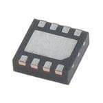
ICGOO电子元器件商城为您提供AD5116BCPZ80-500R7由Analog设计生产,在icgoo商城现货销售,并且可以通过原厂、代理商等渠道进行代购。 AD5116BCPZ80-500R7价格参考¥7.95-¥16.63。AnalogAD5116BCPZ80-500R7封装/规格:数据采集 - 数字电位器, Digital Potentiometer 80k Ohm 1 Circuit 64 Taps Pushbutton Interface 8-LFCSP-UD (2x2)。您可以下载AD5116BCPZ80-500R7参考资料、Datasheet数据手册功能说明书,资料中有AD5116BCPZ80-500R7 详细功能的应用电路图电压和使用方法及教程。
AD5116BCPZ80-500R7 是由 Analog Devices Inc.(现为 Analog Devices, Inc. 与 Linear Technology 合并后的一部分)生产的一款数字电位器,属于数据采集类产品。它具有非易失性存储功能,允许用户通过 SPI 接口编程设置电阻值,并在断电后保持设定值。以下是该型号的应用场景:

 1. 可调增益放大器
   - 在信号调理电路中,AD5116 可用于调整运算放大器的增益。通过改变反馈网络中的电阻值,可以动态调整放大器的增益,适用于需要灵活增益控制的系统。

 2. 电压基准调节
   - 数字电位器可以用作分压器来调节电压基准值。例如,在电源管理或数据采集系统中,可以根据需要动态调整参考电压,以适应不同的工作条件。

 3. 传感器校准
   - 在工业自动化、医疗设备或消费电子中,AD5116 可用于校准传感器输出。通过调整电位器的阻值,补偿传感器的偏移或灵敏度误差,实现精确测量。

 4. 音频音量控制
   - 在音频设备中,数字电位器可以用作音量控制器。相比传统的机械电位器,AD5116 提供了更高的可靠性和更小的体积,同时支持远程控制和自动调整。

 5. 电机控制
   - 在电机驱动电路中,AD5116 可用于调节电流限制或速度控制回路的参数。通过动态调整电阻值,优化电机性能并减少功耗。

 6. 电源管理
   - 在开关电源或线性稳压器中,AD5116 可用于调节输出电压或电流限制。这种非易失性数字电位器可以在系统启动时恢复到上次设定的参数,简化设计流程。

 7. 数据采集系统的信号调理
   - 在多通道数据采集系统中,AD5116 可用于匹配不同输入信号的范围。通过动态调整输入阻抗或增益,确保每个通道都能获得最佳的信号质量。

 特点总结:
- 非易失性存储:掉电后仍能保存设定值,无需重新配置。
- 小型封装:适合空间受限的设计。
- 高分辨率:提供精细的电阻调整能力。
- 低功耗:适用于电池供电设备。

这些特性使 AD5116 成为需要灵活、可靠电阻调整的应用的理想选择。
| 参数 | 数值 |
| 产品目录 | 集成电路 (IC)半导体 |
| 描述 | IC DGTL POT 64POS 80K 8LFCSP数字电位计 IC SGL CH64-Position I2C |
| DevelopmentKit | EVAL-AD5116EBZ |
| 产品分类 | |
| 品牌 | Analog Devices |
| 产品手册 | |
| 产品图片 |
|
| rohs | 符合RoHS无铅 / 符合限制有害物质指令(RoHS)规范要求 |
| 产品系列 | 数字电位计 IC,Analog Devices AD5116BCPZ80-500R7- |
| 数据手册 | |
| 产品型号 | AD5116BCPZ80-500R7 |
| PCN组件/产地 | |
| POT数量 | Single |
| 产品种类 | 数字电位计 IC |
| 供应商器件封装 | 8-LFCSP-UD(2x2) |
| 其它名称 | AD5116BCPZ80-500R7CT |
| 包装 | 剪切带 (CT) |
| 商标 | Analog Devices |
| 存储器类型 | 非易失 |
| 安装类型 | 表面贴装 |
| 安装风格 | SMD/SMT |
| 容差 | 8 % |
| 封装 | Reel |
| 封装/外壳 | 8-UFDFN 裸露焊盘,CSP |
| 封装/箱体 | LFCSP-8 |
| 工作温度 | -40°C ~ 125°C |
| 工作电源电压 | 5.5 V |
| 工厂包装数量 | 500 |
| 弧刷存储器 | Non Volatile |
| 抽头 | 64 |
| 接口 | 2 线按钮 |
| 数字接口 | Push Button |
| 最大工作温度 | + 125 C |
| 最小工作温度 | - 40 C |
| 标准包装 | 1 |
| 每POT分接头 | 64 |
| 温度系数 | 35 PPM / C |
| 电压-电源 | 2.3 V ~ 5.5 V |
| 电源电压-最大 | 5.5 V |
| 电源电压-最小 | 2.3 V |
| 电源电流 | 0.75 uA |
| 电路数 | 1 |
| 电阻 | 80 kOhms |
| 电阻(Ω) | 80k |
| 系列 | AD5116 |


- 商务部:美国ITC正式对集成电路等产品启动337调查
- 曝三星4nm工艺存在良率问题 高通将骁龙8 Gen1或转产台积电
- 太阳诱电将投资9.5亿元在常州建新厂生产MLCC 预计2023年完工
- 英特尔发布欧洲新工厂建设计划 深化IDM 2.0 战略
- 台积电先进制程称霸业界 有大客户加持明年业绩稳了
- 达到5530亿美元!SIA预计今年全球半导体销售额将创下新高
- 英特尔拟将自动驾驶子公司Mobileye上市 估值或超500亿美元
- 三星加码芯片和SET,合并消费电子和移动部门,撤换高东真等 CEO
- 三星电子宣布重大人事变动 还合并消费电子和移动部门
- 海关总署:前11个月进口集成电路产品价值2.52万亿元 增长14.8%


PDF Datasheet 数据手册内容提取
Single-Channel, 64-Position, Push Button, ±8% Resistor Tolerance, Nonvolatile Digital Potentiometer Data Sheet AD5116 FEATURES FUNCTIONAL BLOCK DIAGRAM Nominal resistor tolerance error: ±8% maximum VDD Wiper current: ±6 mA DATA Rheostat mode temperature coefficient: 35 ppm/°C EEPROM CONTROL Low power consumption: 2.5 µA max @ 2.7 V and 125°C LOGIC RDAC BLOCK DATA REGISTER Wide bandwidth: 4 MHz (5 kΩ option) VDD ASE Power-on EEPROM refresh time < 50 μs A PU 50-year typical data retention at 125°C ADAPTIVE W PD DEBOUNCER 1 million write cycles B 2B.u3i lVt- tino a5d.5a Vp tsiuvpe pdleyb oopuenrcaetrio n GND AD5116 09657-001 Wide operating temperature: −40°C to +125°C Figure 1. Thin, 2 mm × 2 mm × 0.55 mm 8-lead LFCSP package APPLICATIONS Table 1. NVM ±8% Resistance Tolerance Family Mechanical potentiometer replacement Model Resistance (kΩ) Position Interface Portable electronics level adjustment AD5110 10, 80 128 I2C Audio volume control AD5111 10, 80 128 Up/down Low resolution DAC AD5112 5, 10, 80 64 I2C LCD panel brightness and contrast control AD5113 5, 10, 80 64 Up/down Programmable voltage to current conversion Programmable filters, delays, time constants AD5116 5, 10, 80 64 Push button Feedback resistor programmable power supply AD5114 10, 80 32 I2C Sensor calibration AD5115 10, 80 32 Up/down GENERAL DESCRIPTION The AD5116 provides a nonvolatile digital potentiometer due to contact bounce (commonly found in mechanical solution for 64-position adjustment applications, offering switches). The debouncer is adaptive, accommodating a guaranteed low resistor tolerance errors of ±8% and up to variety of push buttons. ±6 mA current density in the A, B, and W pins. The low resistor The AD5116 can automatically save the last wiper position into tolerance, low nominal temperature coefficient, and high EEPROM, making it suitable for applications that require a bandwidth simplify open-loop applications, as well as tolerance power-up in the last wiper position, for example, audio matching applications. equipment. The new low A-W and B-W resistance feature minimizes The AD5116 is available in a 2 mm × 2 mm 8-lead LFCSP the wiper resistance in the extremes of the resistor array to package. The part is guaranteed to operate over the extended typically 45 Ω. industrial temperature range of −40°C to +125°C. A simple push button interface allows manual control with just two external push button switches. The AD5116 is designed with a built-in adaptive debouncer that ignores invalid bounces Rev. B Document Feedback Information furnished by Analog Devices is believed to be accurate and reliable. However, no responsibility is assumed by Analog Devices for its use, nor for any infringements of patents or other One Technology Way, P.O. Box 9106, Norwood, MA 02062-9106, U.S.A. rights of third parties that may result from its use. Specifications subject to change without notice. No license is granted by implication or otherwise under any patent or patent rights of Analog Devices. Tel: 781.329.4700 ©2011–2012 Analog Devices, Inc. All rights reserved. Trademarks and registered trademarks are the property of their respective owners. Technical Support www.analog.com
AD5116 Data Sheet TABLE OF CONTENTS Features .............................................................................................. 1 Test Circuits ..................................................................................... 12 Applications ....................................................................................... 1 Theory of Operation ...................................................................... 13 Functional Block Diagram .............................................................. 1 RDAC Register ............................................................................ 13 General Description ......................................................................... 1 EEPROM ..................................................................................... 13 Revision History ............................................................................... 2 Automatic Save Enable .............................................................. 13 Specifications ..................................................................................... 3 End Scale Resistance Indicator ................................................. 14 Electrical Characteristics ............................................................. 3 RDAC Architecture .................................................................... 14 Interface Timing Specifications .................................................. 5 Programming the Variable Resistor ......................................... 14 Timing Diagrams .......................................................................... 5 Programming the Potentiometer Divider ............................... 15 Absolute Maximum Ratings ............................................................ 6 Terminal Voltage Operating Range ......................................... 15 Thermal Resistance ...................................................................... 6 Power-Up Sequence ................................................................... 15 ESD Caution .................................................................................. 6 Layout and Power Supply Biasing ............................................ 15 Pin Configuration and Function Descriptions ............................. 7 Outline Dimensions ....................................................................... 16 Typical Performance Characteristics ............................................. 8 Ordering Guide .......................................................................... 16 REVISION HISTORY 11/12—Rev. A to Rev. B Changed Low Power Consumption from 2.5 mA to 2.5 µA....... 1 Changed I Unit from mA to µA, Table 2 .................................... 4 DD 4/12—Rev. 0 to Rev. A Changes to Features Section............................................................ 1 Changes to Positive Supply Current, Table 2 ................................ 4 Changes to Ordering Guide .......................................................... 16 10/11—Revision 0: Initial Version Rev. B | Page 2 of 16
Data Sheet AD5116 SPECIFICATIONS ELECTRICAL CHARACTERISTICS 5 kΩ, 10 kΩ, and 80 kΩ versions: V = 2.3 V to 5.5 V, V = V , V = 0 V, −40°C < T < +125°C, unless otherwise noted. DD A DD B A Table 2. Parameter Symbol Test Conditions/Comments Min Typ1 Max Unit DC CHARACTERISTICS—RHEOSTAT MODE Resolution N 6 Bits Resistor Integral Nonlinearity2 R-INL R = 5 kΩ, V = 2.3 V to 2.7 V −2.5 ±0.5 +2.5 LSB AB DD R = 5 kΩ, V = 2.7 V to 5.5 V −1 ±0.25 +1 LSB AB DD R = 10 kΩ −1 ±0.25 +1 LSB AB R = 80 kΩ −0.25 ±0.1 +0.25 LSB AB Resistor Differential Nonlinearity2 R-DNL −1 ±0.25 +1 LSB Nominal Resistor Tolerance ΔR /R −8 +8 % AB AB Resistance Temperature Coefficient3 (ΔR /R )/ΔT × 106 Code = full scale 35 ppm/°C AB AB Wiper Resistance R Code = zero scale 70 140 Ω W R Code = bottom scale 45 80 Ω BS R Code = top scale 70 140 Ω TS DC CHARACTERISTICS—POTENTIOMETER DIVIDER MODE Integral Nonlinearity4 INL −0.5 ±0.15 +0.5 LSB Differential Nonlinearity4 DNL −0.5 ±0.15 +0.5 LSB Full-Scale Error V R = 5 kΩ −2.5 LSB WFSE AB R =10 kΩ −1.5 LSB AB R = 80 kΩ −1 LSB AB Zero-Scale Error V R = 5 kΩ +1.5 LSB WZSE AB R =10 kΩ +1 LSB AB R = 80 kΩ +0.25 LSB AB Voltage Divider Temperature Coefficient3 (ΔV /V )/ΔT × 106 Code = half scale ±10 ppm/°C W W RESISTOR TERMINALS Maximum Continuous I, I, and I Current3 R = 5 kΩ, 10 kΩ −6 +6 mA A B W AB R = 80 kΩ −1.5 +1.5 mA AB Terminal Voltage Range5 GND V V DD Capacitance A, Capacitance B3, 6 C , C f = 1 MHz, measured to GND, 20 pF A B code = half scale, V = V = 2.5 V W A or V = V = 2.5 V W B Capacitance W3, 6 C f = 1 MHz, measured to GND, 35 pF W code = half scale, V = V = 2.5 V A B Common-Mode Leakage Current3 V = V = V 50 nA A W B DIGITAL INPUTS (PU AND PD) Input Logic3 High V 2 V INH Low V 0.8 V INL Input Current3 I ±1 µA N Input Capacitance3 C 5 pF IN DIGITAL OUTPUT (ASE) Output High Voltage3 V I = 2 mA, V = 5 V 4.8 V OH SINK DD Output Current3 I V = 5 V 16 mA O DD Three-State Leakage Current3 I ±1 µA OZ Input Capacitance3 C 5 pF IN Rev. B | Page 3 of 16
AD5116 Data Sheet Parameter Symbol Test Conditions/Comments Min Typ1 Max Unit POWER SUPPLIES Single-Supply Power Range 2.3 5.5 V Positive Supply Current I V = 5 V 0.75 3.5 µA DD DD V = 2.7 V 2.5 µA DD V = 2.3 V 2.4 µA DD EEMEM Store Current3, 7 I 2 mA DD_NVM_STORE EEMEM Read Current3, 8 I 320 µA DD_NVM_READ Power Dissipation9 P V = V or V = GND 5 µW DISS IH LOGIC IL Power Supply Rejection3 PSR ∆V /∆V = 5 V ± 10% DD SS R = 5 kΩ −43 dB AB R =10 kΩ −50 dB AB R = 80 kΩ −64 dB AB DYNAMIC CHARACTERISTICS3, 10 Bandwidth BW Code = half scale − 3 dB R = 5 kΩ 4 MHz AB R = 10 kΩ 2 MHz AB R = 80 kΩ 200 kHz AB Total Harmonic Distortion THD V = V /2 + 1 V rms, V = V /2, A DD B DD f = 1 kHz, code = half scale R = 5 kΩ −75 dB AB R = 10 kΩ −80 dB AB R = 80 kΩ −85 dB AB V Settling Time t V = 5 V, V = 0 V, ±0.5 LSB error W s A B band R = 5 kΩ 2.5 µs AB R = 10 kΩ 3 µs AB R = 80 kΩ 10 µs AB Resistor Noise Density e Code = half scale, T = 25°C, N_WB A f = 100 kHz R = 5 kΩ 7 nV/√Hz AB R = 10 kΩ 9 nV/√Hz AB R = 80 kΩ 20 nV/√Hz AB FLASH/EE MEMORY RELIABILITY3 Endurance11 T = 25°C 1 MCycles A 100 kCycles Data Retention12 50 Years 1 Typical values represent average readings at 25°C, VDD = 5 V, VSS = 0 V, and VLOGIC = 5 V. 2 Resistor position nonlinearity error (R-INL) is the deviation from an ideal value measured between the maximum resistance and the minimum resistance wiper positions. R-DNL measures the relative step change from ideal between successive tap positions. The maximum wiper current is limited to 0.8 × V /R . DD AB 3 Guaranteed by design and characterization, not subject to production test. 4 INL and DNL are measured at V with the RDAC configured as a potentiometer divider similar to a voltage output DAC. V = V and V = 0 V. DNL specification limits WB A DD B of ±1 LSB maximum are guaranteed monotonic operating conditions. 5 Resistor Terminal A, Resistor Terminal B, and Resistor Terminal W have no limitations on polarity with respect to each other. 6 C is measured with V = V = 2.5 V, C is measured with V = V = 2.5 V, and C is measured with V = V = 2.5 V. A W A B W B W A B 7 Different from operating current; supply current for NVM program lasts approximately 30 ms. 8 Different from operating current; supply current for NVM read lasts approximately 20 µs. 9 P is calculated from (I × V ). DISS DD DD 10 All dynamic characteristics use V = 5.5 V, and V = 5 V. DD LOGIC 11 Endurance is qualified at 100,000 cycles per JEDEC Standard 22, Method A117 and measured at 150°C. 12 Retention lifetime equivalent at junction temperature (T) = 125°C per JEDEC Standard 22, Method A117. Retention lifetime based on an activation energy of 1 eV J derates with junction temperature in the Flash/EE memory. Rev. B | Page 4 of 16
Data Sheet AD5116 INTERFACE TIMING SPECIFICATIONS V = 2.3 V to 5.5 V; all specifications T to T , unless otherwise noted. DD MIN MAX Table 3. Parameter Test Conditions/Comments Min Typ Max Unit Description t 8 ms Debounce time 1 t 1 sec Manual to auto scan time 2 t 140 ms Auto scan step 3 t ASE = 0 V, PD = GND, PU = GND 1 sec Auto save execute time 4 t ASE = V 8 ms Low pulse time to manual storage 5 DD t 1 15 50 ms Memory program time EEPROM_PROGRAM t 2 50 µs Power-on EEPROM restore time POWER_UP 1 EEPROM program time depends on the temperature and EEPROM write cycles. Higher timing is expected at a lower temperature and higher write cycles. 2 Maximum time after V is equal to 2.3 V. DD TIMING DIAGRAMS PD/PU (LOW) t1 t5 PtREEOPGRROAMM PU ASE PD (LOW) RW 09657-002 EEPROM DATA NEW DATA 09657-005 Figure 2. Manual Increment Mode Timing Figure 5. Manual Save Mode Timing t1 t1 t3 PD PU t2 RW= 45Ω PD (LOW) RW RW 09657-003 ASE 09657-006 Figure 3. Auto Increment Mode Timing Figure 6. End Scale Indication Timing t1 t4 PtREEOPGRROAMM PD RW ASE (LOW) EEPROM DATA NEW DATA 09657-004 Figure 4. Auto Save Mode Timing Rev. B | Page 5 of 16
AD5116 Data Sheet ABSOLUTE MAXIMUM RATINGS T = 25°C, unless otherwise noted. Stresses above those listed under Absolute Maximum Ratings A may cause permanent damage to the device. This is a stress Table 4. rating only; functional operation of the device at these or any Parameter Rating other conditions above those indicated in the operational V to GND –0.3 V to +7.0 V DD section of this specification is not implied. Exposure to absolute V , V , V to GND GND − 0.3 V to V + 0.3 V A W B DD maximum rating conditions for extended periods may affect I , I , I A W B device reliability. Pulsed1 Frequency > 10 kHz THERMAL RESISTANCE R = 5 kΩ and 10 kΩ ±6 mA/d2 AW θ is defined by JEDEC specification JESD-51, and the value is JA R = 80 kΩ ±1.5 mA/d2 AW dependent on the test board and test environment. Frequency ≤ 10 kHz R = 5 kΩ and 10 kΩ ±6 mA/√d2 Table 5. Thermal Resistance AW R = 80 kΩ ±1.5 mA/√d2 Package Type θ θ Unit AW JA JC Continuous 8-Lead LFCSP 901 25 °C/W R = 5 kΩ and 10 kΩ ±6mA AW R = 80 kΩ ±1.5mA 1 JEDEC 2S2P test board, still air (0 m/sec air flow). AW Push Button Inputs −0.3 V to +7 V or V + 0.3 V ESD CAUTION DD (whichever is less) Operating Temperature Range3 −40°C to +125°C Maximum Junction Temperature (T Max) 150°C J Storage Temperature Range −65°C to +150°C Reflow Soldering Peak Temperature 260°C Time At Peak Temperature 20 sec to 40 sec Package Power Dissipation (T max − T )/θ J A JA 1 Maximum terminal current is bounded by the maximum current handling of the switches, maximum power dissipation of the package, and maximum applied voltage across any two of the A, B, and W terminals at a given resistance. 2 Pulse duty factor. 3 Includes programming of EEPROM memory. Rev. B | Page 6 of 16
Data Sheet AD5116 PIN CONFIGURATION AND FUNCTION DESCRIPTIONS VDD 1 8 ASE A2 AD5116 7 PU TOP VIEW W3 (Not to Scale) 6 PD B4 5 GND N1 . O TFTHLEOES AETXIPNOGS.ED PAD IS INTERNALLY09657-007 Figure 7. Pin Configuration Table 6. Pin Function Descriptions Pin No. Mnemonic Description 1 V Positive Power Supply. This pin should be decoupled with 0.1μF ceramic capacitors and 10 μF capacitors. DD 2 A Terminal A of RDAC. GND ≤ V ≤ V . A DD 3 W Wiper terminal of RDAC. GND ≤ V ≤ V . W DD 4 B Terminal B of RDAC. GND ≤ V ≤ V . B DD 5 GND Ground Pin. 6 PD Push-Down Pin. Connect to the external push button. Active high. An internal 100 kΩ pull-down resistor is connected to GND. 7 PU Push-Up Pin. Connect to the external push button. Active high. An internal 100 kΩ pull-down resistor is connected to GND. 8 ASE Automatic Save Enable. Automatic save enable is configured at power-up. Active low. This pin requires a pull resistor connected between V or GND. If ASE is enabled, this pin also indicates when the end scale (maximum DD or minimum resistance) has been reached. EPAD Exposed Pad. The exposed pad is internally floating. Rev. B | Page 7 of 16
AD5116 Data Sheet TYPICAL PERFORMANCE CHARACTERISTICS 0.08 0.02 5kΩ, –40°C 5kΩ, +25°C 5kΩ, +125°C 0.01 0.06 0 0.04 –0.01 R-INL (LSB) 0.020 5kΩ, –40°C R-DNL (LSB)––00..0032 5kΩ, +25°C –0.04 –0.02 5kΩ, +125°C 10kΩ, –40°C 10kΩ, +25°C –0.05 –0.04 10kΩ, +125°C 80kΩ, –40°C –0.06 80kΩ, +25°C 10kΩ, –40°C 10kΩ, +25°C 10kΩ, +125°C 80kΩ, +125°C 80kΩ, –40°C 80kΩ, +25°C 80kΩ, +125°C –0.060 3 6 9 121518212C4O2D7E3 0(D3e3ci3m6a3l)94245485154576063 09657-008 –0.070 3 6 9 121518212C4O2D7E3 0(D3e3ci3m6a3l)94245485154576063 09657-011 Figure 8. R-INL vs. Code Figure 11. R-DNL vs. Code 0.08 0.02 5kΩ, –40°C 5kΩ, –40°C 5kΩ, +25°C 5kΩ, +125°C 5kΩ, +25°C 10kΩ, –40°C 10kΩ, +25°C 10kΩ, +125°C 0.06 5kΩ, +125°C 0.01 10kΩ, –40°C 10kΩ, +25°C 0.04 10kΩ, +125°C 0 80kΩ, –40°C 80kΩ, +25°C 0.02 80kΩ, +125°C –0.01 NL (LSB) 0 L (LSB)–0.02 I N –0.02 D–0.03 –0.04 –0.04 –0.06 –0.05 –0.080 3 6 9 121518212C4O2D7E3 (0D3e3cim36al3)94245485154576063 09657-009 –0.060 3 6809kΩ1,2 –4105°1C8212C84O02kD7ΩE,3 0(+D23e53c°Ci3m6a3l)98402k4Ω5, 4+812551°C54576063 09657-012 Figure 9. INL vs. Code Figure 12. DNL vs. Code 800 700 VVVDDDDDD===235..V33VV 1.2 TA = 25°C VVVDDDDDD === 253V..33VV 1.0 600 NT(nA) 500 T (mA) 0.8 E N R 400 E R R LYCU 300 Y CUR 0.6 P L UP 200 PP 0.4 S U S 100 0.2 0 –10–040 –25Fig–u1r0e 10.5 STuEpM2p0PlyE CRuA35rTrUeRnEt5 0v(°sC. T)6e5mpe8r0atur9e5 110 125 09657-010 00.05 0.65 1.25DIG1IT.8A5L IN2P.4U5T VO3L.0T5AGE3 (.6V5) 4.25 4.85 09657-013 Figure 13. Supply Current (I ) vs. Digital Input Voltage DD Rev. B | Page 8 of 16
Data Sheet AD5116 0 0 0x20 0x20 –10 0x10 –10 0x10 0x08 0x08 –20 –20 0x04 0x04 AIN (dB) –30 00xx0021 AIN (dB) –30 000xxx000210 G G –40 –40 0x00 –50 –50 –60 –6010k 100k FREQUE1NMCY (Hz) 10M 100M 09657-014 –7010k 100FkREQUENCY (Hz) 1M 10M 09657-017 Figure 14. 5 kΩ Gain vs. Frequency vs. Code Figure 17. 10 kΩ Gain vs. Frequency vs. Code 0 0 0x20 –10 0x10 –10 0x08 –20 0x04 –20 0x02 s) AIN (dB) ––4300 00xx0001 E (Degree ––4300 G AS –50 H –50 P –60 –60 RAB = 10kΩ –70 –70 FULL SCALE HALF SCALE QUARTER SCALE –8010k FREQU1E00NkCY(Hz) 1M 09657-015 –8010k 100kFREQUENCY (Hz)1M 10M 09657-018 Figure 15. 80 kΩ Gain vs. Frequency vs. Code Figure 18. Normalized Phase Flatness vs. Frequency m/°C)112680000 VDD185 =00k kkΩ5ΩΩV O (ppm/°C) 112680000 VDD185 =00k kkΩ5ΩΩV pp140 PC 140 CO (120 TEM 120 T MODE TEMP1068000 METER MODE 1680000 A O RHEOST 2400 POTENTI 2400 0 0 0 10 20 CODE3 0(Decimal4)0 50 60 09657-016 0 10 20 CODE3 0(Decimal4)0 50 60 09657-019 Figure 16. Rheostat Mode Tempco ΔRWB/ΔT vs. Code Figure 19. Potentiometer Mode Tempco ΔRWB/ΔT vs. Code Rev. B | Page 9 of 16
AD5116 Data Sheet 0 0 VDD = 5V 5kΩ 5kΩ VDD = 5V –10 VVAB == 22..55VV + 1VRMS 1800kkΩΩ –10 1800kkΩΩ VVAB == 22..55VV + VIN CODE = HALF SCALE fIN = 1kHz –20 NOISE FILTER = 22kHz –20 CODE = HALF SCALE NOISE FILTER = 22kHz –30 –30 N (dB) –40 N (dB) –40 THD + ––6500 THD + –50 –60 –70 –70 –80 –80 –90 –10020 200 FREQUE2NkCY (Hz) 20k 200k 09657-020 –900.001 0.01AMPLITUDE (V r0m.1s) 1 09657-023 Figure 20. Total Harmonic Distortion + Noise (THD + N) vs. Frequency Figure 23. Total Harmonic Distortion + Noise (THD + N) vs. Amplitude 80 0.35 5k + 250pF 80k + 150pF VDD = 5V 70 111000kkk +++ 712555p00ppFFF 8550kkk ++ + 07 2p55pF0FpF 0.30 VVBA == GVNDDD 80k + 0pF 5k + 150pF 0.25 5kΩ H (MHz) 5600 80k + 75pF 10k + 0pF LTAGE (V)00..1250 1800kkΩΩ T O D 40 V ANDWI 30 ATIVE 0.10 B L0.05 E R 20 0 10 –0.05 00 10 20 CODE30 (Decima4l)0 50 60 09657-021 –0.10–1 1 3 TIME (µ5s) 7 9 09657-024 Figure 21. Maximum Bandwidth vs. Code vs. Net Capacitance Figure 24. Maximum Transition Glitch 150 0.0025 1.2 Ω) TA = 25°C 5.5V E ( 5V C 3.3V N 2.7V 1.0 ON RESISTA12900 2.3V DENSITY 00..00001250 0.8 OBABILITY CREMENTAL WIPER 3600 PROBABILITY 00..00000150 000...246 CUMULATIVE PR N I 00 1 2 VDD3 (V) 4 5 6 09657-022 0–600 –500 –400 –300 –R2E00SIS–1T0O0R D0RIF1T0 0(pp2m00) 300 400 500 6000 09657-047 Figure 22. Incremental Wiper on Resistance vs. V Figure 25. Resistor Lifetime Drift DD Rev. B | Page 10 of 16
Data Sheet AD5116 0 –10 VVVHDABAD L== F =4G SV5NVCD A±L 1E0% AC 518k00kkΩΩΩ 67 18500kkkΩΩΩ TA = 25°C –20 mA) 5 RR (dB) –30 AL I (MAX 4 PS –40 ETIC 3 R O –50 E H 2 T –60 1 –70 10 100 F1RkEQUENCY1 (0Hkz) 100k 1M 09657-026 00 10 20 CODE3 0(Decimal4)0 50 60 09657-029 Figure 26. Power Supply Rejection Ratio (PSRR) vs. Frequency Figure 29. Theoretical Maximum Current vs. Code 0.4 20 0.3 VVDAD = =V 5DVD 18 TA = 25°C VB = GND 16 0.2 14 V) 0.1 A) m m 12 VOLTAGE ( –0.10 CURRENT ( 108 –0.2 6 –0.3 4 –0.4 10kΩ 2 80kΩ –0.50 5kΩ 0.6 TIM1E.2 (µs) 1.8 2.5 09657-027 00 1 2 VDD (V3) 4 5 09657-044 Figure 27. Digital Feedthrough Figure 30. Maximum ASE Output Current vs. Voltage 0 8 51k0kΩΩ VDD = 3V 80kΩ 7 –10 6 –20 A) 5 m N (dB) –30 ENT ( 4 GAI –40 URR C 3 –50 2 –60 1 –701k 10kFREQUENCY (Hz) 1M 10M 09657-028 0–40 –20 0 T2E0MPER4A0TURE6 (0°C) 80 100 120 09657-045 Figure 28. Shutdown Isolation vs. Frequency Figure 31. Maximum ASE Output Current vs. Temperature Rev. B | Page 11 of 16
AD5116 Data Sheet TEST CIRCUITS Figure 32 to Figure 37 define the test conditions used in the Specifications section. NC DUT A IW VA W V+=VDD±10% B NC = NO CVOMNSNECT 09657-030 V+ ~ VDD BA W VMS PPSSSRR(%(d/%B))==ΔΔ20VV MDloDSg%%ΔΔVVMDDS 09657-033 Figure 32. Resistor Position Nonlinearity Error Figure 35. Power Supply Sensitivity (PSS, PSRR) (Rheostat Operation: R-INL, R-DNL) A +15V DUT V+=VDD W A 1LSB=V+/2N VIN DUT V+ W OFFSET B OP42 VOUT B GND VMS 09657-031 2.5V –15V 09657-034 Figure 33. Potentiometer Divider Nonlinearity Error (INL, DNL) Figure 36. Gain and Phase vs. Frequency VDD GND NC 0.1V DUT RW= IWB GND A W + VDD DUT A W ICM B IWB –0.1V GND B NC=NOCONNECTGND TOVDD 09657-032 VDD GND VDD 09657-035 Figure 34. Wiper Resistance Figure 37. Common-Mode Leakage Current Rev. B | Page 12 of 16
Data Sheet AD5116 THEORY OF OPERATION The AD5116 digital programmable resistor is designed to steps are not equal to 1 LSB, and are not included in the INL, operate as a true variable resistor for analog signals within DNL, R-INL, and R-DNL specifications. the terminal voltage range of GND < V < V . The resistor TERM DD Whenever the minimum R (= R ) is reached, the resistance WB BS wiper position is determined by the RDAC register contents. stops decrementing. Any continuous holding of the PD to logic The RDAC register is a standard logic register; there is no high simply elevates the supply current. When R reaches the AW restriction on the number of changes allowed. minimum resistance (= R ), continuous holding of PU only TS The RDAC register can be programmed with any position elevates the supply current. setting using the push button interface. Once a desirable wiper EEPROM position is found, this value can be stored in the EEPROM The AD5116 contains an EEPROM memory that allows memory. Thereafter, the wiper position is always restored to wiper position storage. Once a desirable wiper position is that position for subsequent power-up. The storing of EEPROM found, this value can be saved into the EEPROM. Thereafter, data takes approximately 20 ms; during this time, the device the wiper position will always be set at that position for any is locked and does not accept any new operation, thus future on-off-on power supply sequence. preventing any changes from taking place. AUTOMATIC SAVE ENABLE The AD5116 is designed to support external push buttons (tactile switches) directly, as shown in Figure 1. At power-up, the AD5116 checks the level in the ASE pin. If the RDAC REGISTER pin is pulled low, as shown in Figure 38, the automatic store is enabled. If the pin is pulled high, as shown in Figure 39, The RDAC register directly controls the position of the digital automatic store is disabled and the RDAC register should be potentiometer wiper. For example, when the RDAC register stored manually. During the storage cycle, the device is locked is 0x20, the wiper is connected to midscale of the variable and does not accept any new operation preventing any changes resistor. The RDAC register is controlled using the PD and PU from taking place. push buttons. The step-up and step-down operations require the activation of the PU (push-up) and PD (push-down) pins. ASE These pins have 100 kΩ internal pull-up resistors that PU and AD5116 PD activate at logic high. The following paragraphs explain how 100kΩ GND tvoa liindc troe mdeecnrte tmhee nRtD thAeC R rDeAgiCst erre,g bisutte ar,l ls wthaep dpeinscgr PipUti obnys P aDre. 09657-036 Manual Increment Figure 38. Automatic Store Enables The AD5116 features an adaptive debouncer that monitors the Auto Save duration of the logic high level of PU signal between bounces. If If there is no activity on inputs during 1 second, the AD5116 the PU logic high level signal duration is shorter than 8 ms, the stores the RDAC register data into EEPROM, as shown in debouncer ignores it as an invalid incrementing command. Figure 4. Whenever the logic high level of PU signal lasts longer than Manual Store 8 ms, the debouncer assumes that the last bounce is met and, therefore, increments the RDAC register by one step. The wiper The storage is controlled by the ASE pin, which is connected to is incremented by one tap position, as shown in Figure 2. an adaptive debouncer. If the ASE pin is pulled low longer than 8 ms, the AD5116 saves the RDAC register data into EEPROM, Auto Scan Increment as shown in Figure 5. If the PU button is held for longer than 1 second, continuously VDD holding it activates auto scan mode, and the AD5116 increments the RDAC register by one step every 140 ms until PU is released. Typical timing is shown in Figure 3. 100kΩ VDD Low Wiper Resistance Feature ASE AD5116 rTehsies tAaDnc5e1. 1B6e itnwceleund eTse ermxtrina aslt eWps a tnod a Tcheriemvien aa lm Bi,n tihmisu emxt wrai pseterp 09657-037 is called bottom scale and the wiper resistance decreases from Figure 39. Automatic Store Disables with Manual Storage Push Button 70 Ω to 45 Ω. Between Terminal A and Terminal W, this extra step is called top scale and connects the A and W terminals, reducing the 1 LSB resistor typical at full-scale code. These new extra steps are loaded automatically in the RDAC register after zero-scale or full-scale position has been reached. The extra Rev. B | Page 13 of 16
AD5116 Data Sheet END SCALE RESISTANCE INDICATOR steps are not equal to 1 LSB and are not included in the INL, DNL, R-INL, and R-DNL specifications. When the auto save mode is enabled, the ASE pin also indicates when the RDAC register reaches the maximum or minimum PROGRAMMING THE VARIABLE RESISTOR scale. The AD5116 pulls the ASE pin high and holds it as long Rheostat Operation—±8% Resistor Tolerance as PD or PU is active, and the part is placed in the end scale The AD5116 operates in rheostat mode when only two terminals resistance (R or R ), as shown in Figure 6. The typical pin TS BS are used as a variable resistor. The unused terminal can be configuration is shown in Figure 40. floating or tied to the W terminal as shown in Figure 42. When the part is placed at the end of the resistance scale (R or TS A A A R ), the ASE pin is pulled high during the debounce time, until BS W W W the RDAC register is incremented (R ) or decremented (R ) by activating PU or PD. BS TS B B B 09657-040 Figure 42. Rheostat Mode Configuration ASE AD5116 The nominal resistance between Terminal A and Terminal B, 100kΩ GND RAB, is available in 5 kΩ, 10 kΩ, and 80 kΩ and has 64 tap points 09657-038 laactccehs sise dd ebcyo tdheed w toip seerl etecrt moninea ol.f Tthhee 664- bpiot sdsaibtale i nw tipheer R sDetAtiCng s. Figure 40. Typical End Scale Indicator Circuit The general equation for determining the digitally programmed RDAC ARCHITECTURE output resistance between the W terminal and B terminal is: To achieve optimum performance, Analog Devices, Inc., has RWB =RBS Bottom scale (1) patented the RDAC segmentation architecture for all the digital D R (D)= ×R +R From 0 to 64 (2) potentiometers. In particular, the AD5116 employs a two-stage WB 64 AB W segmentation approach as shown in Figure 41. The AD5116 where: wiper switch is designed with the transmission gate CMOS D is the decimal equivalent of the binary code in the 6-bit topology and with the gate voltage derived from V . DD RDAC register. A TS RAB is the end-to-end resistance. R is the wiper resistance at bottom scale. BS RL Similar to the mechanical potentiometer, the resistance of the RDAC between the W terminal and the A terminal also RL SW produces a digitally controlled complementary resistance, RWA. R starts at the maximum resistance value and decreases as the RW WA data loaded into the latch increases. The general equation for W this operation is: 6-BIT RW R =R +R Bottom scale (3) DAEDCDORDESESR RL AW AB W 64−D R (D)= ×R +R From 0 to 63 (4) AW 64 AB W RL BS R =R Top scale (5) AW TS where: B D is the decimal equivalent of the binary code in the 6-bit 09657-039 RRDA isC t hreeg einstde-rt. o-end resistance. AB Figure 41. Simplified RDAC Circuit R is the wiper resistance. W Top Scale/Bottom Scale Architecture R is the wiper resistance at top scale. TS In addition, the AD5116 includes a new feature to reduce the Regardless of which setting the part is operating in, take care resistance between terminals. These extra steps are called to limit the current between the A terminal to B terminal, W bottom scale and top scale. At bottom scale, the typical wiper terminal to A terminal, and W terminal to B terminal, to the resistance decreases from 70 Ω to 45 Ω. At top scale, the maximum continuous current or pulsed current specified in resistance between Terminal A and Terminal W is decreased Table 4. Otherwise, degradation or possible destruction of by 1 LSB and the total resistance is reduced to 70 Ω. The extra the internal switch contact can occur. Rev. B | Page 14 of 16
Data Sheet AD5116 PROGRAMMING THE POTENTIOMETER DIVIDER any voltage to Terminal A, Terminal B, and Terminal W. Voltage Output Operation Otherwise, the diodes are forward-biased such that VDD is powered on unintentionally and can affect other parts of the The digital potentiometer easily generates a voltage divider at circuit. Similarly, V should be powered down last. The ideal wiper-to-B and wiper-to-A that is proportional to the input DD power-on sequence is in the following order: GND, V , and voltage at A to B, as shown in Figure 43. Unlike the polarity of DD V /V /V . The order of powering V , V , and V is not V to GND, which must be positive, voltage across A-to-B, W- A B W A B W DD important as long as they are powered on after V . The to-A, and W-to-B can be at either polarity. DD states of the PU and PD pins can be logic low or floating, VIN but they should not be logic high during power-on. A W VOUT VDD B 09657-041 A Figure 43. Potentiometer Mode Configuration W If ignoring the effect of the wiper resistance for simplicity, connecting Terminal A to 5 V and Terminal B to ground B produces an output voltage at the Wiper W to Terminal B roauntpgiuntg v forlotamge 0 a Vt V toW ,5 w Vi.t hT hrees gpeencet rtaol gerqouuantido nfo dr eafninyi vnagl itdh e GND 09657-042 input voltage applied to Terminal A and Terminal B, is: Figure 44. Maximum Terminal Voltages Set by V and V DD SS R (D) R (D) LAYOUT AND POWER SUPPLY BIASING V (D)= WB ×V + AW ×V (6) W R A R B AB AB It is always a good practice to use compact, minimum lead length layout design. The leads to the input should be as direct where: as possible with a minimum conductor length. Ground paths R (D) can be obtained from Equation 1 or Equation 2. WB should have low resistance and low inductance. It is also good R (D) can be obtained from Equation 3 to Equation 5 . AW practice to bypass the power supplies with quality capacitors. Operation of the digital potentiometer in the divider mode Low equivalent series resistance (ESR) 1 μF to 10 μF tantalum results in a more accurate operation over temperature. Unlike or electrolytic capacitors should be applied at the supplies to the rheostat mode, the output voltage is dependent mainly minimize any transient disturbance and to filter low frequency on the ratio of the internal resistors, R and R , and not the WA WB ripple. Figure 45 illustrates the basic supply bypassing config- absolute values. Therefore, the temperature drift reduces to uration for the AD5116. 5 ppm/°C. TERMINAL VOLTAGE OPERATING RANGE AD5116 The AD5116 is designed with internal ESD diodes for VDD VDD C2+ C1 protection. These diodes also set the voltage boundary of 10µF 0.1µF GND tTheer mteirnmali nAa,l Toepremraitnianlg B v,o oltra Tgeersm. Pionsailt iWve tshigant aelxsc peereds VenDtD o anre AGND 09657-043 clamped by the forward-biased diode. There is no polarity Figure 45. Power Supply Bypassing constraint between V , V , and V , but they cannot be higher A W B than V or lower than GND. DD POWER-UP SEQUENCE Because of the ESD protection diodes that limit the voltage compliance at Terminal A, Terminal B, and Terminal W (see Figure 44), it is important to power on V before applying DD Rev. B | Page 15 of 16
AD5116 Data Sheet OUTLINE DIMENSIONS 1.70 1.60 2.00 1.50 BSC SQ 0.50 BSC 5 8 0.175 REF PIN 1 INDEX EXPOSED 1.10 AREA PAD 1.00 0.425 0.90 0.350 0.275 4 1 PIN 1 TOP VIEW BOTTOM VIEW INDICATOR (R 0.15) 0.60 FOR PROPER CONNECTION OF 0.55 0.05 MAX THE EXPOSED PAD, REFER TO THE PIN CONFIGURATION AND 0.50 0.02 NOM FUNCTION DESCRIPTIONS SECTION OF THIS DATA SHEET. SEPALTAINNGE 000...322050 0.20 REF 07-11-2011-B Figure 46. 8-Lead Lead Frame Chip Scale Package [LFCSP_UD] 2.00 mm × 2.00 mm Body, Ultra Thin, Dual Lead (CP-8-10) Dimensions shown in millimeters ORDERING GUIDE Model1, 2 R (kΩ) Resolution Temperature Range Package Description Package Option Branding Code AB AD5116BCPZ5-RL7 5 64 −40°C to +125°C 8-Lead LFCSP_UD CP-8-10 7G AD5116BCPZ5-500R7 5 64 −40°C to +125°C 8-Lead LFCSP_UD CP-8-10 7G AD5116BCPZ10-RL7 10 64 −40°C to +125°C 8-Lead LFCSP_UD CP-8-10 7F AD5116BCPZ10-500R7 10 64 −40°C to +125°C 8-Lead LFCSP_UD CP-8-10 7F AD5116BCPZ80-RL7 80 64 −40°C to +125°C 8-Lead LFCSP_UD CP-8-10 7H AD5116BCPZ80-500R7 80 64 −40°C to +125°C 8-Lead LFCSP_UD CP-8-10 7H EVAL-AD5116EBZ Evaluation Board 1 Z = RoHS Compliant Part. 2 The EVAL-AD5116EBZ has an R of 10 kΩ. AB ©2011–2012 Analog Devices, Inc. All rights reserved. Trademarks and registered trademarks are the property of their respective owners. D09657-0-11/12(B) Rev. B | Page 16 of 16
Mouser Electronics Authorized Distributor Click to View Pricing, Inventory, Delivery & Lifecycle Information: A nalog Devices Inc.: AD5116BCPZ10-RL7 AD5116BCPZ5-RL7 AD5116BCPZ10-500R7 AD5116BCPZ80-500R7 AD5116BCPZ5-500R7 AD5116BCPZ80-RL7 EVAL-AD5116EBZ