ICGOO在线商城 > 集成电路(IC) > 数据采集 - 数字电位器 > AD5110BCPZ80-500R7
 Datasheet下载
- 型号: AD5110BCPZ80-500R7
- 制造商: Analog
- 库位|库存: xxxx|xxxx
- 要求:
| 数量阶梯 | 香港交货 | 国内含税 |
| +xxxx | $xxxx | ¥xxxx |
查看当月历史价格
查看今年历史价格
AD5110BCPZ80-500R7产品简介:
ICGOO电子元器件商城为您提供AD5110BCPZ80-500R7由Analog设计生产,在icgoo商城现货销售,并且可以通过原厂、代理商等渠道进行代购。 AD5110BCPZ80-500R7价格参考。AnalogAD5110BCPZ80-500R7封装/规格:数据采集 - 数字电位器, Digital Potentiometer 80k Ohm 1 Circuit 128 Taps I²C Interface 8-LFCSP-UD (2x2)。您可以下载AD5110BCPZ80-500R7参考资料、Datasheet数据手册功能说明书,资料中有AD5110BCPZ80-500R7 详细功能的应用电路图电压和使用方法及教程。
AD5110BCPZ80-500R7 是由 Analog Devices Inc. 生产的一款数字电位器,广泛应用于需要精确电阻调节的场景。以下是其主要应用场景:

 1. 自动增益控制 (AGC)
在通信和音频设备中,AD5110BCPZ80-500R7 可用于实现自动增益控制。通过调整电位器的阻值,可以动态地改变信号放大倍数,确保输出信号的稳定性和一致性。例如,在无线接收器中,可以根据接收到的信号强度自动调整增益,避免过载或信号丢失。

 2. 传感器校准
在工业自动化和医疗设备中,传感器的精度至关重要。AD5110BCPZ80-500R7 可以用于传感器的校准过程中,通过调整电位器的阻值来微调传感器的输出,确保测量结果的准确性。例如,在温度、压力或湿度传感器中,使用该电位器可以补偿环境变化对传感器的影响。

 3. 电源管理
在电源管理系统中,AD5110BCPZ80-500R7 可以用于调节电压或电流设置点。例如,在可调稳压电源中,通过改变电位器的阻值,可以精确控制输出电压的大小,满足不同负载的需求。此外,它还可以用于电池充电电路中,调节充电电流或电压,确保电池的安全和寿命。

 4. 滤波器调节
在模拟滤波器设计中,AD5110BCPZ80-500R7 可以用于调节滤波器的截止频率或品质因数(Q值)。通过编程改变电位器的阻值,可以动态调整滤波器的特性,适应不同的信号处理需求。例如,在音频处理设备中,可以根据用户需求调整低通或高通滤波器的频率响应。

 5. 测试与测量设备
在精密测试仪器中,AD5110BCPZ80-500R7 可用于校准和调节测量参数。例如,在万用表或示波器中,可以通过电位器调整参考电压或灵敏度,确保测量结果的准确性和稳定性。

 6. 电机控制
在电机控制系统中,AD5110BCPZ80-500R7 可以用于调节电机的速度或转矩。通过改变电位器的阻值,可以动态调整电机驱动电路中的电流或电压,从而实现对电机运行状态的精确控制。

总之,AD5110BCPZ80-500R7 数字电位器凭借其高精度、可编程性和可靠性,适用于多种需要精确电阻调节的应用场景,特别是在要求高稳定性和灵活性的系统中表现尤为出色。
| 参数 | 数值 |
| 产品目录 | 集成电路 (IC)半导体 |
| 描述 | IC DGTL POT 128POS 80K 8LFCSP数字电位计 IC SGL CH128-Position I2C |
| 产品分类 | |
| 品牌 | Analog Devices |
| 产品手册 | |
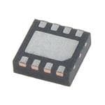
| 产品图片 |
|
| rohs | 符合RoHS无铅 / 符合限制有害物质指令(RoHS)规范要求 |
| 产品系列 | 数字电位计 IC,Analog Devices AD5110BCPZ80-500R7- |
| 数据手册 | |
| 产品型号 | AD5110BCPZ80-500R7 |
| PCN组件/产地 | 点击此处下载产品Datasheet点击此处下载产品Datasheet点击此处下载产品Datasheet点击此处下载产品Datasheet |
| POT数量 | Single |
| 产品种类 | 数字电位计 IC |
| 供应商器件封装 | 8-LFCSP-UD(2x2) |
| 其它名称 | AD5110BCPZ80-500R7DKR |
| 包装 | Digi-Reel® |
| 商标 | Analog Devices |
| 存储器类型 | 非易失 |
| 安装类型 | 表面贴装 |
| 安装风格 | SMD/SMT |
| 容差 | 8 % |
| 封装 | Reel |
| 封装/外壳 | 8-UFDFN 裸露焊盘,CSP |
| 封装/箱体 | LFCSP-8 |
| 工作温度 | -40°C ~ 125°C |
| 工作电源电压 | 5.5 V |
| 工厂包装数量 | 500 |
| 弧刷存储器 | Non Volatile |
| 抽头 | 128 |
| 接口 | I²C,2 线串口 |
| 数字接口 | I2C |
| 最大工作温度 | + 125 C |
| 最小工作温度 | - 40 C |
| 标准包装 | 1 |
| 每POT分接头 | 128 |
| 温度系数 | 35 PPM / C |
| 电压-电源 | 1.8 V ~ 5 V,2.3 V ~ 5.5V |
| 电源电压-最大 | 5.5 V |
| 电源电压-最小 | 2.3 V |
| 电源电流 | 0.75 uA |
| 电路数 | 1 |
| 电阻 | 80 kOhms |
| 电阻(Ω) | 80k |
| 系列 | AD5110 |
| 缓冲刷 | Non Buffered |


- 商务部:美国ITC正式对集成电路等产品启动337调查
- 曝三星4nm工艺存在良率问题 高通将骁龙8 Gen1或转产台积电
- 太阳诱电将投资9.5亿元在常州建新厂生产MLCC 预计2023年完工
- 英特尔发布欧洲新工厂建设计划 深化IDM 2.0 战略
- 台积电先进制程称霸业界 有大客户加持明年业绩稳了
- 达到5530亿美元!SIA预计今年全球半导体销售额将创下新高
- 英特尔拟将自动驾驶子公司Mobileye上市 估值或超500亿美元
- 三星加码芯片和SET,合并消费电子和移动部门,撤换高东真等 CEO
- 三星电子宣布重大人事变动 还合并消费电子和移动部门
- 海关总署:前11个月进口集成电路产品价值2.52万亿元 增长14.8%


PDF Datasheet 数据手册内容提取
Single-Channel, 128-/64-/32-Position, I2C, ±8% Resistor Tolerance, Nonvolatile Digital Potentiometer Data Sheet AD5110/AD5112/AD5114 FEATURES FUNCTIONAL BLOCK DIAGRAM Nominal resistor tolerance error: ±8% maximum VLOGIC VDD Wiper current: ±6 mA AD5110/AD5112/AD5114 Rheostat mode temperature coefficient: 35 ppm/°C POWER-ON Low power consumption: 2.5 µA max @ 2.7 V and 125°C RESET A Wide bandwidth: 4 MHz (5 kΩ option) W Power-on EEPROM refresh time < 50 μs DATA 50-year typical data retention at 125°C SDA EEPROM B I2C 1 million write cycles SERIAL 2.3 V to 5.5 V analog supply operation SCL INTERFACE DATA RERGDISATCER 1.8 V to 5.5 V logic supply operation WThiidne, 2o pmemra t×in 2g m temm ×p 0er.5a5tu mrem: − 84-0le°aCd t oL F+C1S2P5 °pCa ckage GND 09582-001 Figure 1. APPLICATIONS Mechanical potentiometer replacement Portable electronics level adjustment Table 1. ±8% Resistance Tolerance Family Audio volume control Model Resistance (kΩ) Position Interface Low resolution DAC AD5110 10, 80 128 I2C LCD panel brightness and contrast control AD5111 10, 80 128 Up/down Programmable voltage to current conversion AD5112 5, 10, 80 64 I2C Programmable filters, delays, time constants AD5113 5, 10, 80 64 Up/down Feedback resistor programmable power supply AD5116 5, 10, 80 64 Push-button Sensor calibration AD5114 10, 80 32 I2C AD5115 10, 80 32 Up/down GENERAL DESCRIPTION The AD5110/AD5112/AD5114 provide a nonvolatile solution The wiper settings are controllable through an I2C-compatible for 128-/64-/32-position adjustment applications, offering digital interface that is also used to readback the wiper register guaranteed low resistor tolerance errors of ±8% and up to and EEPROM content. Resistor tolerance is stored within ±6 mA current density in the A, B, and W pins. The low resistor EEPROM, providing an end-to-end tolerance accuracy of 0.1%. tolerance, low nominal temperature coefficient and high The AD5110/AD5112/AD5114 are available in a 2 mm × 2 mm bandwidth simplify open-loop applications, as well as tolerance LFCSP package. The parts are guaranteed to operate over the matching applications. extended industrial temperature range of −40°C to +125°C. The new low wiper resistance feature minimizes the wiper resistance in the extremes of the resistor array to only 45 Ω, typical. Rev. B Document Feedback Information furnished by Analog Devices is believed to be accurate and reliable. However, no responsibility is assumed by Analog Devices for its use, nor for any infringements of patents or other One Technology Way, P.O. Box 9106, Norwood, MA 02062-9106, U.S.A. rights of third parties that may result from its use. Specifications subject to change without notice. No license is granted by implication or otherwise under any patent or patent rights of Analog Devices. Tel: 781.329.4700 ©2011–2012 Analog Devices, Inc. All rights reserved. Trademarks and registered trademarks are the property of their respective owners. Technical Support www.analog.com
AD5110/AD5112/AD5114 Data Sheet TABLE OF CONTENTS Features .............................................................................................. 1 Theory of Operation ...................................................................... 19 Applications ....................................................................................... 1 RDAC Register and EEPROM .................................................. 19 Functional Block Diagram .............................................................. 1 I2C Serial Data Interface ............................................................ 19 General Description ......................................................................... 1 Input Shift Register .................................................................... 20 Revision History ............................................................................... 2 Write Operation.......................................................................... 21 Specifications ..................................................................................... 3 EEPROM Write Acknowlegde Polling .................................... 23 Electrical Characteristics—AD5110 .......................................... 3 Read Operation........................................................................... 23 Electrical Characteristics—AD5112 .......................................... 5 Reset ............................................................................................. 23 Electrical Characteristics—AD5114 .......................................... 7 Shutdown Mode ......................................................................... 23 Interface Timing Specifications .................................................. 9 RDAC Architecture .................................................................... 24 Shift Register and Timing Diagram ......................................... 10 Programming the Variable Resistor ......................................... 24 Absolute Maximum Ratings .......................................................... 11 Programming the Potentiometer Divider ............................... 25 Thermal Resistance .................................................................... 11 Terminal Voltage Operating Range ......................................... 26 ESD Caution ................................................................................ 11 Power-Up Sequence ................................................................... 26 Pin Configuration and Function Descriptions ........................... 12 Layout and Power Supply Biasing ............................................ 26 Typical Performance Characteristics ........................................... 13 Outline Dimensions ....................................................................... 27 Test Circuits ..................................................................................... 18 Ordering Guide .......................................................................... 27 REVISION HISTORY 11/12—Rev. A to Rev. B Changed Low Power Consumption from 2.5 mA to 2.5 µA....... 1 Changed I Unit from mA to µA, Table 2 .................................... 4 DD Changed I Unit from mA to µA, Table 3 .................................... 6 DD Changed I Unit from mA to µA, Table 4 .................................... 8 DD Changes to Figure 45 ...................................................................... 23 4/12—Rev. 0 to Rev. A Changes to Features Section............................................................ 1 Changes to Positive Supply Current, Table 2 ................................ 4 Changes to Positive Supply Current, Table 3 ................................ 6 Changes to Positive Supply Current, Table 4 ................................ 8 Updated Outline Dimensions ....................................................... 27 10/11—Revision 0: Initial Version Rev. B | Page 2 of 28
Data Sheet AD5110/AD5112/AD5114 SPECIFICATIONS ELECTRICAL CHARACTERISTICS—AD5110 10 kΩ and 80 kΩ versions: V = 2.3 V to 5.5 V, V = 1.8 V to V , V = V , V = 0 V, −40°C < T < +125°C, unless otherwise noted. DD LOGIC DD A DD B A Table 2. Parameter Symbol Test Conditions/Comments Min Typ1 Max Unit DC CHARACTERISTICS—RHEOSTAT MODE Resolution N 7 Bits Resistor Integral Nonlinearity2 R-INL R = 10 kΩ, V = 2.3 V to 2.7 V −2.5 ±0.5 +2.5 LSB AB DD R = 10 kΩ, V = 2.7 V to 5.5 V −1 ±0.25 +1 LSB AB DD R = 80 kΩ −0.5 ±0.1 +0.5 LSB AB Resistor Differential Nonlinearity2 R-DNL −1 ±0.25 +1 LSB Nominal Resistor Tolerance ΔR /R −8 +8 % AB AB Resistance Temperature Coefficient3 (ΔR /R )/ΔT × 106 Code = full scale 35 ppm/°C AB AB Wiper Resistance R Code = zero scale 70 140 Ω W R Code = bottom scale 45 80 Ω BS R Code = top scale 70 140 Ω TS DC CHARACTERISTICS—POTENTIOMETER DIVIDER MODE Integral Nonlinearity4 INL −0.5 ±0.15 +0.5 LSB Differential Nonlinearity4 DNL −0.5 ±0.15 +0.5 LSB Full-Scale Error V R = 10 kΩ −2.5 LSB WFSE AB R = 80 kΩ −1.5 LSB AB Zero-Scale Error V R = 10 kΩ 1.5 LSB WZSE AB R = 80 kΩ 0.5 LSB AB Voltage Divider Temperature Coefficient3 (ΔV /V )/ΔT × 106 Code = half scale ±10 ppm/°C W W RESISTOR TERMINALS Maximum Continuous I , I, and I R = 10 kΩ −6 +6 mA A B W AB Current3 R = 80 kΩ −1.5 +1.5 mA AB Terminal Voltage Range5 GND V V DD Capacitance A, Capacitance B3 C , C f = 1 MHz, measured to GND, 20 pF A B code = half scale, V = V = 2.5 V or V = V = 2.5 V W A W B Capacitance W3 C f = 1 MHz, measured to GND, 35 pF W code = half scale, V = V = 2.5 V A B Common-Mode Leakage Current3 V = V = V −500 ±15 +500 nA A W B DIGITAL INPUTS Input Logic3 High V V = 1.8 V to 2.3 V 0.8 × V V INH LOGIC LOGIC V = 2.3 V to 5.5 V 0.7 × V V LOGIC LOGIC Low V V = 1.8 V to 2.3 V 0.2 × V V INL LOGIC LOGIC V = 2.3 V to 5.5 V 0.3 × V V LOGIC LOGIC Input Hysteresis3 V 0.1 × V V HYST LOGIC Input Current3 I ±1 µA N Input Capacitance3 C 5 pF IN DIGITAL OUTPUT (SDA) Output Low Voltage3 V I = 3 mA 0.2 V OL SINK I = 6 mA 0.4 V SINK Three-State Leakage Current −1 +1 µA Three-State Output Capacitance3 2 pF Rev. B | Page 3 of 28
AD5110/AD5112/AD5114 Data Sheet Parameter Symbol Test Conditions/Comments Min Typ1 Max Unit POWER SUPPLIES Single-Supply Power Range 2.3 5.5 V Logic Supply Range 1.8 V V DD Positive Supply Current I V = 5 V 0.75 3.5 µA DD DD V = 2.7 V 2.5 µA DD V = 2.3 V 2.4 µA DD EEMEM Store Current3, 6 I 2 mA DD_NVM_STORE EEMEM Read Current3, 7 I 320 µA DD_NVM_READ Logic Supply Current I V = V or V = GND 30 nA LOGIC IH LOGIC IL Power Dissipation8 P V = V or V = GND 5 µW DISS IH LOGIC IL Power Supply Rejection3 PSR ∆V /∆V = 5 V ± 10% DD SS R = 10 kΩ −50 dB AB R = 80 kΩ −64 dB AB DYNAMIC CHARACTERISTICS3, 9 Bandwidth BW Code = half scale, −3 dB R = 10 kΩ 2 MHz AB R = 80 kΩ 200 kHz AB Total Harmonic Distortion THD V = V /2 +1 V rms, V = V /2, A DD B DD f = 1 kHz, code = half scale R = 10 kΩ −80 dB AB R = 80 kΩ −85 dB AB V Settling Time t V = 5 V, V = 0 V, W s A B ±0.5 LSB error band R = 10 kΩ 3 µs AB R = 80 kΩ 12 µs AB Resistor Noise Density e Code = half scale, T = 25°C, N_WB A f = 100 kHz R = 10 kΩ 9 nV/√Hz AB R = 80 kΩ 20 nV/√Hz AB FLASH/EE MEMORY RELIABILITY3 Endurance10 T = 25°C 1 MCycles A 100 kCycles Data Retention11 50 Years 1 Typical values represent average readings at 25°C, V = 5 V, V = 0 V, and V = 5 V. DD SS LOGIC 2 Resistor position nonlinearity error (R-INL) is the deviation from an ideal value measured between the maximum resistance and the minimum resistance wiper positions. R-DNL measures the relative step change from ideal between successive tap positions. The maximum wiper current is limited to 0.75 × V /R . DD AB 3 Guaranteed by design and characterization, not subject to production test. 4 INL and DNL are measured at V with the RDAC configured as a potentiometer divider similar to a voltage output DAC. V = V and V = 0 V. DNL specification limits WB A DD B of ±1 LSB maximum are guaranteed monotonic operating conditions. 5 Resistor Terminal A, Resistor Terminal B, and Resistor Terminal W have no limitations on polarity with respect to each other. 6 Different from operating current; supply current for NVM program lasts approximately 30 ms. 7 Different from operating current; supply current for NVM read lasts approximately 20 µs. 8 P is calculated from (I × V ) + (I × V ). DISS DD DD LOGIC LOGIC 9 All dynamic characteristics use V = 5.5 V, and V = 5 V. DD LOGIC 10 Endurance is qualified at 100,000 cycles per JEDEC Standard 22, Method A117 and measured at 150°C. 11 Retention lifetime equivalent at junction temperature (T) = 125°C per JEDEC Standard 22, Method A117. Retention lifetime based on an activation energy of 1 eV J derates with junction temperature in the Flash/EE memory. Rev. B | Page 4 of 28
Data Sheet AD5110/AD5112/AD5114 ELECTRICAL CHARACTERISTICS—AD5112 5 kΩ, 10 kΩ, and 80 kΩ versions: V = 2.3 V to 5.5 V, V = 1.8 V to V , V = V , V = 0 V, −40°C < T < +125°C, unless otherwise noted. DD LOGIC DD A DD B A Table 3. Parameter Symbol Test Conditions/Comments Min Typ1 Max Unit DC CHARACTERISTICS—RHEOSTAT MODE Resolution N 6 Bits Resistor Integral Nonlinearity2 R-INL R = 5 kΩ, V = 2.3 V to 2.7 V −2.5 ±0.5 +2.5 LSB AB DD R = 5 kΩ, V = 2.7 V to 5.5 V −1 ±0.25 +1 LSB AB DD R = 10 kΩ −1 ±0.25 +1 LSB AB R = 80 kΩ −0.25 ±0.1 +0.25 LSB AB Resistor Differential Nonlinearity2 R-DNL +1 ±0.25 +1 LSB Nominal Resistor Tolerance ΔR /R −8 +8 % AB AB Resistance Temperature Coefficient3 (ΔR /R )/ΔT × 106 Code = full scale 35 ppm/°C AB AB Wiper Resistance R Code = zero scale 70 140 Ω W R Code = bottom scale 45 80 Ω BS R Code = top scale 70 140 Ω TS DC CHARACTERISTICS—POTENTIOMETER DIVIDER MODE Integral Nonlinearity4 INL −0.5 ±0.15 +0.5 LSB Differential Nonlinearity4 DNL −0.5 ±0.15 +0.5 LSB Full-Scale Error V R = 5 kΩ −2.5 LSB WFSE AB R =10 kΩ −1.5 LSB AB R = 80 kΩ −1 LSB AB Zero-Scale Error V R = 5 kΩ 1.5 LSB WZSE AB R =10 kΩ 1 LSB AB R = 80 kΩ 0.25 LSB AB Voltage Divider Temperature Coefficient3 (ΔV /V )/ΔT × 106 Code = half scale ±10 ppm/°C W W RESISTOR TERMINALS Maximum Continuous I , I, and I R = 5 kΩ, 10 kΩ −6 +6 mA A B W AB Current3 R = 80 kΩ −1.5 +1.5 mA AB Terminal Voltage Range5 GND V V DD Capacitance A, Capacitance B3 C , C f = 1 MHz, measured to GND, 20 pF A B code = half scale, V = V = W A 2.5 V or V = V = 2.5 V W B Capacitance W3 C f = 1 MHz, measured to GND, 35 pF W code = half scale, V = V = 2.5 V A B Common-Mode Leakage Current3 V = V = V −500 ±15 +500 nA A W B DIGITAL INPUTS Input Logic3 High V V = 1.8 V to 2.3 V 0.8 × V V INH LOGIC LOGIC V = 2.3 V to 5.5 V 0.7 × V V LOGIC LOGIC Low V V = 1.8 V to 2.3 V 0.2 × V V INL LOGIC LOGIC V = 2.3 V to 5.5 V 0.3 × V V LOGIC LOGIC Input Hysteresis3 V 0.1 × V V HYST LOGIC Input Current3 I ±1 µA N Input Capacitance3 C 5 pF IN DIGITAL OUTPUT (SDA) Output Low Voltage3 V I = 3 mA 0.2 V OL SINK I = 6 mA 0.4 V SINK Three-State Leakage Current −1 +1 µA Three-State Output Capacitance3 2 pF Rev. B | Page 5 of 28
AD5110/AD5112/AD5114 Data Sheet Parameter Symbol Test Conditions/Comments Min Typ1 Max Unit POWER SUPPLIES Single-Supply Power Range 2.3 5.5 V Logic Supply Range 1.8 V V DD Positive Supply Current I V = 5 V 0.75 3.5 µA DD DD V = 2.7 V 2.5 µA DD V = 2.3 V 2.4 µA DD EEMEM Store Current3, 6 I 2 mA DD_NVM_STORE EEMEM Read Current3, 7 I 320 µA DD_NVM_READ Logic Supply Current I V = V or V = GND 30 nA LOGIC IH LOGIC IL Power Dissipation8 P V = V or V = GND 5 µW DISS IH LOGIC IL Power Supply Rejection3 PSR ∆V /∆V = 5 V ± 10% DD SS R = 5 kΩ −43 dB AB R =10 kΩ −50 dB AB R = 80 kΩ −64 dB AB DYNAMIC CHARACTERISTICS3, 9 Bandwidth BW Code = half scale − 3 dB R = 5 kΩ 4 MHz AB R = 10 kΩ 2 MHz AB R = 80 kΩ 200 kHz AB Total Harmonic Distortion THD V = V /2 + 1 V rms, A DD V = V /2, f = 1 kHz, B DD code = half scale R = 5 kΩ −75 dB AB R = 10 kΩ −80 dB AB R = 80 kΩ −85 dB AB V Settling Time t V = 5 V, V = 0 V, µs W s A B ±0.5 LSB error band R = 5 kΩ 2.5 µs AB R = 10 kΩ 3 µs AB R = 80 kΩ 10 µs AB Resistor Noise Density e Code = half scale, T = 25°C, N_WB A f = 100 kHz R = 5 kΩ 7 nV/√Hz AB R = 10 kΩ 9 nV/√Hz AB R = 80 kΩ 20 nV/√Hz AB FLASH/EE MEMORY RELIABILITY3 Endurance10 T = 25°C 1 MCycles A 100 kCycles Data Retention11 50 Years 1 Typical values represent average readings at 25°C, VDD = 5 V, VSS = 0 V, and VLOGIC = 5 V. 2 Resistor position nonlinearity error (R-INL) is the deviation from an ideal value measured between the maximum resistance and the minimum resistance wiper positions. R-DNL measures the relative step change from ideal between successive tap positions. The maximum wiper current is limited to 0.75 × V /R . DD AB 3 Guaranteed by design and characterization, not subject to production test. 4 INL and DNL are measured at V with the RDAC configured as a potentiometer divider similar to a voltage output DAC. V = V and V = 0 V. DNL specification limits WB A DD B of ±1 LSB maximum are guaranteed monotonic operating conditions. 5 Resistor Terminal A, Resistor Terminal B, and Resistor Terminal W have no limitations on polarity with respect to each other. 6 Different from operating current; supply current for NVM program lasts approximately 30 ms. 7 Different from operating current; supply current for NVM read lasts approximately 20 µs. 8 P is calculated from (I × V ) + (I × V ). DISS DD DD LOGIC LOGIC 9 All dynamic characteristics use V = 5.5 V, and V = 5 V. DD LOGIC 10 Endurance is qualified at 100,000 cycles per JEDEC Standard 22, Method A117 and measured at 150°C. 11 Retention lifetime equivalent at junction temperature (T) = 125°C per JEDEC Standard 22, Method A117. Retention lifetime based on an activation energy of 1 eV J derates with junction temperature in the Flash/EE memory. Rev. B | Page 6 of 28
Data Sheet AD5110/AD5112/AD5114 ELECTRICAL CHARACTERISTICS—AD5114 10 kΩ and 80 kΩ versions: V = 2.3 V to 5.5 V, V = 1.8 V to V , V = V , V = 0 V, −40°C < T < +125°C, unless otherwise noted. DD LOGIC DD A DD B A Table 4. Parameter Symbol Test Conditions/Comments Min Typ1 Max Unit DC CHARACTERISTICS—RHEOSTAT MODE Resolution N 5 Bits Resistor Integral Nonlinearity2 R-INL −0.5 +0.5 LSB Resistor Differential Nonlinearity2 R-DNL −0.25 +0.25 LSB Nominal Resistor Tolerance ΔR /R −8 +8 % AB AB Resistance Temperature Coefficient3 (ΔR /R )/ΔT × 106 Code = full scale 35 ppm/°C AB AB Wiper Resistance R Code = zero scale 70 140 Ω W R Code = bottom scale 45 80 Ω BS R Code = top scale 70 140 Ω TS DC CHARACTERISTICS—POTENTIOMETER DIVIDER MODE Integral Nonlinearity4 INL −0.25 +0.25 LSB Differential Nonlinearity4 DNL −0.25 +0.25 LSB Full-Scale Error V R = 10 kΩ −1 LSB WFSE AB R = 80 kΩ −0.5 LSB AB Zero-Scale Error V R = 10 kΩ 1 LSB WZSE AB R = 80 kΩ 0.25 LSB AB Voltage Divider Temperature Coefficient3 (ΔV /V )/ΔT × 106 Code = half scale ±10 ppm/°C W W RESISTOR TERMINALS Maximum Continuous I, I, and I R = 10 kΩ −6 +6 mA A B W AB Current3 R = 80 kΩ −1.5 +1.5 mA AB Terminal Voltage Range5 GND V V DD Capacitance A, Capacitance B3 C , C f = 1 MHz, measured to GND, 20 pF A B code = half scale, V = V = W A 2.5 V or V = V = 2.5 V W B Capacitance W3 C f = 1 MHz, measured to 35 pF W GND, code = half scale, V = A V = 2.5 V B Common-Mode Leakage Current3 V = V = V −500 ±15 +500 nA A W B DIGITAL INPUTS Input Logic3 High V V = 1.8 V to 2.3 V 0.8 × V V INH LOGIC LOGIC V = 2.3 V to 5.5 V 0.7 × V V LOGIC LOGIC Low V V = 1.8 V to 2.3 V 0.2 × V V INL LOGIC LOGIC V = 2.3 V to 5.5 V 0.3 × V V LOGIC LOGIC Input Hysteresis3 V 0.1 × V V HYST LOGIC Input Current3 I ±1 µA N Input Capacitance3 C 5 pF IN DIGITAL OUTPUT (SDA) Output Low Voltage3 V I = 3 mA 0.2 V OL SINK I = 6 mA 0.4 V SINK Three-State Leakage Current −1 +1 µA Three-State Output Capacitance3 2 pF Rev. B | Page 7 of 28
AD5110/AD5112/AD5114 Data Sheet Parameter Symbol Test Conditions/Comments Min Typ1 Max Unit POWER SUPPLIES Single-Supply Power Range 2.3 5.5 V Logic Supply Range 1.8 V V DD Positive Supply Current I V = 5 V 0.75 3.5 µA DD DD V = 2.7 V 2.5 µA DD V = 2.3 V 2.4 µA DD EEMEM Store Current3, 6 I 2 mA DD_NVM_STORE EEMEM Read Current3, 7 I 320 µA DD_NVM_READ Logic Supply Current I V = V or V = GND 30 nA LOGIC IH LOGIC IL Power Dissipation8 P V = V or V = GND 5 µW DISS IH LOGIC IL Power Supply Rejection3 PSR ∆V /∆V = 5 V ± 10% DD SS R = 10 kΩ −50 dB AB R = 80 kΩ −64 dB AB DYNAMIC CHARACTERISTICS3, 9 Bandwidth BW Code = half scale, −3 dB R = 10 kΩ 2 MHz AB R = 80 kΩ 200 kHz AB Total Harmonic Distortion THD V = V /2 + 1 V rms, A DD V = V /2, f = 1 kHz, B DD code = half scale R = 10 kΩ −80 dB AB R = 80 kΩ −85 dB AB V Settling Time t V = 5 V, V = 0 V, ±0.5 LSB W s A B error band R = 10 kΩ 2.7 µs AB R = 80 kΩ 9.5 µs AB Resistor Noise Density e Code = half scale, T = 25°C, N_WB A f = 100 kHz R = 10 kΩ 9 nV/√Hz AB R = 80 kΩ 20 nV/√Hz AB FLASH/EE MEMORY RELIABILITY3 Endurance10 T = 25°C 1 MCycles A 100 kCycles Data Retention11 50 Years 1 Typical values represent average readings at 25°C, V = 5 V, V = 0 V, and V = 5 V. DD SS LOGIC 2 Resistor position nonlinearity error (R-INL) is the deviation from an ideal value measured between the maximum resistance and the minimum resistance wiper positions. R-DNL measures the relative step change from ideal between successive tap positions. The maximum wiper current is limited to 0.75 × V /R . DD AB 3 Guaranteed by design and characterization, not subject to production test. 4 INL and DNL are measured at V with the RDAC configured as a potentiometer divider similar to a voltage output DAC. V = V and V = 0 V. DNL specification limits WB A DD B of ±1 LSB maximum are guaranteed monotonic operating conditions. 5 Resistor Terminal A, Resistor Terminal B, and Resistor Terminal W have no limitations on polarity with respect to each other. 6 Different from operating current; supply current for NVM program lasts approximately 30 ms. 7 Different from operating current; supply current for NVM read lasts approximately 20 µs. 8 P is calculated from (I × V ) + (I × V ). DISS DD DD LOGIC LOGIC 9 All dynamic characteristics use V = 5.5 V, and V = 5 V. DD LOGIC 10 Endurance is qualified at 100,000 cycles per JEDEC Standard 22, Method A117 and measured at 150°C. 11 Retention lifetime equivalent at junction temperature (T) = 125°C per JEDEC Standard 22, Method A117. Retention lifetime based on an activation energy of 1 eV J derates with junction temperature in the Flash/EE memory. Rev. B | Page 8 of 28
Data Sheet AD5110/AD5112/AD5114 INTERFACE TIMING SPECIFICATIONS V = 1.8 V to 5.5 V; all specifications T to T , unless otherwise noted. LOGIC MIN MAX Table 5. Test Conditions/ Parameter1 Comments Min Typ Max Unit Description f 2 Standard mode 100 kHz Serial clock frequency SCL Fast mode 400 kHz t Standard mode 4.0 µs t , SCL high time 1 HIGH Fast mode 0.6 µs t Standard mode 4.7 µs t , SCL low time 2 LOW Fast mode 1.3 µs t Standard mode 250 ns t , data setup time 3 SU;DAT Fast mode 100 ns t Standard mode 0 3.45 µs t , data hold time 4 HD;DAT Fast mode 0 0.9 µs t Standard mode 4.7 µs t , setup time for a repeated start condition 5 SU;STA Fast mode 0.6 µs t Standard mode 4 µs t , hold time (repeated) start condition 6 HD;STA Fast mode 0.6 µs t Standard mode 4.7 µs t , bus free time between a stop and a start 7 BUF condition Fast mode 1.3 µs t Standard mode 4 µs t , setup time for stop condition 8 SU;STO Fast mode 0.6 µs t Standard mode 1000 ns t , rise time of SDA signal 9 RDA Fast mode 20 + 0.1 C 300 ns L t Standard mode 300 ns t , fall time of SDA signal 10 FDA Fast mode 20 + 0.1 C 300 ns L t Standard mode 1000 ns t , rise time of SCL signal 11 RCL Fast mode 20 + 0.1 C 300 ns L t Standard mode 1000 ns t , rise time of SCL signal after a repeated start 11A RCL1 Fast mode 20 + 0.1 C 300 ns condition and after an acknowledge bit. L t Standard mode 300 ns t , fall time of SCL signal 12 FCL Fast mode 20 + 0.1 C 300 ns L t 3 Fast mode 0 50 ns Pulse width of suppressed spike SP t 4 15 50 ms Memory program time EEPROM_PROGRAM t 5 50 µs Power-on EEPROM restore time POWER_UP t 25 µs Reset EEPROM restore time RESET 1 Maximum bus capacitance is limited to 400 pF. 2 The SDA and SCL timing is measured with the input filters enabled. Switching off the input filters improves the transfer rate but has a negative effect on EMC behavior of the part. 3 Input filtering on the SCL and SDA inputs suppress noise spikes that are less than 50 ns for fast mode. 4 EEPROM program time depends on the temperature and EEPROM write cycles. Higher timing is expected at a lower temperature and higher write cycles. 5 Maximum time after V is equal to 2.3 V. DD Rev. B | Page 9 of 28
AD5110/AD5112/AD5114 Data Sheet SHIFT REGISTER AND TIMING DIAGRAM DB7 (MSB) DB0 (LSB) 0 0 0 0 0 C2 C1 C0 D7 D6 D5 D4 D3 D2 D1 D0 CONTROL BITS DATA BITS 09582-002 Figure 2. Input Register Content t11 t12 t6 t2 SCL t6 t1 t5 t8 t4 t3 t10 t9 SDA P t7 S S P 09582-003 Figure 3. 2-Wire Serial Interface Timing Diagram Rev. B | Page 10 of 28
Data Sheet AD5110/AD5112/AD5114 ABSOLUTE MAXIMUM RATINGS T = 25°C, unless otherwise noted. Stresses above those listed under Absolute Maximum Ratings A may cause permanent damage to the device. This is a stress Table 6. rating only; functional operation of the device at these or any Parameter Rating other conditions above those indicated in the operational V to GND –0.3 V to +7.0 V DD section of this specification is not implied. Exposure to absolute VLOGIC to GND –0.3 V to +7.0 V maximum rating conditions for extended periods may affect V , V , V to GND GND − 0.3 V to V + 0.3 V A W B DD device reliability. I , I , I A W B Pulsed1 THERMAL RESISTANCE Frequency > 10 kHz θ is defined by JEDEC specification JESD-51, and the value is JA R = 5 kΩ and 10 kΩ ±6 mA/d2 AW dependent on the test board and test environment. R = 80 kΩ ±1.5 mA/d2 AW Frequency ≤ 10 kHz Table 7. Thermal Resistance R = 5 kΩ and 10 kΩ ±6 mA/√d2 Package Type θ θ Unit AW JA JC R = 80 kΩ ±1.5 mA/√d2 8-Lead LFCSP 901 25 °C/W AW Continuous R = 5 kΩ and 10 kΩ ±6 mA 1 JEDEC 2S2P test board, still air (0 m/sec air flow). AW RAW = 80 kΩ ±1.5 mA ESD CAUTION Digital Inputs SDA and SCL −0.3 V to +7 V or V + 0.3 V LOGIC (whichever is less) Operating Temperature Range3 −40°C to +125°C Maximum Junction Temperature (T Max) 150°C J Storage Temperature Range −65°C to +150°C Reflow Soldering Peak Temperature 260°C Time at Peak Temperature 20 sec to 40 sec Package Power Dissipation (T max − T )/θ J A JA 1 Maximum terminal current is bounded by the maximum current handling of the switches, maximum power dissipation of the package, and maximum applied voltage across any two of the A, B, and W terminals at a given resistance. 2 Pulse duty factor. 3 Includes programming of EEPROM memory. Rev. B | Page 11 of 28
AD5110/AD5112/AD5114 Data Sheet PIN CONFIGURATION AND FUNCTION DESCRIPTIONS VDD 1 AD5110/ 8 VLOGIC A 2 AD5112/ 7 SDA AD5114 W 3 6 SCL TOP VIEW B 4 (Not to Scale) 5 GND N1.O TTHEES EXPOSEDPAD IS INTERNALLY FLOATING. 09582-004 Figure 4. Pin Configuration Table 8. Pin Function Descriptions Pin No. Mnemonic Description 1 V Positive Power Supply; 2.3 V to 5.5 V. This pin should be decoupled with 0.1 µF ceramic capacitors and 10 µF DD capacitors. 2 A Terminal A of RDAC. GND ≤ V ≤ V . A DD 3 W Wiper Terminal of RDAC. GND ≤ V ≤ V . W DD 4 B Terminal B of RDAC. GND ≤ V ≤ V . B DD 5 GND Ground Pin, Logic Ground Reference. 6 SCL Serial Clock Line. This pin is used in conjunction with the SDA line to clock data into or out of the 16-bit input registers. 7 SDA Serial Data Line. This pin is used in conjunction with the SCL line to clock data into or out of the 16-bit input registers. It is a bidirectional, open-drain data line that should be pulled to the supply with an external pull-up resistor. 8 V Logic Power Supply; 1.8 V to V . This pin should be decoupled with 0.1 µF ceramic capacitors and 10 µF LOGIC DD capacitors. EPAD Exposed Pad. The exposed pad is internally floating. Rev. B | Page 12 of 28
Data Sheet AD5110/AD5112/AD5114 TYPICAL PERFORMANCE CHARACTERISTICS 0.10 0.02 10kΩ, –40°C 10kΩ, +25°C 10kΩ, +125°C 10kΩ, –40°C 0.08 10kΩ, +25°C 0.01 10kΩ, +125°C 80kΩ, –40°C 0 0.06 80kΩ, +25°C 80kΩ, +125°C –0.01 B) 0.04 B) LS LS–0.02 L ( 0.02 L ( R-IN 0 R-DN–0.03 –0.04 –0.02 –0.05 –0.04 –0.06 80kΩ, –40°C 80kΩ, +25°C 80kΩ, +125°C –0.06 –0.07 0 7 14 21 28 35 42C49OD56E (D63ec70ima77l) 84 91 98 105 112 119 12709582-005 0 7 14 21 28 35 42C49OD56E (D63ec70ima77l) 84 91 98 105 112 119 12709582-008 Figure 5. R-INL vs. Code (AD5110) Figure 8. R-DNL vs. Code (AD5110) 0.08 0.02 5kΩ, –40°C 5kΩ, –40°C 5kΩ, +25°C 5kΩ, +125°C 5kΩ, +25°C 0.06 5kΩ, +125°C 0.01 10kΩ, –40°C 10kΩ, +25°C 0 10kΩ, +125°C 0.04 80kΩ, –40°C 80kΩ, +25°C –0.01 LSB) 0.02 80kΩ, +125°C LSB) –0.02 L ( L ( R-IN 0 R-DN –0.03 –0.04 –0.02 –0.05 –0.04 –0.06 10kΩ, –40°C 10kΩ, +25°C 10kΩ, +125°C –0.060 3 6 9 121518212C4O2D7E3 0(D3e3ci3m6a3l)94245485154576063 09582-006 –0.070 3 6809kΩ1,2 –4105°1C8212C84O02kD7ΩE,3 0(+D23e53c°Ci3m6a3l)98402k4Ω5, 4+812551°C54576063 09582-009 Figure 6. R-INL vs. Code (AD5112) Figure 9. R-DNL vs. Code (AD5112) 0.020 0.004 10kΩ, –40°C 0.002 0.015 10kΩ, +25°C 10kΩ, +125°C 0 80kΩ, –40°C 0.010 80kΩ, +25°C –0.002 80kΩ, +125°C –0.004 R-INL (LSB) 0.0050 R-DNL (LSB)––00..000086 –0.010 –0.005 –0.012 –0.014 –0.010 –0.016 10kΩ, –40°C 10kΩ, +25°C 10kΩ, +125°C 80kΩ, –40°C 80kΩ, +25°C 80kΩ, +125°C –0.0150 2 4 6 8 10 C1O2DE14 (De1c6im1a8l) 20 22 24 26 28 31 09582-007 –0.0180 2 4 6 8 10 C1O2DE14 (De1c6im1a8l) 20 22 24 26 28 31 09582-010 Figure 7. R-INL vs. Code (AD5114) Figure 10. R-DNL vs. Code (AD5114) Rev. B | Page 13 of 28
AD5110/AD5112/AD5114 Data Sheet 0.08 0.02 10kΩ, –40°C 0.06 10kΩ, +25°C 0.01 10kΩ, +125°C 80kΩ, –40°C 0.04 80kΩ, +25°C 0 80kΩ, +125°C –0.01 0.02 SB) SB)–0.02 INL (L 0 DNL (L–0.03 –0.02 –0.04 –0.04 –0.05 –0.06 –0.06 10kΩ, –40°C 10kΩ, +25°C 10kΩ, +125°C 80kΩ, –40°C 80kΩ, +25°C 80kΩ, +125°C –0.080 7 14 21 28 35 42C49OD56E (D63ec70ima77l) 84 91 98 105 112 119 127 09582-011 –0.070 7 14 21 28 35 42C49OD56E (D63ec70ima77l) 84 91 98 105 112 119 127 09582-014 Figure 11. INL vs. Code (AD5110) Figure 14. DNL vs. Code (AD5110) 0.08 0.02 5kΩ, –40°C 5kΩ, –40°C 5kΩ, +25°C 5kΩ, +125°C 5kΩ, +25°C 10kΩ, –40°C 10kΩ, +25°C 10kΩ, +125°C 0.06 5kΩ, +125°C 0.01 10kΩ, –40°C 10kΩ, +25°C 0.04 10kΩ, +125°C 0 80kΩ, –40°C 80kΩ, +25°C 0.02 80kΩ, +125°C –0.01 B) B) S S L (L 0 L (L–0.02 N N I D –0.02 –0.03 –0.04 –0.04 –0.06 –0.05 80kΩ, –40°C 80kΩ, +25°C 80kΩ, +125°C –0.080 3 6 9 121518212C4O2D7E3 (0D3e3cim36al3)94245485154576063 09582-012 –0.060 3 6 9 121518212C4O2D7E3 0(D3e3ci3m6a3l)94245485154576063 09582-015 Figure 12. INL vs. Code (AD5112) Figure 15. DNL vs. Code (AD5112) 0.015 0.004 10kΩ, –40°C 10kΩ, +25°C 10kΩ, +125°C 10kΩ, –40°C 0.002 0.010 10kΩ, +25°C 10kΩ, +125°C 80kΩ, –40°C 0 80kΩ, +25°C 0.005 80kΩ, +125°C –0.002 B) 0 B) –0.004 S S L (L L (L –0.006 IN –0.005 DN –0.008 –0.010 –0.010 –0.012 –0.015 –0.014 80kΩ, –40°C 80kΩ, +25°C 80kΩ, +125°C –0.0200 2 4 6 8 10 C1O2DE14 (De1c6im1a8l) 20 22 24 26 28 31 09582-013 –0.0160 2 4 6 8 10 C1O2DE14 (De1c6im1a8l) 20 22 24 26 28 31 09582-016 Figure 13. INL vs. Code (AD5114) Figure 16. DNL vs. Code (AD5114) Rev. B | Page 14 of 28
Data Sheet AD5110/AD5112/AD5114 800 0.12 700 0.10 VLOGIC = 5.0V T (nA) 560000 (mA)OGIC 0.08 VVVLLLOOOGGGIIICCC === 321...338VVV SUPPLY CURREN 234000000 22..33VVAAVVEERRAAGGEE OOFF IIDLODGIC 35..30VVAAVVEERRAAGGEE OOFF IILDODGIC PPLY CURRENT, IL 000...000246 100 3.3VAVERAGE OF IDD 5.0VAVERAGE OF ILOGIC SU 0 0 –10–040 –25 –10 5TEM2P0ERA3T5URE50 (°C)65 80 95 110 125 09582-017 –0.020 0.5 1.0 D1I.G5ITA2L. 0INPU2T.5 VOL3T.A0GE 3(.V5) 4.0 4.5 5.0 09582-020 Figure 17. Supply Current vs. Temperature Figure 20. Supply Current (I ) vs. Digital Input Voltage LOGIC 200 200 O (ppm/°C) 116800 VD185D00k =kkΩ ΩΩ5V O (ppm/°C) 116800 VD185D00k =kkΩ ΩΩ5V MPC 140 MPC 140 ODE TE 110200 ODE TE 110200 M M METER 6800 METER 6800 O O POTENTI 2400 POTENTI 2400 0 0 000 21500 421000CODE (631D005ecimal)842000 1520050 1632000 AAADDD555111111024 09582-018 000 21500 421000CODE (631D005ecimal)842000 1520050 1632000 AAADDD555111111024 09582-021 Figure 18. Potentiometer Mode Tempco ((ΔV /V )/ΔT × 106) vs. Code Figure 21. Rheostat Mode Tempco ((ΔR /R )/ΔT × 106) vs. Code W W WB WB 0 0 0x20 0x40 (0x20) [0x10] –10 0x20 (0x10) [0x08] –10 0x10 0x10 (0x08) [0x04] 0x08 –20 –20 0x08 (0x04) [0x02] 0x04 0x04 (0x02) [0x01] AIN (dB) –30 00xx0021 AIN (dB) –30 00xx0021 ((00xx0010)) [0x00] G G –40 –40 0x00 0x00 –50 –50 –60 AD5110 (AD5112) [AD5114] –6010k 100k FREQUE1NMCY (Hz) 10M 100M 09582-019 –7010k 100FkREQUENCY (Hz) 1M 10M 09582-022 Figure 19. 5 kΩ Gain vs. Frequency vs. Code Figure 22. 10 kΩ Gain vs. Frequency vs. Code Rev. B | Page 15 of 28
AD5110/AD5112/AD5114 Data Sheet 0 80 0x40 (0x20) [0x10] 5k + 250pF 80k + 150pF 10k + 75pF 80k + 250pF –10 0x20 (0x10) [0x08] 70 10k + 150pF 5k + 0pF 0x10 (0x08) [0x04] 1800kk ++ 205p0FpF 55kk ++ 7155p0pFF –20 0x08 (0x04) [0x02] 60 80k + 75pF 10k + 0pF –30 0x04 (0x02) [0x01] MHz) 50 dB) 0x02 (0x01) [0x00] H ( N ( –40 0x01 (0x00) DT 40 AI WI G D –50 AN 30 B 0x00 –60 20 –70 10 AD5110 (AD5112) [AD5114] –8010k FREQU1E0N0CkY(Hz) 1M 09582-023 0000 150 21500 CODE3105 (Decima421l)000 5205 631005 AAADDD555111111024 09582-026 Figure 23. 80 kΩ Gain vs. Frequency vs. Code Figure 26. Maximum Bandwidth vs. Code vs. Net Capacitance 0 150 TEMPERATURE = 25°C 5.5V Ω) 5V –10 CE ( 32..37VV N120 2.3V –20 TA S grees) –30 N RESI 90 E (De –40 ER O S P HA –50 WI 60 P L A T –60 AD5110 EN RAB = 10kΩ EM 30 –70 FULL SCALE CR HALF SCALE N QUARTER SCALE I –8010k 100kFREQUENCY (Hz)1M 10M 09582-024 00 1 2 VDD3 (V) 4 5 6 09582-027 Figure 24. Normalized Phase Flatness vs. Frequency Figure 27. Incremental Wiper On Resistance vs. V DD 0 0 VDD = 5V, 5kΩ VDD = 5V, 5kΩ –10 VVAB == 22..55VV + 1VRMS 1800kkΩΩ –10 VVAB == 22..55VV + VIN 1800kkΩΩ –20 CNOODISEE =F HILATELFR S=C 2A2kLHEz –20 CfINO D= E1 k=H HzALF SCALE NOISE FILTER = 22kHz –30 –30 B) –40 B) D + N (d –50 D + N (d ––5400 TH –60 TH –60 –70 –80 –70 –90 –80 –10020 200 FREQUE2NkCY (Hz) 20k 200k 09582-025 –900.001 0.01AMPLITUDE (V r0m.1s) 1 09582-028 Figure 25. Total Harmonic Distortion + Noise (THD + N) vs. Frequency Figure 28. Total Harmonic Distortion + Noise (THD + N) vs. Amplitude Rev. B | Page 16 of 28
Data Sheet AD5110/AD5112/AD5114 0.35 0.4 VDD = 5V VDD = 5V 0.30 VA = VDD 0.3 VA = VDD VB = GND VB = GND 0.25 5kΩ 0.2 V) 10kΩ GE ( 0.20 80kΩ V) 0.1 A m VE VOLT 00..1105 LTAGE ( –0.10 ATI VO L 0.05 –0.2 E R 0 –0.3 –0.05 –0.4 10kΩ 80kΩ 5kΩ –0.10–1 1 3 TIME (µs5) 7 9 09582-029 –0.50 0.6 TIM1E.2 (µs) 1.8 2.5 09582-032 Figure 29. Maximum Transition Glitch Figure 32. Digital Feedthrough 0.0025 1.2 0 5kΩ 10kΩ 80kΩ 1.0 –10 0.0020 Y NSITY 0.8 ABILIT –20 PROBABILITY DE 00..00001105 00..46 UMULATIVE PROB GAIN (dB) –––543000 C 0.0005 0.2 –60 0–600 –500 –400 –300 –R2E00SIS–1T0O0R D0RIF1T0 0(pp2m00) 300 400 500 6000 09582-051 –701k 10kFREQUENCY (Hz) 1M 10M09582-033 Figure 30. Resistor Lifetime Drift Figure 33. Shutdown Isolation vs. Frequency 0 7 5kΩ 10kΩ 10kΩ 80kΩ 80kΩ 5kΩ –10 6 –20 mA) 5 (X R (dB) –30 AL IMA 4 R C PS –40 ETI 3 R O E –50 H 2 T VDD = 5V ± 10% AC –60 VVAB == 4GVND 1 HALF SCALE –7010 100 F1RkEQUENCY 1(0Hkz) TA = 2150°0Ck 1M 09582-031 0000 21500 421000CODE (631D005ecimal)842000 1520050 1632000 AAADDD555111111024 09582-034 Figure 31. Power Supply Rejection Ratio (PSRR) vs. Frequency Figure 34. Theoretical Maximum Current vs. Code Rev. B | Page 17 of 28
AD5110/AD5112/AD5114 Data Sheet TEST CIRCUITS Figure 35 to Figure 40 define the test conditions used in the Specifications section. NC DUT A IW VA W V+=VDD±10% B NC = NO CVOMNSNECT 09582-035 V+ ~ VDD BA W VMS PPSSSRR(%(d/%B))==ΔΔ20VV MDloDSg%%ΔΔVVMDDS 09582-038 Figure 35. Resistor Position Nonlinearity Error Figure 38. Power Supply Sensitivity (PSS, PSRR) (Rheostat Operation: R-INL, R-DNL) A +15V DUT V+=VDD W A 1LSB=V+/2N VIN DUT V+ W OFFSET B AD8652 VOUT B GND VMS 09582-036 2.5V –15V 09582-039 Figure 36. Potentiometer Divider Nonlinearity Error (INL, DNL) Figure 39. Gain and Phase vs. Frequency VDD GND NC 0.1V DUT RW= IWB GND A W VDD DUT A ICM + W B IWB –0.1V GND B NC = NO CONNECTGNDTO VDD 09582-037 VDD GND VDD 09582-040 Figure 37. Wiper Resistance Figure 40. Common-Mode Leakage Current Rev. B | Page 18 of 28
Data Sheet AD5110/AD5112/AD5114 THEORY OF OPERATION The AD5110/AD5112/AD5114 digital programmable resistors I2C SERIAL DATA INTERFACE are designed to operate as true variable resistors for analog The AD5110/AD5112/AD5114 have 2-wire I2C-compatible signals within the terminal voltage range of GND < V < TERM serial interfaces. These devices can be connected to an I2C bus V . The resistor wiper position is determined by the RDAC DD as a slave device under the control of a master device. See register contents. The RDAC register acts as a scratchpad Figure 3 for a timing diagram of a typical write sequence. register that allows unlimited changes of resistance settings. The AD5110/AD5112/AD5114 support standard (100 kHz) and The RDAC register can be programmed with any position fast (400 kHz) data transfer modes. Support is not provided for setting using the I2C interface. Once a desirable wiper position 10-bit addressing and general call addressing. is found, this value can be stored in the EEPROM memory. The 2-wire serial bus protocol operates as follows: Thereafter, the wiper position is always restored to that position for subsequent power-up. The storing of EEPROM data takes 1. The master initiates data transfer by establishing a start approximately 18 ms; during this time, the device is locked and condition, which is when a high-to-low transition on the does not acknowledge any new command, thus preventing any SDA line occurs while SCL is high. The following byte is changes from taking place. the address byte, which consists of the 7-bit slave address RDAC REGISTER AND EEPROM and an R/W bit. The slave device corresponding to the transmitted address responds by pulling SDA low during The RDAC register directly controls the position of the digital the ninth clock pulse (this is termed the acknowledge bit). potentiometer wiper. For example, when the RDAC register is At this stage, all other devices on the bus remain idle while loaded with 0x3F (128-taps), the wiper is connected to full scale the selected device waits for data to be written to, or read of the variable resistor. The RDAC register is a standard logic from, its shift register. register; there is no restriction on the number of changes 2. If the R/W bit is set high, the master reads from the slave allowed. device. However, if the R/W bit is set low, the master writes It is possible to both write to and read from the RDAC register to the slave device. using the I2C interface (see Table 10). 3. Data is transmitted over the serial bus in sequences of nine The contents of the RDAC register can be stored to the clock pulses (eight data bits followed by an acknowledge EEPROM using Command 1 (Table 10). Thereafter, the bit). The transitions on the SDA line must occur during RDAC register is always set at that position for any future the low period of SCL and remain stable during the high on-off-on power supply sequence. It is possible to read back period of SCL. the data saved into the EEPROM with Command 6 in Table 10. 4. When all data bits have been read or written, a stop In addition, the resistor tolerance error is saved within the condition is established. In write mode, the master pulls EEPROM; this can be read back and used to calculate the end- the SDA line high during the 10th clock pulse to establish to-end tolerance, providing an accuracy of 0.1%. a stop condition. In read mode, the master issues a no acknowledge for the ninth clock pulse (that is, the SDA line Low Wiper Resistance Feature remains high). The master brings the SDA line low before The AD5110/AD5112/AD5114 include extra steps to achieve a the 10th clock pulse, and high during the 10th clock pulse to minimum resistance between Terminal W and Terminal A or establish a stop condition. Terminal B. These extra steps are called bottom scale and top I2C Address scale. At bottom scale, the typical wiper resistance decreases from 70 Ω to 45 Ω. At top scale, the resistance between The AD5110/AD5112/AD5114 each have two different slave Terminal A and Terminal W is decreased by 1 LSB, and the address options available. See Table 9 for a list of slave addresses. total resistance is reduced to 70 Ω. The extra steps are not equal Table 9. Device Address Selection to 1 LSB and are not included in the INL, DNL, R-INL, and Model 7-Bit I2C Device Address R-DNL specifications. AD511X1 BCPZ Y2 0101111 AD511X1 BCPZ Y2-1 0101100 1 Model. 2 Resistance. Rev. B | Page 19 of 28
AD5110/AD5112/AD5114 Data Sheet INPUT SHIFT REGISTER For the AD5110/AD5112/AD5114, the input shift register is The three control bits determine the function of the software 16 bits wide (see Figure 2). The 16-bit word consists of five command (Table 10). Figure 3 shows a timing diagram of a unused bits (should be set to zero), followed by three control typical AD5110/AD5112/AD5114 write sequence. bits, and eight RDAC data bits. If the RDAC register is read from The command bits (Cx) control the operation of the digital or written to in the AD5112, Bit DB0 is a don’t care. The RDAC potentiometer and the internal EEPROM. The data bits (Dx) register is read from or written to in the AD5114, Bit DB0 and are the values that are loaded into the decoded register. DB1 are don’t cares. Data is loaded MSB first (Bit DB15). Table 10. Command Operation Truth Table Command Data1 Command DB10 DB8 DB7 DB0 Number C2 C1 C0 D7 D6 D5 D4 D3 D2 D1 D0 Operation 0 0 0 0 X X X X X X X X No operation 1 0 0 1 X X X X X X X X Write contents of RDAC register to EEPROM 2 0 1 0 7 6 5 4 3 2 12 02, 3 Write contents of serial register data to RDAC MSB LSB 1 0 0 0 0 0 0 0 Top scale 1 1 1 1 1 1 1 1 Bottom scale 3 0 1 1 X X X X X X X A0 Software shutdown 0: shutdown off 1: shutdown on 4 1 0 0 X X X X X X X X Software reset: refresh RDAC register with EEPROM 5 1 0 1 X X X X X X X X Read contents of RDAC register 6 1 1 0 X X X X X X A1 A0 Read contents of EEPROM A1 A0 Data 0 0 Wiper position saved 0 1 Resistor tolerance 1 X is don’t care. 2 In the AD5114, this bit is a don’t care. 3 In the AD5112, this bit is a don’t care. Rev. B | Page 20 of 28
Data Sheet AD5110/AD5112/AD5114 WRITE OPERATION When writing to the AD5110/AD5112/AD5114, the user these data bytes are acknowledged by the AD5110/AD5112/ must begin with a start command followed by an address AD5114. A stop condition follows. The write operations for byte (R/W = 0), after which the AD5110/AD5112/AD5114 the AD5110/AD5112/AD5114 are shown in Figure 41, acknowledge that it is prepared to receive data by pulling Figure 42, and Figure 43. SDA low. A repeated write function gives the user flexibility to update Two bytes of data are then written to the DAC, the most the device a number of times after addressing the part only significant byte, followed by the least significant byte. Both of once, as shown in Figure 44. 1 9 1 9 SCL SDA 0 1 0 1 1 A1 A0 R/W 0 0 0 0 0 C2 C1 C0 START BY ACK. BY ACK. BY MASTER AD5110 AD5110 FRAME 1 FRAME 2 SERIAL BUSADDRESS BYTE MOST SIGNIFICANT DATA BYTE 9 1 9 SCL (CONTINUED) SDA (CONTINUED) D7 D6 D5 D4 D3 D2 D1 D0 ACK. BY STOP BY LEAST SIGNFIFRIACMAEN T3 DATA BYTE AD5110 MASTER 09582-041 Figure 41. AD5110 Interface Write Command 1 9 1 9 SCL SDA 0 1 0 1 1 A1 A0 R/W 0 0 0 0 0 C2 C1 C0 START BY ACK. BY ACK. BY MASTER AD5112 AD5112 FRAME 1 FRAME 2 SERIAL BUSADDRESS BYTE MOST SIGNIFICANT DATA BYTE 9 1 9 SCL (CONTINUED) SDA (CONTINUED) D6 D5 D4 D3 D2 D1 D0 0 ACK. BY STOP BY LEAST SIGNFIFRIACMAEN T3 DATA BYTE AD5112 MASTER 09582-042 Figure 42. AD5112 Interface Write Command Rev. B | Page 21 of 28
AD5110/AD5112/AD5114 Data Sheet 1 9 1 9 SCL SDA 0 1 0 1 1 A1 A0 R/W 0 0 0 0 0 C2 C1 C0 START BY ACK. BY ACK. BY MASTER AD5114 AD5114 FRAME 1 FRAME 2 SERIAL BUSADDRESS BYTE MOST SIGNIFICANT DATA BYTE 9 1 9 SCL (CONTINUED) SDA (CONTINUED) D5 D4 D3 D2 D1 D0 0 0 ACK. BY STOP BY LEAST SIGNFIFRIACMAEN T3 DATA BYTE AD5114 MASTER 09582-043 Figure 43. AD5114 Interface Write Command 1 9 1 9 SCL SDA 0 1 0 1 1 A1 A0 R/W 0 0 0 0 0 C2 C1 C0 START BY ACK. BY ACK. BY MASTER AD5110 AD5110 FRAME 1 FRAME 2 SERIAL BUSADDRESS BYTE MOST SIGNIFICANT DATA BYTE 9 1 9 SCL (CONTINUED) SDA (CONTINUED) D7 D6 D5 D4 D3 D2 D1 D0 ACK. BY AD5110 FRAME 3 LEAST SIGNIFICANT DATA BYTE 9 1 9 SCL (CONTINUED) SDA (CONTINUED) 0 0 0 0 0 C2 C1 C0 ACK. BY AD5110 FRAME 4 MOST SIGNIFICANT DATA BYTE 9 1 9 SCL (CONTINUED) SDA (CONTINUED) D7 D6 D5 D4 D3 D2 D1 D0 ACK. BYSTOP BY LEAST SIGNFIFRIACMAEN T5 DATA BYTE AD5110 MASTER 09582-044 Figure 44. AD5110 Interface Multiple Write Rev. B | Page 22 of 28
Data Sheet AD5110/AD5112/AD5114 EEPROM WRITE ACKNOWLEGDE POLLING the RDAC register, EEPROM memory. The user can then read back the data. This begins with a start command followed by an After each write operation to the EEPROM, an internal write address byte (R/W = 1), after which the device acknowledges cycle begins. The I2C interface of the device is disabled. To that it is prepared to transmit data by pulling SDA low. Two determine if the internal write cycle is complete and the I2C bytes of data are then read from the device, which are both interface is enabled, interface polling can be executed. I2C acknowledged by the master, as shown in Figure 45. A stop interface polling can be conducted by sending a start condition, condition follows. If the master does not acknowledge the first followed by the slave address and the write bit. If the I2C byte, then the second byte is not transmitted by the AD5110/ interface responds with an acknowledge, the write cycle is AD5112/AD5114. complete, and the interface is ready to proceed with further operations. Otherwise, I2C interface polling can be repeated The AD5110/AD5112/AD5114 does not support repeat until it succeeds. readback. READ OPERATION RESET The AD5110/AD5112/AD5114 allow read back of the contents The AD5110/AD5112/AD5114 can be reset by executing of the RDAC register and EEPROM memory through the I2C Command 4 (see Table 10). The reset command loads the interface by using Command 6 (see Table 10). RDAC register with the contents of the EEPROM and takes approximately 25 µs. EEPROM is pre-loaded to midscale at the When reading data back from the AD5110/AD5112/AD5114, factory, and initial power-up is, accordingly, at midscale. the user must first issue a readback command to the device. SHUTDOWN MODE This begins with a start command, followed by an address byte (R/W = 0), after which the AD5110/AD5112/AD5114 The AD5110/AD5112/AD5114 can be shut down by executing acknowledges that it is prepared to receive data by pulling the software shutdown command, Command 3 (see Table 10). SDA low. This feature places the RDAC in a zero-power-consumption state where Terminal A is open-circuited and the wiper, Two bytes of data are then written to the AD5110/AD5112/ Terminal W is connected to Terminal B but a finite wiper AD5114, the most significant byte followed by the least resistance of 45 Ω is present. The part can be taken out of significant byte. Both of these data bytes are acknowledged by shutdown mode by executing Command 3 (see Table 10) the AD5110/AD5112/AD5114. A stop condition follows. These and setting Bit DB0 to 0. bytes contain the read instruction, which enables readback of 1 9 1 9 SCL SDA 0 1 0 1 1 A1 A0 R/W 0 0 0 0 0 C2 C1 C0 START BY ACK. BY ACK. BY MASTER AD5110 AD5110 FRAME 1 FRAME 2 SERIAL BUSADDRESS BYTE MOST SIGNIFICANT DATA BYTE 9 1 9 SCL (CONTINUED) SDA (CONTINUED) D7 D6 D5 D4 D3 D2 D1 D0 ACK. BY STOP BY AD5110 MASTER FRAME 3 LEAST SIGNIFICANT DATA BYTE 1 9 1 9 SCL SDA 0 1 0 1 1 A1 A0 R/W D7 D6 D5 D4 D3 D2 D1 D0 START BY ACK. BY NOACK. STOP BY MASTER SERIAL BUFSRAAMDDER 1ESS BYTE AD5110 MOST SIGNFIFRICAAMNET 2 DATA BYTE BY MASTER MASTER 09582-045 Figure 45. AD5110 Interface Read Command Rev. B | Page 23 of 28
AD5110/AD5112/AD5114 Data Sheet RDAC ARCHITECTURE PROGRAMMING THE VARIABLE RESISTOR To achieve optimum performance, Analog Devices, Inc., has Rheostat Operation—±8% Resistor Tolerance patented the RDAC segmentation architecture for all the digital The AD5110/AD5112/AD5114 operate in rheostat mode when potentiometers. In particular, the AD5110/AD5112/AD5114 only two terminals are used as a variable resistor. The unused employ a two-stage segmentation approach as shown in terminal can be floating or tied to the Terminal W as shown in Figure 46. The AD5110/AD5112/AD5114 wiper switch is Figure 47. designed with the transmission gate CMOS topology and with the gate voltage derived from V . A A A DD A W W W TS B B B 09582-047 RL Figure 47. Rheostat Mode Configuration The nominal resistance between Terminal A and Terminal B, RL RAB, is available in 5 kΩ, 10 kΩ, and 80 kΩ and has 32/64/128 tap points accessed by the wiper terminal. The 5-/6-/7-bit data in the RDAC latch is decoded to select one of the 32/64/128 RS possible wiper settings. The general equations for determining W the digitally programmed output resistance between the W terminal and B terminal are RS 6-BIT/7-BIT/8-BIT AD5110: ADDRESS DECODER RL RWB=RBS Bottom scale (0xFF) (1) D R (D)= ×R +R From 0x00 to 0x80 (2) RL WB 128 AB W BS AD5112: R =R Bottom scale (0xFF) (3) B WB BS 09582-046 RWB(D)=6D4×RAB +RW From 0x00 to 0x40 (4) Figure 46. AD5110/AD5112/AD5114 Simplified RDAC Circuit AD5114: Top Scale/Bottom Scale Architecture R =R Bottom scale (0xFF) (5) WB BS In addition, the AD5110/AD5112/AD5114 include a new D feature to reduce the resistance between terminals. These extra R (D)= ×R +R From 0x00 to 0x20 (6) WB 32 AB W steps are called bottom scale and top scale. At bottom scale, the typical wiper resistance decreases from 70 Ω to 45 Ω. At top where: scale, the resistance between Terminal A and Terminal W is D is the decimal equivalent of the binary code in the 5-/6-/7-bit decreased by 1 LSB, and the total resistance is reduced to 70 Ω. RDAC register. The extra steps are not equal to 1 LSB and are not included in RAB is the end-to-end resistance. the INL, DNL, R-INL, and R-DNL specifications. RW is the wiper resistance. R is the wiper resistance at bottom scale BS Rev. B | Page 24 of 28
Data Sheet AD5110/AD5112/AD5114 Similar to the mechanical potentiometer, the resistance of Table 11. Tolerance Format the RDAC between the W terminal and the A terminal also Data Byte produces a digitally controlled complementary resistance, RWA. DB7 DB6 DB5 DB4 DB3 DB2 DB1 DB0 RWA also gives a maximum of 8% absolute resistance error. RWA Sign 24 23 22 21 . 2-1 2-2 2-3 starts at the maximum resistance value and decreases as the For example, if R = 10 kΩ and the data readback shows data loaded into the latch increases. The general equations for AB 01010010, the end-to-end resistance can be calculated as, this operation are if, AD5110: DB[7] is 0 = negative R =R +R Bottom scale (0xFF) (7) AW AB W DB[6:3] is 1010 = 10 128−D DB[2:0] is 010 = 2 × 2−3 = 0.25 R (D)= ×R +R From 0x00 to 0x7F (8) AW 128 AB W then, RAW =RTS Top scale (0x80) (9) tolerance = −10.25% and, therefore, RAB = 8.975 kΩ PROGRAMMING THE POTENTIOMETER DIVIDER AD5112: Voltage Output Operation R =R +R Bottom scale (0xFF) (10) AW AB W The digital potentiometer easily generates a voltage divider at 64−D R (D)= ×R +R From 0x00 to 0x3F (11) wiper-to-B and wiper-to-A that is proportional to the input AW 64 AB W voltage at A to B, as shown in Figure 48. Unlike the polarity of R =R Top scale (0x40) (12) V to GND, which must be positive, voltage across A-to-B, W- AW TS DD to-A, and W-to-B can be at either polarity. AD5114: VI R =R +R Bottom scale (0xFF) (13) A AW AB W R (D)=32−D×R +R From 0x00 to 0x1F (14) W VO RAAWW =RTS 32 AB W Top scale (0x20) (15) B 09582-048 Figure 48. Potentiometer Mode Configuration where: D is the decimal equivalent of the binary code in the 5-/6-/7-bit Connecting Terminal A to 5 V and Terminal B to ground RDAC register. produces an output voltage at the Wiper W to Terminal B R is the end-to-end resistance. ranging from 0 V to 5 V. The general equation defining the AB RW is the wiper resistance. output voltage at VW with respect to ground for any valid input R is the wiper resistance at top scale. voltage applied to Terminal A and Terminal B, is: TS In the bottom-scale condition or top-scale condition, a finite V (D)= RWB(D)×V +RAW(D)×V (16) total wiper resistance of 45 Ω is present. Regardless of which W R A R B AB AB setting the part is operating in, take care to limit the current where: between Terminal A to Terminal B, Terminal W to Terminal A, R (D) can be obtained from Equation 1 to Equation 6. and Terminal W to Terminal B, to the maximum continuous WB R (D) can be obtained from Equation 7 to Equation 15. current of ±6 mA or to the pulse current specified in Table 6. AW Otherwise, degradation or possible destruction of the internal Operation of the digital potentiometer in the divider mode switch contact can occur. results in a more accurate operation over temperature. Unlike Calculating the Actual End-to-End Resistance the rheostat mode, the output voltage is dependent mainly on the ratio of the internal resistors, R and R , and not the The resistance tolerance is stored in the internal memory AW WB absolute values. Therefore, the temperature drift reduces to during factory testing. The actual end-to-end resistance can, 5 ppm/°C. therefore, be calculated, which is valuable for calibration, tolerance matching, and precision applications. The resistance tolerance in percentage is stored in fixed-point format, using an 8-bit sign magnitude binary. The data can be read back by executing Command 6 and setting Bit DB0 (A0). The MSB is the sign bit (0 = − and 1 = +) and the next four bits are the integer part, the fractional part is represented by the three LSBs, as shown in Table 11. Rev. B | Page 25 of 28
AD5110/AD5112/AD5114 Data Sheet TERMINAL VOLTAGE OPERATING RANGE of powering V , V , V , and digital inputs is not important as A B W long as they are powered after V and V . Regardless of the The AD5110/AD5112/AD5114 are designed with internal DD LOGIC power-up sequence and the ramp rates of the power supplies, ESD diodes for protection. These diodes also set the voltage once V is powered, the power-on preset activates, which boundary of the terminal operating voltages. Positive signals LOGIC restores EEPROM values to the RDAC registers. present on Terminal A, Terminal B, or Terminal W that exceed V are clamped by the forward-biased diode. There LAYOUT AND POWER SUPPLY BIASING DD is no polarity constraint between V , V , and V , but they A W B It is always a good practice to use compact, minimum lead cannot be higher than V or lower than GND. DD length layout design. The leads to the input should be as direct VDD as possible with a minimum conductor length. Ground paths should have low resistance and low inductance. It is also good practice to bypass the power supplies with quality capacitors. A Low equivalent series resistance (ESR) 1 μF to 10 μF tantalum W or electrolytic capacitors should be applied at the supplies to B minimize any transient disturbance and to filter low frequency GND 09582-049 rciopnpflieg.u Friagtuiorne 5fo0r i ltlhues tAraDte5s1 t1h0e/ AbaDs5ic1 s1u2p/AplDy 5b1y1p4a.s sing Figure 49. Maximum Terminal Voltages Set by V and GND DD AD5110/ AD5112/ POWER-UP SEQUENCE AD5114 Because there are diodes to limit the voltage compliance at VDD + C2 C1 VDD VLOGIC C3 C4 + VLOGIC Terminal A, Terminal B, and Terminal W (Figure 49), it is 10µF 0.1µF 0.1µF 10µF itmo Tpoerrmtaninta tlo A p,o Tweerrm VinDaDl f Bir,s at nbdef Toreer mapinpalyl iWng. aOntyh verowltiasgee, GND 09582-050 the diode is forward-biased such that V is powered DD unintentionally. The ideal power-up sequence is GND, Figure 50. Power Supply Bypassing V , V , digital inputs, and V , V , and V . The order DD LOGIC A B W Rev. B | Page 26 of 28
Data Sheet AD5110/AD5112/AD5114 OUTLINE DIMENSIONS 1.70 1.60 2.00 1.50 BSC SQ 0.50 BSC 5 8 0.175 REF PIN 1 INDEX EXPOSED 1.10 AREA PAD 1.00 0.425 0.90 0.350 0.275 4 1 PIN 1 TOP VIEW BOTTOM VIEW INDICATOR (R 0.15) 0.60 FOR PROPER CONNECTION OF 0.55 0.05 MAX THE EXPOSED PAD, REFER TO THE PIN CONFIGURATION AND 0.50 0.02 NOM FUNCTION DESCRIPTIONS SECTION OF THIS DATA SHEET. SEPALTAINNGE 000...322050 0.20 REF 07-11-2011-B Figure 51. 8-Lead Frame Chip Scale Package[LFCSP_UD] 2.00 mm × 2.00 mm Body, Ultra Thin, Dual Lead (CP-8-10) Dimensions shown in millimeters ORDERING GUIDE Temperature Package Package Model1, 2 R (kΩ) Resolution Range Description I2C Address Option Branding AB AD5110BCPZ10-RL7 10 128 −40°C to +125°C 8-Lead LFCSP_UD 0101111 CP-8-10 4J AD5110BCPZ10-500R7 10 128 −40°C to +125°C 8-Lead LFCSP_UD 0101111 CP-8-10 4J AD5110BCPZ10-1-RL7 10 128 −40°C to +125°C 8-Lead LFCSP_UD 0101100 CP-8-10 4H AD5110BCPZ80-RL7 80 128 −40°C to +125°C 8-Lead LFCSP_UD 0101111 CP-8-10 4L AD5110BCPZ80-500R7 80 128 −40°C to +125°C 8-Lead LFCSP_UD 0101111 CP-8-10 4L AD5110BCPZ80-1-RL7 80 128 −40°C to +125°C 8-Lead LFCSP_UD 0101100 CP-8-10 4K AD5112BCPZ5-RL7 5 64 −40°C to +125°C 8-Lead LFCSP_UD 0101111 CP-8-10 7P AD5112BCPZ5-500R7 5 64 −40°C to +125°C 8-Lead LFCSP_UD 0101111 CP-8-10 7P AD5112BCPZ5-1-RL7 5 64 −40°C to +125°C 8-Lead LFCSP_UD 0101100 CP-8-10 7N AD5112BCPZ10-RL7 10 64 −40°C to +125°C 8-Lead LFCSP_UD 0101111 CP-8-10 7L AD5112BCPZ10-500R7 10 64 −40°C to +125°C 8-Lead LFCSP_UD 0101111 CP-8-10 7L AD5112BCPZ10-1-RL7 10 64 −40°C to +125°C 8-Lead LFCSP_UD 0101100 CP-8-10 7K AD5112BCPZ80-RL7 80 64 −40°C to +125°C 8-Lead LFCSP_UD 0101111 CP-8-10 7R AD5112BCPZ80-500R7 80 64 −40°C to +125°C 8-Lead LFCSP_UD 0101111 CP-8-10 7R AD5112BCPZ80-1-RL7 80 64 −40°C to +125°C 8-Lead LFCSP_UD 0101100 CP-8-10 7Q AD5114BCPZ10-RL7 10 32 −40°C to +125°C 8-Lead LFCSP_UD 0101111 CP-8-10 81 AD5114BCPZ10-500R7 10 32 −40°C to +125°C 8-Lead LFCSP_UD 0101111 CP-8-10 81 AD5114BCPZ10-1-RL7 10 32 −40°C to +125°C 8-Lead LFCSP_UD 0101100 CP-8-10 80 AD5114BCPZ80-RL7 80 32 −40°C to +125°C 8-Lead LFCSP_WD 0101111 CP-8-10 83 AD5114BCPZ80-500R7 80 32 −40°C to +125°C 8-Lead LFCSP_WD 0101111 CP-8-10 83 AD5114BCPZ80-1-RL7 80 32 −40°C to +125°C 8-Lead LFCSP_WD 0101100 CP-8-10 82 EVAL-AD5110SDZ Evaluation Board 1 Z = RoHS Compliant Part. 2 The EVAL-AD5110SDZ has an R of 10 kΩ. AB Rev. B | Page 27 of 28
AD5110/AD5112/AD5114 Data Sheet NOTES I2C refers to a communications protocol originally developed by Philips Semiconductors (now NXP Semiconductors). ©2011–2012 Analog Devices, Inc. All rights reserved. Trademarks and registered trademarks are the property of their respective owners. D09582-0-11/12(B) Rev. B | Page 28 of 28
Mouser Electronics Authorized Distributor Click to View Pricing, Inventory, Delivery & Lifecycle Information: A nalog Devices Inc.: AD5114BCPZ10-1-RL7 AD5110BCPZ10-500R7 AD5114BCPZ80-RL7 AD5112BCPZ5-500R7 EVAL-AD5110SDZ AD5112BCPZ80-500R7 AD5110BCPZ10-1-RL7 AD5114BCPZ80-500R7 AD5112BCPZ80-1-RL7 AD5110BCPZ80-1- RL7 AD5110BCPZ80-500R7 AD5112BCPZ5-RL7 AD5112BCPZ10-RL7 AD5114BCPZ80-1-RL7 AD5112BCPZ10-1- RL7 AD5114BCPZ10-500R7 AD5112BCPZ5-1-RL7 AD5110BCPZ80-RL7 AD5110BCPZ10-RL7 AD5112BCPZ80- RL7 AD5112BCPZ10-500R7 AD5114BCPZ10-RL7