ICGOO在线商城 > 集成电路(IC) > 数据采集 - 数字电位器 > AD5243BRMZ10
 Datasheet下载
- 型号: AD5243BRMZ10
- 制造商: Analog
- 库位|库存: xxxx|xxxx
- 要求:
| 数量阶梯 | 香港交货 | 国内含税 |
| +xxxx | $xxxx | ¥xxxx |
查看当月历史价格
查看今年历史价格
AD5243BRMZ10产品简介:
ICGOO电子元器件商城为您提供AD5243BRMZ10由Analog设计生产,在icgoo商城现货销售,并且可以通过原厂、代理商等渠道进行代购。 AD5243BRMZ10价格参考。AnalogAD5243BRMZ10封装/规格:数据采集 - 数字电位器, Digital Potentiometer 10k Ohm 2 Circuit 256 Taps I²C Interface 10-MSOP。您可以下载AD5243BRMZ10参考资料、Datasheet数据手册功能说明书,资料中有AD5243BRMZ10 详细功能的应用电路图电压和使用方法及教程。
AD5243BRMZ10 是由 Analog Devices Inc. 生产的一款数字电位器,属于数据采集类产品。它具有两个独立的、非易失性(NV)数字电位器通道,每个通道提供 10 kΩ 的标称电阻值和 256 步长的分辨率。这种高精度和灵活性使得 AD5243BRMZ10 在多个应用场景中表现出色。

 应用场景:

1. 自动增益控制 (AGC)
   AD5243BRMZ10 可用于音频设备、通信系统和其他需要动态调整信号增益的应用中。通过编程调整电位器的阻值,可以实现对信号放大倍数的精确控制,从而确保输出信号的稳定性和一致性。

2. 传感器校准
   在工业自动化和测量仪器中,传感器的精度至关重要。AD5243BRMZ10 可以用来校准传感器的偏置电压或增益,确保其输出信号准确无误。例如,在温度、压力或湿度传感器中,可以通过调节电位器来补偿环境变化带来的误差。

3. 电源管理
   数字电位器可用于电源管理电路中,例如在可调稳压器或参考电压源中。通过改变电位器的阻值,可以动态调整输出电压,满足不同负载的需求。这在便携式电子设备、电池管理系统等应用中非常有用。

4. 滤波器调节
   在模拟滤波器设计中,AD5243BRMZ10 可以用来调整滤波器的截止频率或品质因数(Q)。这对于需要灵活调整滤波特性的音频处理、通信系统和控制系统非常有帮助。

5. 用户界面控制
   在某些嵌入式系统或消费电子产品中,AD5243BRMZ10 可以作为用户界面的一部分,允许用户通过软件或硬件接口调整设备的参数。例如,在音频混音器或图形显示器中,用户可以通过旋钮或触摸屏来实时调整音量、亮度等设置。

6. 测试与测量设备
   在实验室和生产线上,AD5243BRMZ10 可用于测试与测量设备中,如示波器、信号发生器等。它可以提供高精度的电阻调整功能,确保测试结果的准确性。

总之,AD5243BRMZ10 的高精度、非易失性和灵活性使其成为多种应用的理想选择,特别是在需要动态调整电阻值的场合。
| 参数 | 数值 |
| 产品目录 | 集成电路 (IC)半导体 |
| 描述 | IC DGTL POT DUAL 10K I2C 10-MSOP数字电位计 IC IC Compact Dual I2C |
| DevelopmentKit | EVAL-AD5243SDZ |
| 产品分类 | |
| 品牌 | Analog Devices |
| 产品手册 | |
| 产品图片 |
|
| rohs | 符合RoHS无铅 / 符合限制有害物质指令(RoHS)规范要求 |
| 产品系列 | 数字电位计 IC,Analog Devices AD5243BRMZ10- |
| 数据手册 | |
| 产品型号 | AD5243BRMZ10 |
| POT数量 | Dual |
| 产品目录页面 | |
| 产品种类 | 数字电位计 IC |
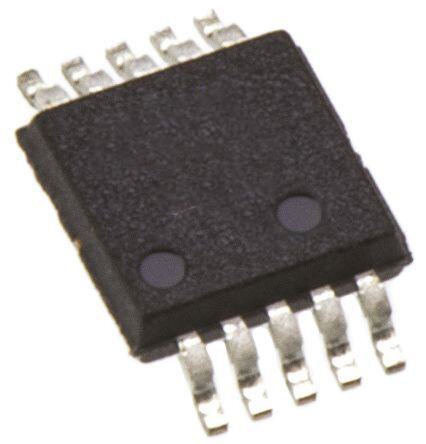
| 供应商器件封装 | 10-MSOP |
| 包装 | 管件 |
| 商标 | Analog Devices |
| 存储器类型 | 易失 |
| 安装类型 | 表面贴装 |
| 安装风格 | SMD/SMT |
| 容差 | 20 % |
| 封装 | Tube |
| 封装/外壳 | 10-TFSOP,10-MSOP(0.118",3.00mm 宽) |
| 封装/箱体 | MSOP-10 |
| 工作温度 | -40°C ~ 125°C |
| 工作电源电压 | 5.5 V |
| 工厂包装数量 | 50 |
| 弧刷存储器 | Volatile |
| 抽头 | 256 |
| 接口 | I²C |
| 数字接口 | I2C |
| 最大工作温度 | + 125 C |
| 最小工作温度 | - 40 C |
| 标准包装 | 50 |
| 每POT分接头 | 256 |
| 温度系数 | 35 PPM / C |
| 电压-电源 | 2.7 V ~ 5.5 V |
| 电源电压-最大 | 5.5 V |
| 电源电压-最小 | 2.7 V |
| 电源电流 | 3.5 uA |
| 电路数 | 2 |
| 电阻 | 10 kOhms |
| 电阻(Ω) | 10k |
| 系列 | AD5243 |
| 配用 | /product-detail/zh/AD5243EVAL/AD5243EVAL-ND/653802 |


- 商务部:美国ITC正式对集成电路等产品启动337调查
- 曝三星4nm工艺存在良率问题 高通将骁龙8 Gen1或转产台积电
- 太阳诱电将投资9.5亿元在常州建新厂生产MLCC 预计2023年完工
- 英特尔发布欧洲新工厂建设计划 深化IDM 2.0 战略
- 台积电先进制程称霸业界 有大客户加持明年业绩稳了
- 达到5530亿美元!SIA预计今年全球半导体销售额将创下新高
- 英特尔拟将自动驾驶子公司Mobileye上市 估值或超500亿美元
- 三星加码芯片和SET,合并消费电子和移动部门,撤换高东真等 CEO
- 三星电子宣布重大人事变动 还合并消费电子和移动部门
- 海关总署:前11个月进口集成电路产品价值2.52万亿元 增长14.8%


PDF Datasheet 数据手册内容提取
Dual, 256-Position, I2C-Compatible Digital Potentiometers Data Sheet AD5243/AD5248 FEATURES FUNCTIONAL BLOCK DIAGRAMS 2-channel, 256-position potentiometers A1 W1 B1 A2 W2 B2 End-to-end resistance: 2.5 kΩ, 10 kΩ, 50 kΩ, and 100 kΩ Compact 10-lead MSOP (3 mm × 4.9 mm) package Fast settling time: t = 5 µs typical on power-up S Full read/write of wiper register VDD Power-on preset to midscale WIPER WIPER REGISTER 1 REGISTER 2 Extra package address decode pins: AD0 and AD1 (AD5248 only) GND Computer software replaces microcontroller in factory programming applications AD5243 Single supply: 2.7 V to 5.5 V LLooww tpeomwpeer:r aItu =re 6 c µoAef mficaixeinmt:u 3m5 ppm/°C SSDCAL PC INTERFACE 04109-0-001 DD Figure 1. AD5243 Wide operating temperature: −40°C to +125°C Evaluation board available W1 B1 W2 B2 APPLICATIONS Systems calibrations VDD Electronics level settings RDAC RDAC Mechanical trimmers replacement in new designs REGISTER 1 REGISTER 2 Permanent factory printed circuit board (PCB) setting GND Transducer adjustment of pressure, temperature, position, chemical, and optical sensors AD0 ADDRESS AD1 DECODE /8 AD5248 RF amplifier biasing G ain control and offset adjustment SSDCAL SERREIGALIS ITNEPRUT 04109-0-002 Figure 2. AD5248 GENERAL DESCRIPTION The AD5243 and AD5248 provide a compact 3 mm × 4.9 mm into the RDAC latch. (The terms digital potentiometer, VR, packaged solution for dual, 256-position adjustment applications. and RDAC are used interchangeably.) The AD5243 performs the same electronic adjustment function Operating from a 2.7 V to 5.5 V power supply and consuming as a 3-terminal mechanical potentiometer, and the AD5248 less than 6 µA allows the AD5243/AD5248 to be used in performs the same adjustment function as a 2-terminal variable portable battery-operated applications. resistor. Available in four end-to-end resistance values (2.5 kΩ, For applications that program the AD5243/AD5248 at the 10 kΩ, 50 kΩ, and 100 kΩ), these low temperature coefficient factory, Analog Devices, Inc., offers device programming devices are ideal for high accuracy and stability-variable software running on Windows® NT/2000/XP operating systems. resistance adjustments. The wiper settings are controllable This software effectively replaces the need for external I2C through the I2C-compatible digital interface. The AD5248 has controllers, which in turn enhances the time to market of extra package address decode pins, AD0 and AD1, allowing systems. An AD5243/AD5248 evaluation kit and software are multiple parts to share the same I2C, 2-wire bus on a PCB. The available. The kit includes a cable and instruction manual. resistance between the wiper and either endpoint of the fixed resistor varies linearly with respect to the digital code transferred Rev. C Document Feedback Information furnished by Analog Devices is believed to be accurate and reliable. However, no responsibility is assumed by Analog Devices for its use, nor for any infringements of patents or other One Technology Way, P.O. Box 9106, Norwood, MA 02062-9106, U.S.A. rights of third parties that may result from its use. Specifications subject to change without notice. No license is granted by implication or otherwise under any patent or patent rights of Analog Devices. Tel: 781.329.4700 ©2004–2016 Analog Devices, Inc. All rights reserved. Trademarks and registered trademarks are the property of their respective owners. Technical Support www.analog.com
AD5243/AD5248 Data Sheet TABLE OF CONTENTS Features .............................................................................................. 1 Test Circuits ..................................................................................... 12 Applications ....................................................................................... 1 Theory of Operation ...................................................................... 13 Functional Block Diagrams ............................................................. 1 Programming the Variable Resistor and Voltage ................... 13 General Description ......................................................................... 1 Programming the Potentiometer Divider ............................... 14 Revision History ............................................................................... 2 ESD Protection ........................................................................... 14 Specifications ..................................................................................... 3 Terminal Voltage Operating Range ......................................... 14 Electrical Characteristics: 2.5 kΩ Version ................................. 3 Power-Up Sequence ................................................................... 14 Electrical Characteristics: 10 kΩ, 50 kΩ, and 100 kΩ Layout and Power Supply Bypassing ....................................... 14 Versions .......................................................................................... 4 Constant Bias to Retain Resistance Setting ............................. 15 Timing Characteristics: All Versions ......................................... 5 I2C Interface .................................................................................... 16 Absolute Maximum Ratings ............................................................ 6 I2C Compatible, 2-Wire Serial Bus .......................................... 16 ESD Caution .................................................................................. 6 I2C Controller Programming .................................................... 18 Pin Configurations and Function Descriptions ........................... 7 Outline Dimensions ....................................................................... 19 Typical Performance Characteristics ............................................. 8 Ordering Guide .......................................................................... 19 REVISION HISTORY 4/16—Rev. B to Rev. C Changes to Applications Section and General Description 4/09—Rev. 0 to Rev. A Section ................................................................................................ 1 Changes to DC Characteristics—Rheostat Mode Parameter and Changed Digital Inputs and Outputs Parameter to Digital to DC Characteristics—Potentiometer Divider Mode Parameter, Inputs Parameter, Table 1 ................................................................ 3 Table 1 .................................................................................................3 Changed Digital Inputs and Outputs Parameter to Digital Moved Figure 3 .................................................................................. 5 Inputs Parameter, Table 2 ................................................................ 4 Updated Outline Dimensions ....................................................... 19 Changes to Ordering Guide .......................................................... 19 Changes to Ordering Guide .......................................................... 19 4/12—Rev. A to Rev. B 1/04—Revision 0: Initial Version Changes to Rheostat Operation Section, Table 7, and Table 8 .............................................................................................. 13 Changes to Voltage Output Operation Section .......................... 14 Deleted Evaluation Board Section and Figure 45, Renumbered Sequentially ..................................................................................... 15 Changes to Table 13 ........................................................................ 17 Updated Outline Dimensions ....................................................... 19 Changes to Ordering Guide .......................................................... 19 Rev. C | Page 2 of 20
Data Sheet AD5243/AD5248 SPECIFICATIONS ELECTRICAL CHARACTERISTICS: 2.5 kΩ VERSION V = 5 V ± 10%, or 3 V ± 10%; V = V ; V = 0 V; −40°C < T < +125°C; unless otherwise noted. DD A DD B A Table 1. Parameter Symbol Conditions Min Typ1 Max Unit DC CHARACTERISTICS—RHEOSTAT MODE Resistor Differential Nonlinearity2 R-DNL R , V = no connect −2 ±0.1 +2 LSB WB A Resistor Integral Nonlinearity2 R-INL R , V = no connect −14 ±2 +14 LSB WB A Nominal Resistor Tolerance3 ∆R T = 25°C −20 +55 % AB A Resistance Temperature Coefficient (∆R /R )/∆T V = V , wiper = no connect 35 ppm/°C AB AB AB DD Wiper Resistance R Code = 0x00, V = 5 V 160 200 Ω WB DD DC CHARACTERISTICS—POTENTIOMETER DIVIDER MODE4 Differential Nonlinearity5 DNL −1.5 ±0.1 +1.5 LSB Integral Nonlinearity5 INL −2 ±0.6 +2 LSB Voltage Divider Temperature Coefficient (∆V /V )/∆T Code = 0x80 15 ppm/°C W W Full-Scale Error V Code = 0xFF −14 −5.5 0 LSB WFSE Zero-Scale Error V Code = 0x00 0 4.5 12 LSB WZSE RESISTOR TERMINALS Voltage Range6 V , V , V GND V V A B W DD Capacitance A, B7 C , C f = 1 MHz, measured to GND, 45 pF A B code = 0x80 Capacitance W7 C f = 1 MHz, measured to GND, 60 pF W code = 0x80 Shutdown Supply Current8 I V = 5.5 V 0.01 1 µA A_SD DD Common-Mode Leakage I V = V = V /2 1 nA CM A B DD DIGITAL INPUTS Input Logic High V V = 5 V 2.4 V IH DD Input Logic Low V V = 5 V 0.8 V IL DD Input Logic High V V = 3 V 2.1 V IH DD Input Logic Low V V = 3 V 0.6 V IL DD Input Current I V = 0 V or 5 V ±1 µA IL IN Input Capacitance7 C 5 pF IL POWER SUPPLIES Power Supply Range V 2.7 5.5 V DD RANGE Supply Current I V = 5 V or V = 0 V 3.5 6 µA DD IH IL Power Dissipation9 P V = 5 V or V = 0 V, V = 5 V 30 µW DISS IH IL DD Power Supply Sensitivity PSS V = 5 V ± 10%, code = midscale ±0.02 ±0.08 %/% DD DYNAMIC CHARACTERISTICS10 Bandwidth, −3 dB BW Code = 0x80 4.8 MHz Total Harmonic Distortion THD V = 1 V rms, V = 0 V, f = 1 kHz 0.1 % W A B V Settling Time t V = 5 V, V = 0 V, ±1 LSB error band 1 µs W S A B Resistor Noise Voltage Density e R = 1.25 kΩ, R = 0 3.2 nV/√Hz N_WB WB S 1 Typical specifications represent average readings at 25°C and VDD = 5 V. 2 Resistor position nonlinearity error, R-INL, is the deviation from an ideal value measured between the maximum resistance and the minimum resistance wiper positions. R-DNL measures the relative step change from the ideal between successive tap positions. Parts are guaranteed monotonic. 3 VA = VDD, VB = 0 V, wiper (VW) = no connect. 4 Specifications apply to all VRs. 5 INL and DNL are measured at VW with the RDAC configured as a potentiometer divider similar to a voltage output digital-to-analog converter (DAC). VA = VDD and VB = 0 V. DNL specification limits of ±1 LSB maximum are guaranteed monotonic operating conditions. 6 Resistor Terminal A, Resistor Terminal B, and Resistor Terminal W have no limitations on polarity with respect to each other. 7 Guaranteed by design, but not subject to production test. 8 Measured at the A terminal. The A terminal is open circuited in shutdown mode. 9 PDISS is calculated from (IDD × VDD). CMOS logic level inputs result in minimum power dissipation. 10 All dynamic characteristics use VDD = 5 V. Rev. C | Page 3 of 20
AD5243/AD5248 Data Sheet ELECTRICAL CHARACTERISTICS: 10 kΩ, 50 kΩ, AND 100 kΩ VERSIONS V = 5 V ± 10%, or 3 V ± 10%; V = V ; V = 0 V; −40°C < T < 125°C; unless otherwise noted. DD A DD B A Table 2. Parameter Symbol Conditions Min Typ1 Max Unit DC CHARACTERISTICS—RHEOSTAT MODE Resistor Differential Nonlinearity2 R-DNL R , V = no connect −1 ±0.1 +1 LSB WB A Resistor Integral Nonlinearity2 R-INL R , V = no connect −2.5 ±0.25 +2.5 LSB WB A Nominal Resistor Tolerance3 ∆R T = 25°C −20 +20 % AB A Resistance Temperature Coefficient (∆R /R )/∆T V = V , wiper = no connect 35 ppm/°C AB AB AB DD Wiper Resistance R Code = 0x00, V = 5 V 160 200 Ω WB DD DC CHARACTERISTICS—POTENTIOMETER DIVIDER MODE4 Differential Nonlinearity5 DNL −1 ±0.1 +1 LSB Integral Nonlinearity5 INL −1 ±0.3 +1 LSB Voltage Divider Temperature Coefficient (∆V /V )/∆T Code = 0x80 15 ppm/°C W W Full-Scale Error V Code = 0xFF −2.5 −1 0 LSB WFSE Zero-Scale Error V Code = 0x00 0 1 2.5 LSB WZSE RESISTOR TERMINALS Voltage Range6 V , V, V GND V V A B W DD Capacitance A, B7 C , C f = 1 MHz, measured to GND, 45 pF A B code = 0x80 Capacitance W7 C f = 1 MHz, measured to GND, 60 pF W code = 0x80 Shutdown Supply Current8 I V = 5.5 V 0.01 1 µA A_SD DD Common-Mode Leakage I V = V = V /2 1 nA CM A B DD DIGITAL INPUTS Input Logic High V V = 5 V 2.4 V IH DD Input Logic Low V V = 5 V 0.8 V IL DD Input Logic High V V = 3 V 2.1 V IH DD Input Logic Low V V = 3 V 0.6 V IL DD Input Current I V = 0 V or 5 V ±1 µA IL IN Input Capacitance C 5 pF IL POWER SUPPLIES Power Supply Range V 2.7 5.5 V DD RANGE Supply Current I V = 5 V or V = 0 V 3.5 6 µA DD IH IL Power Dissipation P V = 5 V or V = 0 V, V = 5 V 30 µW DISS IH IL DD Power Supply Sensitivity PSS V = 5 V ± 10%, code = midscale ±0.02 ±0.08 %/% DD DYNAMIC CHARACTERISTICS Bandwidth, −3 dB BW R = 10 kΩ/50 kΩ/100 kΩ, code = 0x80 600/100/40 kHz AB Total Harmonic Distortion THD V = 1 V rms, V = 0 V, f = 1 kHz, 0.1 % W A B R = 10 kΩ AB V Settling Time t V = 5 V, V = 0 V, ±1 LSB error band 2 µs W S A B Resistor Noise Voltage Density e R = 5 kΩ, R = 0 9 nV/√Hz N_WB WB S 1 Typical specifications represent average readings at 25°C and VDD = 5 V. 2 Resistor position nonlinearity error, R-INL, is the deviation from an ideal value measured between the maximum resistance and the minimum resistance wiper positions. R-DNL measures the relative step change from the ideal between successive tap positions. Parts are guaranteed monotonic. 3 VA = VDD, VB = 0 V, wiper (VW) = no connect. 4 Specifications apply to all VRs. 5 INL and DNL are measured at VW with the RDAC configured as a potentiometer divider similar to a voltage output DAC. VA = VDD and VB = 0 V. DNL specification limits of ±1 LSB maximum are guaranteed monotonic operating conditions. 6 Resistor Terminal A, Resistor Terminal B, and Resistor Terminal W have no limitations on polarity with respect to each other. 7 Guaranteed by design, but not subject to production test. 8 Measured at the A terminal. The A terminal is open circuited in shutdown mode. Rev. C | Page 4 of 20
Data Sheet AD5243/AD5248 TIMING CHARACTERISTICS: ALL VERSIONS V = 5 V ± 10%, or 3 V ± 10%; V = V ; V = 0 V; −40°C < T < +125°C; unless otherwise noted. DD A DD B A Table 3. Parameter Symbol Conditions Min Typ Max Unit I2C INTERFACE TIMING CHARACTERISTICS1 SCL Clock Frequency f 0 400 kHz SCL Bus-Free Time Between Stop and Start, t t 1.3 μs BUF 1 Hold Time (Repeated Start), t t After this period, the first clock pulse is 0.6 μs HD;STA 2 generated. Low Period of SCL Clock, t t 1.3 μs LOW 3 High Period of SCL Clock, t t 0.6 μs HIGH 4 Setup Time for Repeated Start Condition, t t 0.6 μs SU;STA 5 Data Hold Time, tHD;DAT2 t6 0.9 μs Data Setup Time, t t 100 ns SU;DAT 7 Fall Time of Both SDA and SCL Signals, t t 300 ns F 8 Rise Time of Both SDA and SCL Signals, t t 300 ns R 9 Setup Time for Stop Condition, t t 0.6 μs SU;STO 10 1 See the timing diagrams for the locations of measured values (that is, see Figure 3 and Figure 45 to Figure 48). 2 The maximum tHD:DAT must be met only if the device does not stretch the low period (tLOW) of the SCL signal. t8 t6 t9 t2 SCL t2 t3 t4 t7 t5 t10 t8 t9 SDA P t1 S S P 04109-0-021 Figure 3. I2C Interface Detailed Timing Diagram Rev. C | Page 5 of 20
AD5243/AD5248 Data Sheet ABSOLUTE MAXIMUM RATINGS T = 25°C, unless otherwise noted. A Stresses at or above those listed under Absolute Maximum Ratings may cause permanent damage to the product. This is a Table 4. stress rating only; functional operation of the product at these Parameter Rating or any other conditions above those indicated in the operational V to GND −0.3 V to +7 V DD section of this specification is not implied. Operation beyond V , V , V to GND V A B W DD the maximum operating conditions for extended periods may Terminal Current, Ax to Bx, Ax to Wx, Bx to Wx1 affect product reliability. Pulsed ±20 mA Continuous ±5 mA ESD CAUTION Digital Inputs and Output Voltage to GND 0 V to 7 V Operating Temperature Range −40°C to +125°C Maximum Junction Temperature (T ) 150°C JMAX Storage Temperature −65°C to +150°C Lead Temperature (Soldering, 10 sec) 300°C Thermal Resistance, θJA for 10-Lead MSOP2 230°C/W 1The maximum terminal current is bound by the maximum current handling of the switches, the maximum power dissipation of the package, and the maximum applied voltage across any two of the A, B, and W terminals at a given resistance. 2The package power dissipation is (TJMAX − TA)/θJA. Rev. C | Page 6 of 20
Data Sheet AD5243/AD5248 PIN CONFIGURATIONS AND FUNCTION DESCRIPTIONS B1 1 10 W1 B1 1 10 W1 A1 2 9 B2 AD0 2 9 B2 W2 3 AD5243 8 A2 W2 3 AD5248 8 AD1 GVNDDD 54 TOP VIEW 67 SSDCAL 04109-0-027 GVNDDD 45 TOP VIEW 76 SSDCAL 04109-0-028 Figure 4. AD5243 Pin Configuration Figure 5. AD5248 Pin Configuration Table 5. AD5243 Pin Function Descriptions Table 6. AD5248 Pin Function Descriptions Pin Pin No. Mnemonic Description No. Mnemonic Description 1 B1 B1 Terminal. 1 B1 B1 Terminal. 2 A1 A1 Terminal. 2 AD0 Programmable Address Bit 0 for Multiple 3 W2 W2 Terminal. Package Decoding. 4 GND Digital Ground. 3 W2 W2 Terminal. 5 V Positive Power Supply. 4 GND Digital Ground. DD 6 SCL Serial Clock Input. Positive-edge 5 VDD Positive Power Supply. triggered. 6 SCL Serial Clock Input. Positive-edge 7 SDA Serial Data Input/Output. triggered. 8 A2 A2 Terminal. 7 SDA Serial Data Input/Output. 9 B2 B2 Terminal. 8 AD1 Programmable Address Bit 1 for Multiple Package Decoding. 10 W1 W1 Terminal. 9 B2 B2 Terminal. 10 W1 W1 Terminal. Rev. C | Page 7 of 20
AD5243/AD5248 Data Sheet TYPICAL PERFORMANCE CHARACTERISTICS 2.0 0.5 TA = 25°C RAB = 10kΩ 1.5 RAB = 10kΩ 0.4 B) S 0.3 SB) 1.0 VDD = 2.7V L (L L N 0.2 NL ( 0.5 E D E I OD 0.1 VDD = 2.7V; TA =–40°C, +25°C, +85°C, +125°C D M MO 0 R 0 TAT –0.5 VDD = 5.5V METE –0.1 RHEOS –1.0 OTENTIO ––00..32 P –1.5 –0.4 –2.00 32 64 9C6ODE (1D2E8CIMA1L6)0 192 224 256 04109-0-030 –0.50 32 64 9C6ODE (1D2E8CIMA1L6)0 192 224 256 04109-0-033 Figure 6. R-INL vs. Code vs. Supply Voltages Figure 9. DNL vs. Code vs. Temperature 0.5 1.0 TA = 25°C TA = 25°C 0.4 RAB = 10kΩ 0.8 RAB = 10kΩ B) B) 0.3 LS 0.6 ODE DNL (LS 00..012 VDD = 2.7V R MODE INL ( 00..024 VDD = 5.5V M E AT –0.1 MET –0.2 VDD = 2.7V EOST –0.2 NTIO –0.4 H E R –0.3 VDD = 5.5V OT –0.6 P –0.4 –0.8 –0.50 32 64 9C6ODE (1D2E8CIMA1L6)0 192 224 256 04109-0-031 –1.00 32 64 9C6ODE (1D2E8CIMA1L6)0 192 224 256 04109-0-034 Figure 7. R-DNL vs. Code vs. Supply Voltages Figure 10. INL vs. Code vs. Supply Voltages 0.5 0.5 RAB = 10kΩ TA = 25°C 0.4 0.4 RAB = 10kΩ E INL (LSB) 00..23 VTAD D= =– 450.5°VC, +25°C, +85°C, +125°C E DNL (LSB) 00..23 MOD 0.1 MOD 0.1 VDD = 2.7V R 0 R 0 METE –0.1 METE –0.1 OTENTIO ––00..32 VTAD D= =– 420.7°VC, +25°C, +85°C, +125°C OTENTIO ––00..32 VDD = 5.5V P P –0.4 –0.4 –0.50 32 64 9C6ODE (1D2E8CIMA1L6)0 192 224 256 04109-0-032 –0.50 32 64 9C6ODE (1D2E8CIMA1L6)0 192 224 256 04109-0-035 Figure 8. INL vs. Code vs. Temperature Figure 11. DNL vs. Code vs. Supply Voltages Rev. C | Page 8 of 20
Data Sheet AD5243/AD5248 2.0 4.50 RAB = 10kΩ RAB = 10kΩ 1.5 VDD = 2.7V TA =–40°C, +25°C, +85°C, +125°C B) 3.75 NL (LSB) 01..50 ROR (LS 3.00 E I ER MOD 0 ALE 2.25 VDD = 2.7V, VA = 2.7V OSTAT –0.5 VTAD D= =– 450.5°VC, +25°C, +85°C, +125°C ERO-SC 1.50 E Z RH –1.0 E, VDD = 5.5V, VA = 5.0V S Z 0.75 –1.5 –2.00 32 64 9C6ODE (1D2E8CIMA1L6)0 192 224 256 04109-0-036 0–40 –25 –10 5 T2E0MPE3R5ATU50RE (°6C5) 80 95 110 125 04109-0-039 Figure 12. R-INL vs. Code vs. Temperature Figure 15. Zero-Scale Error vs. Temperature 0.5 10 RAB = 10kΩ 0.4 E DNL (LSB) 000...123 VDD = 2.7V, 5.5V; TA =–40°C, +25°C, +85°C, +125°C µRRENT (A) VDD = 5V D U O 0 C 1 M Y STAT –0.1 UPPL VDD = 3V RHEO ––00..32 I, SDD –0.4 –0.50 32 64 9C6ODE (1D2E8CIMA1L6)0 192 224 256 04109-0-037 0.1–40 –7 TE2M6PERATURE5 9(°C) 92 125 04109-0-040 Figure 13. R-DNL vs. Code vs. Temperature Figure 16. Supply Current vs. Temperature 2.0 120 RAB = 10kΩ RAB = 10kΩ 1.5 C) 100 B) m/° ULL-SCALE ERROR (LS –001...5050 VDD = 5.5V, VA = 5.0V AT MODE TEMPCO (pp 468000 VTAD D= =– 420.7°VC TOVTAD + D=8 5=–° 45C0.,5°–VC4 T0°OC + T8O5° +C1,2–54°0C°C TO +125°C E, F –1.0 VDD = 2.7V, VA = 2.7V OST 20 S E F H –1.5 R 0 –2.0–40 –25 –10 5 T2E0MPE3R5ATU50RE (°6C5) 80 95 110 125 04109-0-038 –200 32 64 9C6ODE (1D2E8CIMA1L6)0 192 224 256 04109-0-041 Figure 14. Full-Scale Error vs. Temperature Figure 17. Rheostat Mode Tempco ΔRWB/ΔT vs. Code Rev. C | Page 9 of 20
AD5243/AD5248 Data Sheet 50 0 m/°C) 40 RAB = 10kΩ –6 0x80 pp –12 0x40 ODE TEMPCO ( 123000 VTAD D= =– 420.7°VC TO +85°C,–40°C TO +125°C N (dB) –––213048 000xxx210008 ER M 0 GAI –36 0x04 ET 0x02 M –42 TIO –10 VDD = 5.5V 0x01 EN TA =–40°C TO +85°C,–40°C TO +125°C –48 POT –20 –54 –300 32 64 9C6ODE (1D2E8CIMA1L6)0 192 224 256 04109-0-042 –601k 10kFREQUENCY (Hz1)00k 1M 04109-0-045 Figure 18. Potentiometer Mode Tempco ΔVWB/ΔT vs. Code Figure 21. Gain vs. Frequency vs. Code, RAB = 50 kΩ 0 0 0x80 0x80 –6 –6 0x40 0x40 –12 –12 0x20 0x20 –18 –18 0x10 0x10 B) –24 0x08 B) –24 N (d –30 0x04 N (d –30 0x08 AI AI G –36 G –36 0x04 0x02 0x01 0x02 –42 –42 0x01 –48 –48 –54 –54 –6010k 100kFREQUENCY (Hz)1M 10M 04109-0-043 –601k 10kFREQUENCY (Hz1)00k 1M 04109-0-046 Figure 19. Gain vs. Frequency vs. Code, RAB = 2.5 kΩ Figure 22. Gain vs. Frequency vs. Code, RAB = 100 kΩ 0 0 0x80 –6 –6 –12 0x40 –12 100kΩ –18 0x20 –18 60kHz 50kΩ B) –24 0x10 B) –24 120kHz 10kΩ AIN (d –30 00xx0084 AIN (d –30 570kHz2.5kΩ G –36 0x02 G –36 2.2MHz 0x01 –42 –42 –48 –48 –54 –54 –601k 10kFREQUENCY (Hz1)00k 1M 04109-0-044 –601k 10k FREQU1E00NkCY (Hz) 1M 10M 04109-0-047 Figure 20. Gain vs. Frequency vs. Code, RAB = 10 kΩ Figure 23. –3 dB Bandwidth at Code = 0x80 Rev. C | Page 10 of 20
Data Sheet AD5243/AD5248 10 TA = 25°C A) m T ( 1 N RE VDD = 5.5V R CU VW2 Y L P P SU 0.1 , D ID VDD = 2.7V VW1 0.010 0.5 1.0 D1I.G5ITA2L. 0INPU2T.5 VOL3T.0AGE3 (.V5) 4.0 4.5 5.0 04109-0-052 04109-0-051 Figure 24. Supply Current vs. Digital Input Voltage Figure 27. Analog Crosstalk VW VW SCL 04109-0-048 04109-0-053 Figure 25. Digital Feedthrough Figure 28. Midscale Glitch, Code 0x80 to Code 0x7F VW2 VW VW1 SCL 04109-0-049 04109-0-050 Figure 26. Digital Crosstalk Figure 29. Large-Signal Settling Time Rev. C | Page 11 of 20
AD5243/AD5248 Data Sheet TEST CIRCUITS Figure 30 through Figure 36 illustrate the test circuits that define the test conditions used in the product specification tables (see Table 1 and Table 2). DUT +15V DUT V+ = VDD A W A 1LSB = V+/2N VIN W B AD8610 VOUT V+ OFFSET B VMS 04109-0-003 GND 2.5V –15V 04109-0-009 Figure 30. Test Circuit for Potentiometer Divider Nonlinearity Error Figure 34. Test Circuit for Gain vs. Frequency (INL, DNL) 0.1V NO CONNECT DUT RSW= ISW DUT CODE = 0x00 A W IW W B ISW 0.1V B VMS 04109-0-004 VSS TO VDD 04109-0-010 Figure 31. Test Circuit for Resistor Position Nonlinearity Error Figure 35. Test Circuit for Incremental On Resistance (Rheostat Operation: R-INL, R-DNL) NC DUT DUT A W VW IW = VDD/RNOMINAL VDD A W ICM VMS2 B VMS1 RW = [VMS1– VMS2]/IW 04109-0-005 GND NCB NC = NO CONNECT VCM 04109-0-011 Figure 32. Test Circuit for Wiper Resistance Figure 36. Test Circuit for Common-Mode Leakage Current VA V+ = VDD± 10% ( ∆ V M S ) V+ ∆VDD ADWUT PPSSRS R(% (d/%B)) == ∆∆20VV MDLDSO%%G ∆VDD B VMS 04109-0-006 Figure 33. Test Circuit for Power Supply Sensitivity (PSS, PSSR) Rev. C | Page 12 of 20
Data Sheet AD5243/AD5248 THEORY OF OPERATION The general equation determining the digitally programmed The AD5243/AD5248 are 256-position, digitally controlled output resistance between W and B is variable resistor (VR) devices. D An internal power-on preset places the wiper at midscale R (D) R 2R (1) during power-on, which simplifies the fault condition recovery WB 256 AB W at power-up. where: PROGRAMMING THE VARIABLE RESISTOR AND D is the decimal equivalent of the binary code loaded in the 8-bit RDAC register. VOLTAGE R is the end-to-end resistance. AB Rheostat Operation R is the wiper resistance contributed by the on resistance of W The nominal resistance of the RDAC between Terminal A and the internal switch. Terminal B is available in 2.5 kΩ, 10 kΩ, 50 kΩ, and 100 kΩ. In summary, if R is 10 kΩ and the A terminal is open circuited, The nominal resistance (R ) of the VR has 256 contact points AB AB the following output resistance, R , is set for the indicated accessed by the wiper terminal and the B terminal contact. The WB RDAC latch codes. 8-bit data in the RDAC latch is decoded to select one of the 256 possible settings. Table 7. Codes and Corresponding R Resistance WB D (Dec) R (Ω) Output State WB A A A 255 10,281 Full scale (R − 1 LSB + 2 × R ) AB W W W W 128 5380 Midscale B B B 04109-0-012 10 335290 1Z eLrSoB s +ca 2le × ( wRWip er contact resistance) Figure 37. Rheostat Mode Configuration Assuming that a 10 kΩ part is used, the first connection of the Note that in the zero-scale condition, a finite wiper resistance of wiper starts at the B terminal for Data 0x00. Because there is 320 Ω is present. Care should be taken to limit the current flow a 160 Ω wiper contact resistance, such a connection yields a between W and B in this state to a maximum pulse current of no minimum of 320 Ω (2 × 160 Ω) resistance between Terminal W more than 20 mA. Otherwise, degradation or possible destruction and Terminal B. The second connection is the first tap point, of the internal switch contact may occur. which corresponds to 359 Ω (R = R /256 + 2 × R = 39 Ω + WB AB W Similar to the mechanical potentiometer, the resistance of the 2 × 160 Ω) for Data 0x01. The third connection is the next tap RDAC between Wiper W and Terminal A also produces a point, representing 398 Ω (2 × 39 Ω + 2 × 160 Ω) for Data 0x02, digitally controlled complementary resistance, R . When these and so on. Each LSB data value increase moves the wiper up the WA terminals are used, the B terminal can be opened. Setting the resistor ladder until the last tap point is reached at 10,281 Ω resistance value for R starts at a maximum value of resistance (R + 2 × R ). WA AB W and decreases as the data loaded in the latch increases in value. A The general equation for this operation is RS 256D R (D) R 2R (2) WA 256 AB W DD76 RS When RAB is 10 kΩ and the B terminal is open circuited, the D5 DD43 RS output resistance, RWA, is set according to the RDAC latch D2 codes, as listed in Table 8. D1 D0 W Table 8. Codes and Corresponding R Resistance WA D (Dec) R (Ω) Output State WA 255 359 Full scale 128 5320 Midscale RDAC RS 1 10,280 1 LSB + 2 × R W LATCH AND B 0 10,320 Zero scale DECODER 04109-0-013 Typical device-to-device matching is process-lot dependent and Figure 38. AD5243 Equivalent RDAC Circuit may vary by up to ±30%. Because the resistance element is pro- cessed in thin-film technology, the change in R with temperature AB has a very low temperature coefficient of 35 ppm/°C. Rev. C | Page 13 of 20
AD5243/AD5248 Data Sheet PROGRAMMING THE POTENTIOMETER DIVIDER TERMINAL VOLTAGE OPERATING RANGE Voltage Output Operation The AD5243/AD5248 V and GND power supply defines the DD The digital potentiometer easily generates a voltage divider at boundary conditions for proper 3-terminal digital potentiometer wiper to B and wiper to A, proportional to the input voltage at operation. Supply signals present on the A, B, and W terminals A to B. Unlike the polarity of VDD to GND, which must be that exceed VDD or GND are clamped by the internal forward- positive, voltage across A to B, W to A, and W to B can be at biased diodes (see Figure 42). either polarity. VDD VI A A W W VO B B 04109-0-014 GND 04109-0-017 Figure 39. Potentiometer Mode Configuration Figure 42. Maximum Terminal Voltages Set by VDD and GND If ignoring the effect of the wiper resistance for approximation, POWER-UP SEQUENCE connecting the A terminal to 5 V and the B terminal to ground Because the ESD protection diodes limit the voltage compliance produces an output voltage at the wiper to B, starting at 0 V up at the A, B, and W terminals (see Figure 42), it is important to to 1 LSB less than 5 V. Each LSB of voltage is equal to the voltage power V /GND before applying voltage to the A, B, and W applied across Terminal A and Terminal B divided by the DD terminals; otherwise, the diode is forward-biased such that V 256 positions of the potentiometer divider. The general equation DD is powered unintentionally and may affect the rest of the user’s defining the output voltage at V with respect to ground for any W circuit. The ideal power-up sequence is in the following order: valid input voltage applied to Terminal A and Terminal B is GND, V , digital inputs, and then V , V , and V . The relative DD A B W D 256−D V (D)= V + V (3) order of powering VA, VB, VW, and the digital inputs is not W 256 A 256 B important, as long as they are powered after V /GND. DD Operation of the digital potentiometer in the divider mode LAYOUT AND POWER SUPPLY BYPASSING results in more accurate operation over temperature. Unlike in It is a good practice to employ compact, minimum lead length the rheostat mode, the output voltage is dependent mainly on layout design. The leads to the inputs should be as direct as the ratio of the internal resistors, R and R , not on the WA WB possible with a minimum conductor length. Ground paths absolute values. Therefore, the temperature drift reduces to should have low resistance and low inductance. 15 ppm/°C. ESD PROTECTION Similarly, it is also good practice to bypass the power supplies with quality capacitors for optimum stability. Supply leads to the device All digital inputs are protected with a series of input resistors should be bypassed with disc or chip ceramic capacitors of 0.01 µF and parallel Zener ESD structures, as shown in Figure 40 and to 0.1 µF. Low ESR 1 µF to 10 µF tantalum or electrolytic capacitors Figure 41. This applies to the SDA, SCL, AD0, and AD1 digital should also be applied at the supplies to minimize any transient input pins (AD5248 only). disturbance and low frequency ripple (see Figure 43). In addition, 340Ω note that the digital ground should be joined remotely to the LOGIC GND 04109-0-015 analog ground at one point to minimize the ground bounce. Figure 40. ESD Protection of Digital Pins VDD VDD + C3 C1 A, B, W 10µF 0.1µF AD5243 GND 04109-0-016 GND Figure 41. ESD Protection of Resistor Terminals 04109-0-018 Figure 43. Power Supply Bypassing Rev. C | Page 14 of 20
Data Sheet AD5243/AD5248 CONSTANT BIAS TO RETAIN RESISTANCE SETTING This demonstrates that constantly biasing the potentiometer can be a practical approach. Most portable devices do not For users who desire nonvolatility but cannot justify the addi- require the removal of batteries for the purpose of charging. tional cost of an EEMEM, the AD5243/AD5248 can be considered Although the resistance setting of the AD5243/AD5248 is lost low cost alternatives by maintaining a constant bias to retain the when the battery needs replacement, such events occur rather wiper setting. The AD5243/AD5248 are designed specifically for infrequently such that this inconvenience is justified by the low power applications, allowing low power consumption even lower cost and smaller size offered by the AD5243/AD5248. If in battery-operated systems. The graph in Figure 44 demonstrates total power is lost, the user should be provided with a means to the power consumption from a 3.4 V, 450 mAhr Li-Ion cell phone adjust the setting accordingly. battery connected to the AD5243/AD5248. The measurement over time shows that the device draws approximately 1.3 µA and consumes negligible power. Over a course of 30 days, the battery is depleted by less than 2%, the majority of which is due to the intrinsic leakage current of the battery itself. 110 108 TA= 25°C 106 %) D ( 104 E T LE 102 P E D 100 E F LI 98 Y R E 96 T T BA 94 92 900 5 10 DA1Y5S 20 25 30 04109-0-019 Figure 44. Battery Operating Life Depletion Rev. C | Page 15 of 20
AD5243/AD5248 Data Sheet I2C INTERFACE I2C COMPATIBLE, 2-WIRE SERIAL BUS SDA line must occur during the low period of SCL and remain stable during the high period of SCL (see Figure 45 The 2-wire, I2C-compatible serial bus protocol operates as follows: and Figure 46). 1. The master initiates data transfer by establishing a start 3. In the read mode, the data byte follows immediately after the condition, which is when a high-to-low transition on the acknowledgment of the slave address byte. Data is transmitted SDA line occurs while SCL is high (see Figure 45). The over the serial bus in sequences of nine clock pulses (a slight following byte is the slave address byte, which consists of difference with the write mode, where there are eight data bits the slave address followed by an R/W bit (this bit deter- followed by an acknowledge bit). Similarly, the transitions mines whether data is read from or written to the slave on the SDA line must occur during the low period of SCL and device). The AD5243 has a fixed slave address byte, remain stable during the high period of SCL (see Figure 47 whereas the AD5248 has two configurable address bits, and Figure 48). AD0 and AD1 (see Figure 10). Note that the channel of interest is the one that is previously The slave whose address corresponds to the transmitted selected in write mode. If users need to read the RDAC address responds by pulling the SDA line low during the values of both channels, they need to program the first ninth clock pulse (this is called the acknowledge bit). At channel in write mode and then change to read mode to this stage, all other devices on the bus remain idle while the read the first channel value. After that, the user must return selected device waits for data to be written to or read from the device to write mode with the second channel selected its serial register. If the R/W bit is high, the master reads and read the second channel value in read mode. It is not from the slave device. On the other hand, if the R/W bit is necessary for users to issue the Frame 3 data byte in write low, the master writes to the slave device. mode for subsequent readback operation. Users should refer 2. In the write mode, the second byte is the instruction byte. to Figure 47 and Figure 48 for the programming format. The first bit (MSB) of the instruction byte is the RDAC 4. After all data bits have been read or written, a stop condition subaddress select bit. A logic low selects Channel 1 and a is established by the master. A stop condition is defined as logic high selects Channel 2. a low-to-high transition on the SDA line while SCL is high. The second MSB, SD, is a shutdown bit. A logic high causes In write mode, the master pulls the SDA line high during an open circuit at Terminal A while shorting the wiper to the 10th clock pulse to establish a stop condition (see Figure Terminal B. This operation yields almost 0 Ω in rheostat 45 and Figure 46). In read mode, the master issues a no mode or 0 V in potentiometer mode. It is important to acknowledge for the ninth clock pulse (that is, the SDA line note that the shutdown operation does not disturb the remains high). The master then brings the SDA line low contents of the register. When the AD5243 or AD5248 is before the 10th clock pulse, which goes high to establish a brought out of shutdown, the previous setting is applied to stop condition (see Figure 47 and Figure 48). the RDAC. In addition, during shutdown, new settings can A repeated write function provides the user with the flexibility be programmed. When the part is returned from shutdown, of updating the RDAC output multiple times after addressing the corresponding VR setting is applied to the RDAC. and instructing the part only once. For example, after the The remainder of the bits in the instruction byte are don’t RDAC has acknowledged its slave address and instruction care bits (see Figure 10). bytes in write mode, the RDAC output updates on each successive byte. If different instructions are needed, however, After acknowledging the instruction byte, the last byte in the write/read mode must restart with a new slave address, write mode is the data byte. Data is transmitted over the instruction, and data byte. Similarly, a repeated read function serial bus in sequences of nine clock pulses (eight data bits of the RDAC is also allowed. followed by an acknowledge bit). The transitions on the Rev. C | Page 16 of 20
Data Sheet AD5243/AD5248 Write Mode Table 9. AD5243 Write Mode S 0 1 0 1 1 1 1 W A A0 SD X X X X X X A D7 D6 D5 D4 D3 D2 D1 D0 A P Slave address byte Instruction byte Data byte Table 10. AD5248 Write Mode S 0 1 0 1 1 AD1 AD0 W A A0 SD X X X X X X A D7 D6 D5 D4 D3 D2 D1 D0 A P Slave address byte Instruction byte Data byte Read Mode Table 11. AD5243 Read Mode S 0 1 0 1 1 1 1 R A D7 D6 D5 D4 D3 D2 D1 D0 A P Slave address byte Data byte Table 12. AD5248 Read Mode S 0 1 0 1 1 AD1 AD0 R A D7 D6 D5 D4 D3 D2 D1 D0 A P Slave address byte Data byte Table 13. SDA Bits Descriptions Bit Description S Start condition. P Stop condition. A Acknowledge. AD0, AD1 Package pin-programmable address bits. X Don’t care. W Write. R Read. A0 RDAC subaddress select bit. SD Shutdown connects wiper to B terminal and open circuits the A terminal. It does not change the contents of the wiper register. D7, D6, D5, D4, D3, D2, D1, D0 Data bits. Rev. C | Page 17 of 20
AD5243/AD5248 Data Sheet I2C CONTROLLER PROGRAMMING Write Bit Patterns 1 9 1 9 1 9 SCL SDA 0 1 0 1 1 1 1 R/WAACDK52 B43YA0 SD X X X X X XAACDK52 B43YD7 D6 D5 D4 D3 D2 D1 D0AADCK52 B43Y 04109-0-022 START BY FRAME 1 FRAME 2 FRAME 3 STOP BY MASTER SLAVE ADDRESS BYTE INSTRUCTION BYTE DATA BYTE MASTER Figure 45. Writing to the RDAC Register—AD5243 1 9 1 9 1 9 SCL SDA 0 1 0 1 1 AD1AD0 R/WAACDK52 B48YA0 SD X X X X X XAACDK52 B48YD7 D6 D5 D4 D3 D2 D1 D0AACDK52 B48Y 04109-0-023 START BY FRAME 1 FRAME 2 FRAME 3 STOP BY MASTER SLAVE ADDRESS BYTE INSTRUCTION BYTE DATA BYTE MASTER Figure 46. Writing to the RDAC Register—AD5248 Read Bit Patterns 1 9 1 9 SCL SDA 0 1 0 1 1 1 1 R/W D7 D6 D5 D4 D3 D2 D1 D0 ACK BY NO ACK SMTAASRTTE RBY SLAVE FARDADMREE S1S BYTE AD5243 RDAFCR RAEMGEI S2TER BY MSMATASOTSPET REBRY 04109-0-024 Figure 47. Reading Data from a Previously Selected RDAC Register in Write Mode—AD5243 1 9 1 9 SCL SDA 0 1 0 1 1 AD1AD0R/W D7 D6 D5 D4 D3 D2 D1 D0 ACK BY NO ACK SMTAASRTTE RBY SLAVE FARDADMREE S1S BYTE AD5248 RDAFCR RAEMGEI S2TER BY MASMSTTAOESPRT EBRY 04109-0-025 Figure 48. Reading Data from a Previously Selected RDAC Register in Write Mode—AD5248 Multiple Devices on One Bus (Applies Only to AD5248) 5V Figure 49 shows four AD5248 devices on the same serial bus. RP RP Each has a different slave address because the states of their SDA MASTER AD0 and AD1 pins are different. This allows each device on the SCL bus to be written to or read from independently. The master 5V 5V 5V device output bus line drivers are open-drain pull-downs in a fully I2C-compatible interface. SDA SCL SDA SCL SDA SCL SDA SCL AD1 AD1 AD1 AD1 AADD05248 AADD05248 AADD05248 AADD05248 04109-0-026 Figure 49. Multiple AD5248 Devices on One I2C Bus Rev. C | Page 18 of 20
Data Sheet AD5243/AD5248 OUTLINE DIMENSIONS 3.10 3.00 2.90 10 6 5.15 3.10 4.90 3.00 4.65 2.90 1 5 PIN1 IDENTIFIER 0.50BSC 0.95 15°MAX 0.85 1.10MAX 0.75 0.70 0.15 0.30 6° 0.23 0.55 CO0P.0L5ANARITY 0.15 0° 0.13 0.40 0.10 COMPLIANTTOJEDECSTANDARDSMO-187-BA 091709-A Figure 50. 10-Lead Mini Small Outline Package [MSOP] (RM-10) Dimensions shown in millimeters ORDERING GUIDE Model1, 2 R Temperature Package Description Package Option Branding AB AD5243BRM2.5 2.5 kΩ −40°C to +125°C 10-Lead MSOP RM-10 D0L AD5243BRM10 10 kΩ −40°C to +125°C 10-Lead MSOP RM-10 D0M AD5243BRM100 100 kΩ −40°C to +125°C 10-Lead MSOP RM-10 D0P AD5243BRMZ2.5 2.5 kΩ −40°C to +125°C 10-Lead MSOP RM-10 D9X AD5243BRMZ2.5-RL7 2.5 kΩ −40°C to +125°C 10-Lead MSOP RM-10 D9X AD5243BRMZ10 10 kΩ −40°C to +125°C 10-Lead MSOP RM-10 D0M AD5243BRMZ10-RL7 10 kΩ −40°C to +125°C 10-Lead MSOP RM-10 D0M AD5243BRMZ50 50 kΩ −40°C to +125°C 10-Lead MSOP RM-10 D0N AD5243BRMZ50-RL7 50 kΩ −40°C to +125°C 10-Lead MSOP RM-10 D0N AD5243BRMZ100 100 kΩ −40°C to +125°C 10-Lead MSOP RM-10 D0P AD5243BRMZ100-RL7 100 kΩ −40°C to +125°C 10-Lead MSOP RM-10 D0P EVAL-AD5243SDZ Evaluation Board AD5248BRM100 100 kΩ −40°C to +125°C 10-Lead MSOP RM-10 D1J AD5248BRMZ2.5 2.5 kΩ −40°C to +125°C 10-Lead MSOP RM-10 D1F AD5248BRMZ2.5-RL7 2.5 kΩ −40°C to +125°C 10-Lead MSOP RM-10 D1F AD5248BRMZ10 10 kΩ −40°C to +125°C 10-Lead MSOP RM-10 D8Z AD5248BRMZ10-RL7 10 kΩ −40°C to +125°C 10-Lead MSOP RM-10 D8Z AD5248BRMZ50 50 kΩ −40°C to +125°C 10-Lead MSOP RM-10 D90 AD5248BRMZ50-RL7 50 kΩ −40°C to +125°C 10-Lead MSOP RM-10 D90 AD5248BRMZ100 100 kΩ −40°C to +125°C 10-Lead MSOP RM-10 D91 AD5248BRMZ100-RL7 100 kΩ −40°C to +125°C 10-Lead MSOP RM-10 D91 1 Z = RoHS Compliant Part. 2 The evaluation board is shipped with the 10 kΩ RAB resistor option; however, the board is compatible with all available resistor value options. Rev. C | Page 19 of 20
AD5243/AD5248 Data Sheet NOTES I2C refers to a communications protocol originally developed by Philips Semiconductors (now NXP Semiconductors). ©2004–2016 Analog Devices, Inc. All rights reserved. Trademarks and registered trademarks are the property of their respective owners. D04109-0-4/16(C) Rev. C | Page 20 of 20
Mouser Electronics Authorized Distributor Click to View Pricing, Inventory, Delivery & Lifecycle Information: A nalog Devices Inc.: EVAL-AD5243SDZ AD5248BRMZ50 AD5248BRM100 AD5243BRM100 AD5243BRMZ50 AD5243BRMZ10 AD5243BRMZ2.5 AD5248BRMZ10 AD5248BRMZ2.5 AD5248BRMZ100 AD5243BRMZ100 AD5243BRM2.5 AD5243BRM10 AD5243BRMZ100-RL7 AD5243BRMZ10-RL7 AD5243BRMZ2.5-RL7 AD5243BRMZ50-RL7 AD5248BRMZ100-RL7 AD5248BRMZ10-RL7 AD5248BRMZ2.5-RL7 AD5248BRMZ50-RL7