ICGOO在线商城 > 集成电路(IC) > 数据采集 - ADCs/DAC - 专用型 > AD2S90APZ
 Datasheet下载
- 型号: AD2S90APZ
- 制造商: Analog
- 库位|库存: xxxx|xxxx
- 要求:
| 数量阶梯 | 香港交货 | 国内含税 |
| +xxxx | $xxxx | ¥xxxx |
查看当月历史价格
查看今年历史价格
AD2S90APZ产品简介:
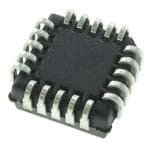
ICGOO电子元器件商城为您提供AD2S90APZ由Analog设计生产,在icgoo商城现货销售,并且可以通过原厂、代理商等渠道进行代购。 AD2S90APZ价格参考。AnalogAD2S90APZ封装/规格:数据采集 - ADCs/DAC - 专用型, R/D 转换器 12 b 串行 20-PLCC(9x9)。您可以下载AD2S90APZ参考资料、Datasheet数据手册功能说明书,资料中有AD2S90APZ 详细功能的应用电路图电压和使用方法及教程。
AD2S90APZ是Analog Devices Inc.(亚德诺半导体)生产的一款专用型数据采集芯片,主要应用于旋转编码器信号处理和解码。它属于数据采集系统中的ADCs/DACs(模数转换器/数模转换器)类别,具体为旋变数字转换器(Resolver-to-Digital Converter, RDC)。以下是AD2S90APZ的主要应用场景:

1. 电机控制:在工业自动化、机器人技术和伺服控制系统中,AD2S90APZ用于将旋转编码器的模拟输出信号转换为数字信号,从而精确测量电机转子的位置和速度。这有助于实现高精度的电机控制,确保系统的稳定性和响应速度。

2. 航空航天与国防:在飞行控制系统、雷达系统和导弹制导系统中,AD2S90APZ能够提供高精度的角度测量和位置反馈,确保系统的可靠性和安全性。其抗干扰能力强,适合恶劣环境下的应用。

3. 医疗设备:在医疗成像设备(如CT扫描仪、MRI设备)和手术机器人中,AD2S90APZ可以用于精确控制机械臂或移动部件的位置,确保操作的准确性和安全性。

4. 汽车电子:在电动汽车和混合动力汽车的动力传动系统中,AD2S90APZ用于监测电机转子的位置,帮助实现高效的能量管理和动力输出控制。此外,在自动驾驶系统中,它也用于精确的转向角和车轮位置检测。

5. 精密仪器:在高精度测量仪器和测试设备中,AD2S90APZ能够提供稳定可靠的信号转换,确保测量结果的准确性。例如,它可以用于光学仪器、激光测距仪等设备中。

总之,AD2S90APZ凭借其高性能和可靠性,广泛应用于对角度和位置精度要求极高的领域,特别是在需要实时反馈和高精度控制的应用场景中表现出色。
| 参数 | 数值 |
| 产品目录 | 集成电路 (IC)半导体 |
| 描述 | IC R/D CONV 12BIT 20-PLCC模数转换器 - ADC IC 12-Bit R/D Converter |
| 产品分类 | |
| 品牌 | Analog Devices Inc |
| 产品手册 | |
| 产品图片 |
|
| rohs | 符合RoHS无铅 / 符合限制有害物质指令(RoHS)规范要求 |
| 产品系列 | 数据转换器IC,模数转换器 - ADC,Analog Devices AD2S90APZ- |
| 数据手册 | |
| 产品型号 | AD2S90APZ |
| 产品目录页面 | |
| 产品种类 | 模数转换器 - ADC |
| 供应商器件封装 | 20-PLCC(9x9) |
| 分辨率 | 12 bit |
| 分辨率(位) | 12 b |
| 包装 | 管件 |
| 商标 | Analog Devices |
| 安装类型 | 表面贴装 |
| 安装风格 | SMD/SMT |
| 封装 | Tube |
| 封装/外壳 | 20-LCC(J 形引线) |
| 封装/箱体 | PLCC-20 |
| 工作温度 | -40°C ~ 85°C |
| 工作电源电压 | 5 V |
| 工厂包装数量 | 49 |
| 接口类型 | Serial |
| 数据接口 | 串行 |
| 最大工作温度 | + 85 C |
| 最小工作温度 | - 40 C |
| 标准包装 | 1 |
| 电压-电源 | ±4.75 V ~ 5.25 V |
| 电压源 | 双 ± |
| 类型 | R/D 转换器 |
| 系列 | AD2S90 |
| 结构 | Resolver to Digital |
| 输入类型 | Differential |
| 通道数量 | 1 Channel |
| 采样率(每秒) | - |


- 商务部:美国ITC正式对集成电路等产品启动337调查
- 曝三星4nm工艺存在良率问题 高通将骁龙8 Gen1或转产台积电
- 太阳诱电将投资9.5亿元在常州建新厂生产MLCC 预计2023年完工
- 英特尔发布欧洲新工厂建设计划 深化IDM 2.0 战略
- 台积电先进制程称霸业界 有大客户加持明年业绩稳了
- 达到5530亿美元!SIA预计今年全球半导体销售额将创下新高
- 英特尔拟将自动驾驶子公司Mobileye上市 估值或超500亿美元
- 三星加码芯片和SET,合并消费电子和移动部门,撤换高东真等 CEO
- 三星电子宣布重大人事变动 还合并消费电子和移动部门
- 海关总署:前11个月进口集成电路产品价值2.52万亿元 增长14.8%


PDF Datasheet 数据手册内容提取
a Low Cost, Complete 12-Bit Resolver-to-Digital Converter AD2S90 FEATURES FUNCTIONAL BLOCK DIAGRAM Complete Monolithic Resolver-to-Digital Converter Incremental Encoder Emulation (1024-Line) REF Absolute Serial Data (12-Bit) SIN SIN (u – f) Differential Inputs SIN LO HIGH ACCURACY P.S.D. AND VEL ANGLE SIN COS FREQUENCY 12-Bit Resolution COS u MULTIPLIER SHAPING ERROR Industrial Temperature Range COS LO DIGITAL AMPLIFIER 20-Lead PLCC ANGLE f U/D CLKOUT Low Power (50 mW) NMCA DECODE CUOP-UDNOTWENR CLK DYHNIGAMHIC B LOGIC RANGE V.C.O. DIR APPLICATIONS NM Industrial Motor Control CS LATCH Servo Motor Control Industrial Gauging SCLK SERIAL INTERFACE DATA Encoder Emulation Automotive Motion Sensing and Control Factory Automation Limit Switching GENERAL DESCRIPTION The AD2S90 operates on – 5 V dc – 5% power supplies and is The AD2S90 is a complete 12-bit resolution tracking resolver- fabricated on Analog Devices’ Linear Compatible CMOS pro- to-digital converter. No external components are required to cess (LC2MOS). LC2MOS is a mixed technology process that operate the device. combines precision bipolar circuits with low power CMOS logic The converter accepts 2 V rms – 10% input signals in the range circuits. 3kHz–20 kHz on the SIN, COS and REF inputs. A Type II servo loop is employed to track the inputs and convert the input PRODUCT HIGHLIGHTS SIN and COS information into a digital representation of the Complete Resolver-Digital Interface.The AD2S90 provides input angle. The bandwidth of the converter is set internally at the complete solution for digitizing resolver signals (12-bit reso- 1kHz within the tolerances of the device. The guaranteed maxi- lution) without the need for external components. mum tracking rate is 500 rps. Dual Format Position Data. Incremental encoder emulation Angular position output information is available in two forms, in standard A QUAD B format with selectable North Marker absolute serial binary and incremental A quad B. width. Absolute serial 12-bit angular binary position data accessed via simple 3-wire interface. The absolute serial binary output is 12-bit (1 in 4096). The data output pin is high impedance when Chip Select CS is logic HI. Single High Accuracy Grade in Low Cost Package. – 10.6 arc This allows the connection of multiple converters onto a com- minutes of angular accuracy available in a 20-lead PLCC. mon bus. Absolute angular information in serial pure binary Low Power. Typically 50mW power consumption. form is accessed by CS followed by the application of an exter- nal clock (SCLK) with a maximum rate of 2 MHz. The encoder emulation outputs A, B and NM continuously produce signals equivalent to a 1024 line encoder. When de- coded this corresponds to 12 bits of resolution. Three common north marker pulsewidths are selected via a single pin (NMC). An analog velocity output signal provides a representation of velocity from a rotating resolver shaft traveling in either a clock- wise or counterclockwise direction. REV. D Information furnished by Analog Devices is believed to be accurate and reliable. However, no responsibility is assumed by Analog Devices for its use, nor for any infringements of patents or other rights of third parties One Technology Way, P.O. Box 9106, Norwood, MA 02062-9106, U.S.A. which may result from its use. No license is granted by implication or Tel: 781/329-4700 World Wide Web Site: http://www.analog.com otherwise under any patent or patent rights of Analog Devices. Fax: 781/326-8703 © Analog Devices, Inc., 1999
AD2S90–SPECIFICATIONS (V = +5V 6 5%, V = –5V 6 5%, AGND = DGND = 0V, T = –408C to +858C unless DD SS A otherwise noted) Parameter Min Typ Max Units Test Condition SIGNAL INPUTS Voltage Amplitude 1.8 2.0 2.2 V rms Sinusoidal Waveforms, Differential SIN to SINLO, COS to COSLO Frequency 3 20 kHz Input Bias Current 100 nA V = 2 – 10% V rms IN Input Impedance 1.0 MW V = 2 – 10% V rms IN Common-Mode Volts1 100 mV peak CMV @ SINLO, COSLO w.r.t. CMRR 60 dB AGND @ 10 kHz REFERENCE INPUT Voltage Amplitude 1.8 2.0 3.35 V rms Sinusoidal Waveform Frequency 3 20 kHz Input Bias Current 100 nA Input Impedance 100 kW Permissible Phase Shift –10 +10 Degrees Relative to SIN, COS Inputs CONVERTER DYNAMICS Bandwidth 700 840 1000 Hz Maximum Tracking Rate 500 rps Maximum VCO Rate (CLKOUT) 2.048 MHz Settling Time 1(cid:176) Step 2 7 ms 179(cid:176) Step 20 ms ACCURACY Angular Accuracy2 – 10.6 + 1 LSB arc min Repeatability3 1 LSB VELOCITY OUTPUT Scaling 120 150 180 rps/V dc Output Voltage at 500 rps – 2.78 – 3.33 – 4.17 V dc Load Drive Capability – 250 m A V = – 2.5 V dc (typ), R ‡ 10 kW OUT L LOGIC INPUTS SCLK, CS Input High Voltage (V ) 3.5 V dc V = +5 V dc, V = –5 V dc INH DD SS Input Low Voltage (V ) 1.5 V dc V = +5 V dc, V = –5 V dc INL DD SS Input Current (I ) 10 m A IN Input Capacitance 10 pF LOGIC OUTPUTS DATA, A, B,4 NM, CLKOUT, DIR V = +5 V dc, V = –5 V dc DD SS Output High Voltage 4.0 V dc I = 1 mA OH Output Low Voltage 1.0 V dc I = 1 mA OL 0.4 V dc I = 400 m A OL SERIAL CLOCK (SCLK) SCLK Input Rate 2 MHz NORTH MARKER CONTROL (NMC) 90(cid:176) +4.75 +5.0 +5.25 V dc North Marker Width Relative to 180(cid:176) –0.75 DGND +0.75 V dc “A” Cycle 360(cid:176) –4.75 –5.0 –5.25 V dc POWER SUPPLIES V +4.75 +5.00 +5.25 V dc DD V –4.75 –5.00 –5.25 V dc SS I 10 mA DD I 10 mA SS NOTES 1If the tolerance on signal inputs = – 5%, then CMV = 200 mV. 21 LSB = 5.3 arc minute. 3Specified at constant temperature. 4Output load drive capability. Specifications subject to change without notice. –2– REV. D
AD2S90 (V = +5V 6 5%, V = –5V 6 5%, AGND = DGND = 0V, T = –408C to +858C unless TIMING CHARACTERISTICS1, 2 DD SS A otherwise noted) t2 t6 CSB t 3 SCLK t4 t* DATA MSB LSB t1 t t7 5 *THE MINIMUM ACCESS TIME: USER DEPENDENT Figure 1.Serial Interface NOTES 1Timing data are not 100% production tested. Sample tested at +25(cid:176)C only to ensure conformance to data sheet limits. Logic output timing tests carried out using 10 pF, 100 kW load. 2Capacitance of data pin in high impedance state = 15 pF. Parameter AD2S90 Units Test Conditions/Notes t 150 ns max CS to DATA Enable 1 t 1 600 ns min CS to 1st SCLK Negative Edge 2 t 250 ns min SCLK Low Pulse 3 t 250 ns min SCLK High Pulse 4 t 100 ns max SCLK Negative Edge to DATA Valid 5 t 600 ns min CS High Pulsewidth 6 t 150 ns max CS High to DATA High Z (Bus Relinquish) 7 NOTE 1SCLK can only be applied after t has elapsed. 2 A COUNTER IS CLOCKED ON THIS EDGE B CLKOUT tCLK t ABN 908 A, B, NM NM 1808 t DIR DIR 3608 NUMBER OF DEGREES REFERS TO WIDTH RELATIVE TO "A" CYCLE Figure 2.Incremental Encoder Figure 3.DIR/CLKOUT/A, B and NM Timing AD2S90 Parameter Min Max Units Test Conditions/Notes t 200 ns DIR to CLKOUT Positive Edge DIR t 250 400 ns CLKOUT Pulsewidth CLK t 250 ns CLKOUT Negative Edge to A, B and NM Transition ABN REV. D –3–
AD2S90 RECOMMENDED OPERATING CONDITIONS PIN DESCRIPTIONS Power Supply Voltage (V – V ) . . . . . . . . . . – 5 V dc – 5% DD SS Analog Input Voltage (SIN, COS & REF) . . . . .2 V rms – 10% Pin Signal and Reference Harmonic Distortion . . . . . . . . . . . .10% No. Mnemonic Function Phase Shift between Signal and Reference . . . . . . . . . . . . .– 10(cid:176) 1 AGND Analog ground, reference ground. Ambient Operating Temperature Range Industrial (AP) . . . . . . . . . . . . . . . . . . . . . . .–40(cid:176) C to +85(cid:176) C 2 SIN SIN channel noninverting input connect to resolver SIN HI output. SIN to SIN LO = 2 V rms – 10%. ABSOLUTE MAXIMUM RATINGS* V to AGND . . . . . . . . . . . . . . . . . . . .–0.3 V dc to +7.0 V dc 3 SIN LO SIN channel inverting input connect to DD V to AGND . . . . . . . . . . . . . . . . . . . .+0.3 V dc to –7.0 V dc resolver SIN LO. SS AGND to DGND . . . . . . . . . . . . –0.3 V dc to V + 0.3 V dc DD 4 DATA Serial interface data output. High impedance Analog Inputs to AGND with CS = HI. Enabled by CS = 0. REF . . . . . . . . . . . . . . . . . .V – 0.3 V dc to V + 0.3 V dc SS DD 5 SCLK Serial interface clock. Data is clocked out on SIN, SIN LO . . . . . . . . . . .V – 0.3 V dc to V + 0.3 V dc SS DD “first” negative edge of SCLK after a LO transi- COS, COS LO . . . . . . . . . .V – 0.3 V dc to V + 0.3 V dc SS DD tion on CS. 12 SCLK pulses to clock data out. Analog Output to AGND VEL . . . . . . . . . . . . . . . . . . . . . . . . . . . . . . . . . . .V to V 6 CS Chip select. Active LO. Logic LO transition SS DD Digital Inputs to DGND, CSB, enables DATA output. SCLK, RES . . . . . . . . . . . . . . . –0.3 V dc to V + 0.3 V dc DD 7 A Encoder A output. Digital Outputs to DGND, NM, A, B, DIR, CLKOUT DATA . . . . . . –0.3 V dc to V + 0.3 V dc 8 B Encoder B output. DD Operating Temperature Range 9 NM Encoder North Marker emulation output. Industrial (AP) . . . . . . . . . . . . . . . . . . . . . . .–40(cid:176) C to +85(cid:176) C Pulse triggered as code passes through zero. Storage Temperature Range . . . . . . . . . . . . .–65(cid:176) C to +150(cid:176) C Three common pulsewidths available. Lead Temperature (Soldering 10 sec) . . . . . . . . . . . . . . 300(cid:176) C 10 DIR Indicates direction of rotation of input. Power Dissipation to +75(cid:176) C . . . . . . . . . . . . . . . . . . . .300 mW Logic HI = increasing angular rotation. Derates above +75(cid:176) C by . . . . . . . . . . . . . . . . . . . . . 10mW/(cid:176) C Logic LO = decreasing angular rotation. *Stresses above those listed under Absolute Maximum Ratings may cause perma- 11 DGND Digital power ground return. nent damage to the device. This is a stress rating only; functional operation of the device at these or any other conditions above those indicated in the operational 12 V Negative power supply, –5 V dc – 5%. section of this specification is not implied. Exposure to absolute maximum rating SS conditions for extended periods may affect device reliability. 13 V Positive power supply, +5 V dc – 5%. DD ORDERING GUIDE 14 VDD Positive power supply, +5 V dc – 5%. Must be connected to Pin 13. Model Temperature Range Accuracy Package Option 15 NMC North marker width control. Internally pulled AD2S90AP –40(cid:176) C to +85(cid:176) C 10.6 arc min P-20A HI via 50 kW nominal. 16 CLKOUT Internal VCO clock output. Indicates angular velocity of input signals. Max nominal rate = PIN CONFIGURATION 1.536 MHz. CLKOUT is a 300 ns positive pulse. O 17 VEL Indicates angular velocity of input signals. N LO N GND OS OS L Positive voltage w.r.t. AGND indicates in- SI SI A C C creasing angle. FSD = 375 rps. 3 2 1 20 19 18 REF Converter reference input. Normally derived DATA 4 PIN 1 18 REF IDENTIFIER from resolver primary excitation. REF = 2 V SCLK 5 17 VEL AD2S90 rms nominal. Phase shift w.r.t. COS and SIN CS 6 TOP VIEW 16 CLKOUT = – 10(cid:176) max A 7 (Not to Scale) 15 NMC B 8 14 VDD 19 COS LO COS channel inverting input. Connect to resolver COS LO. 9 10 11 12 13 M R D S D 20 COS COS channel noninverting input. Connect to N DI GN VS VD resolver COS HI output. COS = 2 V rms – 10%. D CAUTION The AD2S90 features an input protection circuit consisting of large “distributed” diodes and polysilicon series resistors to dissipate both high energy discharges (Human Body Model) and WARNING! fast, low energy pulses (Charges Device Model). Proper ESD precautions are strongly recommended to avoid functional damage or performance degradation. For further information on ESD precautions, refer to Analog Devices ESD ESD SENSITIVE DEVICE Prevention Manual. –4– REV. D
AD2S90 RESOLVER FORMAT SIGNALS For more information on the operation of the converter, see A resolver is a rotating transformer which has two stator wind- Circuit Dynamics section. ings and one rotor winding. The stator windings are displaced mechanically by 90(cid:176) (see Figure 4). The rotor is excited with an ac reference. The amplitude of subsequent coupling onto the stator windings is a function of the position of the rotor (shaft) relative to the stator. The resolver, therefore, produces two S2 TO S4 (COS) output voltages (S3–S1, S2–S4) modulated by the SINE and COSINE of shaft angle. Resolver format signals refer to the signals derived from the output of a resolver. Equation 1 illus- S3 TO S1 trates the output form. (SIN) S3–S1 = E SIN w t • SINq O S2–S4 = EO SIN w t • COSq (1) R2 TO R4 (REF) where: q = shaft angle SIN w t = rotor excitation frequency E = rotor excitation amplitude O 08 908 1808 2708 3608 Principle of Operation u The AD2S90 operates on a Type 2 tracking closed-loop prin- Figure 4.Electrical and Physical Resolver Representation ciple. The output continually tracks the position of the resolver without the need for external convert and wait states. As the Connecting The Converter transducer moves through a position equivalent to the least Refer to Figure 4. Positive power supply VDD = +5V dc – 5% significant bit weighting, the output is updated by one LSB. should be connected to Pin 13 & Pin 14 and negative power supply V = –5 V dc – 5% to Pin 12. Reversal of these power On the AD2S90, CLKOUT updates corresponding to one LSB SS supplies will destroy the device. S3 (SIN) and S2 (COS) increment. If we assume that the current word state of the from the resolver should be connected to the SIN and COS pins up-down counter is f , S3–S1 is multiplied by COS f and S2–S4 of the converter. S1 (SIN) and S4 (COS) from the resolver is multiplied by SIN f to give: should be connected to the SINLO and COSLO pins of the E SIN w t • SIN q COSf converter. The maximum signal level of either the SIN or COS O E SIN w t • COS q SINf (2) resolver outputs should be 2 V rms – 10%. The AD2S90 O An error amplifier subtracts these signals giving: AGND pin is the point at which all analog signal grounds should be star connected. The SIN LO and COS LO pins on the E SIN q • (SIN q COS f – COS q SIN f) O AD2S90 should be connected to AGND. Separate screened or twisted cable pairs are recommended for all analog inputs SIN, E SIN w t • SIN (q – f) (3) COS, and REF. The screens should terminate at the converter O AGND pin. where (q – f ) = angular error North marker width selection is controlled by Pin 15, NMC. A phase sensitive detector, integrator and voltage controlled Application of V , 0V, or V to NMC will select standard DD SS oscillator (VCO) form a closed loop system which seeks to null 90(cid:176) , 180(cid:176) and 360(cid:176) pulsewidths. If unconnected, the NM pulse sin (q – f ). When this is accomplished the word state of the defaults to 90(cid:176) . For a more detailed description of the output up/down counter, f , equals within the rated accuracy of the formats available see the Position Output section. converter, the resolver shaft angle q . +5V OSCILLATOR 10nF 47mF 0V (POWER GROUND) 10nF 47mF 18 17 16 15 14 –5V REF VDD S4 TWISTED PAIR 19 COS LO VDD 13 SCREENED CABLE S2 20 COS VSS 12 1 AGND DGND 11 2 SIN 10 3 SIN LO 9 AD2S90AP S2 S4 4 5 6 7 8 R1 S3 S3 R2 S1 S1 RESOLVER POWER RETURN Figure 5.Connecting the AD2S90 to a Resolver REV. D –5–
AD2S90 ABSOLUTE POSITION OUTPUT The north marker pulse is generated as the absolute angular SERIAL INTERFACE position passes through zero. The AD2S90 supports the three Absolute angular position is represented by serial binary data industry standard widths controlled using the NMC pin. Figure and is extracted via a three-wire interface, DATA, CS and 7 details the relationship between A, B and NM. The width of SCLK. The DATA output is held in a high impedance state NM is defined relative to the A cycle. when CS is HI. Upon the application of a Logic LO to the CS pin, the DATA INCREASING ANGLE output is enabled and the current angular information is trans- ferred from the counters to the serial interface. Data is retrieved A by applying an external clock to the SCLK pin. The maximum data rate of the SCLK is 2MHz. To ensure secure data retrieval it is important to note that SCLK should not be applied until a B minimum period of 600 ns after the application of a Logic LO to CS. Data is then clocked out, MSB first, on successive nega- 908 tive edges of the SCLK; 12 clock edges are required to extract the full 12 bits of data. Subsequent negative edges greater than the defined resolution of the converter will clock zeros from the *NM 1808 data output if CS remains in a low state. If a resolution of less than 12 bits is required, the data access 3608 can be terminated by releasing CS after the required number of bits have been read. NUMBER OF DEGREES REFERS TO WIDTH RELATIVE TO "A" CYCLE t2 t6 *SELECTABLE WITH THREE - LEVEL LEVEL WIDTH CONTROL PIN "MARKER" DEFAULT +VDD 908 TO 908 USING INTERNAL PULL - UP. 0 1808 CSB –VSS 3608 t3 Figure 7.A, B and NM Timing SCLK Unlike incremental encoders, the AD2S90 encoder output is not subject to error specifications such as cycle error, eccentric- t4 t* ity, pulse and state width errors, count density and phase f . DATA MSB LSB The maximum speed rating, n, of an encoder is calculated from its maximum switching frequency, f , and its ppr (pulses per MAX t1 t t7 revolution). 5 *THE MINIMUM ACCESS TIME: USER DEPENDENT 60· f n= MAX Figure 6.Serial Read Cycle PPR CS can be released a minimum of 100 ns after the last negative The AD2S90 A, B pulses are initiated from CLKOUT which edge. If the user is reading data continuously, CS can be reap- has a maximum frequency of 2.048 MHz. The equivalent plied a minimum of 250 ns after it is released (see Figure 6). encoder switching frequency is: The maximum read time is given by: (12-bits read @ 2 MHz) 1/4 · 2.048MHz = 512 kHz (4 updates = 1 pulse) Max RD Time = [600 + (12 · 500) + 600 + 100] = 7.30m s. At 12 bits the ppr = 1024, therefore the maximum speed, n, of the AD2S90 is: INCREMENTAL ENCODER OUTPUTS The incremental encoder emulation outputs A, B and NM are 60· 512000 free running and are always valid, providing that valid resolver n= =30000rpm format input signals are applied to the converter. 1024 The AD2S90 emulates a 1024-line encoder. Relating this to This compares favorably with encoder specifications where f MAX converter resolution means one revolution produces 1024 A, B is specified from 20 kHz (photo diodes) to 125 kHz (laser based) pulses. B leads A for increasing angular rotation (i.e., clockwise depending on the light system used. A 1024 line laser-based direction). The addition of the DIR output negates the need for encoder will have a maximum speed of 7300 rpm. external A and B direction decode logic. DIR is HI for increas- The inclusion of A, B outputs allows the AD2S90 + resolver ing angular rotation. solution to replace optical encoders directly without the need to change or upgrade existing application software. –6– REV. D
AD2S90 VELOCITY OUTPUT unless all parts of the system are backed up, a reset to a known The analog velocity output VEL is scaled to produce 150 rps/V datum point needs to take place. This can be extremely hazard- dc – 15%. The sense is positive V dc for increasing angular ous in many applications. The AD2S90 gets round this problem rotation. VEL can drive a maximum load combination of by supplying an absolute position serial data stream upon re- 10 kW and 30 pF. The internal velocity scaling is fixed. quest, thus removing the need to reset to a known datum. POSITION CONTROL HOST I/O The rotor movement of dc or ac motors used for servo control is PORT TO HOST PROCESSOR COMMAND POSITION HOST monitored at all times. Feedback transducers used for this pur- SEQUENCER (32-BIT) INTERFACE pose detect either relative position in the case of an incremental + POWER encoder or absolute position and velocity using a resolver. An S DIGITAL 8 – 12 AMP incremental encoder only measures change in position not – PID DAC DAC actual position. (F1I6L-TBEITR) PORT DC MOTOR POSITION Closed Loop Control Systems FEEDBACK The primary demand for a change in position must take into PROCESSOR (32-BIT) account the magnitude of that change and the associated accel- OPTIONAL VELOCITY eration and velocity characteristics of the servo system. This is IN, A, B INCREMENTAL POSITION FEEDBACK necessary to avoid “hunting” due to over- or underdamping of AD2S90 the control employed. ABSOLUTE POSITION RESOLVER A position loop needs both actual and demand position infor- mation. Algorithms consisting of proportional, integral and Figure 9.Practical Implementation of the AD2S90 derivative control (PID) may be implemented to control the DSP Interfacing velocity profile. The AD2S90 serial output is ideally suited for interfacing to A simplified position loop is shown in Figure 8. DSP configured microprocessors. Figures 10 to 13 illustrate how to configure the AD2S90 for serial interfacing to the DSP. ADSP-2105 Interfacing POSITION CONTROLLER PDOESMITAIONND SAERMVPO MSEORTVOOR Fonig-uchreip 1 s0e rsihaol wpso rtth oe fA thDe2 AS9D0S iPn-t2e1rf0a5c eids utose adn i nA DalStePrn-2a1te0 5fr.a Tmh-e ing receive mode with internal framing (internally inverted) and internal serial clock generation (externally inverted) options PAOCSTIUTIAOLN AD2S90 SORLEV-ER selected. In this mode the ADSP-2105 provides a CS and a serial clock to the AD2S90. The serial clock is inverted to pre- vent timing errors as a result of both the AD2S90 and ADSP- Figure 8.Position Loop 2105 clock data on the negative edge of SCLK. The first data bit is void; 12 bits of significant data then follow on each con- MOTION CONTROL PROCESSES secutive negative edge of the clock. Data is clocked from the Advanced VLSI designs mean that silicon system blocks are now AD2S90 into the data receive register of the ADSP-2105. This available to achieve high performance motion control in servo is internally set to 13 bit (12 bits and one “dummy” bit) when systems. 13 bits are received. The serial port automatically generates an A digital position control system using the AD2S90 is shown in internal processor interrupt. This allows the ADSP-2105 to read Figure 9. In this system the task of determining the acceleration 12 significant bits at once and continue processing. and velocity characteristics is fulfilled by programming a trap- The ADSP-2101, ADSP-2102, ADSP-2111 and 21msp50 can ezoidal velocity profile via the I/O port. all interface to the AD2S90 with similar interface circuitry. As can be seen from Figure 9 encoder position feedback infor- mation is used. This is a popular format and one which the AD2S90 emulates thereby facilitating the replacement of encod- SCLK SCLK ers with an AD2S90 and a resolver. However, major benefits ADSP-2105 AD2S90 can be realized by adopting the resolver principle as opposed to RFS CS the incremental technique. DR DATA Incremental feedback based systems normally carry out a peri- odic check between the position demanded by the controller NOTE: ADDITIONAL PINS OMITTED FOR CLARITY and the increment position count. This requires software and hardware comparisons and battery backup in the case of power Figure 10. ADSP-2105/AD2S90 Serial Interface failure. If there is a supply failure and the drive system moves, REV. D –7–
AD2S90 TMS32020 Interfacing Select the AD2S90 and frame the data. The S1 register is fixed Figure 11 shows the serial interface between the AD2S90 and at 16 bits, therefore, to obtain the 12-significant bits the proces- the TMS32020. The interface is configured in alternate internal sor needs to execute four right shifts. Once the NEC7720 has framing, external clock (externally inverted) mode. Sixteen bits read 16 bits, an internal interrupt is generated to read the inter- of data are clocked from the AD2S90 into the data receive regis- nal contents of the S1 register. ter (DRR) of the TMS32020. The DRR is fixed at 16 bits. To obtain the 12-significant bits, the processor needs to execute three right shifts. (First bit read is void, the last three will be SCLK SCLK zeros). When 16 bits have been received by the TMS32020, it mPD7720 AD2S90 generates an internal interrupt to read the data from the DRR. SIEN CS S1 DATA SCLK SCLK NOTE: TMS32020 AD2S90 ADDITIONAL PINS OMITTED FOR CLARITY FSR CS Figure 13. m PD7720/AD2S90 Serial Interface DRR DATA EDGE TRIGGERED 43 DECODING LOGIC NOTE: In most data acquisition or control systems the A, B incremental ADDITIONAL PINS OMITTED FOR CLARITY outputs must be decoded into absolute information, normally a Figure 11.TMS32020/AD2S90 Serial Interface parallel word, before they can be utilized effectively. To decode the A, B outputs on the AD2S90 the user must DSP56000 Interface implement a 4· decoding architecture. The principle states that Figure 12 shows a serial interface between the AD2S90 and the one A, B cycle represents 4 LSB weighted increments of the DSP56000. The DSP in configured for normal mode synchro- converter (see Equation 4). nous operation with gated clock with SCLK and SC1 as out- puts. SC1 is applied to CS. Up = (› A) • B + (fl B) • A + (fl A) • B + (› B ) • A Down = (› A) • B + (› B) • A + (fl A) • B + (fl B) • A (4) SCLK SCLK DSP56000 AD2S90 CLOCKWISE ROTATION COUNTER CLOCKWISE ROTATION SC1 CS CH A SRD DATA NOTE: CH B ADDITIONAL PINS OMITTED FOR CLARITY Figure 12.DSP56000/AD2S90 Serial Interface The DSP56000 assumes valid data on the first falling edge of UP DOWN SCLK. SCLK is inverted to ensure that the valid data is clocked Figure 14.Principles of 4· Decoding in after one leading bit. The receive data shift register (SRD) is set for a 13-bit word. The algorithms in Equation 4 can be implemented using the architecture shown in Figure 15. Traditionally the direction of When this register has received 13 bits of data, it generates an the shaft is decoded by determining whether A leads B. The internal interrupt on the DSP56000 to read the 12 bits of sig- AD2S90 removes the need to derive direction by supplying a nificant data from the register. direction output state which can be fed straight into the up- NEC7720 Interface down counter. Figure 13 shows the serial interface between the NEC7720 and For further information on this topic please refer to the applica- the AD2S90. The NEC7720 expects data on the rising edge of tion note “Circuit Applications of the AD2S90 Resolver-to- its SCLK output, and therefore unlike the previous interfaces no Digital Converters.” inverter is required to clock data into the S1 register. There is no need to ignore the first data bit read. SIEN is used to Chip CHA A A EDGE GENERATOR B CHB B CLOCK UP/DOWN PARALLEL DIRECTION U/D COUNTER DIGITAL OUTPUT RESET Figure 15.4· Decoding Incremental to Parallel Conversion –8– REV. D
AD2S90 REMOTE MULTIPLE SENSOR INTERFACING The AD2S90 acceleration constant is given by: The DATA output of the AD2S90 is held in a high impedance state until CS is taken LO. This allows a user to operate the K a=K1· K2@ 3·.0 106sec- 2 (8) AD2S90 in an application with more than one converter con- The AD2S90’s design has been optimized with a critically nected on the same line. Figure 16 shows four resolvers inter- damped response. The closed-loop transfer function is given by: faced to four AD2S90s. Excitation for the resolvers is provided locally by an oscillator. q 1+st OUT = 1 SCLK, DATA and two address lines are fed down low loss q IN 1+st + s2 + s3t2 (9) cables suitable for communication links. The two address lines 1 K K K K 1 2 1 2 are decoded locally into CS for the individual converters. Data is received and transmitted using transmitters and receivers. The normalized gain and phase diagrams are given in Figures 18 A0 and 19. 2-4 DECODING (74HC139) 4 A1 5 RES1 AD2S90 CS1CS2CS3 CS4 1 0 4 RES2 AD2S90 –5 2 SCLK –10 4 RES3 AD2S90 DATA –15 3 4 –20 RES4 AD2S90 4 VDD –25 2 2 VSS –30 OSC 0V BUFFER –35 Figure 16.Remote Sensor Interfacing –40 CIRCUIT DYNAMICS/ERROR SOURCES –45 1 10 100 1k 10k Transfer Function FREQUENCY – Hz The AD2S90 operates as a Type 2 tracking servo loop. An Figure 18.AD2S90 Gain Plot integrator and VCO/counter perform the two integrations inher- ent in a Type 2 loop. 0 The overall system response of the AD2S90 is that of a unity –20 gain second order low-pass filter, with the angle of the resolver as the input and the digital position data as the output. Figure –40 17 illustrates the AD2S90 system diagram. –60 –80 VEL OUT u IN u OUT –100 A1 (S) A2 (S) –120 –140 Figure 17.AD2S90 Transfer Function –160 The open-loop transfer function is given by: –180 q K K (1+st ) 1 10 100 1k 10k OUT = 1 2 1 (5) FREQUENCY – Hz q IN s2 1+st2 Figure 19.AD2S90 Phase Plot where: K 1+st t =1.0ms A 1(s)= s11+st21 t 12=90m s (6) K K =4.875V/(LSB· sec) A(s)= 2 1 (7) 2 s K =614,400LSB/(V· sec) 2 REV. D –9–
AD2S90 The small step response is given in Figure 20, and is the time SOURCES OF ERROR taken for the converter to settle to within 1 LSB. Acceleration Error A tracking converter employing a Type 2 servo loop does not ts = 7.00 ms (maximum) suffer any velocity lag, however, there is an additional error due The large step response (steps >20(cid:176) ) applies when the error to acceleration. This additional error can be defined using the voltage will exceed the linear range of the converter. Typically it acceleration constant K of the converter. will take three times longer to reach the first peak for a 179(cid:176) a step. Input Acceleration In response to a velocity step [VELOUT/(dq /dt)] the velocity K a = ErrorinOutput Angle (10) output will exhibit the same response characteristics as outlined The numerator and denominator’s units must be consistent. K a above. does not define maximum input acceleration, only the error due to its acceleration. The maximum acceleration allowable before the converter loses track is dependent on the angular accuracy requirements of the system. 108 Angular Error · K = degrees/sec2 (11) a K can be used to predict the output position error for a given a input acceleration. The AD2S90 has a fixed K = 3.0 · 106 EES sec–2 if we apply an input accelerating at 100 reavs/sec2, the error R EG can be calculated as follows: D [ ] Input Acceleration LSB/sec2 Error inLSBs= [ ] 08 K sec- 2 a [ ] [ ] 100 rev/sec2 · 212 LSB/rev 0 4 8 12 16 20 = [ ] =0.14LSBs Figure 20.Small Step Response 3.0· 106 sec–2 (12) –10– REV. D
AD2S90 AD2S90/AD2S99 TYPICAL CONFIGURATION shields should also be terminated at the AD2S90 AGND pin. Figure 21 shows a typical circuit configuration for the AD2S99 The SYNREF output of the AD2S99 should be connected to Oscillator and the AD2S90 Resolver-to-Digital Converter. The the REF input pin of the AD2S90 via a 0.1 m F capacitor with a maximum level of the SIN and COS input signals to the 100 kW resistor to GND. This is to block out any dc offset in AD2S90 should be 2 V rms – 10%. All the analog ground sig- the SYNREF signal. For more detailed information please refer nals should be star connected to the AD2S90 AGND pin. If to the AD2S99 data sheet. shielded twisted pair cables are used for the resolver signals, the VSS 4.7mF 0.1mF FBIAS SEL1 SEL2 VSSVSS NC = NO CONNECT 3 2 1 20 19 EXC NC 4 18 SIN EXC 5 AD2S99 17 DGND 6 TOP VIEW 16 AGND COS (Not to Scale) 7 15NC SEL2 = GND NC 8 14 NC SEL1 = VSS FOUT = 5kHz 9 10 11 12 13 NCSYNREF LOS50VkDDV NC4.7mF VDD 0.1mF 0.1mF 100kV 18 17 16 15 14 VDD 4.7mF 0.1mF REF 19 COS LO VDD 13 4.7mF 0.1mF 20 COS VSS 12 VSS 1 AGND DGND 11 S2 COS S4 2 SIN AD2S90 10 R2 S3 3 SIN LO TOP VIEW 9 REF SIN (Not to Scale) 4 5 6 7 8 R4 S1 RESOLVER Figure 21.AD2S90 and AD2S99 Example Configuration REV. D –11–
AD2S90 OUTLINE DIMENSIONS Dimensions shown in inches and (mm). P-20A 20-Lead Plastic Leaded Chip Carrier (PLCC) 0.180 (4.57) 0.048 (1.21) 0.165 (4.19) 99 0.042 (1.07) 0.056 (1.42) 0.025 (0.63) –1/ 0.048 (1.21) 0.042 (1.07) 0.015 (0.38) b–2 0.042 (1.07) 3 19 0.021 (0.53) 53 4 IDEPNITNI F1IER18 0(1.0.2570) 0.013 (0.33)0.330 (8.38) C16 TOP VIEW BSC 0.032 (0.81)0.290 (7.37) (PINS DOWN) 0.026 (0.66) 8 14 9 13 0.020 0.040 (1.01) (0.50) 0.356 (9.04) R 0.350 (8.89)SQ 0.025 (0.64) 0.395 (10.02) 0.110 (2.79) 0.385 (9.78)SQ 0.085 (2.16) 0.020 (0.50) R PIN 1 IDENTIFIER BOTTOM VIEW (PINS UP) A. S. U. N D I E T N RI P –12– REV. D
Mouser Electronics Authorized Distributor Click to View Pricing, Inventory, Delivery & Lifecycle Information: A nalog Devices Inc.: AD2S90AP AD2S90APZ