ICGOO在线商城 > AC164133
 Datasheet下载
- 型号: AC164133
- 制造商: Microchip
- 库位|库存: xxxx|xxxx
- 要求:
| 数量阶梯 | 香港交货 | 国内含税 |
| +xxxx | $xxxx | ¥xxxx |
查看当月历史价格
查看今年历史价格
AC164133产品简介:
ICGOO电子元器件商城为您提供AC164133由Microchip设计生产,在icgoo商城现货销售,并且可以通过原厂、代理商等渠道进行代购。 提供AC164133价格参考以及MicrochipAC164133封装/规格参数等产品信息。 你可以下载AC164133参考资料、Datasheet数据手册功能说明书, 资料中有AC164133详细功能的应用电路图电压和使用方法及教程。
| 参数 | 数值 |
| 产品目录 | 编程器,开发系统半导体 |
| 描述 | PICTAIL PLUS BUCK/BOOST DB电源管理IC开发工具 dsPIC BuckBoost PICtail Daughtr Brd |
| 产品分类 | |
| 品牌 | Microchip Technology |
| 产品手册 | |
| 产品图片 |
|
| rohs | 符合RoHS无铅 / 符合限制有害物质指令(RoHS)规范要求 |
| 产品系列 | 电源管理IC开发工具,Microchip Technology AC164133PICtail™ Plus |
| 数据手册 | |
| 产品型号 | AC164133 |
| 主要用途 | DC/DC,步升/步降 |
| 产品 | Evaluation Boards |
| 产品目录页面 | |
| 产品种类 | 电源管理IC开发工具 |
| 使用的IC/零件 | PICtail™ Plus 板 |
| 功率-输出 | - |
| 商标 | Microchip Technology |
| 工具用于评估 | dsPIC33F |
| 工厂包装数量 | 1 |
| 所含物品 | 板 |
| 板类型 | 完全填充 |
| 标准包装 | 1 |
| 特色产品 | http://www.digikey.com/cn/zh/ph/microchip/dspic33f.html |
| 用于 | MA330020, MA330024, 28 pin starter development board |
| 电压-输入 | 7 V ~ 15 V |
| 电压-输出 | - |
| 电流-输出 | - |
| 稳压器拓扑 | 降压-升压 |
| 类型 | Voltage Regulators - Switching Regulators |
| 输入电压 | 7 V to 15 V |
| 输出和类型 | 3,非隔离 |
| 输出电压 | 3.3 V, 5 V, 20 V |
| 输出电流 | 750 mA, 3 A |
| 频率-开关 | - |


- 商务部:美国ITC正式对集成电路等产品启动337调查
- 曝三星4nm工艺存在良率问题 高通将骁龙8 Gen1或转产台积电
- 太阳诱电将投资9.5亿元在常州建新厂生产MLCC 预计2023年完工
- 英特尔发布欧洲新工厂建设计划 深化IDM 2.0 战略
- 台积电先进制程称霸业界 有大客户加持明年业绩稳了
- 达到5530亿美元!SIA预计今年全球半导体销售额将创下新高
- 英特尔拟将自动驾驶子公司Mobileye上市 估值或超500亿美元
- 三星加码芯片和SET,合并消费电子和移动部门,撤换高东真等 CEO
- 三星电子宣布重大人事变动 还合并消费电子和移动部门
- 海关总署:前11个月进口集成电路产品价值2.52万亿元 增长14.8%


PDF Datasheet 数据手册内容提取
Buck/Boost Converter PICtail™ Plus Daughter Board User’s Guide © 2008 Microchip Technology Inc. DS70336A
Note the following details of the code protection feature on Microchip devices: • Microchip products meet the specification contained in their particular Microchip Data Sheet. • Microchip believes that its family of products is one of the most secure families of its kind on the market today, when used in the intended manner and under normal conditions. • There are dishonest and possibly illegal methods used to breach the code protection feature. All of these methods, to our knowledge, require using the Microchip products in a manner outside the operating specifications contained in Microchip’s Data Sheets. Most likely, the person doing so is engaged in theft of intellectual property. • Microchip is willing to work with the customer who is concerned about the integrity of their code. • Neither Microchip nor any other semiconductor manufacturer can guarantee the security of their code. Code protection does not mean that we are guaranteeing the product as “unbreakable.” Code protection is constantly evolving. We at Microchip are committed to continuously improving the code protection features of our products. Attempts to break Microchip’s code protection feature may be a violation of the Digital Millennium Copyright Act. If such acts allow unauthorized access to your software or other copyrighted work, you may have a right to sue for relief under that Act. Information contained in this publication regarding device Trademarks applications and the like is provided only for your convenience The Microchip name and logo, the Microchip logo, Accuron, and may be superseded by updates. It is your responsibility to dsPIC, KEELOQ, KEELOQ logo, MPLAB, PIC, PICmicro, ensure that your application meets with your specifications. PICSTART, rfPIC and SmartShunt are registered trademarks MICROCHIP MAKES NO REPRESENTATIONS OR of Microchip Technology Incorporated in the U.S.A. and other WARRANTIES OF ANY KIND WHETHER EXPRESS OR countries. IMPLIED, WRITTEN OR ORAL, STATUTORY OR OTHERWISE, RELATED TO THE INFORMATION, FilterLab, Linear Active Thermistor, MXDEV, MXLAB, INCLUDING BUT NOT LIMITED TO ITS CONDITION, SEEVAL, SmartSensor and The Embedded Control Solutions QUALITY, PERFORMANCE, MERCHANTABILITY OR Company are registered trademarks of Microchip Technology FITNESS FOR PURPOSE. Microchip disclaims all liability Incorporated in the U.S.A. arising from this information and its use. Use of Microchip Analog-for-the-Digital Age, Application Maestro, CodeGuard, devices in life support and/or safety applications is entirely at dsPICDEM, dsPICDEM.net, dsPICworks, dsSPEAK, ECAN, the buyer’s risk, and the buyer agrees to defend, indemnify and ECONOMONITOR, FanSense, In-Circuit Serial hold harmless Microchip from any and all damages, claims, Programming, ICSP, ICEPIC, Mindi, MiWi, MPASM, MPLAB suits, or expenses resulting from such use. No licenses are Certified logo, MPLIB, MPLINK, mTouch, PICkit, PICDEM, conveyed, implicitly or otherwise, under any Microchip PICDEM.net, PICtail, PIC32 logo, PowerCal, PowerInfo, intellectual property rights. PowerMate, PowerTool, REAL ICE, rfLAB, Select Mode, Total Endurance, UNI/O, WiperLock and ZENA are trademarks of Microchip Technology Incorporated in the U.S.A. and other countries. SQTP is a service mark of Microchip Technology Incorporated in the U.S.A. All other trademarks mentioned herein are property of their respective companies. © 2008, Microchip Technology Incorporated, Printed in the U.S.A., All Rights Reserved. Printed on recycled paper. Microchip received ISO/TS-16949:2002 certification for its worldwide headquarters, design and wafer fabrication facilities in Chandler and Tempe, Arizona; Gresham, Oregon and design centers in California and India. The Company’s quality system processes and procedures are for its PIC® MCUs and dsPIC® DSCs, KEELOQ® code hopping devices, Serial EEPROMs, microperipherals, nonvolatile memory and analog products. In addition, Microchip’s quality system for the design and manufacture of development systems is ISO 9001:2000 certified. DS70336A-page ii © 2008 Microchip Technology Inc.
BUCK/BOOST CONVERTER PICtail™ PLUS DAUGHTER BOARD USER’S GUIDE Table of Contents Preface ...........................................................................................................................1 Chapter 1. Introduction 1.1 Overview ........................................................................................................7 1.2 Features .......................................................................................................11 1.3 Product Package ..........................................................................................11 Chapter 2. Hardware Overview 2.1 Daughter Board Connectors .........................................................................13 2.2 Daughter Board User Hardware Interface ....................................................15 2.3 Using the Daughter Board with the Explorer 16 Development Board ..........20 2.4 Using the Daughter Board with the 16-bit 28-pin Starter Development Board ................................................................................21 2.5 Power Rating of Converter Stage .................................................................24 Chapter 3. Getting Started 3.1 Overview ......................................................................................................25 3.2 Creating the Project ......................................................................................26 3.3 Building the Code .........................................................................................34 3.4 Programming the Device ..............................................................................38 3.5 Debugging the Code ....................................................................................44 Chapter 4. Demonstration Program Operation 4.1 Program Demonstration ...............................................................................49 4.2 Code Demonstration ....................................................................................51 4.3 Other Code Examples ..................................................................................51 Index .............................................................................................................................59 Worldwide Sales and Service ....................................................................................60 © 2008 Microchip Technology Inc. DS70336A-page iii
Buck/Boost Converter PICtail™ Plus Daughter Board User’s Guide NOTES: DS70336A-page iv © 2008 Microchip Technology Inc.
BUCK/BOOST CONVERTER PICtail™ PLUS DAUGHTER BOARD USER’S GUIDE Preface NOTICE TO CUSTOMERS All documentation becomes dated, and this manual is no exception. Microchip tools and documentation are constantly evolving to meet customer needs, so some actual dialogs and/or tool descriptions may differ from those in this document. Please refer to our web site (www.microchip.com) to obtain the latest documentation available. Documents are identified with a “DS” number. This number is located on the bottom of each page, in front of the page number. The numbering convention for the DS number is “DSXXXXXA”, where “XXXXX” is the document number and “A” is the revision level of the document. For the most up-to-date information on development tools, see the MPLAB® IDE on-line help. Select the Help menu, and then Topics to open a list of available on-line help files. INTRODUCTION This chapter contains general information that will be useful to know before using the Chapter Name. Items discussed in this chapter include: • Document Layout • Conventions Used in this Guide • Warranty Registration • Recommended Reading • The Microchip Web Site • Development Systems Customer Change Notification Service • Customer Support • Document Revision History DOCUMENT LAYOUT This document describes how to use the Buck/Boost Converter PICtail Plus Daughter Board as a development tool to emulate and debug firmware on a target board. The manual layout is as follows: • Chapter 1.“Introduction” – This chapter describes the Buck/Boost Converter PICtail Plus Daughter Board and provides a brief description of the hardware. • Chapter 2.“Hardware Overview” – This chapter describes the Buck/Boost Converter PICtail Plus Daughter Board hardware. • Chapter 3.“Getting Started” – This chapter describes the step-by-step process for getting your Buck/Boost Converter PICtail Plus Daughter Board up and running with the MPLAB® In-Circuit Debugger 2 (ICD 2) using a dsPIC33FJ16GS502 device. © 2008 Microchip Technology Inc. DS70336A-page 1
Buck/Boost Converter PICtail™ Plus Daughter Board User’s Guide • Chapter 4.“Demonstration Program Operation” – This chapter describes the operation of the Buck/Boost Converter PICtail Plus Daughter Board. • Appendix A.“Schematics and Layouts” – This appendix illustrates the Buck/Boost Converter PICtail Plus Daughter Board layout and provides hardware schematic diagrams. CONVENTIONS USED IN THIS GUIDE This manual uses the following documentation conventions: DOCUMENTATION CONVENTIONS Description Represents Examples Arial font: Italic characters Referenced books MPLAB® IDE User’s Guide Emphasized text ...is the only compiler... Initial caps A window the Output window A dialog the Settings dialog A menu selection select Enable Programmer Quotes A field name in a window or “Save project before build” dialog Underlined, italic text with A menu path File>Save right angle bracket Bold characters A dialog button Click OK A tab Click the Power tab N‘Rnnnn A number in Verilog format, 4‘b0010, 2‘hF1 where N is the total number of digits, R is the radix and n is a digit. Text in angle brackets < > A key on the keyboard Press <Enter>, <F1> Courier New font: Plain Courier New Sample source code #define START Filenames autoexec.bat File paths c:\mcc18\h Keywords _asm, _endasm, static Command-line options -Opa+, -Opa- Bit values 0, 1 Constants 0xFF, ‘A’ Italic Courier New A variable argument file.o, where file can be any valid filename Square brackets [ ] Optional arguments mcc18 [options] file [options] Curly brackets and pipe Choice of mutually exclusive errorlevel {0|1} character: { | } arguments; an OR selection Ellipses... Replaces repeated text var_name [, var_name...] Represents code supplied by void main (void) user { ... } DS70336A-page 2 © 2008 Microchip Technology Inc.
Preface WARRANTY REGISTRATION Please complete the enclosed Warranty Registration Card and mail it promptly. Sending in the Warranty Registration Card entitles users to receive new product updates. Interim software releases are available at the Microchip web site. RECOMMENDED READING This user's guide describes how to use the Chapter Name. Other useful documents are listed below. The following Microchip documents are available and recommended as supplemental reference resources. Readme for Chapter Name For the latest information on using Chapter Name, read the “Readme.txt” (an ASCII text file) in the Readme subdirectory of the MPLAB IDE installation directory from the Buck/Boost Converter PICtail Plus Daughter Board CD. The Readme file contains update information and known issues that may not be included in this user’s guide. Readme Files For the latest information on using other tools, read the tool-specific Readme files in the Readme subdirectory of the MPLAB IDE installation directory. The Readme files contain updated information and known issues that may not be included in this user’s guide. © 2008 Microchip Technology Inc. DS70336A-page 3
Buck/Boost Converter PICtail™ Plus Daughter Board User’s Guide THE MICROCHIP WEB SITE Microchip provides online support via our web site at www.microchip.com. This web site is used as a means to make files and information easily available to customers. Accessible by using your favorite Internet browser, the web site contains the following information: • Product Support – Data sheets and errata, application notes and sample programs, design resources, user’s guides and hardware support documents, latest software releases and archived software • General Technical Support – Frequently Asked Questions (FAQs), technical support requests, online discussion groups, Microchip consultant program member listing • Business of Microchip – Product selector and ordering guides, latest Microchip press releases, listing of seminars and events, listings of Microchip sales offices, distributors and factory representatives DEVELOPMENT SYSTEMS CUSTOMER CHANGE NOTIFICATION SERVICE Microchip’s customer notification service helps keep customers current on Microchip products. Subscribers will receive e-mail notification whenever there are changes, updates, revisions or errata related to a specified product family or development tool of interest. To register, access the Microchip web site at www.microchip.com, click on Customer Change Notification and follow the registration instructions. The Development Systems product group categories are: • Compilers – The latest information on Microchip C compilers and other language tools. These include the MPLAB C18 and MPLAB C30 C compilers; MPASM™ and MPLAB ASM30 assemblers; MPLINK™ and MPLAB LINK30 object linkers; and MPLIB™ and MPLAB LIB30 object librarians. • Emulators – The latest information on Microchip in-circuit emulators.This includes the MPLAB ICE 2000, MPLAB ICE 4000, and MPLAB REAL ICE™ in-circuit emulator. • In-Circuit Debuggers – The latest information on the Microchip in-circuit debugger, MPLAB ICD 2. • MPLAB IDE – The latest information on Microchip MPLAB IDE, the Windows® Integrated Development Environment for development systems tools. This list is focused on the MPLAB IDE, MPLAB SIM simulator, MPLAB IDE Project Manager and general editing and debugging features. • Programmers – The latest information on Microchip programmers. These include the MPLAB PM3 and PRO MATE II device programmers and the PICSTART® Plus and PICkit™ 1 development programmers. DS70336A-page 4 © 2008 Microchip Technology Inc.
Preface CUSTOMER SUPPORT Users of Microchip products can receive assistance through several channels: • Distributor or Representative • Local Sales Office • Field Application Engineer (FAE) • Technical Support Customers should contact their distributor, representative or field application engineer (FAE) for support. Local sales offices are also available to help customers. A listing of sales offices and locations is included in the back of this document. Technical support is available through the web site at: http://support.microchip.com DOCUMENT REVISION HISTORY Revision A (August 2008) This is the initial release of this document. © 2008 Microchip Technology Inc. DS70336A-page 5
Buck/Boost Converter PICtail™ Plus Daughter Board User’s Guide NOTES: DS70336A-page 6 © 2008 Microchip Technology Inc.
BUCK/BOOST CONVERTER PICtail™ PLUS DAUGHTER BOARD USER’S GUIDE Chapter 1. Introduction Modern power supplies are becoming smaller, more efficient, more flexible and less expensive. These desirable enhancements have come about as digital signal controllers are incorporated into Switch Mode Power Supply (SMPS) designs. Buck converters are used when the desired output voltage is smaller than the input voltage. Boost converters are used when the desired output voltage is higher than the input voltage. This chapter introduces and provides an overview of the Buck/Boost Converter PICtail Plus Daughter Board. The following topics are included in this chapter: • Overview • Features • Product Package 1.1 OVERVIEW The Buck/Boost Converter PICtail Plus Daughter Board (also referred to as Daughter Board) is a power supply board. It consists of two independent DC/DC synchronous buck converters and one independent DC/DC boost converter. Figure1-1 illustrates a block diagram of the Daughter Board. All of the necessary power, drive and control signals are available in the J1 and J2 con- nectors. The 16-bit 28-pin Starter Development Board can be used to control one inde- pendent DC/DC synchronous buck converters. This board can also control two buck stages, or one buck and one boost stage with hardware modification on the 16-bit 28-pin Starter Development Board. Refer to Section2.4.2“16-bit 28-pin Starter Development Board Controls Buck 1 and Boost Stages” for more details. The block diagram of the Daughter Board using the 16-bit 28-pin Starter Development Board is shown in Figure1-2. All three stages of the Buck/Boost Converter PICtail Plus Daughter Board are controlled by the Explorer 16 Development Board. Figure1-3 shows a block diagram of the Daughter Board using the Explorer 16 Development Board. The control boards provide closed-loop Proportional-Integral-Derivative (PID) control in the software to maintain the desired output voltage level. The dsPIC® DSC device provides the necessary memory and peripherals for A/D conversion, PWM generation, analog comparison and general purpose I/O, excluding the need to perform these func- tions in external circuitry. SMPS dsPIC® DSC devices are specifically designed to provide low-cost and efficient control for a wide range of power supply topologies. The specialized peripherals facilitate closed-loop feedback control of switch mode power supplies, providing communication for remote monitoring and supervisory control. The Daughter Board enables the end user to easily transition from analog-to-digital implementation of the power application. The Daughter Board also aids in rapid development of buck converter, boost converter, multi-phase buck converter and two parallel buck converters. © 2008 Microchip Technology Inc. DS70336A-page 7
Buck/Boost Converter PICtail™ Plus Daughter Board User’s Guide The dsPIC33F SMPS family of devices provides the following features: • Integrated program and data memory on a single chip • Ultra-fast interrupt response time and hardware interrupt priority logic • Up to 4 Msps, on-chip ADC with two SARs, and up to four dedicated and two shared sample/hold circuits for multiple loop control • Four independent, high-resolution PWM generators specially designed to support different power topologies • Four analog comparators for control loop implementation and system protection • On-chip system communications (I2C™/SPI/UART) • On-chip Fast RC oscillator for lower system cost • High-current sink/source for PWM pins: 16 mA/16 mA • CPU performance: 40 MIPS • Extensive power saving • CodeGuard™ Security enabled FIGURE 1-1: DAUGHTER BOARD BLOCK DIAGRAM VINSENSE VIN VIN LOAD AN4 AN4 VOUT1 I1 PWM1H I1 VIN AN0 AN0 V1 V1 AN1 AN1 PWM1L R J2 PWM1H R J1 LOAD O O T T EC EC GND N PWM1L N N N O O C C T T U U INP I2 INP VIN VOUT2 AN2 AN2 PWM2H I2 V2 AN3 AN3 V2 PWM2H PWM2L PWM2L Load VIN VOUT3 I3 AN8 V3 AN9 PWM3H PWM3H V3 I3 DS70336A-page 8 © 2008 Microchip Technology Inc.
Introduction FIGURE 1-2: 16-BIT 28-PIN STARTER DEVELOPMENT BOARD WITH DAUGHTER BOARD VIN VIN LOAD VOUT1 AN4 PWM1H I1 VDD VIN V1 PWM1H PWM1L D PWM1L R A O LOAD B T AN0 I1 N E GND M OP AN1 V1 L E V Load E PWM3L D R VIN VOUT2 E T PWM2H R TA PWM2H I2 S PWM2L N PI V2 8- BIT 2 AN2 I2 PWM2L - 6 1 AN3 V2 © 2008 Microchip Technology Inc. DS70336A-page 9
Buck/Boost Converter PICtail™ Plus Daughter Board User’s Guide FIGURE 1-3: EXPLORER 16 DEVELOPMENT BOARD WITH DAUGHTER BOARD VIN AN4 VIN LOAD VOUT1 VDD VIN PWM1H I1 PWM1H V1 D PWM1L PWM1L R A O B T I1 LOAD N AN0 E M P O V1 GND L AN1 E V E D Load 6 PWM3L VIN 1 R E R O PWM2H PWM2H I2 L P X E V2 PWM2L PWM2L I2 AN2 V2 AN3 VIN VOUT3 V3 PWM3H PWM3H I3 AN8 I3 V3 AN9 DS70336A-page 10 © 2008 Microchip Technology Inc.
Introduction 1.2 FEATURES The Buck/Boost Converter PICtail Plus Daughter Board provides the following features: 1.2.1 Power Stages • Two synchronous buck converter power stages • One boost converter power stage • Voltage/current measurement for digital control of buck converters • Voltage/current measurement for digital control of boost converter • Switchable, one 5Ω/5W resistive load on Buck Converter 1 output (VOUT1) • Buck Converter 1 output (VOUT1) on J4 connector for external loading • Buck Converter 2 output (VOUT2) on J5 connector for external loading • Boost Converter output (VOUT3) on J8 connector for external loading • Connector J9 for auxiliary power input 1.2.2 Additional Features • 5kΩ Potentiometer (RP1) connected via jumper J10 • Input voltage source selection via jumper J6 • Additional resistive load R46 via jumper J11 • Connectors J1 and J2 (Explorer 16/16-bit 28-pin Starter Development Board) • PMBus™ Connector (J3) 1.2.3 Daughter Board Power • Auxiliary power input (J9): +7V to +15V (+9V nominal) • 9V power input is through input connectors J2 and J1 • LED power-on indicator (D14) • LED output voltage indicators (D11, D12 and D13) Note: 9V input is supplied from the controller card (16-bit 28-pin Starter Development Board or Explorer 16 Development Board). All 16-bit 28-pin Starter Development Boards should have a blue wire connecting Pin 1 of J1 to Pin 28 of J2. If no blue wire connects them, connect a wire between them to supply the 9V input to the Buck/Boost Converter PICtail Plus Daughter Board. 1.3 PRODUCT PACKAGE The Buck/Boost Converter PICtail Plus Daughter Board kit consists of the following items: • Buck/Boost Converter PICtail Plus Daughter Board • Buck/Boost Converter PICtail Plus Daughter Board CD The CD consists of the application software, example code, Readme file and User’s Guide. © 2008 Microchip Technology Inc. DS70336A-page 11
Buck/Boost Converter PICtail™ Plus Daughter Board User’s Guide NOTES: DS70336A-page 12 © 2008 Microchip Technology Inc.
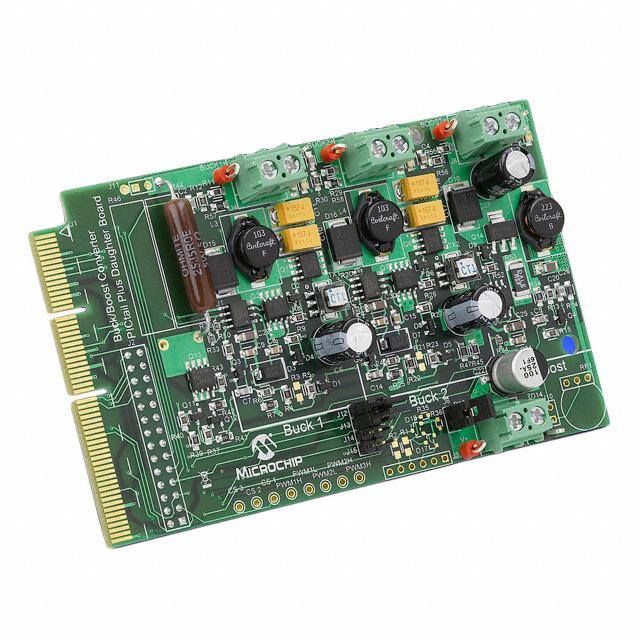
BUCK/BOOST CONVERTER PICtail™ PLUS DAUGHTER BOARD USER’S GUIDE Chapter 2. Hardware Overview This chapter lists and describes the hardware elements and components of the Buck/Boost Converter PICtail Plus Daughter Board (also referred to as Daughter Board). The following topics are included: • Daughter Board Connectors • Using the Daughter Board with the Explorer 16 Development Board • Using the Daughter Board with the 16-bit 28-pin Starter Development Board • Power Rating of Converter Stage • Power Rating of Converter Stage 2.1 DAUGHTER BOARD CONNECTORS The Daughter Board consists of different power sections along with the input and output connectors for signal and power connections. Figure2-1 depicts the Daughter Board, the input and output connectors and their locations. FIGURE 2-1: BUCK/BOOST CONVERTER PICtail™ PLUS DAUGHTER BOARD 4 5 6 1 2 7 3 1. J1 – To connect Explorer 16 Development Board 5. J5 – VOUT2 connector 2. J2 – To connect 16-bit 28-pin Starter Development Board 6. J8 – VOUT3 connector 3. J3 – PMBus™ interface connector 7. J9 – Auxiliary input power connector 4. J4 – VOUT1 connector © 2008 Microchip Technology Inc. DS70336A-page 13
Buck/Boost Converter PICtail™ Plus Daughter Board User’s Guide Note: The Daughter Board only consists of the three power trains of the DC/DC converter sections. Either the 16-bit 28-pin Starter Development Board with the dsPIC33FJ16GS502 device, or the Explorer 16 Development Board with the dsPIC33FJ16GS504 device can be used to control the DC/DC power sections of the Daughter Board. The J1 and J2 connectors provide the necessary signals for control purposes. 2.2 DAUGHTER BOARD USER HARDWARE INTERFACE This section describes the hardware interface of the Daughter Board and the power rating of each converter’s section. Figure2-2 displays the hardware elements (pin headers, jumpers, LED and potentiometer). FIGURE 2-2: BUCK/BOOST CONVERTER PICtail™ PLUS DAUGHTER BOARD HARDWARE ELEMENTS J11 D11 D12 D13 J1 J2 J6 D14 J10 RP1 2.2.1 Auxiliary Input Power Connector The Daughter Board can be connected to the auxiliary/bench power DC source through the J9 input connector. Jumper J6 should be removed while working with the auxiliary/bench power DC source. See FigureA-5 for the location of this jumper. 2.2.2 PMBus Interface Connector J3 The Daughter Board allows the user to implement the PMBus on the SMPS dsPIC DSC device using the J3 connector. See FigureA-6 for the location of this jumper. DS70336A-page 14 © 2008 Microchip Technology Inc.
Hardware Overview 2.2.3 16-bit 28-pin Starter Development Board Connector J2 The two converter stage sections of the Daughter Board can be controlled using the 16-bit 28-pin Starter Development Board. Table2-1 lists all of the power and signal connections on the Daughter Board J2 connector to the user interface with the 16-bit 28-pin Starter Development Board. See FigureA-6 for the location of this connector. TABLE 2-1: SIGNAL AND POWER CONNECTION FOR 16-BIT 28-PIN STARTER DEVELOPMENT BOARD (J2) Pin Number Assignment Primary Use Primary 1 NC Not Connected 2 AN0 Analog Input 0 (Buck Converter 1 current) 3 AN1 Analog Input 1 (Buck Converter 1 voltage) 4 AN2 Analog Input 2 (Buck Converter 2 current) 5 AN3 Analog Input 3 (Buck Converter 2 voltage) 6 AN4 Analog Input 4 (Input Voltage) 7 NC Not Connected 8 VSS Ground reference for logic and I/O pins 9 NC Not Connected 10 NC Not Connected 11 NC Not Connected 12 NC Not Connected 13 VDD Positive supply for logic and I/O pins 14 NC Not Connected 15 RB15 PMBUSAUX2 16 RB5 PMBUSAUX1 17 SCL SCL/TX 18 SDA SCL/RX 19 VSS Ground reference for logic and I/O pins 20 VDD +3.3V_DIG 21 PWM3H PWM Boost Converter 22 I/O Load 23 PWM2H PWM 2 High Output (Buck Converter 2) 24 PWM2L PWM 2 Low Output (Buck Converter 2) 25 PWM1H PWM 1 High Output (Buck Converter 1) 26 PWM1L PWM 1 Low Output (Buck Converter 1) 27 NC Not Connected 28 +9V Input Voltage for two buck stages © 2008 Microchip Technology Inc. DS70336A-page 15
Buck/Boost Converter PICtail™ Plus Daughter Board User’s Guide 2.2.4 Explorer 16 Development Board Connector J1 The two buck sections and one boost section of the Daughter Board can be controlled using the Explorer 16 Development Board. Table2-2 lists all the power and signal connections on the Daughter Board J1 connector to the user interface with the Explorer 16 Development Board. See FigureA-6 for the location of this connector. TABLE 2-2: SIGNAL AND POWER CONNECTION FOR THE EXPLORER 16 DEVELOPMENT BOARD (J1) Pin Number Assignment Primary Use Primary 79 AN0 Analog Input 0 (Buck Converter 1 current) 80 AN1 Analog Input 1 (Buck Converter 1 voltage) 45 PWM1H PWM 1 High Output (Buck Converter 1 drive) 46 PWM1L PWM 1 Low Output (Buck Converter 1 drive) 8 AN2 Analog Input 2 (Buck Converter 2 current) 6 AN3 Analog Input 3 (Buck Converter 2 voltage) 12 PWM2H PWM 2 High Output (Buck Converter 2 drive) 11 PWM2L PWM 2 Low Output (Buck Converter 2 drive) 50 AN4 Analog Input 4 (Input Voltage) 102 AN8 Analog Input 8 (Boost Converter Voltage) 80 AN9 Analog Input 9 (Boost Converter Voltage) 17 PWM3H PWM3H High Output (Boost Converter drive) 13 I/O Load Drive for Buck Converter 1 Load 101 AN10 Analog Input 10 (POT RP1) 65 RB15 PMBUSAUX2 66 RB5 PMBUSAUX1 67 SCL SCL/TX 68 SDA SCL/RX 9, 10, 119, 120 3.3VDIG_GND Ground Reference for Digital I/O pins 21, 22, 53, 54, +3.3V_DIG Digital 3.3V 107, 108 15, 16, 41, 42 9VANA_GND Ground Reference for Logic and I/O pins 25, 26, 57, 58 +9V 9V Input Voltage 1-5, 14, 18-20, 23, NC Not Connected 24, 27-30, 33-40, 43, 44, 49, 51, 52, 55, 56, 59-62, 69-78, 81-95, 97-100, 103-106, 109-118 DS70336A-page 16 © 2008 Microchip Technology Inc.
Hardware Overview 2.2.5 VOUT1 J4 (Buck1+) An external load can be connected to VOUT1 through the J4 connector. One on-board parallel resistor, R44 (5Ω/5W), is connected at the output of VOUT1 through MOSFET Q13 to optionally load the Buck 1 converter circuit. Resistor R45 is on-board, and there is space to solder resistor R46 onto the board. When resistor R46 is connected to VOUT1, the J11 jumper must be open while working with +9V power from the control board. The on-board load resistor can be connected to VOUT1 by controlling the signal name “Load”. The “Load” signal is the I/O pin of the SMPS dsPIC DSC device, and is active-high. See FigureA-2 for the location of this connector. 2.2.6 VOUT2 J5 (Buck2+) An external load can be connected to VOUT2 through the J5 connector. VOUT2 can load up to a maximum of 3 amps when the auxiliary input voltage source is connected at the J9 input connector. See FigureA-3 for the location of this connec- tor. 2.2.7 VOUT3 J8 (Boost) An external load can be connected to VOUT3 through the J8 connector. VOUT3 can load up to 0.75 amps when the auxiliary input voltage source is connected at the J9 input connector. See FigureA-4 for the location of this connector. 2.2.8 Jumpers The Daughter Board consists of three jumpers that determine its features. Table2-3 lists jumpers and their functions. TABLE 2-3: JUMPERS Jumpers Description Default Configurations J6 Select either 9V power provided by the Explorer 16 Develop- Short with jumper header (closed) ment Board or 16-bit 28-pin Starter Development Board, and an external power supply J10 Connects potentiometer RP1 to AN10 on Explorer 16 Develop- Open ment Board J11 Connects R46 load resistor to VOUT1 Open J12 Buck 2 voltage feedback selection Short with jumper header (closed) J13 Buck 2 current feedback selection Short with jumper header (closed) J14 Boost current feedback selection Open J15 Boost voltage feedback selection Open 2.2.9 Potentiometer and LED The Daughter Board consists of a potentiometer and LEDs for the user application. Table2-4 lists components and their functions. TABLE 2-4: POTENTIOMETERS AND LED Label Hardware Elements RP1 Potentiometer connected to AN10 of Explorer 16 Development Board controller D11 Buck 1 output LED D12 Buck 2 output LED D13 Boost output voltage LED D14 Input voltage LED © 2008 Microchip Technology Inc. DS70336A-page 17
Buck/Boost Converter PICtail™ Plus Daughter Board User’s Guide 2.2.10 Test Points The Daughter Board provides the various test points of the PWM signals, feedback signals and input and output voltages for the user application. Table2-5 lists the PWM test points that can be used to check the PWM gate pulse for all three power stages. TABLE 2-5: PWM TEST POINTS Test Points Description PWM1H Buck MOSFET gate drive of Buck 1 converter stage PWM1L Synchronous MOSFET gate drive of Buck 1 converter stage PWM2H Buck MOSFET gate drive of Buck 2 converter stage PWM2L Synchronous MOSFET gate drive of Buck 2 converter stage PWM3H Boost MOSFET gate drive for Boost converter stage Table2-6 lists the feedback signal test points that can be used to check the feedback signal waveforms and values. TABLE 2-6: FEEDBACK SIGNAL TEST POINTS Test Points Description Current Sense1 Current feedback signal for Buck 1 converter stage Current Sense2 Current feedback signal for Buck 2 converter stage Current Sense3 Current feedback signal for Boost converter stage Table2-7 shows the power test points that can be used to verify the input and output voltages. TABLE 2-7: POWER TEST POINTS Test Points Description V+ Input Voltage Test Point Buck1+ VOUT1 voltage test point Buck2+ VOUT2 voltage test point Boost+ VOUT3 voltage test point GND Ground potential test point DS70336A-page 18 © 2008 Microchip Technology Inc.
Hardware Overview 2.3 USING THE DAUGHTER BOARD WITH THE EXPLORER 16 DEVELOPMENT BOARD This section describes the hardware connection of the Daughter Board with the Explorer 16 Development Board. Figure2-3 displays the Daughter Board hardware connection (MPLAB ICD 2 and power supply) to the Explorer 16 Development Board. The dsPIC33FJ16GS504 SMPS device controls both buck stages (Buck 1 and Buck 2), as well as the boost stage through the Explorer 16 Development Board simultaneously. Note: To operate all three converters using the Explorer 16 Development Board, ensure that J12, J13 and J6 are shorted with the jumper header, and J14 and J15 are open before powering up the board. The potentiometer R6 (10kΩ), in series with the R12 resistor on the Explorer16 Development Board, is connected to analog input channel (AN5) of the SMPS dsPIC DSC device. The potentiometer R6 on the Daughter Board is connected to the analog input channel (AN10) through the J10 jumper. Both potentiometers can be used for development purposes to simulate any feedback signal. FIGURE 2-3: DAUGHTER BOARD CONNECTED TO THE EXPLORER 16 DEVELOPMENT BOARD MPLAB® ICD 2 MPLAB ICD 2 Connector +9V Power Supply Connector Buck/Boost Converter PICtail™ Plus Daughter Board Explorer 16 Development Board © 2008 Microchip Technology Inc. DS70336A-page 19
Buck/Boost Converter PICtail™ Plus Daughter Board User’s Guide 2.4 USING THE DAUGHTER BOARD WITH THE 16-BIT 28-PIN STARTER DEVELOPMENT BOARD This section describes the use of a 16-bit 28-pin Starter Development Board with the Buck/Boost Converter PICtail Plus Daughter Board. Figure2-4 shows the 16-bit 28-pin Starter Development Board and its hardware elements. For more details, refer to the “16-Bit 28-Pin Starter Development Board User's Guide” (DS51656), which is available from the Microchip website (http://www.microchip.com). FIGURE 2-4: 16-BIT 28-PIN STARTER DEVELOPMENT BOARD JP3 JP1 R14 JP2 R17 JP4 R15 SW2 R16 The potentiometer, RP1 (10kΩ), with the J5 jumper on the 16-bit 28-pin Starter Development Board, is connected to the analog input channel (AN5) of the SMPS dsPIC DSC device. Figure2-5 shows the connection of a 16-bit 28-pin Starter Development Board to a Daughter Board with ICD 2 and a 9V power supply. Ensure that the following changes are made to the 16-bit 28-pin Starter Development Board prior to connecting the 16-bit 28-pin Starter Development Board to the Daughter Board: • Remove resistors R14 and R15 (to control Buck 2 or Boost converter) • JP1 in pin 1-2 position (supply) • JP2 in pin 2-3 position (+3.3V) • JP3 in 1-2 position (dsPIC33F/PIC24) • JP4 open • SW2 in USB/DEBUG mode DS70336A-page 20 © 2008 Microchip Technology Inc.
Hardware Overview FIGURE 2-5: DAUGHTER BOARD HARDWARE CONNECTED TO A 16-BIT 28-PIN STARTER DEVELOPMENT BOARD MPLAB® ICD 2 MPLAB ICD 2 Connector +9V Power Supply Connector Buck/Boost Converter PICtail™ Plus Daughter Board 16-bit 28-pin Starter Development Board 2.4.1 16-bit 28-pin Starter Development Board Controls Buck 1 and Buck 2 Stages (Default Jumper Configuration) The dsPIC33FJ16GS502 SMPS device controls buck stages Buck 1 and Buck 2 through the 16-bit 28-pin Starter Development Board as the default configuration on the Daughter Board, refer to Table2-3. The two buck stages can be controlled as multi-phase or as two parallel converters by shorting the VOUT1 (Buck1+) and VOUT2 (Buck2+) output, and by programming the output of buck stages to the same output voltage value. Note1: To operate the two buck converters using the 16-bit 28-pin Starter Devel- opment Board, ensure that J12, J13 and J6 are shorted with the jumper header, and J14 and J15 are open before powering up the board. 2: The software file Buck1 Voltage Mode with 28P Starter Board on the Buck/Boost Converter PICtail Plus Daughter Board CD only provides control for the Buck 1 stage. 2.4.2 16-bit 28-pin Starter Development Board Controls Buck 1 and Boost Stages This section describes the hardware changes that must be performed to control the Buck 1 and Boost stages. Figure2-6 displays the feedback jumper, which must be modified in the Daughter Board. See FigureA-4 for the complete Daughter Board schematics. © 2008 Microchip Technology Inc. DS70336A-page 21
Buck/Boost Converter PICtail™ Plus Daughter Board User’s Guide FIGURE 2-6: FEEDBACK JUMPERS J12 J13 J14 J15 2.4.2.1 HARDWARE The following hardware changes are required in the Daughter Board to enable control of the Buck 1 and Boost stage: • Jumper J12 and J13: Open • Jumper J14 and J15: Short with jumper header (close) 2.4.2.2 SOFTWARE The following additional changes in software are required to enable control of the Buck 1 and Boost stage: • Boost Current feedback through analog input channel (AN2) • Boost Voltage feedback through analog input channel (AN3) • Boost PWM output (PWM3H) • PWM2 output pin must be controlled by I/O port and driven low Note: The software file Buck1 Voltage Mode with 28P Starter Board on the Buck/Boost Converter PICtail Plus Daughter Board CD only provides control for the Buck 1 stage. DS70336A-page 22 © 2008 Microchip Technology Inc.
Hardware Overview 2.5 POWER RATING OF CONVERTER STAGE All three DC/DC power stages in a Daughter Board can be loaded externally through the output terminal blocks J4, J5 and J8. For loading any power stage externally, the user must provide an auxiliary power source to the Daughter Board through input terminal block J9. 2.5.1 Buck 1 Converter The Buck 1 converter stage is rated for a maximum output current of 3 amps through the J4 connector. The output voltage of the buck converter (VOUT1) can be pro- grammed for 0V-5V output. The hardware gain [5k/(3.3k + 5k)] of the voltage feedback of VOUT1 is provided by the resistor divider network of R11 and R12. The hardware gain of the current feedback is provided by the current transformer (Tx1) with turns ratio (1:60) and burden resistor R5. The circuitry consists of R6, R7, C7 and Q3, and provides slope compensation for current feedback (Current Sense1). 2.5.2 Buck 2 Converter The Buck 2 converter stage is rated for a maximum output current of 3 amps through the J5 connector. The output voltage of the buck converter (VOUT2) can be pro- grammed for 0V-5V output. The hardware gain [5k/(3.3k + 5k)] of the voltage feedback of VOUT2 is provided by the resistor divider network of R29 and R30. The hardware gain of the current feedback is provided by the current transformer (Tx2) with turns ratio (1:60) and burden resistor R23. The circuitry consists of R24, R25, C14 and Q8, and provides slope compensation for current feedback (Current Sense2). 2.5.3 Boost Converter The Boost converter stage is rated for a maximum output current of 0.75 amps through the J8 connector. The output voltage of the boost converter (VOUT3) can be programmed up to a maximum output of 20V. The hardware gain [20k/(20k + 3.3k)] of the voltage feedback of VOUT3 is provided by the resistor divider network of R55 and R56. The hardware gain of the current feedback is provided by the current sense resistor R53 (current sense boost/Current Sense3). The circuitry consists of R13, R14, C20 and Q4 and provides slope compensation for current feedback (currentsenseboost/Current Sense3). © 2008 Microchip Technology Inc. DS70336A-page 23
Buck/Boost Converter PICtail™ Plus Daughter Board User’s Guide NOTES: DS70336A-page 24 © 2008 Microchip Technology Inc.
BUCK/BOOST CONVERTER PICtail™ PLUS DAUGHTER BOARD USER’S GUIDE Chapter 3. Getting Started This chapter provides details to get started using the Daughter Board with the 16-bit 28-pin Starter Development Board using the dsPIC33FJ16GS502 SMPS device. The 16-bit 28-pin Starter Development Board is modified as per Section2.4“Using the Daughter Board with the 16-bit 28-pin Starter Development Board”. While working with the Daughter Board along with the Explorer 16 Development Board using a dsPIC33FJ16GS504 device, please refer to the Explorer 16-specific note that is specified in the corresponding instructions. The following topics are covered in this chapter: • Overview • Creating the Project • Building the Code • Programming the Device • Debugging the Code 3.1 OVERVIEW This section describes the main features of MPLAB IDE and the MPLAB ICD 2 In-Circuit Debugger because they are used in the 16-bit 28-pin Starter Development Board. This section provides information on performing the following tasks: 1. Creating a project using the Project Wizard. 2. Assembling and linking the code, and setting the Configuration bits. 3. Setting up MPLAB IDE to use the MPLAB ICD 2 In-Circuit Debugger. 4. Programming the chip with MPLAB ICD 2. 5. Viewing code execution. 6. Viewing registers in the Watch window. 7. Setting a breakpoint and setting the code halt in the specific location. 8. Using the function keys to Reset, Run, Halt and Single Step the code. Before performing these steps, save the Buck/Boost Converter PICtail Plus Daughter Board firmware from the CD in the following location: C:\Program Files\Microchip\ Note1: The demo software using 16-bit 28-pin Starter Development Board will be under folder: C:\Program Files\Microchip\Buck Boost PICtail Plus Board\Buck1 Voltage Mode with 28P Starter Board. 2: The demo software using Explorer 16 Development Board will be under the folder: C:\Program Files\Microchip\Buck Boost PICtail Plus Board\3-Stage Voltage Mode with Explorer 16 3: Both the above folders comprise of the project file (*.mcp) and workspace file (*.mcw). The user can use these files to program the device, or the user can create their own project and workspace file by performing the steps listed in this Chapter. © 2008 Microchip Technology Inc. DS70336A-page 25
Buck/Boost Converter PICtail™ Plus Daughter Board User’s Guide 3.2 CREATING THE PROJECT This section describes the process of creating a project and workspace in MPLAB IDE. In any particular folder, one project and one workspace are present. Note: These instructions presume the use of MPLAB IDE v8.10 or later. A project consists of files that are used to build an application (source code, linker script files, etc.) along with their association to various build tools and build options. The workspace consists of the following features: • One or more projects • Information on the selected device • Debug tool and/or programmer, open windows and their location • Other IDE configuration settings MPLAB IDE provides a Project Wizard to create new projects. 3.2.1 Creating the Project Using the Project Wizard involves four steps: • Selecting the Device • Selecting the Language Toolsuite • Naming the Project • Adding Files to the Project Use the following procedures to complete each of the four steps. DS70336A-page 26 © 2008 Microchip Technology Inc.
Getting Started 3.2.1.1 PROJECT WIZARD STEP ONE – SELECTING THE DEVICE 1. Start MPLAB IDE. 2. Close any open workspace (File>Close Workspace). 3. Select Project>Project Wizard. The Welcome dialog appears. 4. Click Next to continue. The Select a device dialog appears. 5. From the Device drop-down list, select the required device, as shown in Figure3-1. FIGURE 3-1: SELECT A DEVICE 6. Click Next to continue. The Select a language toolsuite dialog appears, as shown in Figure3-2. Note: While using the Explorer 16 Development Board, select the dsPIC33FJ16GS504 device. © 2008 Microchip Technology Inc. DS70336A-page 27
Buck/Boost Converter PICtail™ Plus Daughter Board User’s Guide 3.2.1.2 PROJECT WIZARD STEP TWO – SELECTING THE LANGUAGE TOOLSUITE 1. As shown in Figure3-2, select Microchip C30 Toolsuite from the Active Toolsuite drop-down list. This toolsuite includes the assembler and linker that is to be used in the project. Note: To create a project that consists of source files written in a language other than Microchip Assembly, select the specific language toolsuite from the drop-down menu. FIGURE 3-2: SELECT LANGUAGE TOOLSUITE 2. Select MPLAB C30 C Complier (pic30-gcc.exe) from the Toolsuite Contents options. 3. Click Next to continue. The Create a new project, or reconfigure the active project? dialog appears, as shown in Figure3-3. DS70336A-page 28 © 2008 Microchip Technology Inc.
Getting Started 3.2.1.3 PROJECT WIZARD STEP THREE – NAME YOUR PROJECT 1. As shown in Figure3-3, under Create New Project File, click Browse..., and navigate to: C:\Program Files\Microchip\Buck BoostPicTail Plus Board\Buck1 Voltage Mode with 28P Starter Board. Note: While using the Explorer 16 Development Board, navigate to the following path in the “Create New Project File”: C:\Program Files\Microchip\Buck Boost PicTail Plus Board\3-Stage Voltage Mode with Explorer 16. FIGURE 3-3: NAME YOUR PROJECT 2. In the resulting Save Project As dialog, enter the project name as Buck1 Voltage Mode.mcp, and then click Save. Note: While using the Explorer 16 Development Board, enter the project name as 3-Stage Voltage Mode.mcp. 3. Click Next to continue. The Add existing files to your project dialog appears, as shown in Figure3-4. © 2008 Microchip Technology Inc. DS70336A-page 29
Buck/Boost Converter PICtail™ Plus Daughter Board User’s Guide 3.2.1.4 PROJECT WIZARD STEP FOUR – ADD FILES TO YOUR PROJECT 1. As shown in Figure3-4, from the left pane, navigate to C:\...\Buck1 Voltage Mode with 28P Starter Board, and select the following files: (cid:129) init.c (cid:129) isr.c (cid:129) main.c (cid:129) dsp.h (cid:129) function.h (cid:129) dspcommon.inc (cid:129) isr_asm.s (cid:129) pid.s FIGURE 3-4: ADD FILES TO PROJECT 2. Click Add to include the files in the project. The selected files appear in the right pane. 3. Click Next to continue. The Summary dialog appears as shown in Figure3-5. Note: While using the Explorer 16 Development Board, navigate to the following path: C:\program Files\Microchip\Buck Boost PICtail Plus Board\3-Stage Voltage Mode with Explorer 16, and select the following files: (cid:129) init.c (cid:129) isr.c (cid:129) main.c (cid:129) dsp.h (cid:129) function.h (cid:129) dspcommon.inc (cid:129) isr_asm.s (cid:129) pid.s DS70336A-page 30 © 2008 Microchip Technology Inc.
Getting Started 3.2.1.5 PROJECT SUMMARY Click Finish to complete the project. FIGURE 3-5: SUMMARY DIALOG After completing the project wizard, the MPLAB IDE project window lists the following files in the Source Files folder: (cid:129) isr.c (cid:129) main.c (cid:129) isr_asm.s (cid:129) pid.s (cid:129) init.c Note: While using the Explorer 16 Development Board, the MPLAB IDE project window lists the following files in the Source Files folder: (cid:129) init.c (cid:129) isr.c (cid:129) main.c (cid:129) isr_asm.s (cid:129) pid.s © 2008 Microchip Technology Inc. DS70336A-page 31
Buck/Boost Converter PICtail™ Plus Daughter Board User’s Guide 3.2.1.6 VIEWING THE PROJECT 1. Click View>Project from the MPLAB IDE menu, as shown in Figure3-6. FIGURE 3-6: OPEN PROJECT FILE The Buck1 Voltage Mode.mcw dialog appears, as shown in Figure3-7. A project, Buck1 Voltage Mode.mcp, and workspace, Buck1 Voltage Mode.mcp, are created in MPLAB IDE. Note: While using the Explorer 16 Development Board, the 3-Stage Voltage Mode.mcp appears. A 3-Stage Voltage Mode.mcp project and workspace, 3-Stage Voltage Mode.mcw, are created in MPLAB IDE. DS70336A-page 32 © 2008 Microchip Technology Inc.
Getting Started FIGURE 3-7: MPLAB® IDE PROJECT WINDOW 2. Double click the main.c file in the project window to open the file. The MPLAB IDE Workspace Window appears, as shown in Figure3-8. This completes the project view process. © 2008 Microchip Technology Inc. DS70336A-page 33
Buck/Boost Converter PICtail™ Plus Daughter Board User’s Guide FIGURE 3-8: MPLAB® IDE WORKSPACE WINDOW 3.3 BUILDING THE CODE Building the code consists of the following process: • Assembling all of the *.c and *.s files to create the respective object files (*.o) • Linking the object files to create the 3-Stage Voltage Mode.hex and 3-Stage Voltage Mode.cof output files The .hex file contains the specific data to program the device. The .cof file contains additional information to debug at the source code level. Before building the code, the user must set MPLAB ICD 2 to search for include files and to reserve space for the extra debug code. DS70336A-page 34 © 2008 Microchip Technology Inc.
Getting Started 3.3.1 Building the Code To specify the Project Build Options: 1. Select Build Options>Project from the Project menu. The Build Options For Project “Buck 1 Voltage Mode.mcp” dialog appears, as shown in Figure3-9. FIGURE 3-9: BUILD OPTIONS 2. Select Assemble/Compile/Link in the project directory, and then click OK. This completes the code build process. 3.3.2 Linking the ICD 2 for Debugging Select the Debug option from the drop-down menu of MPLAB IDE, as shown in Figure3-10, so the linker will build the code for debugging. This sets aside the RAM for the MPLAB ICD 2 for use during debugging. If this is not performed, the MPLAB ICD 2 will not function properly in Debug mode. © 2008 Microchip Technology Inc. DS70336A-page 35
Buck/Boost Converter PICtail™ Plus Daughter Board User’s Guide FIGURE 3-10: LINK PROJECT FOR MPLAB® ICD 2 3.3.3 Building the Project To build the project: 1. Select Project>Build All from the MPLAB IDE menu, as shown in Figure3-11. FIGURE 3-11: DualBuck MPLAB® IDE SCREEN DS70336A-page 36 © 2008 Microchip Technology Inc.
Getting Started 2. Observe the progress of the build in the Output window, as shown in Figure3-12. This completes the project build process. The device can be programmed if the build status is BUILD SUCCEEDED. If the build status is BUILD FAILED, the build errors that are listed must be resolved. FIGURE 3-12: BUILD OUTPUT WINDOW © 2008 Microchip Technology Inc. DS70336A-page 37
Buck/Boost Converter PICtail™ Plus Daughter Board User’s Guide 3.4 PROGRAMMING THE DEVICE The MPLAB ICD 2 In-Circuit Debugger can be used to program and debug the dsPIC33FJ16GS502 device in-circuit on the Daughter Board. Note: Before proceeding, ensure that the USB driver for the MPLAB ICD 2 is installed on your PC. Refer to the “MPLAB® ICD 2 In-Circuit Debugger User’s Guide” (DS51331) for details. 3.4.1 Setting up the Device Configuration 1. Select Configure>Configuration Bits from MPLAB IDE to display the configuration settings, as shown in Figure3-13. The Configuration Bits window appears, as shown in Figure3-14. FIGURE 3-13: CONFIGURATION MENU 2. Set the Configuration bits as highlighted in Figure3-14. FIGURE 3-14: CONFIGURATION SETTINGS DS70336A-page 38 © 2008 Microchip Technology Inc.
Getting Started 3.4.2 Connecting the MPLAB ICD 2 In-Circuit Debugger 1. Connect the MPLAB ICD 2 to the PC using the USB cable. 2. Connect the MPLAB ICD 2 to the 16-bit 28-pin Starter Development Board with the short RJ-11 (telephone) cable. Apply +9V power to the 16-bit 28-pin Starter Development Board. FIGURE 3-15: DAUGHTER BOARD CONNECTED TO MPLAB® ICD 2 IN-CIRCUIT DEBUGGER © 2008 Microchip Technology Inc. DS70336A-page 39
Buck/Boost Converter PICtail™ Plus Daughter Board User’s Guide 3.4.3 Enabling the MPLAB ICD 2 Connection 1. Select Debugger>Select Tool>MPLAB ICD 2 to designate the MPLAB ICD 2 as the debug tool in MPLAB IDE, as shown in Figure3-16. FIGURE 3-16: SELECTING THE DEBUGGER 2. Select Debugger>Connect to connect the debugger to the device. The MPLAB ICD 2 should report that it found the dsPIC33FJ16GS502 device, as shown in Figure3-17. DS70336A-page 40 © 2008 Microchip Technology Inc.
Getting Started FIGURE 3-17: ENABLING MPLAB® ICD 2 3. Select Debugger>Settings to display the MPLAB ICD 2 Debugger settings. 4. Select the Program tab on the Debugger settings dialog box. 5. Select the Allow ICD 2 to select memories and ranges radio button, as shown in Figure3-18. This setting will speed up operations by programming only a small part of the total program memory. Note: If this is the first time that the MPLAB ICD 2 is being used with a dsPIC33F device, it may need to download the new firmware. If any errors are shown, double click the error message to get more information. © 2008 Microchip Technology Inc. DS70336A-page 41
Buck/Boost Converter PICtail™ Plus Daughter Board User’s Guide FIGURE 3-18: SETTING PROGRAM MEMORY SIZE DS70336A-page 42 © 2008 Microchip Technology Inc.
Getting Started 3.4.4 Programming the dsPIC33FJ16GS502 Device To program the device: 1. From the Debugger, select Debugger>Program. The Output (Program Memory window), as shown in Figure3-19, displays the program statuses as they appear. FIGURE 3-19: PROGRAMMING THE dsPIC33FJ16GS502 DEVICE 2. Observe the process in the Output window. When MPLAB ICD 2 Ready appears, the device is programmed and ready to run. 3. Select Debugger>Reset to reset the code. 4. Select Debugger>Run to run the code. © 2008 Microchip Technology Inc. DS70336A-page 43
Buck/Boost Converter PICtail™ Plus Daughter Board User’s Guide 3.5 DEBUGGING THE CODE The MPLAB ICD 2 In-Circuit Debugger can be used to run, halt, and step the code. A breakpoint can be set to halt the program after the code has executed the instruction at the breakpoint. The contents of the RAM and registers can be viewed whenever the processor has been halted. The MPLAB ICD 2 In-Circuit Debugger uses the following function keys to access the main debugging functions: • <F5> – Halt • <F6> – Reset • <F7> – Single Step • <F9> – Run In addition to these, there are more functions accessible by right clicking on a line of source code. The most important of these are “Set Breakpoint” and “Run to Cursor”. 3.5.1 Displaying the Code To display the code: 1. Select View>Program Memory. 2. From the Program Memory window, select the Symbolic tab, as shown in Figure3-20. FIGURE 3-20: PROGRAM MEMORY WINDOW DS70336A-page 44 © 2008 Microchip Technology Inc.
Getting Started 3. Press <F5> to halt the processor and press <F6> to reset the processor. The Program Memory now displays a green arrow pointing to the line of code at address 0. The instruction at this location is goto 0x000100. This code is added by the linker to make the program branch to the start of the code in the main.c file. The executable code starts from location 0x000100. 3.5.2 Stepping the Program To step the program: 1. Press <F7> to single step the code. The green arrow now points to the code below ACLKCONbits.ENAPLL = 1; in the main.c source code, as shown in Figure3-21. FIGURE 3-21: SOURCE CODE WINDOW 2. Right click the instruction up to which the code is to be executed and select Run to Cursor. The program is executed up to the instruction selected. 3. Select View>Watch. The Watch window appears, as shown in Figure3-22. © 2008 Microchip Technology Inc. DS70336A-page 45
Buck/Boost Converter PICtail™ Plus Daughter Board User’s Guide FIGURE 3-22: WATCH WINDOW 4. Select DTR1 from the Add SFR drop-down list and click Add SFR to add the DTR1 register in the Watch window. 5. Select PWMCON1 from the Add SFR drop-down list and click Add SFR to add the PWMCON1 register in the Watch window. 6. Select ADCON from the Add SFR drop-down list and click Add SFR to add the ADCON register in the Watch window. You will be able to see these registers change as you step through the code. 3.5.3 Setting the Breakpoint 1. To set a breakpoint, right click a line of code and select Set Breakpoint from the pop-up menu. For example, find the following line of code and set a breakpoint on this line: ACLKCONbits.FRCSEL = 1; A red octagonal shape marked with a B appears in the gutter (gray bar on the left) of the source code window to designate the breakpoint location, as shown in Figure3-23. DS70336A-page 46 © 2008 Microchip Technology Inc.
Getting Started FIGURE 3-23: SETTING BREAKPOINT 2. Press <F9> to run the code. The program halts on the instruction following the breakpoint. Note: An alternate method to set a breakpoint is to simply double click the line. This feature may need to be enabled using the Edit>Properties menu. © 2008 Microchip Technology Inc. DS70336A-page 47
Buck/Boost Converter PICtail™ Plus Daughter Board User’s Guide NOTES: DS70336A-page 48 © 2008 Microchip Technology Inc.
BUCK/BOOST CONVERTER PICtail™ PLUS DAUGHTER BOARD USER’S GUIDE Chapter 4. Demonstration Program Operation The Buck/Boost Converter PICtail Plus Daughter Board CD supplied with the Buck/Boost Converter PICtail Plus Daughter Board consists of the source code for the 16-bit 28-pin Starter Development Board (Buck 1 stage only) and Explorer 16 Develop- ment Board (Buck 1, Buck 2 and Boost stages). To demonstrate a program that illus- trates PID control of the output voltage on the Daughter Board, program the device with respective source code, available on the Daughter Board’s CD, specified in Section3.2“Creating the Project”. The code can also be downloaded from the Microchip web site (http://www.microchip.com). The following topics are included in this chapter: • Program Demonstration • Code Demonstration • Other Code Examples 4.1 PROGRAM DEMONSTRATION The demonstration program provides simultaneous closed-loop control of the output voltages. The PID control scheme consists of the following parameters: • Proportional Error Gain (P-Gain) – This parameter produces a correction factor that is proportional to the magnitude of the output voltage error. • Integral Error Gain (I-Gain) – This parameter uses the cumulative voltage error to generate a correction factor that eliminates any residual error due to limitations in offset voltages and measurement resolution. • Derivative Error Gain (D-Gain) – This parameter produces a correction factor that is proportional to the rate of change of the output error voltage, which helps the system respond quickly to changes in system condition. Additional control parameters that the user can add to P, I and D Gain terms are as follows: • Second Derivative, or Jerk Error, Gain (J-Gain) – This parameter produces a correction factor that is proportional to the change in the differential error (i.e., the derivative of the derivative). J-Gain is a high frequency term that tends to provide quick response to an impulse event. • Feed Forward Gain – This parameter produces a correction factor based on the desired output voltage that is computed based on the magnitude of the input voltage, inductor current, and circuit attributes (i.e., inductor and capacitor values). This term allows the control loop to be proactive rather than reactive. In other words, when the input voltage changes, feed forward gain responds so that the control loop does not have to wait until the output voltage changes before making the appropriate gain correction. © 2008 Microchip Technology Inc. DS70336A-page 49
Buck/Boost Converter PICtail™ Plus Daughter Board User’s Guide • Dead-Time Gain – This parameter produces a correction factor that compensates for the fact that the feed forward gain term does not account for the energy lost due to the dead time of the PWM signal (the time when both MOSFETs are off). • Current-Limit Gain – This parameter limits the cumulative control gain when the current is approaching its upper limit. After the modifications have been made to the 16-bit 28-pin Starter Development Board, as specified in Section2.4“Using the Daughter Board with the 16-bit 28-pin Starter Development Board”, do the following: • Connect the power supply • Connect the MPLAB ICD 2 • Connect the Buck/Boost Converter PICtail Plus Daughter Board • Connect the 9V power supply to the 16-bit 28-pin Starter Development Board as shown in Figure2-5 Instructions for programming the dsPIC33FJ16GS502 SMPS device are provided in the Readme file of the respective software folder. Chapter 4.“Demonstration Program Operation” also describes how to program the dsPIC33FJ16GS502 device using the MPLAB ICD 2. Figure4-1 illustrates the program flow of the demonstration program. Note: While using the Explorer 16 Development Board with the Daughter Board, the output voltages Buck1+, Buck2+ and Boost+ can be verified by measuring at output terminals J4, J5 and J8 respectively. FIGURE 4-1: SMPS DEMONSTRATION PROGRAM FLOW CHART START Initialization Routines: • Peripherals – ADC, PWM, Timers, GPIO, etc. • Variables – PID Gain Terms, Data Buffers • Constants – Desired Voltage, Current Limit, etc. • Interrupts – ADC, Timers ADC Interrupt ADC Interrupt Routines: • Measure VOUT Soft Start Routine • Calculate PID Gain • Update PWM Duty Cycle Exit ISR Idle Loop Functions: Wait for ADC Interrupt DS70336A-page 50 © 2008 Microchip Technology Inc.
Demonstration Program Operation 4.2 CODE DEMONSTRATION 4.2.1 System Initialization When power is applied to the board, the program starts by executing the following system initialization routines: • Peripherals – The required peripherals (PWM, ADC, Timers and GPIO) are configured and enabled. • Variables – Program variables are defined. RAM locations and register usage are defined and documented. • Constants – Program constants are defined including reference set points for both VOUT1 and VOUT2, input voltage, current limits, fault conditions, PWM periods and Timer periods. • Interrupts – The ADC and Timer Interrupts are set up and enabled. • System Stabilization – All outputs are discharged to ensure a stable value at start-up. 4.2.2 Fault Check The program checks the ADC for input undervoltage and output overvoltage conditions. If a fault occurs, the PWM outputs are disabled until the fault condition is cleared. If no fault is detected, the program proceeds. 4.2.3 Soft Start The Soft Start Routine ramps up the output voltage in an open-loop fashion to bring the system within the operating range of the PID control loop. This routine ensures that the output does not overshoot the desired voltage. It also limits the current at start-up. 4.2.4 ADC Interrupt The ADC Interrupt is the heart of the demo program. This routine takes up approximately 75% of the execution time. It performs all the PID calculations and applies any needed corrections to the output. 4.2.5 System Idle Loop Note1: The ADC Interrupt can occur any time during program execution. 2: The ADC Interrupt takes priority over any other tasks that the program is performing. All auxiliary functions are performed in the system idle routine. This is the time available to the CPU while the demo program is waiting for an ADC Interrupt. Non-critical functions can be performed in this loop. During this time the input voltage, fault timers and Soft Start flag are checked. 4.3 OTHER CODE EXAMPLES There are several other code examples are available on the Microchip website. Refer to the Readme files located in each code example folder for details on what each code example demonstrates. Check the Microchip web site (http://www.microchip.com) for the latest updates to the code examples and for additional code examples. © 2008 Microchip Technology Inc. DS70336A-page 51
Buck/Boost Converter PICtail™ Plus Daughter Board User’s Guide NOTES: DS70336A-page 52 © 2008 Microchip Technology Inc.
BUCK/BOOST CONVERTER PICtail™ PLUS DAUGHTER BOARD USER’S GUIDE Appendix 1. Schematics and Layouts This appendix provides the board layout followed by schematics for the Buck/Boost Converter PICtail Plus Daughter Board. FIGURE 1-1: BOARD LAYOUT GND D13 R59 C28L5 C26C20 R13R14Q4 R15 tRP1 4 s R5 C5 o o C27 R53 52 C25 C24 B D14J10 ND R G 4 BOOST+ C4R55 J8R568D101C 71C Q1TX2D9 C13 U3 R34R45C22 12 R47 J9 GND DC19 J5 Q6 D6 R26 R27 R23D5 2J6R60 V+ 3 C15D8D7 R21 ck R36 J Q7 C30 R2225 BuR35D18 D17 BUCK2+C3 11 R29R30R5811CL4D16 01C TX1R20 U213R R28C16 Q8R24 C14R R1R2 D GND C12 Q1 D2 R8 R9 D4 R5C6 D1 1J12 J13 J14 J15PWM2HM2LPWM3H D3R3 ck LPW 8 4 u M1 BUCK1+ R44R11R12C2 J4R57L3 D15 U1Q2 R32 R10C29R33CC9Q3R43 C7R6R42Q12RR7 BR41 PWCS 13CS 2PWM1H Q13 37 CS R 1 Q1 39 R J11 R46 R40 draoB rethguaD sulP liatCIP 2 J retrevnoC tsooB/kcuB 1 J © 2008 Microchip Technology Inc. DS70336A-page 53
Buck/Boost Converter PICtail™ Plus Daughter Board User’s Guide FIGURE 1-2: DAUGHTER BOARD SCHEMATIC 1 OF 5 + 1 k uc TP8B J4 TP9 GND GND _ A N A V 9 11D D N 75R G _ A k01 B A B ANA 1UT uck1 5080_DEL 9V V1OUT D O B +3.3V_DIGe1 W8B/1 %7R1 k2A.2 V52B 7FCnA2.2 9VANA_GN V Voltage FB V1OUT J11 DNP ens 6R 3Q A A Current S R4B W1kB8/1 %1 kA0232TOS_41RSB R11B 3.3k R12B5k C2BA 470pF R44 5R 5WR46 DNP 21C D1AWBAS168B/15 %R1 RA02 9VANA_GND TNAT V310F.1B61uC C1F.uA0051 A_GND olled Load D A3219Q66SDSF 9VANA_GND BP3NRD A TNAT V3.6 Fu051 9VAN Contr G B k314.R5 A Stage 1 Buck TX1 ST1_060L 1Q L3 10uH yk2tQ5to1hDcS 9VANA_GND Dig 612R1QSBR42BA 1k C B Vin celE V65C2 Fu022 9VANA_GND D 8D29G26SDBAS16FSR8BA 22R 1% 1/8W DR9BA822R 1% 1/8W9G2D46SDFSBAS16R10BA 5.1k VIN B 1k40R1 AR37A32470RTO1BS1_Q4B1RSk014B.R5 A D3C8BA 0.1uFe_DO-214U1 LM5101 9VANA_GNDR33 3.3KR32 3.3K 9VANA_GND R39ALoad1k d o 9V Di + D N 9C G _ B A NA Fu1.0 A 92C 9V M1H M1L B A W W V52 Fu7.4 P P DS70336A-page 54 © 2008 Microchip Technology Inc.
Schematics and Layouts FIGURE 1-3: DAUGHTER BOARD SCHEMATIC 2 OF 5 + 2 TP10 Buck J5 TP11 GND GND _ A N A V 9 2 D UT 21D GN VO 85R A_ A k01 B2B A5080_DEBL VAN G ND FB Buck2 Voltage F 9 31J +3.3V_DI WB8/15 %2R1 k2A.2 V5B24 1FCnA2.2 9VANA_G Voltage J12 2esneS tneruuC 42R 8Q A A F B WB8/1 %1 k0A2 32 322TOS_41RSB R29 3.3K R30 5K C3AB 470p 2kcuBesneS tneruuC R22 1k Comp ND B 91C B A G B A 32R _ A Fu1.0 B A N 81C W8/1 %1 R02 VA D D53 S16 9 TNAT V37.16C Fu051 _GN A A B N k 12R A Buc B PND A TNAT V3.6 Fu051 9V 2 H Stage X2 _060L 6Q L4 10u y7ktQ6to1hDcS GND T T1 A_ S N C A eedback D 892G6SDF S W D 89G26SDFS omp2 9V F 8 C R45BV IN10KR47A 2.4K D63 BAS16 R26BA 22R 1% 1/ R27BA 22RD8 BAS16 R28AB 5.1k A B F VIN celE V315C2 Fu022 9VANA_GND V C15D7BA Diode_DO-2140.1uU23HOHBVDD45HSHI 68LILOVss LM5101 9VANA_GNDR31 3.3KR20 3.3K 9VANA_GND 9 + 6 C1 ND H 2L C30B 0.1uFA ANA_G PWM2 PWM B A V V 9 5 2 F u 7 4. © 2008 Microchip Technology Inc. DS70336A-page 55
Buck/Boost Converter PICtail™ Plus Daughter Board User’s Guide FIGURE 1-4: DAUGHTER BOARD SCHEMATIC 3 OF 5 A 5 7 0. V/ 0 2 + 12 Boost J8 TP13 GND GND TP A_ N A V 9 D 31D N G 95R _ A B k01 A AN 5080_DEL V 9 2 B F e g a 3UT st Volt O o V Bo 4C B e F 15 A B ag J Fu1.0 55R olt 65R V B A B A k3.3 W8/1 %1 k02 82C 54 R B A Fu1.0 72C y ost D10 Schottk 4c1eQlE V52 Fu022 35R _GND o A ge 3 B D N954TDFS A R5.0 9VAN Sta L5 2uH G R54 1k 2 B 5C D VIN V5B26 2FCuA7.4 9VANA_GNR52B R 1% 1/8WD9 BAS16 +3.3V_DIGFBn74A.B0BWW88//1134 11%%RR11 kkAA022.2 32TVO5B4S20Q 2_FC4An12R.2SB 9VANA_GND A 22 51R DIG se3 B k1.5 A +3.3V_ R34 3.3K U38NCNC7INAOUTA6VVSSDD5INBOUTB TC1428COA Current SenJ14 2 ND nse M3H +9V 4B2CA NA_G ent Se W Fu1.0 VA urr P 52C 9 C B A DS70336A-page 56 © 2008 Microchip Technology Inc.
Schematics and Layouts FIGURE 1-5: DAUGHTER BOARD SCHEMATIC 4 OF 5 +3.3V_DIG 1 RP11 2 1 J10 2 POT 5k DNP DNP 3 5k DNP VIN 1 1 B 9VANA_GND 10k R60 VIN A TP1 +9V 2 1 A V+ 1 LED_0805 D14 J9 1 J6 2 1 B AUXILIARY INPUT 2100uF 25V 1 C22 * wShhuennt uJs6in mg uesitth beer cthoen nEexcptleodrer 16 or 1 2 16-bit 28-pin Starter Development 9VANA_GND TP2 Board to power the Daughter Board 2 GND 1 9VANA_GND © 2008 Microchip Technology Inc. DS70336A-page 57
Buck/Boost Converter PICtail™ Plus Daughter Board User’s Guide FIGURE 1-6: DAUGHTER BOARD SCHEMATIC 5 OF 5 Explorer 16 Connector 16-bit 28-pin Connector +9V J1 J2 Current Sense1 Voltage FB2 Current Sense2 Voltage FB Buck 1 PWM1L Current Sense2 PWM1H PWM2L PWM2H Voltage FB2 PWM2L 9VANA_GND Load 9VANA_GND VIN Feedback PWM2H +3.3V_DIG PWM3H +3.3V_DIG LLooaadd +3.3V_DIG 9VANA_GND 9VANA_GND PWM3H +9V +9V 9VANA_GND SDA/RX +3.3V_DIG 9VANA_GND SCL/TX PMBAUX1 PMBAUX2 9VANA_GND PWM1H PWM1L 9VANA_GND +3.3V_DIG VIN Feedback +3.3V_DIG 9VANA_GND 9VANA_GND +9V +9V PMBus™ +3.3V_DIG J3 PMBAUX1 A R1 B PMBAUX1 PMBAUX2 0R (DNP) SDA/RX SCL/TX 9VANA_GND A R2 B 0R (DNP) PMBAUX2 +3.3V DIG DNP R35DNP R36 D17 +3.3V DIG Current Sense1 Voltage FB Buck1 SDA/RX BAT54S (DNP) D18 SCL/TX BAT54S (DNP) Voltage FB Boost 9VANA_GND Current Sense3 +3.3V_DIG +3.3V_DIG Test Points TP3 TP5 TP7 TP14 TP16 PWM1H PWM2H PWM3H Current Sense1 Current Sense3 TP4 TP6 TP15 9VANA_GND 9VANA_GND PWM1L PWM2L Current Sense2 DS70336A-page 58 © 2008 Microchip Technology Inc.
BUCK/BOOST CONVERTER PICtail™ PLUS DAUGHTER BOARD USER’S GUIDE Index A M ADC Interrupt...........................................................51 Microchip Internet Web Site.......................................4 Additional Features..................................................11 MPLAB ICD 2 Keyboard Shortcuts..........................................44 B Programming the Device..................................43 Boost Converter....................................................7, 24 Project Build Options........................................35 Buck Converter..........................................................7 MPLAB IDE Buck1 Converter......................................................24 Building a Project..............................................36 Buck2 Converter......................................................24 Project Wizard...................................................26 C Completing a Project.................................31 Project files................................................31 Code Build Process.................................................34 Selecting the Device..................................27 Code Demonstration................................................51 Connectors P 16-bit 28-pin Starter Development Board.........16 PMBus Interface Connector.....................................15 Daughter Board................................................13 Potentiometer and LED............................................18 Explorer 16 Development Board.......................17 Power Stages...........................................................11 Current-Limit Gain....................................................50 Power Test Points....................................................19 Customer Notification Service....................................4 Proportional Error Gain (P-Gain)..............................49 Customer Support......................................................5 Proportional-Integral-Derivative (PID)........................7 D PWM Test Points.....................................................19 Daughter Board Block Diagram.................................7 R Daughter Board Power............................................11 Reading, Recommended...........................................3 DC/DC Synchronous Buck Converter........................7 Readme......................................................................3 DC/DC Synchronous Buck Converters......................7 S Dead Time Gain.......................................................50 Derivative Error Gain (D-Gain).................................49 Second Derivative Gain (J-Gain).............................49 Documentation Soft Start..................................................................51 Conventions........................................................2 Switch Mode Power Supply (SMPS)..........................7 Layout.................................................................1 System Initialization Routines..................................51 Constants..........................................................51 F Interrupts...........................................................51 Fault Check..............................................................51 Peripherals........................................................51 Feed Forward Gain..................................................49 Soft Start...........................................................51 Feedback Signal Test Points...................................19 System Stabilization..........................................51 I Variables...........................................................51 Integral Error Gain (D-Gain).....................................49 T Internet Address.........................................................4 Test Points...............................................................19 J W Jerk Error Gain.........................................................49 Warranty Registration................................................3 Jumpers...................................................................18 WWW Address...........................................................4 © 2008 Microchip Technology Inc. DS70336A-page 59
WORLDWIDE SALES AND SERVICE AMERICAS ASIA/PACIFIC ASIA/PACIFIC EUROPE Corporate Office Asia Pacific Office India - Bangalore Austria - Wels 2355 West Chandler Blvd. Suites 3707-14, 37th Floor Tel: 91-80-4182-8400 Tel: 43-7242-2244-39 Chandler, AZ 85224-6199 Tower 6, The Gateway Fax: 91-80-4182-8422 Fax: 43-7242-2244-393 Tel: 480-792-7200 Harbour City, Kowloon India - New Delhi Denmark - Copenhagen Fax: 480-792-7277 Hong Kong Tel: 91-11-4160-8631 Tel: 45-4450-2828 Technical Support: Tel: 852-2401-1200 Fax: 91-11-4160-8632 Fax: 45-4485-2829 http://support.microchip.com Web Address: Fax: 852-2401-3431 India - Pune France - Paris www.microchip.com Australia - Sydney Tel: 91-20-2566-1512 Tel: 33-1-69-53-63-20 Tel: 61-2-9868-6733 Fax: 91-20-2566-1513 Fax: 33-1-69-30-90-79 ADtullaunthta, GA Fax: 61-2-9868-6755 Japan - Yokohama Germany - Munich Tel: 678-957-9614 China - Beijing Tel: 81-45-471- 6166 Tel: 49-89-627-144-0 Tel: 86-10-8528-2100 Fax: 49-89-627-144-44 Fax: 678-957-1455 Fax: 81-45-471-6122 Fax: 86-10-8528-2104 Italy - Milan Boston Korea - Daegu Westborough, MA China - Chengdu Tel: 82-53-744-4301 Tel: 39-0331-742611 Tel: 774-760-0087 Tel: 86-28-8665-5511 Fax: 82-53-744-4302 Fax: 39-0331-466781 Fax: 774-760-0088 Fax: 86-28-8665-7889 Korea - Seoul Netherlands - Drunen Chicago China - Hong Kong SAR Tel: 82-2-554-7200 Tel: 31-416-690399 Itasca, IL Tel: 852-2401-1200 Fax: 82-2-558-5932 or Fax: 31-416-690340 Tel: 630-285-0071 Fax: 852-2401-3431 82-2-558-5934 Spain - Madrid Fax: 630-285-0075 China - Nanjing Malaysia - Kuala Lumpur Tel: 34-91-708-08-90 Dallas Tel: 86-25-8473-2460 Tel: 60-3-6201-9857 Fax: 34-91-708-08-91 Addison, TX Fax: 86-25-8473-2470 Fax: 60-3-6201-9859 UK - Wokingham Tel: 972-818-7423 China - Qingdao Malaysia - Penang Tel: 44-118-921-5869 Fax: 972-818-2924 Tel: 86-532-8502-7355 Tel: 60-4-227-8870 Fax: 44-118-921-5820 Detroit Fax: 86-532-8502-7205 Fax: 60-4-227-4068 Farmington Hills, MI China - Shanghai Philippines - Manila Tel: 248-538-2250 Tel: 86-21-5407-5533 Tel: 63-2-634-9065 Fax: 248-538-2260 Fax: 86-21-5407-5066 Fax: 63-2-634-9069 Kokomo China - Shenyang Singapore Kokomo, IN Tel: 86-24-2334-2829 Tel: 65-6334-8870 Tel: 765-864-8360 Fax: 86-24-2334-2393 Fax: 65-6334-8850 Fax: 765-864-8387 China - Shenzhen Taiwan - Hsin Chu Los Angeles Tel: 86-755-8203-2660 Tel: 886-3-572-9526 Mission Viejo, CA Fax: 86-755-8203-1760 Fax: 886-3-572-6459 Tel: 949-462-9523 Fax: 949-462-9608 China - Wuhan Taiwan - Kaohsiung Tel: 86-27-5980-5300 Tel: 886-7-536-4818 Santa Clara Fax: 86-27-5980-5118 Fax: 886-7-536-4803 Santa Clara, CA China - Xiamen Taiwan - Taipei Tel: 408-961-6444 Tel: 86-592-2388138 Tel: 886-2-2500-6610 Fax: 408-961-6445 Fax: 86-592-2388130 Fax: 886-2-2508-0102 Toronto China - Xian Thailand - Bangkok Mississauga, Ontario, Tel: 86-29-8833-7252 Tel: 66-2-694-1351 Canada Fax: 86-29-8833-7256 Fax: 66-2-694-1350 Tel: 905-673-0699 Fax: 905-673-6509 China - Zhuhai Tel: 86-756-3210040 Fax: 86-756-3210049 01/02/08 DS70336A-page 60 © 2008 Microchip Technology Inc.
Mouser Electronics Authorized Distributor Click to View Pricing, Inventory, Delivery & Lifecycle Information: M icrochip: AC164133