ICGOO在线商城 > 集成电路(IC) > 嵌入式 - FPGA(现场可编程门阵列) > A42MX09-VQG100

 Datasheet下载
- 型号: A42MX09-VQG100
- 制造商: MICRO-SEMI
- 库位|库存: xxxx|xxxx
- 要求:
| 数量阶梯 | 香港交货 | 国内含税 |
| +xxxx | $xxxx | ¥xxxx |
查看当月历史价格
查看今年历史价格
A42MX09-VQG100产品简介:
ICGOO电子元器件商城为您提供A42MX09-VQG100由MICRO-SEMI设计生产,在icgoo商城现货销售,并且可以通过原厂、代理商等渠道进行代购。 A42MX09-VQG100价格参考。MICRO-SEMIA42MX09-VQG100封装/规格:嵌入式 - FPGA(现场可编程门阵列), 。您可以下载A42MX09-VQG100参考资料、Datasheet数据手册功能说明书,资料中有A42MX09-VQG100 详细功能的应用电路图电压和使用方法及教程。
Microsemi Corporation(现为Microchip Technology的一部分)的A42MX09-VQG100是一款嵌入式FPGA(现场可编程门阵列),主要用于工业、通信、军事和航空航天等领域。这款FPGA属于ProASIC3系列,具有低功耗、高性能和高可靠性等特点,适用于多种应用场景。

 应用场景

1. 工业自动化:
   A42MX09-VQG100可以用于工业控制系统中的数据采集、信号处理和实时控制。其可编程逻辑单元可以根据具体需求进行定制,以实现高效的工业自动化解决方案。例如,在工厂自动化中,它可以用于PLC(可编程逻辑控制器)的扩展模块,提供更多的I/O接口和复杂的控制算法。

2. 通信设备:
   在通信领域,该FPGA可用于网络交换机、路由器和无线基站等设备中。它能够处理高速数据传输、协议转换和流量管理等功能。通过灵活的硬件配置,A42MX09-VQG100可以适应不同的通信标准和协议,如以太网、PCIe等。

3. 军事和航空航天:
   由于其高可靠性和抗辐射能力,A42MX09-VQG100在军事和航空航天应用中表现出色。它可以用于雷达系统、卫星通信、导弹制导和飞行控制等关键任务中。此外,其低功耗特性也有助于延长电池寿命,减少热量产生,提高系统的稳定性和安全性。

4. 医疗设备:
   在医疗领域,该FPGA可以用于影像处理、患者监护和诊断设备中。例如,它可以用于CT扫描仪、超声波设备等,进行图像处理和数据分析。其灵活的架构允许开发人员根据特定的医疗需求进行优化,确保设备的高效运行。

5. 消费电子:
   虽然主要应用于专业领域,但在某些高端消费电子产品中,A42MX09-VQG100也可以发挥作用。例如,在智能家电、智能家居系统中,它可以用于传感器数据融合、用户界面控制和物联网连接等功能。

总之,A42MX09-VQG100凭借其强大的功能和灵活性,广泛应用于多个行业和领域,特别是在对性能和可靠性要求较高的场合。
| 参数 | 数值 |
| 产品目录 | 集成电路 (IC) |
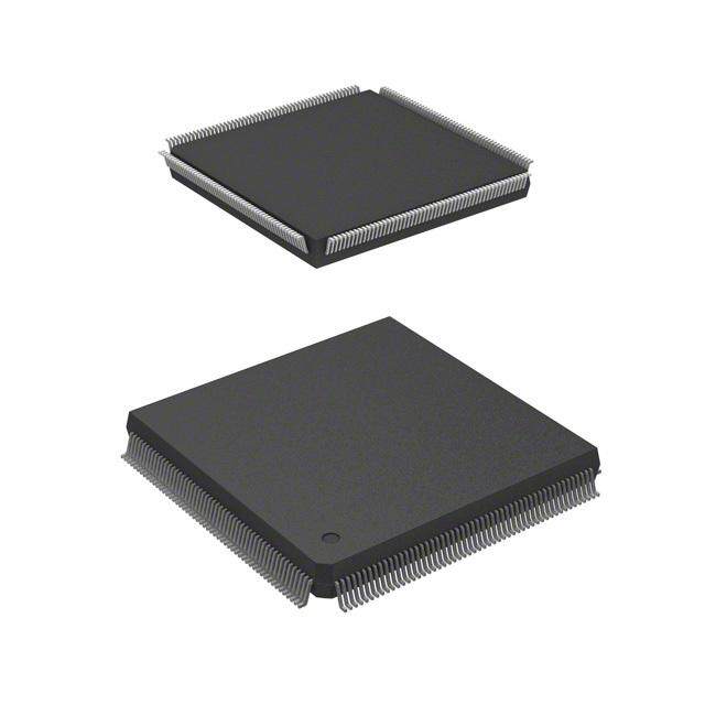
| 描述 | IC FPGA 83 I/O 100VQFP |
| 产品分类 | |
| I/O数 | 83 |
| LAB/CLB数 | - |
| 品牌 | Microsemi SoC |
| 数据手册 | http://www.microsemi.com/index.php?option=com_docman&task=doc_download&gid=130699 |
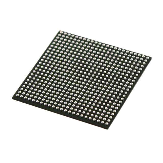
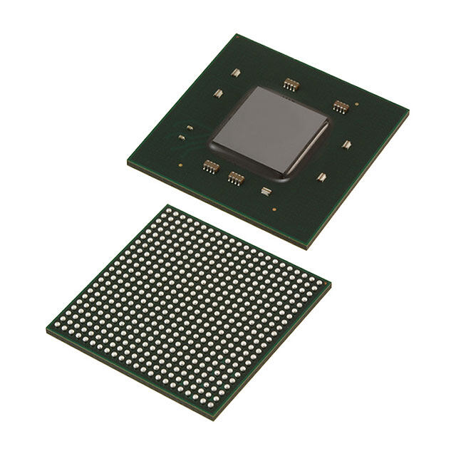
| 产品图片 |
|
| 产品型号 | A42MX09-VQG100 |
| rohs | 无铅 / 符合限制有害物质指令(RoHS)规范要求 |
| 产品系列 | MX |
| 供应商器件封装 | 100-VQFP(14x14) |
| 其它名称 | 1100-1052 |
| 安装类型 | 表面贴装 |
| 封装/外壳 | 100-TQFP |
| 工作温度 | 0°C ~ 70°C |
| 总RAM位数 | - |
| 栅极数 | 14000 |
| 标准包装 | 90 |
| 电压-电源 | 3 V ~ 3.6 V,4.75 V ~ 5.25 V |
| 逻辑元件/单元数 | - |


- 商务部:美国ITC正式对集成电路等产品启动337调查
- 曝三星4nm工艺存在良率问题 高通将骁龙8 Gen1或转产台积电
- 太阳诱电将投资9.5亿元在常州建新厂生产MLCC 预计2023年完工
- 英特尔发布欧洲新工厂建设计划 深化IDM 2.0 战略
- 台积电先进制程称霸业界 有大客户加持明年业绩稳了
- 达到5530亿美元!SIA预计今年全球半导体销售额将创下新高
- 英特尔拟将自动驾驶子公司Mobileye上市 估值或超500亿美元
- 三星加码芯片和SET,合并消费电子和移动部门,撤换高东真等 CEO
- 三星电子宣布重大人事变动 还合并消费电子和移动部门
- 海关总署:前11个月进口集成电路产品价值2.52万亿元 增长14.8%


PDF Datasheet 数据手册内容提取
Revision 11 40MX and 42MX FPGA Families Features HiRel Features • Commercial, Industrial, Automotive, and Military High Capacity Temperature Plastic Packages • Single-Chip ASIC Alternative • Commercial, Military Temperature, and MIL-STD-883 • 3,000 to 54,000 System Gates Ceramic Packages • Up to 2.5 kbits Configurable Dual-Port SRAM • QML Certification • Fast Wide-Decode Circuitry • Ceramic Devices Available to DSCC SMD • Up to 202 User-Programmable I/O Pins Ease of Integration High Performance • Mixed-Voltage Operation (5.0V or 3.3V for core and • 5.6 ns Clock-to-Out I/Os), with PCI-Compliant I/Os • 250 MHz Performance • Up to 100% Resource Utilization and 100% Pin Locking • 5 ns Dual-Port SRAM Access • Deterministic, User-Controllable Timing • 100 MHz FIFOs • Unique In-System Diagnostic and Verification Capability with Silicon Explorer II • 7.5 ns 35-Bit Address Decode • Low Power Consumption • IEEE Standard 1149.1 (JTAG) Boundary Scan Testing Product Profile Device A40MX02 A40MX04 A42MX09 A42MX16 A42MX24 A42MX36 Capacity System Gates 3,000 6,000 14,000 24,000 36,000 54,000 SRAM Bits – – – – – 2,560 Logic Modules Sequential – – 348 624 954 1,230 Combinatorial 295 547 336 608 912 1,184 Decode – – – – 24 24 Clock-to-Out 9.5 ns 9.5 ns 5.6 ns 6.1 ns 6.1 ns 6.3 ns SRAM Modules (64x4 or 32x8) – – – – – 10 Dedicated Flip-Flops – – 348 624 954 1,230 Maximum Flip-Flops 147 273 516 928 1,410 1,822 Clocks 1 1 2 2 2 6 User I/O (maximum) 57 69 104 140 176 202 PCI – – – – Yes Yes Boundary Scan Test (BST) – – – – Yes Yes Packages (by pin count) PLCC 44, 68 44, 68, 84 84 84 84 – PQFP 100 100 100, 160 100, 160, 208 160, 208 208, 240 VQFP 80 80 100 100 – – TQFP – – 176 176 176 – CQFP – – – – – 208, 256 PBGA – – – – – 272 May 2012 i © 2012 Microsemi Corporation
40MX and 42MX FPGA Families Ordering Information _ A42MX16 1 PQ G 100 ES Application (Temperature Range) Blank = Commercial (0 to +70°C) I = Industrial (–40 to +85°C) M = Military (–55 to +125°C) B = MIL-STD-883 A = Automotive (–40 to +125°C) Package Lead Count Lead-Free Packaging Blank = Standard Packaging G = RoHS Compliant Packaging Package Type PL = Plastic Leaded Chip Carrier PQ = Plastic Quad Flat Pack TQ = Thin (1.4 mm) Quad Flat Pack VQ = Very Thin (1.0 mm) Quad Flat Pack BG = Plastic Ball Grid Array CQ =Ceramic Quad Flat Pack Speed Grade Blank = Standard Speed –1 = Approximately 15% Faster than Standard –2 = Approximately 25% Faster than Standard –3 = Approximately 35% Faster than Standard –F = Approximately 40% Slower than Standard Part Number A40MX02 = 3,000 System Gates A40MX04 = 6,000 System Gates A42MX09 = 14,000 System Gates A42MX16 = 24,000 System Gates A42MX24 = 36,000 System Gates A42MX36 = 54,000 System Gates Plastic Device Resources User I/Os PLCC PLCC PLCC PQFP PQFP PQFP PQFP VQFP VQFP TQFP PBGA Device 44-Pin 68-Pin 84-Pin 100-Pin 160-Pin 208-Pin 240-Pin 80-Pin 100-Pin 176-Pin 272-Pin A40MX02 34 57 – 57 – – – 57 – – – A40MX04 34 57 69 69 – – – 69 – – – A42MX09 – – 72 83 101 – – – 83 104 – A42MX16 – – 72 83 125 140 – – 83 140 – A42MX24 – – 72 – 125 176 – – – 150 – A42MX36 – – – – – 176 202 – – – 202 Note: Package Definitions PLCC = Plastic Leaded Chip Carrier, PQFP = Plastic Quad Flat Pack, TQFP = Thin Quad Flat Pack, VQFP = Very Thin Quad Flat Pack, PBGA = Plastic Ball Grid Array ii Revision 11
40MX and 42MX FPGA Families Ceramic Device Resources User I/Os Device CQFP 208-Pin CQFP 256-Pin A42MX36 176 202 Note: Package Definitions CQFP = Ceramic Quad Flat Pack Temperature Grade Offerings Package A40MX02 A40MX04 A42MX09 A42MX16 A42MX24 A42MX36 PLCC 44 C, I, M C, I, M PLCC 68 C, I, A, M C, I, M PLCC 84 C, I, A, M C, I, A, M C, I, M C, I, M PQFP 100 C, I, A, M C, I, A, M C, I, A, M C, I, M PQFP 160 C, I, A, M C, I, M C, I, A, M PQFP 208 C, I, A, M C, I, A, M C, I, A, M PQFP 240 C, I, A, M VQFP 80 C, I, A, M C, I, A, M VQFP 100 C, I, A, M C, I, A, M TQFP 176 C, I, A, M C, I, A, M C, I, A, M PBGA 272 C, I, M CQFP 208 C, M, B CQFP 256 C, M, B Note: C = Commercial I = Industrial A = Automotive M = Military B = MIL-STD-883 Class B Speed Grade Offerings – F Std –1 –2 –3 C ✓ ✓ ✓ ✓ ✓ I ✓ ✓ ✓ ✓ A ✓ M ✓ ✓ B ✓ ✓ Note: Refer to the 40MX and 42MX Automotive Family FPGAs datasheet for details on automotive-grade MX offerings. Contact your local Microsemi SoC Products Group representative for device availability. Revision 11 iii
40MX and 42MX FPGA Families Table of Contents 40MX and 42MX FPGA Families General Description . . . . . . . . . . . . . . . . . . . . . . . . . . . . . . . . . . . . . . . . . . . . . . . . . . . . . . . . . . . . . . . . . . . . . . . . . . 1-1 MX Architectural Overview . . . . . . . . . . . . . . . . . . . . . . . . . . . . . . . . . . . . . . . . . . . . . . . . . . . . . . . . . . . . . . . . . . . . 1-1 Other Architectural Features . . . . . . . . . . . . . . . . . . . . . . . . . . . . . . . . . . . . . . . . . . . . . . . . . . . . . . . . . . . . . . . . . . . 1-8 Power Dissipation . . . . . . . . . . . . . . . . . . . . . . . . . . . . . . . . . . . . . . . . . . . . . . . . . . . . . . . . . . . . . . . . . . . . . . . . . . 1-10 Development Tool Support . . . . . . . . . . . . . . . . . . . . . . . . . . . . . . . . . . . . . . . . . . . . . . . . . . . . . . . . . . . . . . . . . . . 1-16 Related Documents . . . . . . . . . . . . . . . . . . . . . . . . . . . . . . . . . . . . . . . . . . . . . . . . . . . . . . . . . . . . . . . . . . . . . . . . . 1-16 5.0 V Operating Conditions . . . . . . . . . . . . . . . . . . . . . . . . . . . . . . . . . . . . . . . . . . . . . . . . . . . . . . . . . . . . . . . . . . . 1-16 3.3 V Operating Conditions . . . . . . . . . . . . . . . . . . . . . . . . . . . . . . . . . . . . . . . . . . . . . . . . . . . . . . . . . . . . . . . . . . . 1-19 Mixed 5.0V/3.3V Operating Conditions (for 42MX Devices Only) . . . . . . . . . . . . . . . . . . . . . . . . . . . . . . . . . . . . 1-21 Timing Models . . . . . . . . . . . . . . . . . . . . . . . . . . . . . . . . . . . . . . . . . . . . . . . . . . . . . . . . . . . . . . . . . . . . . . . . . . . . . 1-27 Timing Characteristics . . . . . . . . . . . . . . . . . . . . . . . . . . . . . . . . . . . . . . . . . . . . . . . . . . . . . . . . . . . . . . . . . . . . . . . 1-35 Pin Descriptions . . . . . . . . . . . . . . . . . . . . . . . . . . . . . . . . . . . . . . . . . . . . . . . . . . . . . . . . . . . . . . . . . . . . . . . . . . . . 1-83 Package Pin Assignments PL44 . . . . . . . . . . . . . . . . . . . . . . . . . . . . . . . . . . . . . . . . . . . . . . . . . . . . . . . . . . . . . . . . . . . . . . . . . . . . . . . . . . . . . 2-1 PL68 . . . . . . . . . . . . . . . . . . . . . . . . . . . . . . . . . . . . . . . . . . . . . . . . . . . . . . . . . . . . . . . . . . . . . . . . . . . . . . . . . . . . . 2-3 PL84 . . . . . . . . . . . . . . . . . . . . . . . . . . . . . . . . . . . . . . . . . . . . . . . . . . . . . . . . . . . . . . . . . . . . . . . . . . . . . . . . . . . . . 2-5 PQ100 . . . . . . . . . . . . . . . . . . . . . . . . . . . . . . . . . . . . . . . . . . . . . . . . . . . . . . . . . . . . . . . . . . . . . . . . . . . . . . . . . . . . 2-9 PQ160 . . . . . . . . . . . . . . . . . . . . . . . . . . . . . . . . . . . . . . . . . . . . . . . . . . . . . . . . . . . . . . . . . . . . . . . . . . . . . . . . . . . 2-13 PQ208 . . . . . . . . . . . . . . . . . . . . . . . . . . . . . . . . . . . . . . . . . . . . . . . . . . . . . . . . . . . . . . . . . . . . . . . . . . . . . . . . . . . 2-19 PQ240 . . . . . . . . . . . . . . . . . . . . . . . . . . . . . . . . . . . . . . . . . . . . . . . . . . . . . . . . . . . . . . . . . . . . . . . . . . . . . . . . . . . 2-26 VQ80 . . . . . . . . . . . . . . . . . . . . . . . . . . . . . . . . . . . . . . . . . . . . . . . . . . . . . . . . . . . . . . . . . . . . . . . . . . . . . . . . . . . . 2-30 VQ100 . . . . . . . . . . . . . . . . . . . . . . . . . . . . . . . . . . . . . . . . . . . . . . . . . . . . . . . . . . . . . . . . . . . . . . . . . . . . . . . . . . . 2-32 TQ176 . . . . . . . . . . . . . . . . . . . . . . . . . . . . . . . . . . . . . . . . . . . . . . . . . . . . . . . . . . . . . . . . . . . . . . . . . . . . . . . . . . . 2-34 CQ208 . . . . . . . . . . . . . . . . . . . . . . . . . . . . . . . . . . . . . . . . . . . . . . . . . . . . . . . . . . . . . . . . . . . . . . . . . . . . . . . . . . . 2-40 CQ256 . . . . . . . . . . . . . . . . . . . . . . . . . . . . . . . . . . . . . . . . . . . . . . . . . . . . . . . . . . . . . . . . . . . . . . . . . . . . . . . . . . . 2-43 BG272 . . . . . . . . . . . . . . . . . . . . . . . . . . . . . . . . . . . . . . . . . . . . . . . . . . . . . . . . . . . . . . . . . . . . . . . . . . . . . . . . . . . 2-47 Datasheet Information List of Changes . . . . . . . . . . . . . . . . . . . . . . . . . . . . . . . . . . . . . . . . . . . . . . . . . . . . . . . . . . . . . . . . . . . . . . . . . . . . . 3-1 Datasheet Categories . . . . . . . . . . . . . . . . . . . . . . . . . . . . . . . . . . . . . . . . . . . . . . . . . . . . . . . . . . . . . . . . . . . . . . . . 3-3 Revision 11 iv
1 – 40MX and 42MX FPGA Families General Description Microsemi's 40MX and 42MX families offer a cost-effective design solution at 5V. The MX devices are single-chip solutions and provide high performance while shortening the system design and development cycle. MX devices can integrate and consolidate logic implemented in multiple PALs, CPLDs, and FPGAs. Example applications include high-speed controllers and address decoding, peripheral bus interfaces, DSP, and co-processor functions. The MX device architecture is based on Microsemi’s patented antifuse technology implemented in a 0.45µm triple-metal CMOS process. With capacities ranging from 3,000 to 54,000 system gates, the MX devices provide performance up to 250MHz, are live on power-up and have one-fifth the standby power consumption of comparable FPGAs. MX FPGAs provide up to 202 user I/Os and are available in a wide variety of packages and speed grades. A42MX24 and A42MX36 devices also feature MultiPlex I/Os, which support mixed-voltage systems, enable programmable PCI, deliver high-performance operation at both 5.0V and 3.3V, and provide a low- power mode. The devices are fully compliant with the PCI Local Bus Specification (version 2.1). They deliver 200MHz on-chip operation and 6.1ns clock-to-output performance. The 42MX24 and 42MX36 devices include system-level features such as IEEE Standard 1149.1 (JTAG) Boundary Scan Testing and fast wide-decode modules. In addition, the A42MX36 device offers dual-port SRAM for implementing fast FIFOs, LIFOs, and temporary data storage. The storage elements can efficiently address applications requiring wide datapath manipulation and can perform transformation functions such as those required for telecommunications, networking, and DSP. All MX devices are fully tested over automotive and military temperature ranges. In addition, the largest member of the family, the A42MX36, is available in both CQ208 and CQ256 ceramic packages screened to MIL-STD-883 levels. For easy prototyping and conversion from plastic to ceramic, the CQ208 and PQ208 devices are pin-compatible. MX Architectural Overview The MX devices are composed of fine-grained building blocks that enable fast, efficient logic designs. All devices within these families are composed of logic modules, I/O modules, routing resources and clock networks, which are the building blocks for fast logic designs. In addition, the A42MX36 device contains embedded dual-port SRAM modules, which are optimized for high-speed datapath functions such as FIFOs, LIFOs and scratchpad memory. A42MX24 and A42MX36 also contain wide-decode modules. Logic Modules The 40MX logic module is an eight-input, one-output logic circuit designed to implement a wide range of logic functions with efficient use of interconnect routing resources (Figure1-1 on page1-2). The logic module can implement the four basic logic functions (NAND, AND, OR and NOR) in gates of two, three, or four inputs. The logic module can also implement a variety of D-latches, exclusivity functions, AND-ORs and OR-ANDs. No dedicated hard-wired latches or flip-flops are required in the array; latches and flip-flops can be constructed from logic modules whenever required in the application. Revision 11 1-1
40MX and 42MX FPGA Families Figure 1-1 • 40MX Logic Module The 42MX devices contain three types of logic modules: combinatorial (C-modules), sequential (S- modules) and decode (D-modules). Figure1-2 illustrates the combinatorial logic module. The S-module, shown in Figure1-3, implements the same combinatorial logic function as the C-module while adding a sequential element. The sequential element can be configured as either a D-flip-flop or a transparent latch. The S-module register can be bypassed so that it implements purely combinatorial logic. A0 B0 S0 D00 D01 Y D10 D11 S1 A1 B1 Figure 1-2 • 42MX C-Module Implementation 1-2 Revision 11
40MX and 42MX FPGA Families D00 D00 D01 D01 Y D Q OUT Y D Q OUT D10 D10 D11 S0 D11 S0 GATE CLR S1 S1 Up to 7-Input Function Plus D-Type Flip-Flop with Clear Up to 7-Input Function Plus Latch D00 D0 D01 Y OUT Y D Q OUT D10 D1 GATE D11 S0 S CLR S1 Up to 8-Input Function (Same as C-Module) Up to 4-Input Function Plus Latch with Clear Figure 1-3 • 42MX S-Module Implementation A42MX24 and A42MX36 devices contain D-modules, which are arranged around the periphery of the device. D-modules contain wide-decode circuitry, providing a fast, wide-input AND function similar to that found in CPLD architectures (Figure1-4). The D-module allows A42MX24 and A42MX36 devices to perform wide-decode functions at speeds comparable to CPLDs and PALs. The output of the D-module has a programmable inverter for active HIGH or LOW assertion. The D-module output is hardwired to an output pin, and can also be fed back into the array to be incorporated into other logic. Dual-Port SRAM Modules The A42MX36 device contains dual-port SRAM modules that have been optimized for synchronous or asynchronous applications. The SRAM modules are arranged in 256-bit blocks that can be configured as 32x8 or 64x4. SRAM modules can be cascaded together to form memory spaces of user-definable width and depth. A block diagram of the A42MX36 dual-port SRAM block is shown in Figure1-5. The A42MX36 SRAM modules are true dual-port structures containing independent read and write ports. Each SRAM module contains six bits of read and write addressing (RDAD[5:0] and WRAD[5:0], respectively) for 64x4-bit blocks. When configured in byte mode, the highest order address bits (RDAD5 and WRAD5) are not used. The read and write ports of the SRAM block contain independent clocks (RCLK and WCLK) with programmable polarities offering active HIGH or LOW implementation. The SRAM block contains eight data inputs (WD[7:0]), and eight outputs (RD[7:0]), which are connected to segmented vertical routing tracks. The A42MX36 dual-port SRAM blocks provide an optimal solution for high-speed buffered applications requiring FIFO and LIFO queues. The ACTgen Macro Builder within Microsemi's Designer software Revision 11 1-3
40MX and 42MX FPGA Families provides capability to quickly design memory functions with the SRAM blocks. Unused SRAM blocks can be used to implement registers for other user logic within the design. 7 Inputs Hard-Wire to I/O Programmable Inverter Feedback to Array Figure 1-4 • A42MX24 and A42MX36 D-Module Implementation WD[7:0] Latches [7:0] [5:0] RDAD[5:0] Write SRAM Module Read Latches Port 32 x 8 or 64 x 4 Port Logic (256 Bits) Logic [5:0] WRAD[5:0] Latches Read Logic REN MODE RD[7:0] RCLK BLKEN Write Logic WEN Routing Tracks WCLK Figure 1-5 • A42MX36 Dual-Port SRAM Block Routing Structure The MX architecture uses vertical and horizontal routing tracks to interconnect the various logic and I/O modules. These routing tracks are metal interconnects that may be continuous or split into segments. Varying segment lengths allow the interconnect of over 90% of design tracks to occur with only two antifuse connections. Segments can be joined together at the ends using antifuses to increase their lengths up to the full length of the track. All interconnects can be accomplished with a maximum of four antifuses. Horizontal Routing Horizontal routing tracks span the whole row length or are divided into multiple segments and are located in between the rows of modules. Any segment that spans more than one-third of the row length is considered a long horizontal segment. A typical channel is shown in Figure1-6. Within horizontal routing, dedicated routing tracks are used for global clock networks and for power and ground tie-off tracks. Non- dedicated tracks are used for signal nets. Vertical Routing Another set of routing tracks run vertically through the module. There are three types of vertical tracks: input, output, and long. Long tracks span the column length of the module, and can be divided into multiple segments. Each segment in an input track is dedicated to the input of a particular module; each segment in an output track is dedicated to the output of a particular module. Long segments are 1-4 Revision 11
40MX and 42MX FPGA Families uncommitted and can be assigned during routing. Each output segment spans four channels (two above and two below), except near the top and bottom of the array, where edge effects occur. Long vertical tracks contain either one or two segments. An example of vertical routing tracks and segments is shown in Figure1-6. Antifuse Structures An antifuse is a "normally open" structure. The use of antifuses to implement a programmable logic device results in highly testable structures as well as efficient programming algorithms. There are no pre- existing connections; temporary connections can be made using pass transistors. These temporary connections can isolate individual antifuses to be programmed and individual circuit structures to be tested, which can be done before and after programming. For instance, all metal tracks can be tested for continuity and shorts between adjacent tracks, and the functionality of all logic modules can be verified. Segmented Horizontal Logic Routing Modules Antifuses Vertical Routing Tracks Figure 1-6 • MX Routing Structure Clock Networks The 40MX devices have one global clock distribution network (CLK). A signal can be put on the CLK network by being routed through the CLKBUF buffer. In 42MX devices, there are two low-skew, high-fanout clock distribution networks, referred to as CLKA and CLKB. Each network has a clock module (CLKMOD) that can select the source of the clock signal from any of the following (Figure1-7 on page1-6): • Externally from the CLKA pad, using CLKBUF buffer • Externally from the CLKB pad, using CLKBUF buffer • Internally from the CLKINTA input, using CLKINT buffer • Internally from the CLKINTB input, using CLKINT buffer The clock modules are located in the top row of I/O modules. Clock drivers and a dedicated horizontal clock track are located in each horizontal routing channel. Clock input pads in both 40MX and 42MX devices can also be used as normal I/Os, bypassing the clock networks. The A42MX36 device has four additional register control resources, called quadrant clock networks (Figure1-8 on page1-6). Each quadrant clock provides a local, high-fanout resource to the contiguous logic modules within its quadrant of the device. Quadrant clock signals can originate from specific I/O Revision 11 1-5
40MX and 42MX FPGA Families pins or from the internal array and can be used as a secondary register clock, register clear, or output enable. CLKB CLKINB CLKA CLKINA From Pads S0 Internal CLKMOD S1 Signal CLKO(17) Clock Drivers CLKO(16) CLKO(15) CLKO(2) CLKO(1) Clock Tracks Figure 1-7 • Clock Networks of 42MX Devices QCLKA QCLKC Quad Quad QCLKB Clock QCLK1 QCLK3 Clock QCLKD Modul Modul *QCLK1IN *QCLK3IN S0 S1 S1 S0 Quad Quad Clock QCLK2 QCLK4 Clock Modul Modul *QCLK2IN *QCLK4IN S0 S1 S1 S0 Note: *QCLK1IN, QCLK2IN, QCLK3IN, and QCLK4IN are internally-generated signals. Figure 1-8 • Quadrant Clock Network of A42MX36 Devices 1-6 Revision 11
40MX and 42MX FPGA Families MultiPlex I/O Modules 42MX devices feature Multiplex I/Os and support 5.0V, 3.3V, and mixed 3.3V/5.0V operations. The MultiPlex I/O modules provide the interface between the device pins and the logic array. Figure1-9 is a block diagram of the 42MX I/O module. A variety of user functions, determined by a library macro selection, can be implemented in the module. (Refer to the Antifuse Macro Library Guide for more information.) All 42MX I/O modules contain tristate buffers, with input and output latches that can be configured for input, output, or bidirectional operation. All 42MX devices contain flexible I/O structures, where each output pin has a dedicated output-enable control (Figure1-9). The I/O module can be used to latch input or output data, or both, providing fast set- up time. In addition, the Designer software tools can build a D-type flip-flop using a C-module combined with an I/O module to register input and output signals. Refer to the Antifuse Macro Library Guide for more details. A42MX24 and A42MX36 devices also offer selectable PCI output drives, enabling 100% compliance with version 2.1 of the PCI specification. For low-power systems, all inputs and outputs are turned off to reduce current consumption to below 500μA. To achieve 5.0V or 3.3V PCI-compliant output drives on A42MX24 and A42MX36 devices, a chip-wide PCI fuse is programmed via the Device Selection Wizard in the Designer software (Figure1-10). When the PCI fuse is not programmed, the output drive is standard. Designer software development tools provide a design library of I/O macro functions that can implement all I/O configurations supported by the MX FPGAs. EN Q D PAD From Array G/CLK* To Array Q D G/CLK* Note: *Can be configured as a Latch or D Flip-Flop (Using C-Module) Figure 1-9 • 42MX I/O Module STD Signal Output PCI Drive PCI Enable Fuse Figure 1-10 • PCI Output Structure of A42MX24 and A42MX36 Devices Revision 11 1-7
40MX and 42MX FPGA Families Other Architectural Features Performance MX devices can operate with internal clock frequencies of 250 MHz, enabling fast execution of complex logic functions. MX devices are live on power-up and do not require auxiliary configuration devices and thus are an optimal platform to integrate the functionality contained in multiple programmable logic devices. In addition, designs that previously would have required a gate array to meet performance can be integrated into an MX device with improvements in cost and time-to-market. Using timing-driven place-and-route (TDPR) tools, designers can achieve highly deterministic device performance. User Security Microsemi FuseLock provides robust security against design theft. Special security fuses are hidden in the fabric of the device and protect against unauthorized users attempting to access the programming and/or probe interfaces. It is virtually impossible to identify or bypass these fuses without damaging the device, making Microsemi antifuse FPGAs protected with the highest level of security available from both invasive and noninvasive attacks. Special security fuses in 40MX devices include the Probe Fuse and Program Fuse. The former disables the probing circuitry while the latter prohibits further programming of all fuses, including the Probe Fuse. In 42MX devices, there is the Security Fuse which, when programmed, both disables the probing circuitry and prohibits further programming of the device. Programming Device programming is supported through the Silicon Sculptor series of programmers. Silicon Sculptor II is a compact, robust, single-site and multi-site device programmer for the PC. With standalone software, Silicon Sculptor II is designed to allow concurrent programming of multiple units from the same PC. Silicon Sculptor II programs devices independently to achieve the fastest programming times possible. After being programmed, each fuse is verified to insure that it has been programmed correctly. Furthermore, at the end of programming, there are integrity tests that are run to ensure no extra fuses have been programmed. Not only does it test fuses (both programmed and nonprogrammed), Silicon Sculptor II also allows self-test to verify its own hardware extensively. The procedure for programming an MX device using Silicon Sculptor II is as follows: 1. Load the *.AFM file 2. Select the device to be programmed 3. Begin programming When the design is ready to go to production, Microsemi offers device volume-programming services either through distribution partners or via In-House Programming from the factory. For more details on programming MX devices, please refer to the Programming Antifuse Devices and the Silicon Sculptor II user's guides. 1-8 Revision 11
40MX and 42MX FPGA Families Power Supply MX devices are designed to operate in both 5.0V and 3.3V environments. In particular, 42MX devices can operate in mixed 5.0V/3.3V systems. Table1-1 describes the voltage support of MX devices. Table1-1 • Voltage Support of MX Devices Device VCC VCCA VCCI Maximum Input Tolerance Nominal Output Voltage 40MX 5.0 V – – 5.5 V 5.0V 3.3 V – – 3.6 V 3.3V 42MX – 5.0 V 5.0 V 5.5 V 5.0V – 3.3 V 3.3 V 3.6 V 3.3V – 5.0 V 3.3 V 5.5 V 3.3V Power-Up/Down in Mixed-Voltage Mode When powering up 42MX in mixed voltage mode (VCCA=5.0 V and VCCI = 3.3 V), VCCA must be greater than or equal to VCCI throughout the power-up sequence. If VCCI exceeds VCCA during power- up, one of two things will happen: • The input protection diode on the I/Os will be forward biased • The I/Os will be at logical High In either case, ICC rises to high levels. For power-down, any sequence with VCCA and VCCI can be implemented. Transient Current Due to the simultaneous random logic switching activity during power-up, a transient current may appear on the core supply (VCC). Customers must use a regulator for the VCC supply that can source a minimum of 100mA for transient current during power-up. Failure to provide enough power can prevent the system from powering up properly and result in functional failure. However, there are no reliability concerns, since transient current is distributed across the die instead of confined to a localized spot. Since the transient current is not due to I/O switching, its value and duration are independent of the VCCI. Low Power Mode 42MX devices have been designed with a Low Power Mode. This feature, activated with setting the special LP pin to HIGH for a period longer than 800 ns, is particularly useful for battery-operated systems where battery life is a primary concern. In this mode, the core of the device is turned off and the device consumes minimal power with low standby current. In addition, all input buffers are turned off, and all outputs and bidirectional buffers are tristated. Since the core of the device is turned off, the states of the registers are lost. The device must be re-initialized when exiting Low Power Mode. I/Os can be driven during LP mode, and clock pins should be driven HIGH or LOW and should not float to avoid drawing current. To exit LP mode, the LP pin must be pulled LOW for over 200 µs to allow for charge pumps to power up, and device initialization will begin. Revision 11 1-9
40MX and 42MX FPGA Families Power Dissipation The general power consumption of MX devices is made up of static and dynamic power and can be expressed with the following equation: General Power Equation P = [ICCstandby + ICCactive] * VCCI + IOL* VOL* N + IOH * (VCCI – VOH) * M where: ICCstandby is the current flowing when no inputs or outputs are changing. ICCactive is the current flowing due to CMOS switching. IOL, IOH are TTL sink/source currents. VOL, VOH are TTL level output voltages. N equals the number of outputs driving TTL loads to VOL. M equals the number of outputs driving TTL loads to VOH. Accurate values for N and M are difficult to determine because they depend on the family type, on design details, and on the system I/O. The power can be divided into two components: static and active. Static Power Component The static power due to standby current is typically a small component of the overall power consumption. Standby power is calculated for commercial, worst-case conditions. The static power dissipation by TTL loads depends on the number of outputs driving, and on the DC load current. For instance, a 32-bit bus sinking 4mA at 0.33V will generate 42mW with all outputs driving LOW, and 140mW with all outputs driving HIGH. The actual dissipation will average somewhere in between, as I/Os switch states with time. Active Power Component Power dissipation in CMOS devices is usually dominated by the dynamic power dissipation. Dynamic power consumption is frequency-dependent and is a function of the logic and the external I/O. Active power dissipation results from charging internal chip capacitances of the interconnect, unprogrammed antifuses, module inputs, and module outputs, plus external capacitances due to PC board traces and load device inputs. An additional component of the active power dissipation is the totem pole current in the CMOS transistor pairs. The net effect can be associated with an equivalent capacitance that can be combined with frequency and voltage to represent active power dissipation. The power dissipated by a CMOS circuit can be expressed by the equation: Power (µW) = C * VCCA2 * F(1) EQ where: C = Equivalent capacitance expressed in picofarads (pF) EQ VCCA = Power supply in volts (V) F = Switching frequency in megahertz (MHz) Equivalent Capacitance Equivalent capacitance is calculated by measuring ICCactive at a specified frequency and voltage for each circuit component of interest. Measurements have been made over a range of frequencies at a fixed value of VCC. Equivalent capacitance is frequency-independent, so the results can be used over a wide range of operating conditions. Equivalent capacitance values are shown below. 1-10 Revision 11
40MX and 42MX FPGA Families C Values for Microsemi MX FPGAs EQ Modules (C )3.5 EQM Input Buffers (C )6.9 EQI Output Buffers (C )18.2 EQO Routed Array Clock Buffer Loads (C )1.4 EQCR To calculate the active power dissipated from the complete design, the switching frequency of each part of the logic must be known. The equation below shows a piece-wise linear summation over all components. Power = VCCA2 * [(m x C * f ) + EQM m Modules (n * C * f ) + (p * (C + C ) * f ) + EQI n Inputs EQO L p outputs 0.5 * (q * C * f ) + (r * f ) + 1 EQCR q1routed_Clk1 1 q1 routed_Clk1 0.5 * (q * C * f ) + (r * f ) (2) 2 EQCR q2routed_Clk2 2 q2 routed_Clk2 where: m = Number of logic modules switching at frequency f m n = Number of input buffers switching at frequency f n p = Number of output buffers switching at frequency f p q = Number of clock loads on the first routed array clock 1 q = Number of clock loads on the second routed array clock 2 r = Fixed capacitance due to first routed array clock 1 r = Fixed capacitance due to second routed array clock 2 C = Equivalent capacitance of logic modules in pF EQM C = Equivalent capacitance of input buffers in pF EQI C = Equivalent capacitance of output buffers in pF EQO C = Equivalent capacitance of routed array clock in pF EQC R C = Output load capacitance in pF L f = Average logic module switching rate in MHz m f = Average input buffer switching rate in MHz n f = Average output buffer switching rate in MHz p f = Average first routed array clock rate in MHz q1 f = Average second routed array clock rate in MHz q2 Fixed Capacitance Values for MX FPGAs (pF) r1 r2 Device Type routed_Clk1 routed_Clk2 A40MX02 41.4 N/A A40MX04 68.6 N/A A42MX09 118 118 A42MX16 165 165 A42MX24 185 185 A42MX36 220 220 Revision 11 1-11
40MX and 42MX FPGA Families Test Circuitry and Silicon Explorer II Probe MX devices contain probing circuitry that provides built-in access to every node in a design, via the use of Silicon Explorer II. Silicon Explorer II is an integrated hardware and software solution that, in conjunction with the Designer software, allow users to examine any of the internal nets of the device while it is operating in a prototyping or a production system. The user can probe into an MX device without changing the placement and routing of the design and without using any additional resources. Silicon ExplorerII's noninvasive method does not alter timing or loading effects, thus shortening the debug cycle and providing a true representation of the device under actual functional situations. Silicon Explorer II samples data at 100 MHz (asynchronous) or 66 MHz (synchronous). Silicon Explorer II attaches to a PC's standard COM port, turning the PC into a fully functional 18-channel logic analyzer. Silicon Explorer II allows designers to complete the design verification process at their desks and reduces verification time from several hours per cycle to a few seconds. Silicon Explorer II is used to control the MODE, DCLK, SDI and SDO pins in MX devices to select the desired nets for debugging. The user simply assigns the selected internal nets in the Silicon Explorer II software to the PRA/PRB output pins for observation. Probing functionality is activated when the MODE pin is held HIGH. Figure1-11 illustrates the interconnection between Silicon Explorer II and 40MX devices, while Figure1- 12 on page1-12 illustrates the interconnection between Silicon Explorer II and 42MX devices To allow for probing capabilities, the security fuses must not be programmed. (Refer to "User Security" section on page1-8 for the security fuses of 40MX and 42MX devices). Table1-2 on page1-13 summarizes the possible device configurations for probing. PRA and PRB pins are dual-purpose pins. When the "Reserve Probe Pin" is checked in the Designer software, PRA and PRB pins are reserved as dedicated outputs for probing. If PRA and PRB pins are required as user I/Os to achieve successful layout and "Reserve Probe Pin" is checked, the layout tool will override the option and place user I/Os on PRA and PRB pins. 16 Logic Analyzer Channels 40MX Serial Connection to Windows PC MODE Silicon SDI Explorer II DCLK SDO PRA PRB Figure 1-11 • Silicon Explorer II Setup with 40MX 16 Logic Analyzer Channels 42MX Serial Connection to Windows PC MODE Silicon SDI Explorer II DCLK SDO PRA PRB Figure 1-12 • Silicon Explorer II Setup with 42MX 1-12 Revision 11
40MX and 42MX FPGA Families Table1-2 • Device Configuration Options for Probe Capability Security Fuse(s) Programmed Mode PRA, PRB1 SDI, SDO, DCLK1 No LOW User I/Os2 User I/Os2 No HIGH Probe Circuit Outputs Probe Circuit Inputs Yes – Probe Circuit Secured Probe Circuit Secured Notes: 1. Avoid using SDI, SDO, DCLK, PRA and PRB pins as input or bidirectional ports. Since these pins are active during probing, input signals will not pass through these pins and may cause contention. 2. If no user signal is assigned to these pins, they will behave as unused I/Os in this mode. See the "Pin Descriptions" section on page1-83 for information on unused I/O pins. Design Consideration It is recommended to use a series 70Ω termination resistor on every probe connector (SDI, SDO, MODE, DCLK, PRA and PRB). The 70Ω series termination is used to prevent data transmission corruption during probing and reading back the checksum. IEEE Standard 1149.1 Boundary Scan Test (BST) Circuitry 42MX24 and 42MX36 devices are compatible with IEEE Standard 1149.1 (informally known as Joint Testing Action Group Standard or JTAG), which defines a set of hardware architecture and mechanisms for cost-effective board-level testing. The basic MX boundary-scan logic circuit is composed of the TAP (test access port), TAP controller, test data registers and instruction register (Figure1-13 on page1-14). This circuit supports all mandatory IEEE 1149.1 instructions (EXTEST, SAMPLE/PRELOAD and BYPASS) and some optional instructions. Table1-3 on page1-14 describes the ports that control JTAG testing, while Table1-4 on page1-14 describes the test instructions supported by these MX devices. Each test section is accessed through the TAP, which has four associated pins: TCK (test clock input), TDI and TDO (test data input and output), and TMS (test mode selector). The TAP controller is a four-bit state machine. The '1's and '0's represent the values that must be present at TMS at a rising edge of TCK for the given state transition to occur. IR and DR indicate that the instruction register or the data register is operating in that state. The TAP controller receives two control inputs (TMS and TCK) and generates control and clock signals for the rest of the test logic architecture. On power-up, the TAP controller enters the Test-Logic-Reset state. To guarantee a reset of the controller from any of the possible states, TMS must remain high for five TCK cycles. 42MX24 and 42MX36 devices support three types of test data registers: bypass, device identification, and boundary scan. The bypass register is selected when no other register needs to be accessed in a device. This speeds up test data transfer to other devices in a test data path. The 32-bit device identification register is a shift register with four fields (lowest significant byte (LSB), ID number, part number and version). The boundary-scan register observes and controls the state of each I/O pin. Each I/O cell has three boundary-scan register cells, each with a serial-in, serial-out, parallel-in, and parallel-out pin. The serial pins are used to serially connect all the boundary-scan register cells in a device into a boundary-scan register chain, which starts at the TDI pin and ends at the TDO pin. The Revision 11 1-13
40MX and 42MX FPGA Families parallel ports are connected to the internal core logic tile and the input, output and control ports of an I/O buffer to capture and load data into the register to control or observe the logic state of each I/O. Boundary Scan Register Output TDO MUX Bypass Register Control Logic JTAG TMS Instruction TAP Controller Decode TCK JTAG Instruction TDI Register Figure 1-13 • 42MX IEEE 1149.1 Boundary Scan Circuitry Table1-3 • Test Access Port Descriptions Port Description TMS Serial input for the test logic control bits. Data is captured on the rising edge of the test logic (Test Mode Select) clock (TCK). TCK Dedicated test logic clock used serially to shift test instruction, test data, and control inputs (Test Clock Input) on the rising edge of the clock, and serially to shift the output data on the falling edge of the clock. The maximum clock frequency for TCK is 20 MHz. TDI Serial input for instruction and test data. Data is captured on the rising edge of the test logic (Test Data Input) clock. TDO Serial output for test instruction and data from the test logic. TDO is set to an Inactive Drive (Test Data Output) state (high impedance) when data scanning is not in progress. Table1-4 • Supported BST Public Instructions IR Code Instruction Instruction (IR2.IR0) Type Description EXTEST 000 Mandatory Allows the external circuitry and board-level interconnections to be tested by forcing a test pattern at the output pins and capturing test results at the input pins. SAMPLE/PRELOAD 001 Mandatory Allows a snapshot of the signals at the device pins to be captured and examined during operation HIGH Z 101 Optional Tristates all I/Os to allow external signals to drive pins. Please refer to the IEEE Standard 1149.1 specification. CLAMP 110 Optional Allows state of signals driven from component pins to be determined from the Boundary-Scan Register. Please refer to the IEEE Standard 1149.1 specification for details. BYPASS 111 Mandatory Enables the bypass register between the TDI and TDO pins. The test data passes through the selected device to adjacent devices in the test chain. 1-14 Revision 11
40MX and 42MX FPGA Families JTAG Mode Activation The JTAG test logic circuit is activated in the Designer software by selecting Tools -> Device Selection. This brings up the Device Selection dialog box as shown in Figure1-14. The JTAG test logic circuit can be enabled by clicking the "Reserve JTAG Pins" check box. Table1-5 explains the pins' behavior in either mode. Figure 1-14 • Device Selection Wizard Table1-5 • Boundary Scan Pin Configuration and Functionality Reserve JTAG Checked Unchecked TCK BST input; must be terminated to logical HIGH or LOW to avoid floating User I/O TDI, TMS BST input; may float or be tied to HIGH User I/O TDO BST output; may float or be connected to TDI of another device User I/O TRST Pin and TAP Controller Reset An active reset (TRST) pin is not supported; however, MX devices contain power-on circuitry that resets the boundary scan circuitry upon power-up. Also, the TMS pin is equipped with an internal pull-up resistor. This allows the TAP controller to remain in or return to the Test-Logic-Reset state when there is no input or when a logical 1 is on the TMS pin. To reset the controller, TMS must be HIGH for at least five TCK cycles. Boundary Scan Description Language (BSDL) File Conforming to the IEEE Standard 1149.1 requires that the operation of the various JTAG components be documented. The BSDL file provides the standard format to describe the JTAG components that can be used by automatic test equipment software. The file includes the instructions that are supported, instruction bit pattern, and the boundary-scan chain order. For an in-depth discussion on BSDL files, please refer to Actel BSDL Files Format Description application note. BSDL files are grouped into two categories - generic and device-specific. The generic files assign all user I/Os as inouts. Device-specific files assign user I/Os as inputs, outputs or inouts. Generic files for MX devices are available on the Microsemi SoC Product Group's website: http://www.microsemi.com/soc/techdocs/models/bsdl.html. Revision 11 1-15
40MX and 42MX FPGA Families Development Tool Support The MX family of FPGAs is fully supported by Libero® Integrated Design Environment (IDE). Libero IDE is a design management environment, seamlessly integrating design tools while guiding the user through the design flow, managing all design and log files, and passing necessary design data among tools. Libero IDE allows users to integrate both schematic and HDL synthesis into a single flow and verify the entire design in a single environment. Libero IDE includes SynplifyPro from Synopsys, ModelSim® HDL Simulator from Mentor Graphics,® and Viewdraw. Libero IDE includes place-and-route and provides a comprehensive suite of backend support tools for FPGA development, including timing-driven place-and-route, and a world-class integrated static timing analyzer and constraints editor. Additionally, the back-annotation flow is compatible with all the major simulators and the simulation results can be cross-probed with Silicon Explorer II, Microsemi’s integrated verification and logic analysis tool. Another tool included in the Libero software is the SmartGen macro builder, which easily creates popular and commonly used logic functions for implementation into your schematic or HDL design. Microsemi’s Libero software is compatible with the most popular FPGA design entry and verification tools from companies such as Mentor Graphics, Synopsys, and Cadence Design Systems. Refer to the Libero IDE web content at www.microsemi.com/soc/products/software/libero/default.aspx for further information on licensing and current operating system support. Related Documents Application Notes Actel BSDL Files Format Description www.microsemi.com/soc/documents/BSDLformat_AN.pdf Programming Antifuse Devices http://www.microsemi.com/soc/documents/AntifuseProgram_AN.pdf Actel's Implementation of Security in Actel Antifuse FPGAs www.microsemi.com/documents/Antifuse_Security_AN.pdf User’s Guides and Manuals Antifuse Macro Library Guide www.microsemicom/soc/documents/libguide_UG.pdf Silicon Sculptor II www.microsemi.com/soc/techdocs/manuals/default.asp#programmers Miscellaneous Libero IDE Flow Diagram www.microsemi.com/soc/products/tools/libero/flow.html 5.0 V Operating Conditions Table1-6 • Absolute Maximum Ratings for 40MX Devices* Symbol Parameter Limits Units VCC DC Supply Voltage –0.5 to +7.0 V VI Input Voltage –0.5 to VCC+0.5 V VO Output Voltage –0.5 to VCC+0.5 V 1-16 Revision 11
40MX and 42MX FPGA Families Table1-6 • Absolute Maximum Ratings for 40MX Devices* Symbol Parameter Limits Units t Storage Temperature –65 to +150 °C STG Note: *Stresses beyond those listed under "Absolute Maximum Ratings" may cause permanent damage to the device. Exposure to absolute maximum rated conditions for extended periods may affect device reliability. Devices should not be operated outside the Recommended Operating Conditions. Table1-7 • Absolute Maximum Ratings for 42MX Devices* Symbol Parameter Limits Units VCCI DC Supply Voltage for I/Os –0.5 to +7.0 V VCCA DC Supply Voltage for Array –0.5 to +7.0 V VI Input Voltage –0.5 to VCCI+0.5 V VO Output Voltage –0.5 to VCCI+0.5 V t Storage Temperature –65 to +150 °C STG Note: *Stresses beyond those listed under "Absolute Maximum Ratings" may cause permanent damage to the device. Exposure to absolute maximum rated conditions for extended periods may affect device reliability. Devices should not be operated outside the Recommended Operating Conditions. Table1-8 • Recommended Operating Conditions Parameter Commercial Industrial Military Units Temperature Range* 0 to +70 –40 to +85 –55 to +125 °C VCC (40MX) 4.75 to 5.25 4.5 to 5.5 4.5 to 5.5 V VCCA (42MX) 4.75 to 5.25 4.5 to 5.5 4.5 to 5.5 V VCCI (42MX) 4.75 to 5.25 4.5 to 5.5 4.5 to 5.5 V Note: *Ambient temperature (T ) is used for commercial and industrial grades; case temperature (T ) is used for A C military grades. Revision 11 1-17
40MX and 42MX FPGA Families 5 V TTL Electrical Specifications Table1-9 • 5V TTL Electrical Specifications Commercial Commercial -F Industrial Military Symbol Parameter Min. Max. Min. Max. Min. Max. Min. Max. Units VOH1 IOH = –10 mA 2.4 2.4 V IOH = –4 mA 3.7 3.7 V VOL1 IOL = 10 mA 0.5 0.5 V IOL = 6 mA 0.4 0.4 V VIL –0.3 0.8 –0.3 0.8 –0.3 0.8 –0.3 0.8 V VIH (40MX) 2.0 VCC + 0.3 2.0 VCC + 0.3 2.0 VCC + 0.3 2.0 VCC + 0.3 V VIH (42MX) 2.0 VCCI + 0.3 2.0 VCCI + 0.3 2.0 VCCI + 0.3 2.0 VCCI + 0.3 V IIL VIN = 0.5 V –10 –10 –10 –10 µA IIH VIN = 2.7 V –10 –10 –10 –10 µA Input Transition 500 500 500 500 ns Time, T and T R F C I/O 10 10 10 10 pF IO Capacitance Standby Current,A40MX02, 3 25 10 25 mA ICC2 A40MX04 A42MX09 5 25 25 25 mA A42MX16 6 25 25 25 mA A42MX24, 20 25 25 25 mA A42MX36 Low power mode42MX devices 0.5 ICC – 5.0 ICC – 5.0 ICC – 5.0 mA Standby Current only IIO,I/O source Can be derived from the IBIS model (http://www.microsemi.com/soc/techdocs/models/ibis.html) sink current Notes: 1. Only one output tested at a time. VCC/VCCI = min. 2. All outputs unloaded. All inputs = VCC/VCCI or GND. 1-18 Revision 11
40MX and 42MX FPGA Families 3.3 V Operating Conditions Table1-10 • Absolute Maximum Ratings for 40MX Devices* Symbol Parameter Limits Units VCC DC Supply Voltage –0.5 to +7.0 V VI Input Voltage –0.5 to VCC + 0.5 V VO Output Voltage –0.5 to VCC + 0.5 V t Storage Temperature –65 to + 150 °C STG Note: *Stresses beyond those listed under "Absolute Maximum Ratings" may cause permanent damage to the device. Exposure to absolute maximum rated conditions for extended periods may affect device reliability. Devices should not be operated outside the Recommended Operating Conditions. Table1-11 • Absolute Maximum Ratings for 42MX Devices* Symbol Parameter Limits Units VCCI DC Supply Voltage for I/Os –0.5 to +7.0 V VCCA DC Supply Voltage for Array –0.5 to +7.0 V VI Input Voltage –0.5 to VCCI+0.5 V VO Output Voltage –0.5 to VCCI+0.5 V t Storage Temperature –65 to +150 °C STG Note: *Stresses beyond those listed under "Absolute Maximum Ratings" may cause permanent damage to the device. Exposure to absolute maximum rated conditions for extended periods may affect device reliability. Devices should not be operated outside the Recommended Operating Conditions. Table1-12 • Recommended Operating Conditions Parameter Commercial Industrial Military Units Temperature Range* 0 to +70 –40 to +85 –55 to +125 °C VCC (40MX) 3.0 to 3.6 3.0 to 3.6 3.0 to 3.6 V VCCA (42MX) 3.0 to 3.6 3.0 to 3.6 3.0 to 3.6 V VCCI (42MX) 3.0 to 3.6 3.0 to 3.6 3.0 to 3.6 V Note: *Ambient temperature (T ) is used for commercial and industrial grades; case temperature (T ) is used for A C military grades. Revision 11 1-19
40MX and 42MX FPGA Families 3.3 V LVTTL Electrical Specifications Table1-13 • 3.3V LVTTL Electrical Specifications Commercial Commercial -F Industrial Military Symbol Parameter Min. Max. Min. Max. Min. Max. Min. Max. Units VOH1 IOH= –4 mA 2.15 2.15 2.4 2.4 V VOL1 IOL = 6 mA 0.4 0.4 0.48 0.48 V VIL –0.3 0.8 –0.3 0.8 –0.3 0.8 –0.3 0.8 V VIH (40MX) 2.0 VCC + 0.3 2.0 VCC + 0.3 2.0 VCC + 0.3 2.0 VCC + 0.3 V VIH (42MX) 2.0 VCCI + 0.3 2.0 VCCI + 0.3 2.0 VCCI + 0.3 2.0 VCCI + 0.3 V IIL –10 –10 –10 –10 µA IIH –10 –10 –10 –10 µA Input Transition 500 500 500 500 ns Time, T and T R F C I/O 10 10 10 10 pF IO Capacitance Standby A40MX02, 3 25 10 25 mA Current, ICC2 A40MX04 A42MX09 5 25 25 25 mA A42MX16 6 25 25 25 mA A42MX24, 15 25 25 25 mA A42MX36 Low-Power 42MX 0.5 ICC - 5.0 ICC - 5.0 ICC - 5.0 mA Mode Standby devices only Current IIO, I/O source Can be derived from the IBIS model (http://www.microsemi.com/soc/techdocs/models/ibis.html) sink current Notes: 1. Only one output tested at a time. VCC/VCCI = min. 2. All outputs unloaded. All inputs = VCC/VCCI or GND. 1-20 Revision 11
40MX and 42MX FPGA Families Mixed 5.0 V / 3.3 V Operating Conditions (for 42MX Devices Only) Table1-14 • Absolute Maximum Ratings* Symbol Parameter Limits Units VCCI DC Supply Voltage for I/Os –0.5 to +7.0 V VCCA DC Supply Voltage for Array –0.5 to +7.0 V VI Input Voltage –0.5 to VCCA +0.5 V VO Output Voltage –0.5 to VCCI + 0.5 V t Storage Temperature –65 to +150 °C STG Note: *Stresses beyond those listed under "Absolute Maximum Ratings" may cause permanent damage to the device. Exposure to absolute maximum rated conditions for extended periods may affect device reliability. Devices should not be operated outside the Recommended Operating Conditions. Table1-15 • Recommended Operating Conditions Parameter Commercial Industrial Military Units Temperature Range* 0 to +70 –40 to +85 –55 to +125 °C VCCA 4.75 to 5.25 4.5 to 5.5 4.5 to 5.5 V VCCI 3.14 to 3.47 3.0 to 3.6 3.0 to 3.6 V Note: *Ambient temperature (T ) is used for commercial and industrial grades; case temperature (T ) is used for A C military grades. Revision 11 1-21
40MX and 42MX FPGA Families Mixed 5.0V/3.3V Electrical Specifications Table1-16 • Mixed 5.0V/3.3V Electrical Specifications Commercial Commercial –F Industrial Military Symbol Parameter Min. Max. Min. Max. Min. Max. Min. Max. Units VOH1 IOH = –10 mA 2.4 2.4 V IOH = –4 mA 2.4 2.4 V VOL1 IOL = 10 mA 0.5 0.5 V IOL = 6 mA 0.4 0.4 V VIL –0.3 0.8 –0.3 0.8 –0.3 0.8 –0.3 0.8 V VIH 2.0 VCCA + 0.3 2.0 VCCA + 0.3 2.0 VCCA + 0.3 2.0 VCCA + 0.3 V IL VIN = 0.5 V –10 –10 –10 –10 µA IH VIN = 2.7 V –10 –10 –10 –10 µA Input Transition 500 500 500 500 ns Time, T and T R F C I/O Capacitance 10 10 10 10 pF IO Standby Current, A42MX09 5 25 25 25 mA ICC2 A42MX16 6 25 25 25 mA A42MX24, 20 25 25 25 mA A42MX36 Low Power Mode 0.5 ICC – 5.0 ICC – 5.0 ICC – 5.0 mA Standby Current IIO I/O source sink Can be derived from the IBIS model (http://www.microsemi.com/soc/techdocs/models/ibis.html) current Notes: 1. Only one output tested at a time. VCCI = min. 2. All outputs unloaded. All inputs = VCCI or GND. 1-22 Revision 11
40MX and 42MX FPGA Families Output Drive Characteristics for 5.0 V PCI Signaling MX PCI device I/O drivers were designed specifically for high-performance PCI systems. Figure1-15 on page1-25 shows the typical output drive characteristics of the MX devices. MX output drivers are compliant with the PCI Local Bus Specification. Table1-17 • DC Specification (5.0 V PCI Signaling)1 PCI MX Symbol Parameter Condition Min. Max. Min. Max. Units VCCI Supply Voltage for I/Os 4.75 5.25 4.75 5.252 V VIH Input High Voltage 2.0 VCC + 0.5 2.0 VCCI + 0.3 V VIL Input Low Voltage –0.5 0.8 –0.3 0.8 V IIH Input High Leakage Current VIN = 2.7 V 70 — 10 µA IIL Input Low Leakage Current VIN=0.5 V –70 — –10 µA VOH Output High Voltage IOUT = –2 mA 2.4 V IOUT = –6 mA 3.84 VOL Output Low Voltage IOUT = 3 mA, 6mA 0.55 — 0.33 V C Input Pin Capacitance 10 — 10 pF IN C CLK Pin Capacitance 5 12 — 10 pF CLK L Pin Inductance 20 — < 8 nH3 nH PIN Notes: 1. PCI Local Bus Specification, Version 2.1, Section 4.2.1.1. 2. Maximum rating for VCCI –0.5 V to 7.0V. 3. Dependent upon the chosen package. PCI recommends QFP and BGA packaging to reduce pin inductance and capacitance. Table1-18 • AC Specifications (5.0V PCI Signaling)* PCI MX Symbol Parameter Condition Min. Max. Min. Max. Units ICL Low Clamp Current –5 < VIN ≤ –1 –25 + (VIN +1) /0.015 –60 –10 mA Slew (r) Output Rise Slew Rate 0.4 V to 2.4 V load 1 5 1.8 2.8 V/ns Slew (f) Output Fall Slew Rate 2.4 V to 0.4 V load 1 5 2.8 4.3 V/ns Note: *PCI Local Bus Specification, Version 2.1, Section 4.2.1.2. Revision 11 1-23
40MX and 42MX FPGA Families Output Drive Characteristics for 3.3 V PCI Signaling Table1-19 • DC Specification (3.3 V PCI Signaling)1 PCI MX Symbol Parameter Condition Min. Max. Min. Max. Units VCCI Supply Voltage for I/Os 3.0 3.6 3.0 3.6 V VIH Input High Voltage 0.5 VCC + 0.5 0.5 VCCI + 0.3 V VIL Input Low Voltage –0.5 0.8 –0.3 0.8 V IIH Input High Leakage Current VIN = 2.7V 70 10 µA IIL Input Leakage Current –70 –10 µA VOH Output High Voltage IOUT = –2 mA 0.9 3.3 V VOL Output Low Voltage IOUT = 3mA, 6mA 0.1 0.1 VCCI V C Input Pin Capacitance 10 10 pF IN C CLK Pin Capacitance 5 12 10 pF CLK L Pin Inductance 20 < 8 nH3 nH PIN Notes: 1. PCI Local Bus Specification, Version 2.1, Section 4.2.2.1. 2. Maximum rating for VCCI –0.5V to 7.0V. 3. Dependent upon the chosen package. PCI recommends QFP and BGA packaging to reduce pin inductance and capacitance. Table1-20 • AC Specifications for (3.3 V PCI Signaling)* PCI MX Symbol Parameter Condition Min. Max. Min. Max. Units ICL Low Clamp Current –5 < VIN ≤ –1 –25 + (VIN +1) /0.015 –60 –10 mA Slew (r) Output Rise Slew Rate 0.2 V to 0.6 V load 1 4 1.8 2.8 V/ns Slew (f) Output Fall Slew Rate 0.6 V to 0.2 V load 1 4 2.8 4.0 V/ns Note: *PCI Local Bus Specification, Version 2.1, Section 4.2.2.2. 1-24 Revision 11
40MX and 42MX FPGA Families 0.50 0.45 0.40 PCI IOL Maximum 0.35 0.30 0.25 0.20 MX PCI IOL 0.15 A) nt ( 0.10 e urr PCI IOL Minimum C 0.05 0.00 0 1 2 3 4 5 6 –0.05 PCI IOH Maximum MX PCI IOH –0.10 –0.15 PCI IOH Minimum –0.20 Voltage Out (V) Figure 1-15 • Typical Output Drive Characteristics (Based Upon Measured Data) Junction Temperature (T ) J The temperature variable in the Designer software refers to the junction temperature, not the ambient temperature. This is an important distinction because the heat generated from dynamic power consumption is usually hotter than the ambient temperature. EQ, shown below, can be used to calculate junction temperature. Junction Temperature = ΔT + T (1) a EQ 1 Where: T = Ambient Temperature a ΔT = Temperature gradient between junction (silicon) and ambient ΔT = θ * P (2) ja P = Power θ = Junction to ambient of package. θ numbers are located in Table1-21 on page1-26. ja ja Revision 11 1-25
40MX and 42MX FPGA Families Package Thermal Characteristics The device junction-to-case thermal characteristic is θ , and the junction-to-ambient air characteristic is jc θ . The thermal characteristics for θ are shown with two different air flow rates. ja ja The maximum junction temperature is 150°C. Maximum power dissipation for commercial- and industrial-grade devices is a function of θ . ja A sample calculation of the absolute maximum power dissipation allowed for a TQ176 package at commercial temperature and still air is given in EQ2. Max. junction temp. (°C)–Max. ambient temp. (°C) 150°C–70°C Maximum Power Allowed = ------------------------------------------------------------------------------------------------------------------------------------------ = ------------------------------------- = 2.86 W θ (°C/W) 28°C/W ja EQ 2 The maximum power dissipation for military-grade devices is a function of θ. A sample calculation of the jc absolute maximum power dissipation allowed for CQFP 208-pin package at military temperature and still air is given in EQ3. Max. junction temp. (°C)–Max. ambient temp. (°C) 150°C–125°C Maximum Power Allowed = ------------------------------------------------------------------------------------------------------------------------------------------ = ---------------------------------------- = 3.97 W θ (°C/W) 6.3°C/W jc EQ 3 Table1-21 • Package Thermal Characteristics θ ja 1.0 m/s 2.5 m/s Plastic Packages Pin Count θ Still Air 200 ft/min. 500 ft/min. Units jc Plastic Quad Flat Pack 100 12.0 27.8 23.4 21.2 °C/W Plastic Quad Flat Pack 160 10.0 26.2 22.8 21.1 °C/W Plastic Quad Flat Pack 208 8.0 26.1 22.5 20.8 °C/W Plastic Quad Flat Pack 240 8.5 25.6 22.3 20.8 °C/W Plastic Leaded Chip Carrier 44 16.0 20.0 24.5 22.0 °C/W Plastic Leaded Chip Carrier 68 13.0 25.0 21.0 19.4 °C/W Plastic Leaded Chip Carrier 84 12.0 22.5 18.9 17.6 °C/W Thin Plastic Quad Flat Pack 176 11.0 24.7 19.9 18.0 °C/W Very Thin Plastic Quad Flat Pack 80 12.0 38.2 31.9 29.4 °C/W Very Thin Plastic Quad Flat Pack 100 10.0 35.3 29.4 27.1 °C/W Plastic Ball Grid Array 272 3.0 18.3 14.9 13.9 °C/W Ceramic Packages Ceramic Quad Flat Pack 208 2.0 22.0 19.8 18.0 °C/W Ceramic Quad Flat Pack 256 2.0 20.0 16.5 15.0 °C/W 1-26 Revision 11
40MX and 42MX FPGA Families Timing Models Predicted Input Delay Internal Delays Routing Output Delay Delays I/O Module I/O Module t = 0.62 ns INYL t = 2.59 ns IRD2 Logic Module t = 3.32 ns t = 2.09 ns t = 1.28 ns DLH IRD1 RD1 t = 7.92 ns t = 3.64 ns t = 1.24 ns t = 1.80 ns ENHZ IRD4 PD RD2 t = 5.73 ns t = 1.24 ns t = 2.33 ns IRD8 CO RD4 t = 4.93 ns RD8 Array Clock tCKH = 4.55 ns FO = 128 F = 180 MHz MAX Note: Values are shown for 40MX –3 speed devices at 5.0 V worst-case commercial conditions. Figure 1-16 • 40MX Timing Model* Input Delays Internal Delays Predicted Output Delays Routing Delays I/O Module t = 2.0 ns1 I/O Module IRD1 t = 0.8 ns INYL Combinatorial Logic Module t = 2.5 ns DLH t = 0.7 ns D Q RD1 t =1.2 ns t = 1.9 ns PD RD2 t = 1.4 ns RD4 t = 2.3 ns G RD8 I/O Module Sequential tDLH = 2.5 ns tINH = 0.0 ns Logic Module t = 0.3 ns INSU t = 1.3 ns INGL D Q D Q Comb. Logic tRD1 = 0.70 ns tENHZ = 4.9 ns Include G t = 0.00 ns OUTH CAlorrcakys t = 2.70 ns FO = 32 ttSHUDD = = 0 .00.03 nnss tCO = 1.3 ns ttOGULHT S=U 2=. 60 .n3s ns CKH FMAX = 296 MHz tLCO = 5.2 ns (light loads, pad-to-pad) Notes: 1. Input module predicted routing delay 2. Values are shown for A42MX09 –3 at 5.0 V worst-case commercial conditions. Figure 1-17 • 42MX Timing Model Revision 11 1-27
40MX and 42MX FPGA Families Predicted Input Delays Internal Delays Routing Output Delays Delays I/O Module I/O Module t = 1.0 ns t = 2.0 ns INPY IRD1 Combinatorial Module t = 2.6 ns DLH t = 0.9 ns D Q t =1.3 ns RD1 PD t = 1.3 ns RD2 t = 2.0 ns RD4 G Decode t = 0.0 ns INH Module tINSU = 0.5 ns tRDD = 0.3 ns t = 1.4 ns INGO t = 1.6 ns PDD I/O Module t = 2.6 ns Sequential DLH Logic Module t = 0.9 ns RD1 Comb. D Q D Q Logic t = 5.3 ns ENHZ Include G t = 0.00 ns LH tSUD = 3.0 ns tCO = 1.3 ns tLSU = 0.5 ns tHD = 0.0 ns tGHL = 2.9 ns Quadrant Clocks t =3.03 ns1 CKH FMAX=180 MHz Notes: 1. Load-dependent 2. Values are shown for A42MX36 –3 at 5.0V worst-case commercial conditions. Figure 1-18 • 42MX Timing Model (Logic Functions Using Quadrant Clocks) 1-28 Revision 11
40MX and 42MX FPGA Families Input Delays I/O Module t = 1 .0 ns t = 2.0 ns INPY IRD1 D Q G Predicted I/O Module Routing tINSU = 0.5 ns Delays tDLH = 2.6 ns tINH = 0.0 ns WD [7:0] RD [7:0] t = 1.4 ns t INGO WRAD [5:0] RDAD [5:0] RD1 = 0.9 ns BLKEN REN D Q WEN WCLK RCLK G t = 1.6 ns t = 1.6 ns ADSU ADSU t = 2.9 ns t = 0.0 ns t = 0.0 ns GHL Array ADH ADH t = 0.5 ns t = 2.7 ns t = 0.6 ns LSU Clocks WENSU RENSU t = 0.0 ns t = 2.8 ns t = 3.4 ns LH BENS RCO F = 167 MHz MAX Note: Values are shown for A42MX36 –3 at 5.0V worst-case commercial conditions. Figure 1-19 • 42MX Timing Model (SRAM Functions) Revision 11 1-29
40MX and 42MX FPGA Families Parameter Measurement E D TRIBUFF PAD To AC test loads (shown below) In 50% 50% E 50% 50% E 50% 50% VOH VCCI VOH PAD 1.5 V 1.5 V PAD 1.5 V 10% PAD 1.5 V 90% VOL VOL GND tDLH tDHL tENZL tENLZ tENZH tENHZ Figure 1-20 • Output Buffer Delays Load 1 Load 2 (Used to measure propagation delay) (Used to measure rising/falling edges) VCCI GND To the output under test R to VCCI for t / t 35 pF PLZ PZL R to GND for t / t PHZ PZH R =1 kΩ To the output under test 35 pF Figure 1-21 • AC Test Loads Y PAD INBUF 3 V PAD 1.5 V 1.5 V 0 V VCCI Y 50% 50% GND t t INYH INYL Figure 1-22 • Input Buffer Delays 1-30 Revision 11
40MX and 42MX FPGA Families S A Y B S, A or B 50%50% Y 50% 50% t PLH PHL Y 50% 50% tPHL tPLH Figure 1-23 • Module Delays Sequential Module Timing Characteristics D PRE Y E CLK CLR (Positive Edge-Triggered) t HD D* t t t SUD WCLKA A G, CLK t SUENA t WCLK1 t HENA E t CO Q t RS PRE, CLR t WASYN Note: *D represents all data functions involving A, B, and S for multiplexed flip-flops. Figure 1-24 • Flip-Flops and Latches Revision 11 1-31
40MX and 42MX FPGA Families Sequential Timing Characteristics DATA PAD IBDL G CLK PAD DATA t INH INSU G t INSU t HEXT CLK t SU EXT Figure 1-25 • Input Buffer Latches D PAD OBDLHS G D t OUTSU G t OUTH Figure 1-26 • Output Buffer Latches 1-32 Revision 11
40MX and 42MX FPGA Families Decode Module Timing A B C D Y E H F G A–G, H 50% Y t PHL t PLH Figure 1-27 • Decode Module Timing SRAM Timing Characteristics Write Port Read Port WRAD [5:0] RDAD [5:0] BLKEN RAM Array LEW 32x8 or 64x4 WEN REN (256 Bits) WCLK RCLK WD [7:0] RD [7:0] Figure 1-28 • SRAM Timing Characteristics Dual-Port SRAM Timing Waveforms t t RCKHL RCKHL WCLK t t ADSU ADH WD[7:0] Valid WRAD[5:0] t t WENSU WENH WEN t t BENSU BENH BLKEN Valid Note: Identical timing for falling edge clock. Figure 1-29 • 42MX SRAM Write Operation Revision 11 1-33
40MX and 42MX FPGA Families t t CKHL RCKHL RCLK t t RENSU RENH REN t t ADSU ADH RDAD[5:0] Valid t RCO t DOH RD[7:0] Old Data New Data Note: Identical timing for falling edge clock. Figure 1-30 • 42MX SRAM Synchronous Read Operation t RDADV RDAD[5:0] ADDR1 ADDR2 t RPD t DOH Data 1 Data 2 RD[7:0] Figure 1-31 • 42MX SRAM Asynchronous Read Operation—Type 1 (Read Address Controlled) WEN t t WENSU WENH WD[7:0] WRAD[5:0] Valid BLKEN tADSU tADH WCLK t RPD t DOH RD[7:0] Old Data New Data Figure 1-32 • 42MX SRAM Asynchronous Read Operation—Type 2 (Write Address Controlled) 1-34 Revision 11
40MX and 42MX FPGA Families Predictable Performance: Tight Delay Distributions Propagation delay between logic modules depends on the resistive and capacitive loading of the routing tracks, the interconnect elements, and the module inputs being driven. Propagation delay increases as the length of routing tracks, the number of interconnect elements, or the number of inputs increases. From a design perspective, the propagation delay can be statistically correlated or modeled by the fanout (number of loads) driven by a module. Higher fanout usually requires some paths to have longer routing tracks. The MX FPGAs deliver a tight fanout delay distribution, which is achieved in two ways: by decreasing the delay of the interconnect elements and by decreasing the number of interconnect elements per path. Microsemi’s patented antifuse offers a very low resistive/capacitive interconnect. The antifuses, fabricated in 0.45µm lithography, offer nominal levels of 100Ω resistance and 7.0 fF capacitance per antifuse. MX fanout distribution is also tight due to the low number of antifuses required for each interconnect path. The proprietary architecture limits the number of antifuses per path to a maximum of four, with 90percent of interconnects using only two antifuses. Timing Characteristics Device timing characteristics fall into three categories: family-dependent, device-dependent, and design- dependent. The input and output buffer characteristics are common to all MX devices. Internal routing delays are device-dependent; actual delays are not determined until after place-and-route of the user's design is complete. Delay values may then be determined by using the Designer software utility or by performing simulation with post-layout delays. Critical Nets and Typical Nets Propagation delays are expressed only for typical nets, which are used for initial design performance evaluation. Critical net delays can then be applied to the most timing critical paths. Critical nets are determined by net property assignment in Microsemi's Designer software prior to placement and routing. Up to 6% of the nets in a design may be designated as critical. Long Tracks Some nets in the design use long tracks, which are special routing resources that span multiple rows, columns, or modules. Long tracks employ three and sometimes four antifuse connections, which increase capacitance and resistance, resulting in longer net delays for macros connected to long tracks. Typically, up to 6percent of netsin a fully utilized device require long tracks. Long tracks add approximately a 3ns to a 6ns delay, which is represented statistically in higher fanout (FO=8) routing delays in the data sheet specifications section, shown in Table1-28 on page1-40. Timing Derating MX devices are manufactured with a CMOS process. Therefore, device performance varies according to temperature, voltage, and process changes. Minimum timing parameters reflect maximum operating voltage, minimum operating temperature and best-case processing. Maximum timing parameters reflect minimum operating voltage, maximum operating temperature and worst-case processing. Revision 11 1-35
40MX and 42MX FPGA Families Temperature and Voltage Derating Factors Table1-22 • 42MX Temperature and Voltage Derating Factors (Normalized to T = 25°C, VCCA = 5.0 V) J Temperature 42MX Voltage –55°C –40°C 0°C 25°C 70°C 85°C 125°C 4.50 0.93 0.95 1.05 1.09 1.25 1.29 1.41 4.75 0.88 0.90 1.00 1.03 1.18 1.22 1.34 5.00 0.85 0.87 0.96 1.00 1.15 1.18 1.29 5.25 0.84 0.86 0.95 0.97 1.12 1.14 1.28 5.50 0.83 0.85 0.94 0.96 1.10 1.13 1.26 1.50 1.40 1.30 ctor 1.20 –55°C a –40°C F 1.10 0°C g 1.00 atin 25°C er 0.90 D 70°C 0.80 85°C 0.70 125°C 0.60 4.50 4.75 5.00 5.25 5.50 Voltage (V) Note: This derating factor applies to all routing and propagation delays. Figure 1-33 • 42MX Junction Temperature and Voltage Derating Curves (Normalized to T = 25°C, VCCA = 5.0 V) J Table1-23 • 40MX Temperature and Voltage Derating Factors (Normalized to T = 25°C, VCC = 5.0 V) J Temperature 40MX Voltage –55°C –40°C 0°C 25°C 70°C 85°C 125°C 4.50 0.89 0.93 1.02 1.09 1.25 1.31 1.45 4.75 0.84 0.88 0.97 1.03 1.18 1.24 1.37 5.00 0.82 0.85 0.94 1.00 1.15 1.20 1.33 5.25 0.80 0.82 0.91 0.97 1.12 1.16 1.29 5.50 0.79 0.82 0.90 0.96 1.10 1.15 1.28 1-36 Revision 11
40MX and 42MX FPGA Families 1.50 1.40 1.30 –55°C ctor 1.20 a –40°C F 1.10 0°C g 1.00 atin 25°C er 0.90 D 70°C 0.80 85°C 0.70 125°C 0.60 4.50 4.75 5.00 5.25 5.50 Voltage (V) Note: This derating factor applies to all routing and propagation delays Figure 1-34 • 40MX Junction Temperature and Voltage Derating Curves (Normalized to T = 25°C, VCC = 5.0 V) J Table1-24 • 42MX Temperature and Voltage Derating Factors (Normalized to T = 25°C, VCCA = 3.3 V) J Temperature 42MX Voltage –55°C –40°C 0°C 25°C 70°C 85°C 125°C 3.00 0.97 1.00 1.10 1.15 1.32 1.36 1.45 3.30 0.84 0.87 0.96 1.00 1.15 1.18 1.26 3.60 0.81 0.84 0.92 0.96 1.10 1.13 1.21 1.60 1.50 1.40 1.30 55°C 1.20 40°C or ct 1.10 0°C a g F 1.00 25°C n ati 0.90 70°C er 0.80 D 85°C 0.70 125°C 0.60 0.50 0.40 3.00 3.30 3.60 Voltage (V) Note: This derating factor applies to all routing and propagation delays. Figure 1-35 • 42MX Junction Temperature and Voltage Derating Curves (Normalized to T = 25°C, VCCA = 3.3 V) J Revision 11 1-37
40MX and 42MX FPGA Families Table1-25 • 40MX Temperature and Voltage Derating Factors (Normalized to T = 25°C, VCC = 3.3 V) J Temperature 40MX Voltage –55°C –40°C 0°C 25°C 70°C 85°C 125°C 3.00 1.08 1.12 1.21 1.26 1.50 1.64 2.00 3.30 0.86 0.89 0.96 1.00 1.19 1.30 1.59 3.60 0.83 0.85 0.92 0.96 1.14 1.25 1.53 2.20 2.00 55˚C 1.80 40˚C 1.60 0˚C 25˚C g 1.40 70˚C 1.20 85˚C 1.00 125˚C 0.80 0.60 3.00 3.30 3.60 Voltage (V) Note: This derating factor applies to all routing and propagation delays. Figure 1-36 • 40MX Junction Temperature and Voltage Derating Curves (Normalized to T = 25°C, VCC = 3.3 V) J 1-38 Revision 11
40MX and 42MX FPGA Families PCI System Timing Specification Table1-26 and Table1-27 list the critical PCI timing parameters and the corresponding timing parameters for the MX PCI-compliant devices. PCI Models Microsemi provides synthesizable VHDL and Verilog-HDL models for a PCI Target interface, a PCI Target and Target+DMA Master interface. Contact your Microsemi sales representative for more details. Table1-26 • Clock Specification for 33 MHz PCI PCI A42MX24 A42MX36 Symbol Parameter Min. Max. Min. Max. Min. Max. Units t CLK Cycle Time 30 – 4.0 – 4.0 – ns CYC t CLK High Time 11 – 1.9 – 1.9 – ns HIGH t CLK Low Time 11 – 1.9 – 1.9 – ns LOW Table1-27 • Timing Parameters for 33 MHz PCI PCI A42MX24 A42MX36 Symbol Parameter Min. Max. Min. Max. Min. Max. Units t CLK to Signal Valid—Bused Signals 2 11 2.0 9.0 2.0 9.0 ns VAL t CLK to Signal Valid—Point-to-Point 2 2 12 2.0 9.0 2.0 9.0 ns VAL(PTP) t Float to Active 2 – 2.0 4.0 2.0 4.0 ns ON t Active to Float – 28 – 8.31 – 8.31 ns OFF t Input Set-Up Time to CLK—Bused Signals 7 – 1.5 – 1.5 – ns SU t Input Set-Up Time to CLK—Point-to-Point 10, 122 – 1.5 – 1.5 – ns SU(PTP) t Input Hold to CLK 0 – 0 – 0 – ns H Notes: 1. T is system dependent. MX PCI devices have 7.4 ns turn-off time, reflection is typically an additional OFF 10 ns. 2. REQ# and GNT# are point-to-point signals and have different output valid delay and input setup times than do bussed signals. GNT# has a setup of 10; REW# has a setup of 12. Revision 11 1-39
40MX and 42MX FPGA Families Timing Characteristics Table1-28 • A40MX02 Timing Characteristics (Nominal 5.0 V Operation) (Worst-Case Commercial Conditions, VCC = 4.75 V, T = 70°C) J –3 Speed –2 Speed –1 Speed Std Speed –F Speed Parameter / Description Min. Max. Min. Max. Min. Max. Min. Max. Min. Max. Units Logic Module Propagation Delays t Single Module 1.2 1.4 1.6 1.9 2.7 ns PD1 t Dual-Module Macros 2.7 3.1 3.5 4.1 5.7 ns PD2 t Sequential Clock-to-Q 1.2 1.4 1.6 1.9 2.7 ns CO t Latch G-to-Q 1.2 1.4 1.6 1.9 2.7 ns GO t Flip-Flop (Latch) Reset-to-Q 1.2 1.4 1.6 1.9 2.7 ns RS Logic Module Predicted Routing Delays1 t FO=1 Routing Delay 1.3 1.5 1.7 2.0 2.8 ns RD1 t FO=2 Routing Delay 1.8 2.1 2.4 2.8 3.9 ns RD2 t FO=3 Routing Delay 2.3 2.7 3.0 3.6 5.0 ns RD3 t FO=4 Routing Delay 2.9 3.3 3.7 4.4 6.1 ns RD4 t FO=8 Routing Delay 4.9 5.7 6.5 7.6 10.6 ns RD8 Logic Module Sequential Timing2 t Flip-Flop (Latch) 3.1 3.5 4.0 4.7 6.6 ns SUD Data Input Set-Up t 3 Flip-Flop (Latch) 0.0 0.0 0.0 0.0 0.0 ns HD Data Input Hold t Flip-Flop (Latch) 3.1 3.5 4.0 4.7 6.6 ns SUENA Enable Set-Up t Flip-Flop (Latch) Enable Hold 0.0 0.0 0.0 0.0 0.0 ns HENA t Flip-Flop (Latch) 3.3 3.8 4.3 5.0 7.0 ns WCLKA Clock Active Pulse Width t Flip-Flop (Latch) 3.3 3.8 4.3 5.0 7.0 ns WASYN Asynchronous Pulse Width t Flip-Flop Clock Input Period 4.8 5.6 6.3 7.5 10.4 ns A f Flip-Flop (Latch) Clock 181 168 154 134 80 MHz MAX Frequency (FO = 128) Input Module Propagation Delays t Pad-to-Y HIGH 0.7 0.8 0.9 1.1 1.5 ns INYH t Pad-to-Y LOW 0.6 0.7 0.8 1.0 1.3 ns INYL Notes: 1. Routing delays are for typical designs across worst-case operating conditions. These parameters should be used for estimating device performance. Post-route timing analysis or simulation is required to determine actual performance. 2. Set-up times assume fanout of 3. Further testing information can be obtained from the Timer utility. 3. The hold time for the DFME1A macro may be greater than 0 ns. Use the Timer tool from the Designer software to check the hold time for this macro. 4. Delays based on 35pF loading. 1-40 Revision 11
40MX and 42MX FPGA Families Table1-28 • A40MX02 Timing Characteristics (Nominal 5.0 V Operation) (continued) (Worst-Case Commercial Conditions, VCC = 4.75 V, T = 70°C) J –3 Speed –2 Speed –1 Speed Std Speed –F Speed Parameter / Description Min. Max. Min. Max. Min. Max. Min. Max. Min. Max. Units Input Module Predicted Routing Delays1 t FO=1 Routing Delay 2.1 2.4 2.2 3.2 4.5 ns IRD1 t FO=2 Routing Delay 2.6 3.0 3.4 4.0 5.6 ns IRD2 t FO=3 Routing Delay 3.1 3.6 4.1 4.8 6.7 ns IRD3 t FO=4 Routing Delay 3.6 4.2 4.8 5.6 7.8 ns IRD4 t FO=8 Routing Delay 5.7 6.6 7.5 8.8 12.4 ns IRD8 Global Clock Network t Input Low to HIGH FO = 16 4.6 5.3 6.0 7.0 9.8 ns CKH FO = 128 4.6 5.3 6.0 7.0 9.8 t Input High to LOW FO = 16 4.8 5.6 6.3 7.4 10.4 ns CKL FO = 128 4.8 5.6 6.3 7.4 10.4 t Minimum Pulse FO = 16 2.2 2.6 2.9 3.4 4.8 ns PWH Width HIGH FO = 128 2.4 2.7 3.1 3.6 5.1 t Minimum Pulse FO = 16 2.2 2.6 2.9 3.4 4.8 ns PWL Width LOW FO = 128 2.4 2.7 3.01 3.6 5.1 t Maximum Skew FO = 16 0.4 0.5 0.5 0.6 0.8 ns CKSW FO = 128 0.5 0.6 0.7 0.8 1.2 t Minimum Period FO = 16 4.7 5.4 6.1 7.2 10.0 ns P FO = 128 4.8 5.6 6.3 7.5 10.4 f Maximum FO = 16 188 175 160 139 83 MHz MAX Frequency FO = 128 181 168 154 134 80 Notes: 1. Routing delays are for typical designs across worst-case operating conditions. These parameters should be used for estimating device performance. Post-route timing analysis or simulation is required to determine actual performance. 2. Set-up times assume fanout of 3. Further testing information can be obtained from the Timer utility. 3. The hold time for the DFME1A macro may be greater than 0 ns. Use the Timer tool from the Designer software to check the hold time for this macro. 4. Delays based on 35pF loading. Revision 11 1-41
40MX and 42MX FPGA Families Table1-28 • A40MX02 Timing Characteristics (Nominal 5.0 V Operation) (continued) (Worst-Case Commercial Conditions, VCC = 4.75 V, T = 70°C) J –3 Speed –2 Speed –1 Speed Std Speed –F Speed Parameter / Description Min. Max. Min. Max. Min. Max. Min. Max. Min. Max. Units TTL Output Module Timing4 t Data-to-Pad HIGH 3.3 3.8 4.3 5.1 7.2 ns DLH t Data-to-Pad LOW 4.0 4.6 5.2 6.1 8.6 ns DHL t Enable Pad Z to HIGH 3.7 4.3 4.9 5.8 8.0 ns ENZH t Enable Pad Z to LOW 4.7 5.4 6.1 7.2 10.1 ns ENZL t Enable Pad HIGH to Z 7.9 9.1 10.4 12.2 17.1 ns ENHZ t Enable Pad LOW to Z 5.9 6.8 7.7 9.0 12.6 ns ENLZ d Delta LOW to HIGH 0.02 0.02 0.03 0.03 0.04 ns/pF TLH d Delta HIGH to LOW 0.03 0.03 0.03 0.04 0.06 ns/pF THL CMOS Output Module Timing4 t Data-to-Pad HIGH 3.9 4.5 5.1 6.05 8.5 ns DLH t Data-to-Pad LOW 3.4 3.9 4.4 5.2 7.3 ns DHL t Enable Pad Z to HIGH 3.4 3.9 4.4 5.2 7.3 ns ENZH t Enable Pad Z to LOW 4.9 5.6 6.4 7.5 10.5 ns ENZL t Enable Pad HIGH to Z 7.9 9.1 10.4 12.2 17.0 ns ENHZ t Enable Pad LOW to Z 5.9 6.8 7.7 9.0 12.6 ns ENLZ d Delta LOW to HIGH 0.03 0.04 0.04 0.05 0.07 ns/pF TLH d Delta HIGH to LOW 0.02 0.02 0.03 0.03 0.04 ns/pF THL Notes: 1. Routing delays are for typical designs across worst-case operating conditions. These parameters should be used for estimating device performance. Post-route timing analysis or simulation is required to determine actual performance. 2. Set-up times assume fanout of 3. Further testing information can be obtained from the Timer utility. 3. The hold time for the DFME1A macro may be greater than 0 ns. Use the Timer tool from the Designer software to check the hold time for this macro. 4. Delays based on 35pF loading. 1-42 Revision 11
40MX and 42MX FPGA Families Table1-29 • A40MX02 Timing Characteristics (Nominal 3.3 V Operation) (Worst-Case Commercial Conditions, VCC = 3.0 V, T = 70°C) J –3 Speed –2 Speed –1 Speed Std Speed –F Speed Parameter / Description Min. Max. Min. Max. Min. Max. Min. Max. Min. Max. Units Logic Module Propagation Delays t Single Module 1.7 2.0 2.3 2.7 3.7 ns PD1 t Dual-Module Macros 3.7 4.3 4.9 5.7 8.0 ns PD2 t Sequential Clock-to-Q 1.7 2.0 2.3 2.7 3.7 ns CO t Latch G-to-Q 1.7 2.0 2.3 2.7 3.7 ns GO t Flip-Flop (Latch) Reset-to-Q 1.7 2.0 2.3 2.7 3.7 ns RS Logic Module Predicted Routing Delays1 t FO=1 Routing Delay 2.0 2.2 2.5 3.0 4.2 ns RD1 t FO=2 Routing Delay 2.7 3.1 3.5 4.1 5.7 ns RD2 t FO=3 Routing Delay 3.4 3.9 4.4 5.2 7.3 ns RD3 t FO=4 Routing Delay 4.2 4.8 5.4 6.3 8.9 ns RD4 t FO=8 Routing Delay 7.1 8.2 9.2 10.9 15.2 ns RD8 Logic Module Sequential Timing2 t Flip-Flop (Latch) 4.3 4.9 5.6 6.6 9.2 ns SUD Data Input Set-Up t 3 Flip-Flop (Latch) 0.0 0.0 0.0 0.0 0.0 ns HD Data Input Hold t Flip-Flop (Latch) Enable Set-Up 4.3 4.9 5.6 6.6 9.2 ns SUENA t Flip-Flop (Latch) Enable Hold 0.0 0.0 0.0 0.0 0.0 ns HENA t Flip-Flop (Latch) 4.6 5.3 6.0 7.0 9.8 ns WCLKA Clock Active Pulse Width t Flip-Flop (Latch) 4.6 5.3 6.0 7.0 9.8 ns WASYN Asynchronous Pulse Width t Flip-Flop Clock Input Period 6.8 7.8 8.9 10.4 14.6 ns A f Flip-Flop (Latch) Clock 109 101 92 80 48 MHz MAX Frequency (FO = 128) Input Module Propagation Delays t Pad-to-Y HIGH 1.0 1.1 1.3 1.5 2.1 ns INYH t Pad-to-Y LOW 0.9 1.0 1.1 1.3 1.9 ns INYL Notes: 1. Routing delays are for typical designs across worst-case operating conditions. These parameters should be used for estimating device performance. Post-route timing analysis or simulation is required to determine actual performance. 2. Set-up times assume fanout of 3. Further testing information can be obtained from the Timer utility. 3. The hold time for the DFME1A macro may be greater than 0 ns. Use the Timer tool from the Designer software to check the hold time for this macro. 4. Delays based on 35 pF loading. Revision 11 1-43
40MX and 42MX FPGA Families Table1-29 • A40MX02 Timing Characteristics (Nominal 3.3 V Operation) (continued) (Worst-Case Commercial Conditions, VCC = 3.0 V, T = 70°C) J –3 Speed –2 Speed –1 Speed Std Speed –F Speed Parameter / Description Min. Max. Min. Max. Min. Max. Min. Max. Min. Max. Units Input Module Predicted Routing Delays1 t FO=1 Routing Delay 2.9 3.4 3.8 4.5 6.3 ns IRD1 t FO=2 Routing Delay 3.6 4.2 4.8 5.6 7.8 ns IRD2 t FO=3 Routing Delay 4.4 5.0 5.7 6.7 9.4 ns IRD3 t FO=4 Routing Delay 5.1 5.9 6.7 7.8 11.0 ns IRD4 t FO=8 Routing Delay 8.0 9.26 10.5 12.6 17.3 ns IRD8 Global Clock Network t Input LOW to HIGH FO = 16 6.4 7.4 8.3 9.8 13.7 ns CKH FO = 128 6.4 7.4 8.3 9.8 13.7 t Input HIGH to LOW FO = 16 6.7 7.8 8.8 10.4 14.5 ns CKL FO = 128 6.7 7.8 8.8 10.4 14.5 t Minimum Pulse FO = 16 3.1 3.6 4.1 4.8 6.7 ns PWH Width HIGH FO = 128 3.3 3.8 4.3 5.1 7.1 t Minimum Pulse FO = 16 3.1 3.6 4.1 4.8 6.7 ns PWL Width LOW FO = 128 3.3 3.8 4.3 5.1 7.1 t Maximum Skew FO = 16 0.6 0.6 0.7 0.8 1.2 ns CKSW FO = 128 0.8 0.9 1.0 1.2 1.6 t Minimum Period FO = 16 6.5 7.5 8.5 10.1 14.1 ns P FO = 128 6.8 7.8 8.9 10.4 14.6 f Maximum FO = 16 113 105 96 83 50 MHz MAX Frequency FO = 128 109 101 92 80 48 TTL Output Module Timing4 t Data-to-Pad HIGH 4.7 5.4 6.1 7.2 10.0 ns DLH t Data-to-Pad LOW 5.6 6.4 7.3 8.6 12.0 ns DHL t Enable Pad Z to HIGH 5.2 6.0 6.8 8.1 11.3 ns ENZH t Enable Pad Z to LOW 6.6 7.6 8.6 10.1 14.1 ns ENZL t Enable Pad HIGH to Z 11.1 12.8 14.5 17.1 23.9 ns ENHZ t Enable Pad LOW to Z 8.2 9.5 10.7 12.6 17.7 ns ENLZ d Delta LOW to HIGH 0.03 0.03 0.04 0.04 0.06 ns/pF TLH d Delta HIGH to LOW 0.04 0.04 0.05 0.06 0.08 ns/pF THL Notes: 1. Routing delays are for typical designs across worst-case operating conditions. These parameters should be used for estimating device performance. Post-route timing analysis or simulation is required to determine actual performance. 2. Set-up times assume fanout of 3. Further testing information can be obtained from the Timer utility. 3. The hold time for the DFME1A macro may be greater than 0 ns. Use the Timer tool from the Designer software to check the hold time for this macro. 4. Delays based on 35 pF loading. 1-44 Revision 11
40MX and 42MX FPGA Families Table1-29 • A40MX02 Timing Characteristics (Nominal 3.3 V Operation) (continued) (Worst-Case Commercial Conditions, VCC = 3.0 V, T = 70°C) J –3 Speed –2 Speed –1 Speed Std Speed –F Speed Parameter / Description Min. Max. Min. Max. Min. Max. Min. Max. Min. Max. Units CMOS Output Module Timing4 t Data-to-Pad HIGH 5.5 6.4 7.2 8.5 11.9 ns DLH t Data-to-Pad LOW 4.8 5.5 6.2 7.3 10.2 ns DHL t Enable Pad Z to HIGH 4.7 5.5 6.2 7.3 10.2 ns ENZH t Enable Pad Z to LOW 6.8 7.9 8.9 10.5 14.7 ns ENZL t Enable Pad HIGH to Z 11.1 12.8 14.5 17.1 23.9 ns ENHZ t Enable Pad LOW to Z 8.2 9.5 10.7 12.6 17.7 ns ENLZ d Delta LOW to HIGH 0.05 0.05 0.06 0.07 0.10 ns/pF TLH d Delta HIGH to LOW 0.03 0.03 0.04 0.04 0.06 ns/pF THL Notes: 1. Routing delays are for typical designs across worst-case operating conditions. These parameters should be used for estimating device performance. Post-route timing analysis or simulation is required to determine actual performance. 2. Set-up times assume fanout of 3. Further testing information can be obtained from the Timer utility. 3. The hold time for the DFME1A macro may be greater than 0 ns. Use the Timer tool from the Designer software to check the hold time for this macro. 4. Delays based on 35 pF loading. Revision 11 1-45
40MX and 42MX FPGA Families Table1-30 • A40MX04 Timing Characteristics (Nominal 5.0 V Operation) (Worst-Case Commercial Conditions, VCC = 4.75 V, T = 70°C) J –3 Speed –2 Speed –1 Speed Std Speed –F Speed Parameter / Description Min. Max. Min. Max. Min. Max. Min. Max. Min. Max. Units Logic Module Propagation Delays t Single Module 1.2 1.4 1.6 1.9 2.7 ns PD1 t Dual-Module Macros 2.3 3.1 3.5 4.1 5.7 ns PD2 t Sequential Clock-to-Q 1.2 1.4 1.6 1.9 2.7 ns CO t Latch G-to-Q 1.2 1.4 1.6 1.9 2.7 ns GO t Flip-Flop (Latch) Reset-to-Q 1.2 1.4 1.6 1.9 2.7 ns RS Logic Module Predicted Routing Delays1 t FO=1 Routing Delay 1.2 1.6 1.8 2.1 3.0 ns RD1 t FO=2 Routing Delay 1.9 2.2 2.5 2.9 4.1 ns RD2 t FO=3 Routing Delay 2.4 2.8 3.2 3.7 5.2 ns RD3 t FO=4 Routing Delay 2.9 3.4 3.9 4.5 6.3 ns RD4 t FO=8 Routing Delay 5.0 5.8 6.6 7.8 10.9 ns RD8 Logic Module Sequential Timing2 t Flip-Flop (Latch) 3.1 3.5 4.0 4.7 6.6 ns SUD Data Input Set-Up t 3 Flip-Flop (Latch) 0.0 0.0 0.0 0.0 0.0 ns HD Data Input Hold t Flip-Flop (Latch) 3.1 3.5 4.0 4.7 6.6 ns SUENA Enable Set-Up t Flip-Flop (Latch) 0.0 0.0 0.0 0.0 0.0 ns HENA Enable Hold t Flip-Flop (Latch) 3.3 3.8 4.3 5.0 7.0 ns WCLKA Clock Active Pulse Width t Flip-Flop (Latch) 3.3 3.8 4.3 5.0 7.0 ns WASYN Asynchronous Pulse Width t Flip-Flop Clock Input Period 4.8 5.6 6.3 7.5 10.4 ns A f Flip-Flop (Latch) 181 167 154 134 80 MHz MAX Clock Frequency (FO = 128) Input Module Propagation Delays t Pad-to-Y HIGH 0.7 0.8 0.9 1.1 1.5 ns INYH t Pad-to-Y LOW 0.6 0.7 0.8 1.0 1.3 ns INYL Notes: 1. Routing delays are for typical designs across worst-case operating conditions. These parameters should be used for estimating device performance. Post-route timing analysis or simulation is required to determine actual performance. 2. Set-up times assume fanout of 3. Further testing information can be obtained from the Timer utility. 3. The hold time for the DFME1A macro may be greater than 0 ns. Use the Timer utility from the Designer software to check the hold time for this macro. 4. Delays based on 35 pF loading. 1-46 Revision 11
40MX and 42MX FPGA Families Table1-30 • A40MX04 Timing Characteristics (Nominal 5.0 V Operation) (continued) (Worst-Case Commercial Conditions, VCC = 4.75 V, T = 70°C) J –3 Speed –2 Speed –1 Speed Std Speed –F Speed Parameter / Description Min. Max. Min. Max. Min. Max. Min. Max. Min. Max. Units Input Module Predicted Routing Delays1 t FO=1 Routing Delay 2.1 2.4 2.2 3.2 4.5 ns IRD1 t FO=2 Routing Delay 2.6 3.0 3.4 4.0 5.6 ns IRD2 t FO=3 Routing Delay 3.1 3.6 4.1 4.8 6.7 ns IRD3 t FO=4 Routing Delay 3.6 4.2 4.8 5.6 7.8 ns IRD4 t FO=8 Routing Delay 5.7 6.6 7.5 8.8 12.4 ns IRD8 Global Clock Network t Input Low to HIGH FO = 16 4.6 5.3 6.0 7.0 9.8 ns CKH FO = 128 4.6 5.3 6.0 7.0 9.8 t Input High to LOW FO = 16 4.8 5.6 6.3 7.4 10.4 ns CKL FO = 128 4.8 5.6 6.3 7.4 10.4 t Minimum Pulse FO = 16 2.2 2.6 2.9 3.4 4.8 ns PWH Width HIGH FO = 128 2.4 2.7 3.1 3.6 5.1 t Minimum Pulse FO = 16 2.2 2.6 2.9 3.4 4.8 ns PWL Width LOW FO = 128 2.4 2.7 3.01 3.6 5.1 t Maximum Skew FO = 16 0.4 0.5 0.5 0.6 0.8 ns CKSW FO = 128 0.5 0.6 0.7 0.8 1.2 t Minimum Period FO = 16 4.7 5.4 6.1 7.2 10.0 ns P FO = 128 4.8 5.6 6.3 7.5 10.4 f Maximum FO = 16 188 175 160 139 83 MHz MAX Frequency FO = 128 181 168 154 134 80 TTL Output Module Timing4 t Data-to-Pad HIGH 3.3 3.8 4.3 5.1 7.2 ns DLH t Data-to-Pad LOW 4.0 4.6 5.2 6.1 8.6 ns DHL t Enable Pad Z to HIGH 3.7 4.3 4.9 5.8 8.0 ns ENZH t Enable Pad Z to LOW 4.7 5.4 6.1 7.2 10.1 ns ENZL t Enable Pad HIGH to Z 7.9 9.1 10.4 12.2 17.1 ns ENHZ t Enable Pad LOW to Z 5.9 6.8 7.7 9.0 12.6 ns ENLZ d Delta LOW to HIGH 0.02 0.02 0.03 0.03 0.04 ns/pF TLH d Delta HIGH to LOW 0.03 0.03 0.03 0.04 0.06 ns/pF THL Notes: 1. Routing delays are for typical designs across worst-case operating conditions. These parameters should be used for estimating device performance. Post-route timing analysis or simulation is required to determine actual performance. 2. Set-up times assume fanout of 3. Further testing information can be obtained from the Timer utility. 3. The hold time for the DFME1A macro may be greater than 0 ns. Use the Timer utility from the Designer software to check the hold time for this macro. 4. Delays based on 35 pF loading. Revision 11 1-47
40MX and 42MX FPGA Families Table1-30 • A40MX04 Timing Characteristics (Nominal 5.0 V Operation) (continued) (Worst-Case Commercial Conditions, VCC = 4.75 V, T = 70°C) J –3 Speed –2 Speed –1 Speed Std Speed –F Speed Parameter / Description Min. Max. Min. Max. Min. Max. Min. Max. Min. Max. Units CMOS Output Module Timing1 t Data-to-Pad HIGH 3.9 4.5 5.1 6.05 8.5 ns DLH t Data-to-Pad LOW 3.4 3.9 4.4 5.2 7.3 ns DHL t Enable Pad Z to HIGH 3.4 3.9 4.4 5.2 7.3 ns ENZH t Enable Pad Z to LOW 4.9 5.6 6.4 7.5 10.5 ns ENZL t Enable Pad HIGH to Z 7.9 9.1 10.4 12.2 17.0 ns ENHZ t Enable Pad LOW to Z 5.9 6.8 7.7 9.0 12.6 ns ENLZ d Delta LOW to HIGH 0.03 0.04 0.04 0.05 0.07 ns/pF TLH d Delta HIGH to LOW 0.02 0.02 0.03 0.03 0.04 ns/pF THL Notes: 1. Routing delays are for typical designs across worst-case operating conditions. These parameters should be used for estimating device performance. Post-route timing analysis or simulation is required to determine actual performance. 2. Set-up times assume fanout of 3. Further testing information can be obtained from the Timer utility. 3. The hold time for the DFME1A macro may be greater than 0 ns. Use the Timer utility from the Designer software to check the hold time for this macro. 4. Delays based on 35 pF loading. 1-48 Revision 11
40MX and 42MX FPGA Families Table1-31 • A40MX04 Timing Characteristics (Nominal 3.3 V Operation) (Worst-Case Commercial Conditions, VCC = 3.0 V, T = 70°C) J –3 Speed –2 Speed –1 Speed Std Speed –F Speed Parameter / Description Min. Max. Min. Max. Min. Max. Min. Max. Min. Max. Units Logic Module Propagation Delays t Single Module 1.7 2.0 2.3 2.7 3.7 ns PD1 t Dual-Module Macros 3.7 4.3 4.9 5.7 8.0 ns PD2 t Sequential Clock-to-Q 1.7 2.0 2.3 2.7 3.7 ns CO t Latch G-to-Q 1.7 2.0 2.3 2.7 3.7 ns GO t Flip-Flop (Latch) Reset-to-Q 1.7 2.0 2.3 2.7 3.7 ns RS Logic Module Predicted Routing Delays1 t FO=1 Routing Delay 1.9 2.2 2.5 3.0 4.2 ns RD1 t FO=2 Routing Delay 2.7 3.1 3.5 4.1 5.7 ns RD2 t FO=3 Routing Delay 3.4 3.9 4.4 5.2 7.3 ns RD3 t FO=4 Routing Delay 4.1 4.8 5.4 6.3 8.9 ns RD4 t FO=8 Routing Delay 7.1 8.1 9.2 10.9 15.2 ns RD8 Logic Module Sequential Timing2 t Flip-Flop (Latch) 4.3 5.0 5.6 6.6 9.2 ns SUD Data Input Set-Up t 3 Flip-Flop (Latch) Data Input Hold 0.0 0.0 0.0 0.0 0.0 ns HD t Flip-Flop (Latch) Enable Set-Up 4.3 5.0 5.6 6.6 9.2 ns SUENA t Flip-Flop (Latch) Enable Hold 0.0 0.0 0.0 0.0 0.0 ns HENA t Flip-Flop (Latch) 4.6 5.3 5.6 7.0 9.8 ns WCLKA Clock Active Pulse Width t Flip-Flop (Latch) 4.6 5.3 5.6 7.0 9.8 ns WASYN Asynchronous Pulse Width t Flip-Flop Clock Input Period 6.8 7.8 8.9 10.4 14.6 ns A f Flip-Flop (Latch) Clock Frequency 109 101 92 80 48 MHz MAX (FO = 128) Input Module Propagation Delays t Pad-to-Y HIGH 1.0 1.1 1.3 1.5 2.1 ns INYH t Pad-to-Y LOW 0.9 1.0 1.1 1.3 1.9 ns INYL Notes: 1. Routing delays are for typical designs across worst-case operating conditions. These parameters should be used for estimating device performance. Post-route timing analysis or simulation is required to determine actual performance. 2. Set-up times assume fanout of 3. Further testing information can be obtained from the Timer utility. 3. The hold time for the DFME1A macro may be greater than 0 ns. Use the Timer tool from the Designer software to check the hold time for this macro. 4. Delays based on 35 pF loading. Revision 11 1-49
40MX and 42MX FPGA Families Table1-31 • A40MX04 Timing Characteristics (Nominal 3.3 V Operation) (continued) (Worst-Case Commercial Conditions, VCC = 3.0 V, T = 70°C) J –3 Speed –2 Speed –1 Speed Std Speed –F Speed Parameter / Description Min. Max. Min. Max. Min. Max. Min. Max. Min. Max. Units Input Module Predicted Routing Delays1 t FO=1 Routing Delay 2.9 3.3 3.8 4.5 6.3 ns IRD1 t FO=2 Routing Delay 3.6 4.2 4.8 5.6 7.8 ns IRD2 t FO=3 Routing Delay 4.4 5.0 5.7 6.7 9.4 ns IRD3 t FO=4 Routing Delay 5.1 5.9 6.7 7.8 11.0 ns IRD4 t FO=8 Routing Delay 8.0 9.3 10.5 12.4 17.2 ns IRD8 Global Clock Network t Input LOW to HIGH FO = 16 6.4 7.4 8.4 9.9 13.8 ns CKH FO = 128 6.4 7.4 8.4 9.9 13.8 t Input HIGH to LOW FO = 16 6.8 7.8 8.9 10.4 14.6 ns CKL FO = 128 6.8 7.8 8.9 10.4 14.6 t Minimum Pulse FO = 16 3.1 3.6 4.1 4.8 6.7 ns PWH Width HIGH FO = 128 3.3 3.8 4.3 5.1 7.1 t Minimum Pulse FO = 16 3.1 3.6 4.1 4.8 6.7 ns PWL Width LOW FO = 128 3.3 3.8 4.3 5.1 7.1 t Maximum Skew FO = 16 0.6 0.6 0.7 0.8 1.2 ns CKSW FO = 128 0.8 0.9 1.0 1.2 1.6 t Minimum Period FO = 16 6.5 7.5 8.5 10.1 14.1 ns P FO = 128 6.8 7.8 8.9 10.4 14.6 f Maximum Frequency FO = 16 113 105 96 83 50 MHz MAX FO = 128 109 101 92 80 48 TTL Output Module Timing4 t Data-to-Pad HIGH 4.7 5.4 6.1 7.2 10.0 ns DLH t Data-to-Pad LOW 5.6 6.4 7.3 8.6 12.0 ns DHL t Enable Pad Z to HIGH 5.2 6.0 6.9 8.1 11.3 ns ENZH t Enable Pad Z to LOW 6.6 7.6 8.6 10.1 14.1 ns ENZL t Enable Pad HIGH to Z 11.1 12.8 14.5 17.1 23.9 ns ENHZ t Enable Pad LOW to Z 8.2 9.5 10.7 12.6 17.7 ns ENLZ d Delta LOW to HIGH 0.03 0.03 0.04 0.04 0.06 ns/pF TLH d Delta HIGH to LOW 0.04 0.04 0.05 0.06 0.08 ns/pF THL Notes: 1. Routing delays are for typical designs across worst-case operating conditions. These parameters should be used for estimating device performance. Post-route timing analysis or simulation is required to determine actual performance. 2. Set-up times assume fanout of 3. Further testing information can be obtained from the Timer utility. 3. The hold time for the DFME1A macro may be greater than 0 ns. Use the Timer tool from the Designer software to check the hold time for this macro. 4. Delays based on 35 pF loading. 1-50 Revision 11
40MX and 42MX FPGA Families Table1-31 • A40MX04 Timing Characteristics (Nominal 3.3 V Operation) (continued) (Worst-Case Commercial Conditions, VCC = 3.0 V, T = 70°C) J –3 Speed –2 Speed –1 Speed Std Speed –F Speed Parameter / Description Min. Max. Min. Max. Min. Max. Min. Max. Min. Max. Units CMOS Output Module Timing4 t Data-to-Pad HIGH 5.5 6.4 7.2 8.5 11.9 ns DLH t Data-to-Pad LOW 4.8 5.5 6.2 7.3 10.2 ns DHL t Enable Pad Z to HIGH 4.7 5.5 6.2 7.3 10.2 ns ENZH t Enable Pad Z to LOW 6.8 7.9 8.9 10.5 14.7 ns ENZL t Enable Pad HIGH to Z 11.1 12.8 14.5 17.1 23.9 ns ENHZ t Enable Pad LOW to Z 8.2 9.5 10.7 12.6 17.7 ns ENLZ d Delta LOW to HIGH 0.05 0.05 0.06 0.07 0.10 ns/pF TLH d Delta HIGH to LOW 0.03 0.03 0.04 0.04 0.06 ns/pF THL Notes: 1. Routing delays are for typical designs across worst-case operating conditions. These parameters should be used for estimating device performance. Post-route timing analysis or simulation is required to determine actual performance. 2. Set-up times assume fanout of 3. Further testing information can be obtained from the Timer utility. 3. The hold time for the DFME1A macro may be greater than 0 ns. Use the Timer tool from the Designer software to check the hold time for this macro. 4. Delays based on 35 pF loading. Revision 11 1-51
40MX and 42MX FPGA Families Table1-32 • A42MX09 Timing Characteristics (Nominal 5.0 V Operation) (Worst-Case Commercial Conditions, VCCA = 4.75 V, T = 70°C) J –3 Speed –2 Speed –1 Speed Std Speed –F Speed Parameter / Description Min. Max. Min. Max. Min. Max. Min. Max. Min. Max. Units Logic Module Propagation Delays1 t Single Module 1.2 1.3 1.5 1.8 2.5 ns PD1 t Sequential Clock-to-Q 1.3 1.4 1.6 1.9 2.7 ns CO t Latch G-to-Q 1.2 1.4 1.6 1.8 2.6 ns GO t Flip-Flop (Latch) Reset-to-Q 1.2 1.6 1.8 2.1 2.9 ns RS Logic Module Predicted Routing Delays2 t FO=1 Routing Delay 0.7 0.8 0.9 1.0 1.4 ns RD1 t FO=2 Routing Delay 0.9 1.0 1.2 1.4 1.9 ns RD2 t FO=3 Routing Delay 1.2 1.3 1.5 1.7 2.4 ns RD3 t FO=4 Routing Delay 1.4 1.5 1.7 2.0 2.9 ns RD4 t FO=8 Routing Delay 2.3 2.6 2.9 3.4 4.8 ns RD8 Logic Module Sequential Timing3, 4 t Flip-Flop (Latch) 0.3 0.4 0.4 0.5 0.7 ns SUD Data Input Set-Up t Flip-Flop (Latch) Data Input Hold 0.0 0.0 0.0 0.0 0.0 ns HD t Flip-Flop (Latch) Enable Set-Up 0.4 0.5 0.5 0.6 0.8 ns SUENA t Flip-Flop (Latch) Enable Hold 0.0 0.0 0.0 0.0 0.0 ns HENA t Flip-Flop (Latch) Clock Active 3.4 3.8 4.3 5.0 7.0 ns WCLKA Pulse Width t Flip-Flop (Latch) Asynchronous 4.5 4.9 5.6 6.6 9.2 ns WASYN Pulse Width t Flip-Flop Clock Input Period 3.5 3.8 4.3 5.1 7.1 ns A t Input Buffer Latch Hold 0.0 0.0 0.0 0.0 0.0 ns INH t Input Buffer Latch Set-Up 0.3 0.3 0.4 0.4 0.6 ns INSU t Output Buffer Latch Hold 0.0 0.0 0.0 0.0 0.0 ns OUTH t Output Buffer Latch Set-Up 0.3 0.3 0.4 0.4 0.6 ns OUTSU f Flip-Flop (Latch) Clock Frequency 268 244 224 195 117 MHz MAX Notes: 1. For dual-module macros, use t + t + t , t + t + t , or t + t + t , whichever is appropriate. PD1 RD1 PDn CO RD1 PDn PD1 RD1 SUD 2. Routing delays are for typical designs across worst-case operating conditions. These parameters should be used for estimating device performance. Post-route timing analysis or simulation is required to determine actual performance. 3. Data applies to macros based on the S-module. Timing parameters for sequential macros constructed from C-modules can be obtained from the Timer utility. 4. Set-up and hold timing parameters for the input buffer latch are defined with respect to the PAD and the D input. External setup/hold timing parameters must account for delay from an external PAD signal to the G inputs. Delay from an external PAD signal to the G input subtracts (adds) to the internal setup (hold) time. 5. Delays based on 35 pF loading. 1-52 Revision 11
40MX and 42MX FPGA Families Table1-32 • A42MX09 Timing Characteristics (Nominal 5.0 V Operation) (continued) (Worst-Case Commercial Conditions, VCCA = 4.75 V, T = 70°C) J –3 Speed –2 Speed –1 Speed Std Speed –F Speed Parameter / Description Min. Max. Min. Max. Min. Max. Min. Max. Min. Max. Units Input Module Propagation Delays t Pad-to-Y HIGH 1.0 1.2 1.3 1.6 2.2 ns INYH t Pad-to-Y LOW 0.8 0.9 1.0 1.2 1.7 ns INYL t G to Y HIGH 1.3 1.4 1.6 1.9 2.7 ns INGH t G to Y LOW 1.3 1.4 1.6 1.9 2.7 ns INGL Input Module Predicted Routing Delays2 t FO=1 Routing Delay 2.0 2.2 2.5 3.0 4.2 ns IRD1 t FO=2 Routing Delay 2.3 2.5 2.9 3.4 4.7 ns IRD2 t FO=3 Routing Delay 2.5 2.8 3.2 3.7 5.2 ns IRD3 t FO=4 Routing Delay 2.8 3.1 3.5 4.1 5.7 ns IRD4 t FO=8 Routing Delay 3.7 4.1 4.7 5.5 7.7 ns IRD8 Global Clock Network t Input LOW to HIGH FO = 32 2.4 2.7 3.0 3.6 5.0 ns CKH FO = 256 2.7 3.0 3.4 4.0 5.5 ns t Input HIGH to LOW FO = 32 3.5 3.9 4.4 5.2 7.3 ns CKL FO = 256 3.9 4.3 4.9 5.7 8.0 ns t Minimum Pulse FO = 32 1.2 1.4 1.5 1.8 2.5 ns PWH Width HIGH FO = 256 1.3 1.5 1.7 2.0 2.7 ns t Minimum Pulse FO = 32 1.2 1.4 1.5 1.8 2.5 ns PWL Width LOW FO = 256 1.3 1.5 1.7 2.0 2.7 ns t Maximum Skew FO = 32 0.3 0.3 0.4 0.5 0.6 ns CKSW FO = 256 0.3 0.3 0.4 0.5 0.6 ns t Input Latch FO = 32 0.0 0.0 0.0 0.0 0.0 ns SUEXT External Set-Up FO = 256 0.0 0.0 0.0 0.0 0.0 ns t Input Latch FO = 32 2.3 2.6 3.0 3.5 4.9 ns HEXT External Hold FO = 256 2.2 2.4 3.3 3.9 5.5 ns t Minimum Period FO = 32 3.4 3.7 4.0 4.7 7.8 ns P FO = 256 3.7 4.1 4.5 5.2 8.6 ns f Maximum Frequency FO = 32 296 269 247 215 129 MHz MAX FO = 256 268 244 224 195 117 MHz Notes: 1. For dual-module macros, use t + t + t , t + t + t , or t + t + t , whichever is appropriate. PD1 RD1 PDn CO RD1 PDn PD1 RD1 SUD 2. Routing delays are for typical designs across worst-case operating conditions. These parameters should be used for estimating device performance. Post-route timing analysis or simulation is required to determine actual performance. 3. Data applies to macros based on the S-module. Timing parameters for sequential macros constructed from C-modules can be obtained from the Timer utility. 4. Set-up and hold timing parameters for the input buffer latch are defined with respect to the PAD and the D input. External setup/hold timing parameters must account for delay from an external PAD signal to the G inputs. Delay from an external PAD signal to the G input subtracts (adds) to the internal setup (hold) time. 5. Delays based on 35 pF loading. Revision 11 1-53
40MX and 42MX FPGA Families Table1-32 • A42MX09 Timing Characteristics (Nominal 5.0 V Operation) (continued) (Worst-Case Commercial Conditions, VCCA = 4.75 V, T = 70°C) J –3 Speed –2 Speed –1 Speed Std Speed –F Speed Parameter / Description Min. Max. Min. Max. Min. Max. Min. Max. Min. Max. Units TTL Output Module Timing5 t Data-to-Pad HIGH 2.5 2.7 3.1 3.6 5.1 ns DLH t Data-to-Pad LOW 2.9 3.2 3.6 4.3 6.0 ns DHL t Enable Pad Z to HIGH 2.6 2.9 3.3 3.9 5.5 ns ENZH t Enable Pad Z to LOW 2.9 3.2 3.7 4.3 6.1 ns ENZL t Enable Pad HIGH to Z 4.9 5.4 6.2 7.3 10.2 ns ENHZ t Enable Pad LOW to Z 5.3 5.9 6.7 7.9 11.1 ns ENLZ t G-to-Pad HIGH 2.6 2.9 3.3 3.8 5.3 ns GLH t G-to-Pad LOW 2.6 2.9 3.3 3.8 5.3 ns GHL t I/O Latch Set-Up 0.5 0.5 0.6 0.7 1.0 ns LSU t I/O Latch Hold 0.0 0.0 0.0 0.0 0.0 ns LH t I/O Latch Clock-to-Out 5.2 5.8 6.6 7.7 10.8 ns LCO (Pad-to-Pad), 64 Clock Loading t Array Clock-to-Out 7.4 8.2 9.3 10.9 15.3 ns ACO (Pad-to-Pad), 64 Clock Loading d Capacity Loading, LOW to HIGH 0.03 0.03 0.03 0.04 0.06 ns/pF TLH d Capacity Loading, HIGH to LOW 0.04 0.04 0.04 0.05 0.07 ns/pF THL Notes: 1. For dual-module macros, use t + t + t , t + t + t , or t + t + t , whichever is appropriate. PD1 RD1 PDn CO RD1 PDn PD1 RD1 SUD 2. Routing delays are for typical designs across worst-case operating conditions. These parameters should be used for estimating device performance. Post-route timing analysis or simulation is required to determine actual performance. 3. Data applies to macros based on the S-module. Timing parameters for sequential macros constructed from C-modules can be obtained from the Timer utility. 4. Set-up and hold timing parameters for the input buffer latch are defined with respect to the PAD and the D input. External setup/hold timing parameters must account for delay from an external PAD signal to the G inputs. Delay from an external PAD signal to the G input subtracts (adds) to the internal setup (hold) time. 5. Delays based on 35 pF loading. 1-54 Revision 11
40MX and 42MX FPGA Families Table1-32 • A42MX09 Timing Characteristics (Nominal 5.0 V Operation) (continued) (Worst-Case Commercial Conditions, VCCA = 4.75 V, T = 70°C) J –3 Speed –2 Speed –1 Speed Std Speed –F Speed Parameter / Description Min. Max. Min. Max. Min. Max. Min. Max. Min. Max. Units CMOS Output Module Timing5 t Data-to-Pad HIGH 2.4 2.7 3.1 3.6 5.1 ns DLH t Data-to-Pad LOW 2.9 3.2 3.6 4.3 6.0 ns DHL t Enable Pad Z to HIGH 2.7 2.9 3.3 3.9 5.5 ns ENZH t Enable Pad Z to LOW 2.9 3.2 3.7 4.3 6.1 ns ENZL t Enable Pad HIGH to Z 4.9 5.4 6.2 7.3 10.2 ns ENHZ t Enable Pad LOW to Z 5.3 5.9 6.7 7.9 11.1 ns ENLZ t G-to-Pad HIGH 4.2 4.6 5.2 6.1 8.6 ns GLH t G-to-Pad LOW 4.2 4.6 5.2 6.1 8.6 ns GHL t I/O Latch Set-Up 0.5 0.5 0.6 0.7 1.0 ns LSU t I/O Latch Hold 0.0 0.0 0.0 0.0 0.0 ns LH t I/O Latch Clock-to-Out 5.2 5.8 6.6 7.7 10.8 ns LCO (Pad-to-Pad), 64 Clock Loading t Array Clock-to-Out ( 7.4 8.2 9.3 10.9 15.3 ns ACO Pad-to-Pad), 64 Clock Loading d Capacity Loading, LOW to HIGH 0.03 0.03 0.03 0.04 0.06 ns/pF TLH d Capacity Loading, HIGH to LOW 0.04 0.04 0.04 0.05 0.07 ns/pF THL Notes: 1. For dual-module macros, use t + t + t , t + t + t , or t + t + t , whichever is appropriate. PD1 RD1 PDn CO RD1 PDn PD1 RD1 SUD 2. Routing delays are for typical designs across worst-case operating conditions. These parameters should be used for estimating device performance. Post-route timing analysis or simulation is required to determine actual performance. 3. Data applies to macros based on the S-module. Timing parameters for sequential macros constructed from C-modules can be obtained from the Timer utility. 4. Set-up and hold timing parameters for the input buffer latch are defined with respect to the PAD and the D input. External setup/hold timing parameters must account for delay from an external PAD signal to the G inputs. Delay from an external PAD signal to the G input subtracts (adds) to the internal setup (hold) time. 5. Delays based on 35 pF loading. Revision 11 1-55
40MX and 42MX FPGA Families Table1-33 • A42MX09 Timing Characteristics (Nominal 3.3 V Operation) (Worst-Case Commercial Conditions, VCCA = 3.0 V, T = 70°C) J –3 Speed –2 Speed –1 Speed Std Speed –F Speed Parameter / Description Min. Max. Min. Max. Min. Max. Min. Max. Min. Max. Units Logic Module Propagation Delays1 t Single Module 1.6 1.8 2.1 2.5 3.5 ns PD1 t Sequential Clock-to-Q 1.8 2.0 2.3 2.7 3.8 ns CO t Latch G-to-Q 1.7 1.9 2.1 2.5 3.5 ns GO t Flip-Flop (Latch) Reset-to-Q 2.0 2.2 2.5 2.9 4.1 ns RS Logic Module Predicted Routing Delays2 t FO=1 Routing Delay 1.0 1.1 1.2 1.4 2.0 ns RD1 t FO=2 Routing Delay 1.3 1.4 1.6 1.9 2.7 ns RD2 t FO=3 Routing Delay 1.6 1.8 2.0 2.4 3.3 ns RD3 t FO=4 Routing Delay 1.9 2.1 2.4 2.9 4.0 ns RD4 t FO=8 Routing Delay 3.2 3.6 4.1 4.8 6.7 ns RD8 Logic Module Sequential Timing 3, 4 t Flip-Flop (Latch) Data Input Set-Up 0.5 0.5 0.6 0.7 0.9 ns SUD t Flip-Flop (Latch) Data Input Hold 0.0 0.0 0.0 0.0 0.0 ns HD t Flip-Flop (Latch) Enable Set-Up 0.6 0.6 0.7 0.8 1.2 ns SUENA t Flip-Flop (Latch) Enable Hold 0.0 0.0 0.0 0.0 0.0 ns HENA t Flip-Flop (Latch) 4.7 5.3 6.0 7.0 9.8 ns WCLKA Clock Active Pulse Width t Flip-Flop (Latch) 6.2 6.9 7.8 9.2 12.9 ns WASYN Asynchronous Pulse Width t Flip-Flop Clock Input Period 5.0 5.6 6.2 7.1 9.9 ns A t Input Buffer Latch Hold 0.0 0.0 0.0 0.0 0.0 ns INH t Input Buffer Latch Set-Up 0.3 0.3 0.3 0.4 0.6 ns INSU t Output Buffer Latch Hold 0.0 0.0 0.0 0.0 0.0 ns OUTH t Output Buffer Latch Set-Up 0.3 0.3 0.3 0.4 0.6 ns OUTSU f Flip-Flop (Latch) Clock Frequency 161 146 135 117 70 MHz MAX Notes: 1. For dual-module macros, use t + t + t , t + t + t , or t + t + t , whichever is appropriate. PD1 RD1 PDn CO RD1 PDn PD1 RD1 SUD 2. Routing delays are for typical designs across worst-case operating conditions. These parameters should be used for estimating device performance. Post-route timing analysis or simulation is required to determine actual performance. 3. Data applies to macros based on the S-module. Timing parameters for sequential macros constructed from C-modules can be obtained from the Timer utility. 4. Set-up and hold timing parameters for the input buffer latch are defined with respect to the PAD and the D input. External setup/hold timing parameters must account for delay from an external PAD signal to the G inputs. Delay from an external PAD signal to the G input subtracts (adds) to the internal setup (hold) time. 5. Delays based on 35 pF loading. 1-56 Revision 11
40MX and 42MX FPGA Families Table1-33 • A42MX09 Timing Characteristics (Nominal 3.3 V Operation) (continued) (Worst-Case Commercial Conditions, VCCA = 3.0 V, T = 70°C) J –3 Speed –2 Speed –1 Speed Std Speed –F Speed Parameter / Description Min. Max. Min. Max. Min. Max. Min. Max. Min. Max. Units Input Module Propagation Delays t Pad-to-Y HIGH 1.5 1.6 1.8 2.17 3.0 ns INYH t Pad-to-Y LOW 1.2 1.3 1.4 1.7 2.4 ns INYL t G to Y HIGH 1.8 2.0 2.3 2.7 3.7 ns INGH t G to Y LOW 1.8 2.0 2.3 2.7 3.7 ns INGL Input Module Predicted Routing Delays2 t FO=1 Routing Delay 2.8 3.2 3.6 4.2 5.9 ns IRD1 t FO=2 Routing Delay 3.2 3.5 4.0 4.7 6.6 ns IRD2 t FO=3 Routing Delay 3.5 3.9 4.4 5.2 7.3 ns IRD3 t FO=4 Routing Delay 3.9 4.3 4.9 5.7 8.0 ns IRD4 t FO=8 Routing Delay 5.2 5.8 6.6 7.7 10.8 ns IRD8 Global Clock Network t Input LOW to HIGH FO = 32 4.1 4.5 5.1 6.0 8.4 ns CKH FO = 256 4.5 5.0 5.6 6.7 9.3 ns t Input HIGH to LOW FO = 32 5.0 5.5 6.2 7.3 10.2 ns CKL FO = 256 5.4 6.0 6.8 8.0 11.2 ns t Minimum Pulse WidthFO = 32 1.7 1.9 2.1 2.5 3.5 ns PWH HIGH FO = 256 1.9 2.1 2.3 2.7 3.8 ns t Minimum Pulse WidthFO = 32 1.7 1.9 2.1 2.5 3.5 ns PWL LOW FO = 256 1.9 2.1 2.3 2.7 3.8 ns t Maximum Skew FO = 32 0.4 0.5 0.5 0.6 0.9 ns CKSW FO = 256 0.4 0.5 0.5 0.6 0.9 ns t Input Latch ExternalFO = 32 0.0 0.0 0.0 0.0 0.0 ns SUEXT Set-Up FO = 256 0.0 0.0 0.0 0.0 0.0 ns t Input Latch ExternalFO = 32 3.3 3.7 4.2 4.9 6.9 ns HEXT Hold FO = 256 3.7 4.1 4.6 5.5 7.6 ns t Minimum Period FO = 32 5.6 6.2 6.7 7.8 12.9 ns P FO = 256 6.1 6.8 7.4 8.5 14.2 ns f Maximum Frequency FO = 32 177 161 148 129 77 MHz MAX FO = 256 161 146 135 117 70 MHz Notes: 1. For dual-module macros, use t + t + t , t + t + t , or t + t + t , whichever is appropriate. PD1 RD1 PDn CO RD1 PDn PD1 RD1 SUD 2. Routing delays are for typical designs across worst-case operating conditions. These parameters should be used for estimating device performance. Post-route timing analysis or simulation is required to determine actual performance. 3. Data applies to macros based on the S-module. Timing parameters for sequential macros constructed from C-modules can be obtained from the Timer utility. 4. Set-up and hold timing parameters for the input buffer latch are defined with respect to the PAD and the D input. External setup/hold timing parameters must account for delay from an external PAD signal to the G inputs. Delay from an external PAD signal to the G input subtracts (adds) to the internal setup (hold) time. 5. Delays based on 35 pF loading. Revision 11 1-57
40MX and 42MX FPGA Families Table1-33 • A42MX09 Timing Characteristics (Nominal 3.3 V Operation) (continued) (Worst-Case Commercial Conditions, VCCA = 3.0 V, T = 70°C) J –3 Speed –2 Speed –1 Speed Std Speed –F Speed Parameter / Description Min. Max. Min. Max. Min. Max. Min. Max. Min. Max. Units TTL Output Module Timing5 t Data-to-Pad HIGH 3.4 3.8 4.3 5.1 7.1 ns DLH t Data-to-Pad LOW 4.0 4.5 5.1 6.1 8.3 ns DHL t Enable Pad Z to HIGH 3.7 4.1 4.6 5.5 7.6 ns ENZH t Enable Pad Z to LOW 4.1 4.5 5.1 6.1 8.5 ns ENZL t Enable Pad HIGH to Z 6.9 7.6 8.6 10.2 14.2 ns ENHZ t Enable Pad LOW to Z 7.5 8.3 9.4 11.1 15.5 ns ENLZ t G-to-Pad HIGH 5.8 6.5 7.3 8.6 12.0 ns GLH t G-to-Pad LOW 5.8 6.5 7.3 8.6 12.0 ns GHL t I/O Latch Set-Up 0.7 0.8 0.9 1.0 1.4 ns LSU t I/O Latch Hold 0.0 0.0 0.0 0.0 0.0 ns LH t I/O Latch Clock-to-Out 8.7 9.7 10.9 12.9 18.0 ns LCO (Pad-to-Pad), 64 Clock Loading t Array Clock-to-Out 12.2 13.5 15.4 18.1 25.3 ns ACO (Pad-to-Pad),64 Clock Loading d Capacity Loading, LOW to HIGH 0.00 0.00 0.00 0.10 0.01 ns/pF TLH d Capacity Loading, HIGH to LOW 0.09 0.10 0.10 0.10 0.10 ns/pF THL Notes: 1. For dual-module macros, use t + t + t , t + t + t , or t + t + t , whichever is appropriate. PD1 RD1 PDn CO RD1 PDn PD1 RD1 SUD 2. Routing delays are for typical designs across worst-case operating conditions. These parameters should be used for estimating device performance. Post-route timing analysis or simulation is required to determine actual performance. 3. Data applies to macros based on the S-module. Timing parameters for sequential macros constructed from C-modules can be obtained from the Timer utility. 4. Set-up and hold timing parameters for the input buffer latch are defined with respect to the PAD and the D input. External setup/hold timing parameters must account for delay from an external PAD signal to the G inputs. Delay from an external PAD signal to the G input subtracts (adds) to the internal setup (hold) time. 5. Delays based on 35 pF loading. 1-58 Revision 11
40MX and 42MX FPGA Families Table1-33 • A42MX09 Timing Characteristics (Nominal 3.3 V Operation) (continued) (Worst-Case Commercial Conditions, VCCA = 3.0 V, T = 70°C) J –3 Speed –2 Speed –1 Speed Std Speed –F Speed Parameter / Description Min. Max. Min. Max. Min. Max. Min. Max. Min. Max. Units CMOS Output Module Timing5 t Data-to-Pad HIGH 3.4 3.8 5.5 6.4 9.0 ns DLH t Data-to-Pad LOW 4.1 4.5 4.2 5.0 7.0 ns DHL t Enable Pad Z to HIGH 3.7 4.1 4.6 5.5 7.6 ns ENZH t Enable Pad Z to LOW 4.1 4.5 5.1 6.1 8.5 ns ENZL t Enable Pad HIGH to Z 6.9 7.6 8.6 10.2 14.2 ns ENHZ t Enable Pad LOW to Z 7.5 8.3 9.4 11.1 15.5 ns ENLZ t G-to-Pad HIGH 5.8 6.5 7.3 8.6 12.0 ns GLH t G-to-Pad LOW 5.8 6.5 7.3 8.6 12.0 ns GHL t I/O Latch Set-Up 0.7 0.8 0.9 1.0 1.4 ns LSU t I/O Latch Hold 0.0 0.0 0.0 0.0 0.0 ns LH t I/O Latch Clock-to-Out 8.7 9.7 10.9 12.9 18.0 ns LCO (Pad-to-Pad), 64 Clock Loading t Array Clock-to-Out 12.2 13.5 15.4 18.1 25.3 ns ACO (Pad-to-Pad), 64 Clock Loading d Capacity Loading, LOW to HIGH 0.04 0.04 0.05 0.06 0.08 ns/pF TLH d Capacity Loading, HIGH to LOW 0.05 0.05 0.06 0.07 0.10 ns/pF THL Notes: 1. For dual-module macros, use t + t + t , t + t + t , or t + t + t , whichever is appropriate. PD1 RD1 PDn CO RD1 PDn PD1 RD1 SUD 2. Routing delays are for typical designs across worst-case operating conditions. These parameters should be used for estimating device performance. Post-route timing analysis or simulation is required to determine actual performance. 3. Data applies to macros based on the S-module. Timing parameters for sequential macros constructed from C-modules can be obtained from the Timer utility. 4. Set-up and hold timing parameters for the input buffer latch are defined with respect to the PAD and the D input. External setup/hold timing parameters must account for delay from an external PAD signal to the G inputs. Delay from an external PAD signal to the G input subtracts (adds) to the internal setup (hold) time. 5. Delays based on 35 pF loading. Revision 11 1-59
40MX and 42MX FPGA Families Table1-34 • A42MX16 Timing Characteristics (Nominal 5.0 V Operation) (Worst-Case Commercial Conditions, VCCA = 4.75 V, T = 70°C) J –3 Speed –2 Speed –1 Speed Std Speed –F Speed Parameter / Description Min. Max. Min. Max. Min. Max. Min. Max. Min. Max. Units Logic Module Propagation Delays1 t Single Module 1.4 1.5 1.7 2.0 2.8 ns PD1 t Sequential Clock-to-Q 1.4 1.6 1.8 2.1 3.0 ns CO t Latch G-to-Q 1.4 1.5 1.7 2.0 2.8 ns GO t Flip-Flop (Latch) Reset-to-Q 1.6 1.7 2.0 2.3 3.3 ns RS Logic Module Predicted Routing Delays2 t FO=1 Routing Delay 0.8 0.9 1.0 1.2 1.6 ns RD1 t FO=2 Routing Delay 1.0 1.2 1.3 1.5 2.1 ns RD2 t FO=3 Routing Delay 1.3 1.4 1.6 1.9 2.7 ns RD3 t FO=4 Routing Delay 1.6 1.7 2.0 2.3 3.2 ns RD4 t FO=8 Routing Delay 2.6 2.9 3.2 3.8 5.3 ns RD8 Logic Module Sequential Timing3,4 t Flip-Flop (Latch) 0.3 0.4 0.4 0.5 0.7 ns SUD Data Input Set-Up t Flip-Flop (Latch) Data Input Hold 0.0 0.0 0.0 0.0 0.0 ns HD t Flip-Flop (Latch) Enable Set-Up 0.7 0.8 0.9 1.0 1.4 ns SUENA t Flip-Flop (Latch) Enable Hold 0.0 0.0 0.0 0.0 0.0 ns HENA t Flip-Flop (Latch) 3.4 3.8 4.3 5.0 7.1 ns WCLKA Clock Active Pulse Width t Flip-Flop (Latch) 4.5 5.0 5.6 6.6 9.2 ns WASYN Asynchronous Pulse Width t Flip-Flop Clock Input Period 6.8 7.6 8.6 10.1 14.1 ns A t Input Buffer Latch Hold 0.0 0.0 0.0 0.0 0.0 ns INH t Input Buffer Latch Set-Up 0.5 0.5 0.6 0.7 1.0 ns INSU t Output Buffer Latch Hold 0.0 0.0 0.0 0.0 0.0 ns OUTH t Output Buffer Latch Set-Up 0.5 0.5 0.6 0.7 1.0 ns OUTSU f Flip-Flop (Latch) Clock Frequency 215 195 179 156 94 MHz MAX Notes: 1. For dual-module macros, use t + t + t , t + t + t , or t + t + t , point and position whichever is PD1 RD1 PDn CO RD1 PDn PD1 RD1 SUD appropriate. 2. Routing delays are for typical designs across worst-case operating conditions. These parameters should be used for estimating device performance. Post-route timing analysis or simulation is required to determine actual performance. 3. Data applies to macros based on the S-module. Timing parameters for sequential macros constructed from C-modules can be obtained from the Timer utility. 4. Set-up and hold timing parameters for the input buffer latch are defined with respect to the PAD and the D input. External setup/hold timing parameters must account for delay from an external PAD signal to the G inputs. Delay from an external PAD signal to the G input subtracts (adds) to the internal setup (hold) time. 5. Delays based on 35 pF loading. 1-60 Revision 11
40MX and 42MX FPGA Families Table1-34 • A42MX16 Timing Characteristics (Nominal 5.0 V Operation) (continued) (Worst-Case Commercial Conditions, VCCA = 4.75 V, T = 70°C) J –3 Speed –2 Speed –1 Speed Std Speed –F Speed Parameter / Description Min. Max. Min. Max. Min. Max. Min. Max. Min. Max. Units Input Module Propagation Delays t Pad-to-Y HIGH 1.1 1.2 1.3 1.6 2.2 ns INYH t Pad-to-Y LOW 0.8 0.9 1.0 1.2 1.7 ns INYL t G to Y HIGH 1.4 1.6 1.8 2.1 2.9 ns INGH t G to Y LOW 1.4 1.6 1.8 2.1 2.9 ns INGL Input Module Predicted Routing Delays2 t FO=1 Routing Delay 1.8 2.0 2.3 2.7 4.0 ns IRD1 t FO=2 Routing Delay 2.1 2.3 2.6 3.1 4.3 ns IRD2 t FO=3 Routing Delay 2.3 2.6 3.0 3.5 4.9 ns IRD3 t FO=4 Routing Delay 2.6 3.0 3.3 3.9 5.4 ns IRD4 t FO=8 Routing Delay 3.6 4.0 4.6 5.4 7.5 ns IRD8 Global Clock Network t Input LOW to HIGH FO = 32 2.6 2.9 3.3 3.9 5.4 ns CKH FO = 384 2.9 3.2 3.6 4.3 6.0 ns t Input HIGH to LOW FO = 32 3.8 4.2 4.8 5.6 7.8 ns CKL FO = 384 4.5 5.0 5.6 6.6 9.2 ns t Minimum Pulse WidthFO = 32 3.2 3.5 4.0 4.7 6.6 ns PWH HIGH FO = 384 3.7 4.1 4.6 5.4 7.6 ns t Minimum Pulse WidthFO = 32 3.2 3.5 4.0 4.7 6.6 ns PWL LOW FO = 384 3.7 4.1 4.6 5.4 7.6 ns t Maximum Skew FO = 32 0.3 0.4 0.4 0.5 0.7 ns CKSW FO = 384 0.3 0.4 0.4 0.5 0.7 ns t Input Latch ExternalFO = 32 0.0 0.0 0.0 0.0 0.0 ns SUEXT Set-Up FO = 384 0.0 0.0 0.0 0.0 0.0 ns t Input Latch ExternalFO = 32 2.8 3.1 5.5 4.1 5.7 ns HEXT Hold FO = 384 3.2 3.5 4.0 4.7 6.6 ns t Minimum Period FO = 32 4.2 4.67 5.1 5.8 9.7 ns P FO = 384 4.6 5.1 5.6 6.4 10.7 ns f Maximum Frequency FO = 32 237 215 198 172 103 MHz MAX FO = 384 215 195 179 156 94 MHz Notes: 1. For dual-module macros, use t + t + t , t + t + t , or t + t + t , point and position whichever is PD1 RD1 PDn CO RD1 PDn PD1 RD1 SUD appropriate. 2. Routing delays are for typical designs across worst-case operating conditions. These parameters should be used for estimating device performance. Post-route timing analysis or simulation is required to determine actual performance. 3. Data applies to macros based on the S-module. Timing parameters for sequential macros constructed from C-modules can be obtained from the Timer utility. 4. Set-up and hold timing parameters for the input buffer latch are defined with respect to the PAD and the D input. External setup/hold timing parameters must account for delay from an external PAD signal to the G inputs. Delay from an external PAD signal to the G input subtracts (adds) to the internal setup (hold) time. 5. Delays based on 35 pF loading. Revision 11 1-61
40MX and 42MX FPGA Families Table1-34 • A42MX16 Timing Characteristics (Nominal 5.0 V Operation) (continued) (Worst-Case Commercial Conditions, VCCA = 4.75 V, T = 70°C) J –3 Speed –2 Speed –1 Speed Std Speed –F Speed Parameter / Description Min. Max. Min. Max. Min. Max. Min. Max. Min. Max. Units TTL Output Module Timing5 t Data-to-Pad HIGH 2.5 2.8 3.2 3.7 5.2 ns DLH t Data-to-Pad LOW 3.0 3.3 3.7 4.4 6.1 ns DHL t Enable Pad Z to HIGH 2.7 3.0 3.4 4.0 5.6 ns ENZH t Enable Pad Z to LOW 3.0 3.3 3.8 4.4 6.2 ns ENZL t Enable Pad HIGH to Z 5.4 6.0 6.8 8.0 11.2 ns ENHZ t Enable Pad LOW to Z 5.0 5.6 6.3 7.4 10.4 ns ENLZ t G-to-Pad HIGH 2.9 3.2 3.6 4.3 6.0 ns GLH t G-to-Pad LOW 2.9 3.2 3.6 4.3 6.0 ns GHL t I/O Latch Clock-to-Out 5.7 6.3 7.1 8.4 11.9 ns LCO (Pad-to-Pad), 64 Clock Loading t Array Clock-to-Out 8.0 8.9 10.1 11.9 16.7 ns ACO (Pad-to-Pad), 64 Clock Loading d Capacitive Loading, LOW to HIGH 0.03 0.03 0.03 0.04 0.06 ns/pF TLH d Capacitive Loading, HIGH to LOW 0.04 0.04 0.04 0.05 0.07 ns/pF THL Notes: 1. For dual-module macros, use t + t + t , t + t + t , or t + t + t , point and position whichever is PD1 RD1 PDn CO RD1 PDn PD1 RD1 SUD appropriate. 2. Routing delays are for typical designs across worst-case operating conditions. These parameters should be used for estimating device performance. Post-route timing analysis or simulation is required to determine actual performance. 3. Data applies to macros based on the S-module. Timing parameters for sequential macros constructed from C-modules can be obtained from the Timer utility. 4. Set-up and hold timing parameters for the input buffer latch are defined with respect to the PAD and the D input. External setup/hold timing parameters must account for delay from an external PAD signal to the G inputs. Delay from an external PAD signal to the G input subtracts (adds) to the internal setup (hold) time. 5. Delays based on 35 pF loading. 1-62 Revision 11
40MX and 42MX FPGA Families Table1-34 • A42MX16 Timing Characteristics (Nominal 5.0 V Operation) (continued) (Worst-Case Commercial Conditions, VCCA = 4.75 V, T = 70°C) J –3 Speed –2 Speed –1 Speed Std Speed –F Speed Parameter / Description Min. Max. Min. Max. Min. Max. Min. Max. Min. Max. Units CMOS Output Module Timing5 t Data-to-Pad HIGH 3.2 3.6 4.0 4.7 6.6 ns DLH t Data-to-Pad LOW 2.5 2.7 3.1 3.6 5.1 ns DHL t Enable Pad Z to HIGH 2.7 3.0 3.4 4.0 5.6 ns ENZH t Enable Pad Z to LOW 3.0 3.3 3.8 4.4 6.2 ns ENZL t Enable Pad HIGH to Z 5.4 6.0 6.8 8.0 11.2 ns ENHZ t Enable Pad LOW to Z 5.0 5.6 6.3 7.4 10.4 ns ENLZ t G-to-Pad HIGH 5.1 5.6 6.4 7.5 10.5 ns GLH t G-to-Pad LOW 5.1 5.6 6.4 7.5 10.5 ns GHL t I/O Latch Clock-to-Out 5.7 6.3 7.1 8.4 11.9 ns LCO (Pad-to-Pad), 64 Clock Loading t Array Clock-to-Out 8.0 8.9 10.1 11.9 16.7 ns ACO (Pad-to-Pad), 64 Clock Loading d Capacitive Loading, LOW to HIGH 0.03 0.03 0.03 0.04 0.06 ns/pF TLH Notes: 1. For dual-module macros, use t + t + t , t + t + t , or t + t + t , point and position whichever is PD1 RD1 PDn CO RD1 PDn PD1 RD1 SUD appropriate. 2. Routing delays are for typical designs across worst-case operating conditions. These parameters should be used for estimating device performance. Post-route timing analysis or simulation is required to determine actual performance. 3. Data applies to macros based on the S-module. Timing parameters for sequential macros constructed from C-modules can be obtained from the Timer utility. 4. Set-up and hold timing parameters for the input buffer latch are defined with respect to the PAD and the D input. External setup/hold timing parameters must account for delay from an external PAD signal to the G inputs. Delay from an external PAD signal to the G input subtracts (adds) to the internal setup (hold) time. 5. Delays based on 35 pF loading. Revision 11 1-63
40MX and 42MX FPGA Families Table1-35 • A42MX16 Timing Characteristics (Nominal 3.3 V Operation) (Worst-Case Commercial Conditions, VCCA = 3.0 V, T = 70°C) J –3 Speed –2 Speed –1 Speed Std Speed –F Speed Parameter / Description Min. Max. Min. Max. Min. Max. Min. Max. Min. Max. Units Logic Module Propagation Delays1 t Single Module 1.9 2.1 2.4 2.8 4.0 ns PD1 t Sequential Clock-to-Q 2.0 2.2 2.5 3.0 4.2 ns CO t Latch G-to-Q 1.9 2.1 2.4 2.8 4.0 ns GO t Flip-Flop (Latch) Reset-to-Q 2.2 2.4 2.8 3.3 4.6 ns RS Logic Module Predicted Routing Delays2 t FO=1 Routing Delay 1.1 1.2 1.4 1.6 2.3 ns RD1 t FO=2 Routing Delay 1.5 1.6 1.8 2.1 3.0 ns RD2 t FO=3 Routing Delay 1.8 2.0 2.3 2.7 3.8 ns RD3 t FO=4 Routing Delay 2.2 2.4 2.7 3.2 4.5 ns RD4 t FO=8 Routing Delay 3.6 4.0 4.5 5.3 7.5 ns RD8 Logic Module Sequential Timing3, 4 t Flip-Flop (Latch) 0.5 0.5 0.6 0.7 0.9 ns SUD Data Input Set-Up t Flip-Flop (Latch) Data Input Hold 0.0 0.0 0.0 0.0 0.0 ns HD t Flip-Flop (Latch) Enable Set-Up 1.0 1.1 1.2 1.4 2.0 ns SUENA t Flip-Flop (Latch) Enable Hold 0.0 0.0 0.0 0.0 0.0 ns HENA t Flip-Flop (Latch) 4.8 5.3 6.0 7.1 9.9 ns WCLKA Clock Active Pulse Width t Flip-Flop (Latch) 6.2 6.9 7.9 9.2 12.9 ns WASYN Asynchronous Pulse Width t Flip-Flop Clock Input Period 9.5 10.6 12.0 14.1 19.8 ns A t Input Buffer Latch Hold 0.0 0.0 0.0 0.0 0.0 ns INH t Input Buffer Latch Set-Up 0.7 0.8 0.9 1.01 1.4 ns INSU t Output Buffer Latch Hold 0.0 0.0 0.0 0.0 0.0 ns OUTH t Output Buffer Latch Set-Up 0.7 0.8 0.89 1.01 1.4 ns OUTSU f Flip-Flop (Latch) Clock Frequency 129 117 108 94 56 MHz MAX Notes: 1. For dual-module macros use t + t + taped, to + t + taped, or t + t + tusk, whichever is appropriate. PD1 RD1 RD1 PD1 RD1 2. Routing delays are for typical designs across worst-case operating conditions. These parameters should be used for estimating device performance. Post-route timing analysis or simulation is required to determine actual performance. 3. Data applies to macros based on the S-module. Timing parameters for sequential macros constructed from C-modules can be obtained from the Timer utility. 4. Set-up and hold timing parameters for the input buffer latch are defined with respect to the PAD and the D input. External setup/hold timing parameters must account for delay from an external PAD signal to the G inputs. Delay from an external PAD signal to the G input subtracts (adds) to the internal setup (hold) time. 5. Delays based on 35 pF loading. 1-64 Revision 11
40MX and 42MX FPGA Families Table1-35 • A42MX16 Timing Characteristics (Nominal 3.3 V Operation) (continued) (Worst-Case Commercial Conditions, VCCA = 3.0 V, T = 70°C) J –3 Speed –2 Speed –1 Speed Std Speed –F Speed Parameter / Description Min. Max. Min. Max. Min. Max. Min. Max. Min. Max. Units Input Module Propagation Delays t Pad-to-Y HIGH 1.5 1.6 1.9 2.2 3.1 ns INYH t Pad-to-Y LOW 1.1 1.3 1.4 1.7 2.4 ns INYL t G to Y HIGH 2.0 2.2 2.5 2.9 4.1 ns INGH t G to Y LOW 2.0 2.2 2.5 2.9 4.1 ns INGL Input Module Predicted Routing Delays2 t FO=1 Routing Delay 2.6 2.9 3.2 3.8 5.3 ns IRD1 t FO=2 Routing Delay 2.9 3.2 3.7 4.3 6.1 ns IRD2 t FO=3 Routing Delay 3.3 3.6 4.1 4.9 6.8 ns IRD3 t FO=4 Routing Delay 3.6 4.0 4.6 5.4 7.6 ns IRD4 t FO=8 Routing Delay 5.1 5.6 6.4 7.5 10.5 ns IRD8 Global Clock Network t Input LOW to HIGH FO = 32 4.4 4.8 5.5 6.5 9.0 ns CKH FO = 384 4.8 5.3 6.0 7.1 9.9 ns t Input HIGH to LOW FO = 32 5.3 5.9 6.7 7.8 11.0 ns CKL FO = 384 6.2 6.9 7.9 9.2 12.9 ns t Minimum Pulse FO = 32 5.7 6.3 7.1 8.4 11.8 ns PWH Width HIGH FO = 384 6.6 7.4 8.3 9.8 13.7 ns t Minimum Pulse FO = 32 5.3 5.9 6.7 7.8 11.0 ns PWL Width LOW FO = 384 6.2 6.9 7.9 9.2 12.9 ns t Maximum Skew FO = 32 0.5 0.5 0.6 0.7 1.0 ns CKSW FO = 384 2.2 2.4 2.7 3.2 4.5 ns t Input Latch ExternalFO = 32 0.0 0.0 0.0 0.0 0.0 ns SUEXT Set-Up FO = 384 0.0 0.0 0.0 0.0 0.0 ns t Input Latch ExternalFO = 32 3.9 4.3 4.9 5.7 8.0 ns HEXT Hold FO = 384 4.5 4.9 5.6 6.6 9.2 ns t Minimum Period FO = 32 7.0 7.8 8.4 9.7 16.2 ns P FO = 384 7.7 8.6 9.3 10.7 17.8 ns f Maximum Frequency FO = 32 142 129 119 103 62 MHz MAX FO = 384 129 117 108 94 56 MHz Notes: 1. For dual-module macros use t + t + taped, to + t + taped, or t + t + tusk, whichever is appropriate. PD1 RD1 RD1 PD1 RD1 2. Routing delays are for typical designs across worst-case operating conditions. These parameters should be used for estimating device performance. Post-route timing analysis or simulation is required to determine actual performance. 3. Data applies to macros based on the S-module. Timing parameters for sequential macros constructed from C-modules can be obtained from the Timer utility. 4. Set-up and hold timing parameters for the input buffer latch are defined with respect to the PAD and the D input. External setup/hold timing parameters must account for delay from an external PAD signal to the G inputs. Delay from an external PAD signal to the G input subtracts (adds) to the internal setup (hold) time. 5. Delays based on 35 pF loading. Revision 11 1-65
40MX and 42MX FPGA Families Table1-35 • A42MX16 Timing Characteristics (Nominal 3.3 V Operation) (continued) (Worst-Case Commercial Conditions, VCCA = 3.0 V, T = 70°C) J –3 Speed –2 Speed –1 Speed Std Speed –F Speed Parameter / Description Min. Max. Min. Max. Min. Max. Min. Max. Min. Max. Units TTL Output Module Timing5 t Data-to-Pad HIGH 3.5 3.9 4.4 5.2 7.3 ns DLH t Data-to-Pad LOW 4.1 4.6 5.2 6.1 8.6 ns DHL t Enable Pad Z to HIGH 3.8 4.2 4.8 5.6 7.8 ns ENZH t Enable Pad Z to LOW 4.2 4.6 5.3 6.2 8.7 ns ENZL t Enable Pad HIGH to Z 7.6 8.4 9.5 11.2 15.7 ns ENHZ t Enable Pad LOW to Z 7.0 7.8 8.8 10.4 14.5 ns ENLZ t G-to-Pad HIGH 4.8 5.3 6.0 7.2 10.0 ns GLH t G-to-Pad LOW 4.8 5.3 6.0 7.2 10.0 ns GHL t I/O Latch Clock-to-Out 8.0 8.9 10.1 11.9 16.7 ns LCO (Pad-to-Pad), 64 Clock Loading t Array Clock-to-Out 11.3 12.5 14.2 16.7 23.3 ns ACO (Pad-to-Pad), 64 Clock Loading d Capacitive Loading, LOW to HIGH 0.04 0.04 0.05 0.06 0.08 ns/pF TLH d Capacitive Loading, HIGH to LOW 0.05 0.05 0.06 0.07 0.10 ns/pF THL CMOS Output Module Timing5 t Data-to-Pad HIGH 4.5 5.0 5.6 6.6 9.3 ns DLH t Data-to-Pad LOW 3.4 3.8 4.3 5.1 7.1 ns DHL t Enable Pad Z to HIGH 3.8 4.2 4.8 5.6 7.8 ns ENZH t Enable Pad Z to LOW 4.2 4.6 5.3 6.2 8.7 ns ENZL t Enable Pad HIGH to Z 7.6 8.4 9.5 11.2 15.7 ns ENHZ t Enable Pad LOW to Z 7.0 7.8 8.8 10.4 14.5 ns ENLZ t G-to-Pad HIGH 7.1 7.9 8.9 10.5 14.7 ns GLH t G-to-Pad LOW 7.1 7.9 8.9 10.5 14.7 ns GHL t I/O Latch Clock-to-Out 8.0 8.9 10.1 11.9 16.7 ns LCO (Pad-to-Pad), 64 Clock Loading t Array Clock-to-Out 11.3 12.5 14.2 16.7 23.3 ns ACO (Pad-to-Pad),64 Clock Loading d Capacitive Loading, LOW to HIGH 0.04 0.04 0.05 0.06 0.08 ns/pF TLH d Capacitive Loading, HIGH to LOW 0.05 0.05 0.06 0.07 0.10 ns/pF THL Notes: 1. For dual-module macros use t + t + taped, to + t + taped, or t + t + tusk, whichever is appropriate. PD1 RD1 RD1 PD1 RD1 2. Routing delays are for typical designs across worst-case operating conditions. These parameters should be used for estimating device performance. Post-route timing analysis or simulation is required to determine actual performance. 3. Data applies to macros based on the S-module. Timing parameters for sequential macros constructed from C-modules can be obtained from the Timer utility. 4. Set-up and hold timing parameters for the input buffer latch are defined with respect to the PAD and the D input. External setup/hold timing parameters must account for delay from an external PAD signal to the G inputs. Delay from an external PAD signal to the G input subtracts (adds) to the internal setup (hold) time. 5. Delays based on 35 pF loading. 1-66 Revision 11
40MX and 42MX FPGA Families Table1-36 • A42MX24 Timing Characteristics (Nominal 5.0 V Operation) (Worst-Case Commercial Conditions, VCCA = 4.75 V, T = 70°C) J –3 Speed –2 Speed –1 Speed Std Speed –F Speed Parameter / Description Min. Max. Min. Max. Min. Max. Min. Max. Min. Max. Units Logic Module Combinatorial Functions1 t Internal Array Module Delay 1.2 1.3 1.5 1.8 2.5 ns PD t Internal Decode Module Delay 1.4 1.6 1.8 2.1 3.0 ns PDD Logic Module Predicted Routing Delays2 t FO=1 Routing Delay 0.8 0.9 1.0 1.2 1.7 ns RD1 t FO=2 Routing Delay 1.0 1.2 1.3 1.5 2.1 ns RD2 t FO=3 Routing Delay 1.3 1.4 1.6 1.9 2.6 ns RD3 t FO=4 Routing Delay 1.5 1.7 1.9 2.2 3.1 ns RD4 t FO=8 Routing Delay 2.4 2.7 3.0 3.6 5.0 ns RD5 Logic Module Sequential Timing3, 4 t Flip-Flop Clock-to-Output 1.3 1.4 1.6 1.9 2.7 ns CO t Latch Gate-to-Output 1.2 1.3 1.5 1.8 2.5 ns GO t Flip-Flop (Latch) Set-Up Time 0.3 0.4 0.4 0.5 0.7 ns SUD t Flip-Flop (Latch) Hold Time 0.0 0.0 0.0 0.0 0.0 ns HD t Flip-Flop (Latch) Reset-to-Output 1.4 1.6 1.8 2.1 2.9 ns RO t Flip-Flop (Latch) Enable Set-Up 0.4 0.5 0.5 0.6 0.8 ns SUENA t Flip-Flop (Latch) Enable Hold 0.0 0.0 0.0 0.0 0.0 ns HENA t Flip-Flop (Latch) 3.3 3.7 4.2 4.9 6.9 ns WCLKA Clock Active Pulse Width t Flip-Flop (Latch) 4.4 4.8 5.3 6.5 9.0 WASYN Asynchronous Pulse Width ns Input Module Propagation Delays t Input Data Pad-to-Y 1.0 1.1 1.3 1.5 2.1 ns INPY t Input Latch Gate-to-Output 1.3 1.4 1.6 1.9 2.6 ns INGO t Input Latch Hold 0.0 0.0 0.0 0.0 0.0 ns INH t Input Latch Set-Up 0.5 0.5 0.6 0.7 1.0 ns INSU t Latch Active Pulse Width 4.7 5.2 5.9 6.9 9.7 ns ILA Notes: 1. For dual-module macros, use t + t + t , t + t + t , or t + t + t , whichever is appropriate. PD1 RD1 PDn CO RD1 PDn PD1 RD1 SUD 2. Routing delays are for typical designs across worst-case operating conditions. These parameters should be used for estimating device performance. Post-route timing analysis or simulation is required to determine actual performance. 3. Data applies to macros based on the S-module. Timing parameters for sequential macros constructed from C-modules can be obtained from the Timer utility. 4. Set-up and hold timing parameters for the Input Buffer Latch are defined with respect to the PAD and the D input. External setup/hold timing parameters must account for delay from an external PAD signal to the G inputs. Delay from an external PAD signal to the G input subtracts (adds) to the internal setup (hold) time. 5. Delays based on 35 pF loading. Revision 11 1-67
40MX and 42MX FPGA Families Table1-36 • A42MX24 Timing Characteristics (Nominal 5.0 V Operation) (continued) (Worst-Case Commercial Conditions, VCCA = 4.75 V, T = 70°C) J –3 Speed –2 Speed –1 Speed Std Speed –F Speed Parameter / Description Min. Max. Min. Max. Min. Max. Min. Max. Min. Max. Units Input Module Predicted Routing Delays2 t FO=1 Routing Delay 1.8 2.0 2.3 2.7 3.8 ns IRD1 t FO=2 Routing Delay 2.1 2.3 2.6 3.1 4.3 ns IRD2 t FO=3 Routing Delay 2.3 2.5 2.9 3.4 4.8 ns IRD3 t FO=4 Routing Delay 2.5 2.8 3.2 3.7 5.2 ns IRD4 t FO=8 Routing Delay 3.4 3.8 4.3 5.1 7.1 ns IRD8 Global Clock Network t Input LOW to HIGH FO=32 2.6 2.9 3.3 3.9 5.4 ns CKH FO=486 2.9 3.2 3.6 4.3 5.9 ns t Input HIGH to LOW FO=32 3.7 4.1 4.6 5.4 7.6 ns CKL FO=486 4.3 4.7 5.4 6.3 8.8 ns t Minimum Pulse FO=32 2.2 2.4 2.7 3.2 4.5 ns PWH Width HIGH FO=486 2.4 2.6 3.0 3.5 4.9 ns t Minimum Pulse FO=32 2.2 2.4 2.7 3.2 4.5 ns PWL Width LOW FO=486 2.4 2.6 3.0 3.5 4.9 ns t Maximum Skew FO=32 0.5 0.6 0.7 0.8 1.1 ns CKSW FO=486 0.5 0.6 0.7 0.8 1.1 ns t Input Latch External FO=32 0.0 0.0 0.0 0.0 0.0 ns SUEXT Set-Up FO=486 0.0 0.0 0.0 0.0 0.0 ns t Input Latch External FO=32 2.8 3.1 3.5 4.1 5.7 ns HEXT Hold FO=486 3.3 3.7 4.2 4.9 6.9 ns t Minimum Period FO=32 4.7 5.2 5.7 6.5 10.9 ns P (1/f ) FO=486 5.1 5.7 6.2 7.1 11.9 ns MAX Notes: 1. For dual-module macros, use t + t + t , t + t + t , or t + t + t , whichever is appropriate. PD1 RD1 PDn CO RD1 PDn PD1 RD1 SUD 2. Routing delays are for typical designs across worst-case operating conditions. These parameters should be used for estimating device performance. Post-route timing analysis or simulation is required to determine actual performance. 3. Data applies to macros based on the S-module. Timing parameters for sequential macros constructed from C-modules can be obtained from the Timer utility. 4. Set-up and hold timing parameters for the Input Buffer Latch are defined with respect to the PAD and the D input. External setup/hold timing parameters must account for delay from an external PAD signal to the G inputs. Delay from an external PAD signal to the G input subtracts (adds) to the internal setup (hold) time. 5. Delays based on 35 pF loading. 1-68 Revision 11
40MX and 42MX FPGA Families Table1-36 • A42MX24 Timing Characteristics (Nominal 5.0 V Operation) (continued) (Worst-Case Commercial Conditions, VCCA = 4.75 V, T = 70°C) J –3 Speed –2 Speed –1 Speed Std Speed –F Speed Parameter / Description Min. Max. Min. Max. Min. Max. Min. Max. Min. Max. Units TTL Output Module Timing5 t Data-to-Pad HIGH 2.4 2.7 3.1 3.6 5.1 ns DLH t Data-to-Pad LOW 2.8 3.2 3.6 4.2 5.9 ns DHL t Enable Pad Z to HIGH 2.5 2.8 3.2 3.8 5.3 ns ENZH t Enable Pad Z to LOW 2.8 3.1 3.5 4.2 5.9 ns ENZL t Enable Pad HIGH to Z 5.2 5.7 6.5 7.6 10.7 ns ENHZ t Enable Pad LOW to Z 4.8 5.3 6.0 7.1 9.9 ns ENLZ t G-to-Pad HIGH 2.9 3.2 3.6 4.3 6.0 ns GLH t G-to-Pad LOW 2.9 3.2 3.6 4.3 6.0 ns GHL t I/O Latch Output Set-Up 0.5 0.5 0.6 0.7 1.0 ns LSU t I/O Latch Output Hold 0.0 0.0 0.0 0.0 0.0 ns LH t I/O Latch Clock-to-Out 5.6 6.1 6.9 8.1 11.4 ns LCO (Pad-to-Pad) 32 I/O t Array Latch Clock-to-Out 10.6 11.8 13.4 15.7 22.0 ns ACO (Pad-to-Pad) 32 I/O d Capacitive Loading, LOW to HIGH 0.04 0.04 0.04 0.05 0.07 ns/pF TLH d Capacitive Loading, HIGH to LOW 0.03 0.03 0.03 0.04 0.06 ns/pF THL Notes: 1. For dual-module macros, use t + t + t , t + t + t , or t + t + t , whichever is appropriate. PD1 RD1 PDn CO RD1 PDn PD1 RD1 SUD 2. Routing delays are for typical designs across worst-case operating conditions. These parameters should be used for estimating device performance. Post-route timing analysis or simulation is required to determine actual performance. 3. Data applies to macros based on the S-module. Timing parameters for sequential macros constructed from C-modules can be obtained from the Timer utility. 4. Set-up and hold timing parameters for the Input Buffer Latch are defined with respect to the PAD and the D input. External setup/hold timing parameters must account for delay from an external PAD signal to the G inputs. Delay from an external PAD signal to the G input subtracts (adds) to the internal setup (hold) time. 5. Delays based on 35 pF loading. Revision 11 1-69
40MX and 42MX FPGA Families Table1-36 • A42MX24 Timing Characteristics (Nominal 5.0 V Operation) (continued) (Worst-Case Commercial Conditions, VCCA = 4.75 V, T = 70°C) J –3 Speed –2 Speed –1 Speed Std Speed –F Speed Parameter / Description Min. Max. Min. Max. Min. Max. Min. Max. Min. Max. Units CMOS Output Module Timing5 t Data-to-Pad HIGH 3.1 3.5 3.9 4.6 6.4 ns DLH t Data-to-Pad LOW 2.4 2.6 3.0 3.5 4.9 ns DHL t Enable Pad Z to HIGH 2.5 2.8 3.2 3.8 5.3 ns ENZH t Enable Pad Z to LOW 2.8 3.1 3.5 4.2 5.8 ns ENZL t Enable Pad HIGH to Z 5.2 5.7 6.5 7.6 10.7 ns ENHZ t Enable Pad LOW to Z 4.8 5.3 6.0 7.1 9.9 ns ENLZ t G-to-Pad HIGH 4.9 5.4 6.2 7.2 10.1 ns GLH t G-to-Pad LOW 4.9 5.4 6.2 7.2 10.1 ns GHL t I/O Latch Set-Up 0.5 0.5 0.6 0.7 1.0 ns LSU t I/O Latch Hold 0.0 0.0 0.0 0.0 0.0 ns LH t I/O Latch Clock-to-Out 5.5 6.1 6.9 8.1 11.3 ns LCO (Pad-to-Pad) 32 I/O t Array Latch Clock-to-Out 10.6 11.8 13.4 15.7 22.0 ns ACO (Pad-to-Pad) 32 I/O d Capacitive Loading, LOW to HIGH 0.04 0.04 0.04 0.05 0.07 ns/pF TLH d Capacitive Loading, HIGH to LOW 0.03 0.03 0.03 0.04 0.06 ns/pF THL Notes: 1. For dual-module macros, use t + t + t , t + t + t , or t + t + t , whichever is appropriate. PD1 RD1 PDn CO RD1 PDn PD1 RD1 SUD 2. Routing delays are for typical designs across worst-case operating conditions. These parameters should be used for estimating device performance. Post-route timing analysis or simulation is required to determine actual performance. 3. Data applies to macros based on the S-module. Timing parameters for sequential macros constructed from C-modules can be obtained from the Timer utility. 4. Set-up and hold timing parameters for the Input Buffer Latch are defined with respect to the PAD and the D input. External setup/hold timing parameters must account for delay from an external PAD signal to the G inputs. Delay from an external PAD signal to the G input subtracts (adds) to the internal setup (hold) time. 5. Delays based on 35 pF loading. 1-70 Revision 11
40MX and 42MX FPGA Families Table1-37 • A42MX24 Timing Characteristics (Nominal 3.3 V Operation) (Worst-Case Commercial Conditions, VCCA = 3.0 V, T = 70°C) J –3 Speed –2 Speed –1 Speed Std Speed –F Speed Parameter / Description Min. Max. Min. Max. Min. Max. Min. Max. Min. Max. Units Logic Module Combinatorial Functions1 t Internal Array Module Delay 2.0 1.8 2.1 2.5 3.4 ns PD t Internal Decode Module Delay 1.1 2.2 2.5 3.0 4.2 ns PDD Logic Module Predicted Routing Delays2 t FO=1 Routing Delay 1.7 1.3 1.4 1.7 2.3 ns RD1 t FO=2 Routing Delay 2.0 1.6 1.8 2.1 3.0 ns RD2 t FO=3 Routing Delay 1.1 2.0 2.2 2.6 3.7 ns RD3 t FO=4 Routing Delay 1.5 2.3 2.6 3.1 4.3 ns RD4 t FO=8 Routing Delay 1.8 3.7 4.2 5.0 7.0 ns RD5 Logic Module Sequential Timing3, 4 t Flip-Flop Clock-to-Output 2.1 2.0 2.3 2.7 3.7 ns CO t Latch Gate-to-Output 3.4 1.9 2.1 2.5 3.4 ns GO t Flip-Flop (Latch) Set-Up Time 0.4 0.5 0.6 0.7 0.9 ns SUD t Flip-Flop (Latch) Hold Time 0.0 0.0 0.0 0.0 0.0 ns HD t Flip-Flop (Latch) Reset-to-Output 2.0 2.2 2.5 2.9 4.1 ns RO t Flip-Flop (Latch) Enable Set-Up 0.6 0.6 0.7 0.8 1.2 ns SUENA t Flip-Flop (Latch) Enable Hold 0.0 0.0 0.0 0.0 0.0 ns HENA t Flip-Flop (Latch) 4.6 5.2 5.8 6.9 9.6 ns WCLKA Clock Active Pulse Width t Flip-Flop (Latch) 6.1 6.8 7.7 9.0 12.6 WASYN Asynchronous Pulse Width ns Input Module Propagation Delays t Input Data Pad-to-Y 1.4 1.6 1.8 2.2 3.0 ns INPY t Input Latch Gate-to-Output 1.8 1.9 2.2 2.6 3.6 ns INGO t Input Latch Hold 0.0 0.0 0.0 0.0 0.0 ns INH t Input Latch Set-Up 0.7 0.7 0.8 1.0 1.4 ns INSU t Latch Active Pulse Width 6.5 7.3 8.2 9.7 13.5 ns ILA Notes: 1. For dual-module macros, use t + t + t , t + t + t , or t + t + t , whichever is appropriate. PD1 RD1 PDn CO RD1 PDn PD1 RD1 SUD 2. Routing delays are for typical designs across worst-case operating conditions. These parameters should be used for estimating device performance. Post-route timing analysis or simulation is required to determine actual performance. 3. Data applies to macros based on the S-module. Timing parameters for sequential macros constructed from C-modules can be obtained from the Timer utility. 4. Set-up and hold timing parameters for the Input Buffer Latch are defined with respect to the PAD and the D input. External setup/hold timing parameters must account for delay from an external PAD signal to the G inputs. Delay from an external PAD signal to the G input subtracts (adds) to the internal setup (hold) time. 5. Delays based on 35 pF loading. Revision 11 1-71
40MX and 42MX FPGA Families Table1-37 • A42MX24 Timing Characteristics (Nominal 3.3 V Operation) (continued) (Worst-Case Commercial Conditions, VCCA = 3.0 V, T = 70°C) J –3 Speed –2 Speed –1 Speed Std Speed –F Speed Parameter / Description Min. Max. Min. Max. Min. Max. Min. Max. Min. Max. Units Input Module Predicted Routing Delays2 t FO=1 Routing Delay 2.6 2.9 3.2 3.8 5.3 ns IRD1 t FO=2 Routing Delay 2.9 3.2 3.6 4.3 6.0 ns IRD2 t FO=3 Routing Delay 3.2 3.6 4.0 4.8 6.6 ns IRD3 t FO=4 Routing Delay 3.5 3.9 4.4 5.2 7.3 ns IRD4 t FO=8 Routing Delay 4.8 5.3 6.1 7.1 10.0 ns IRD8 Global Clock Network t Input LOW to HIGH FO=32 4.4 4.8 5.5 6.5 9.1 ns CKH FO=486 4.8 5.3 6.0 7.1 10.0 ns t Input HIGH to LOW FO=32 5.1 5.7 6.4 7.6 10.6 ns CKL FO=486 6.0 6.6 7.5 8.8 12.4 ns t Minimum Pulse FO=32 3.0 3.3 3.8 4.5 6.3 ns PWH Width HIGH FO=486 3.3 3.7 4.2 4.9 6.9 ns t Minimum Pulse FO=32 3.0 3.4 3.8 4.5 6.3 ns PWL Width LOW FO=486 3.3 3.7 4.2 4.9 6.9 ns t Maximum Skew FO=32 0.8 0.8 1.0 1.1 1.6 ns CKSW FO=486 0.8 0.8 1.0 1.1 1.6 ns t Input Latch ExternalFO=32 0.0 0.0 0.0 0.0 0.0 ns SUEXT Set-Up FO=486 0.0 0.0 0.0 0.0 0.0 ns TTL Output Module Timing5 t Data-to-Pad HIGH 3.4 3.8 4.3 5.0 7.1 ns DLH t Data-to-Pad LOW 4.0 4.4 5.0 5.9 8.3 ns DHL t Enable Pad Z to HIGH 3.6 4.0 4.5 5.3 7.4 ns ENZH t Enable Pad Z to LOW 3.9 4.4 5.0 5.8 8.2 ns ENZL t Enable Pad HIGH to Z 7.2 8.0 9.1 10.7 14.9 ns ENHZ t Enable Pad LOW to Z 6.7 7.5 8.5 9.9 13.9 ns ENLZ t G-to-Pad HIGH 4.8 5.3 6.0 7.2 10.0 ns GLH t G-to-Pad LOW 4.8 5.3 6.0 7.2 10.0 ns GHL t I/O Latch Output Set-Up 0.7 0.7 0.8 1.0 1.4 ns LSU Notes: 1. For dual-module macros, use t + t + t , t + t + t , or t + t + t , whichever is appropriate. PD1 RD1 PDn CO RD1 PDn PD1 RD1 SUD 2. Routing delays are for typical designs across worst-case operating conditions. These parameters should be used for estimating device performance. Post-route timing analysis or simulation is required to determine actual performance. 3. Data applies to macros based on the S-module. Timing parameters for sequential macros constructed from C-modules can be obtained from the Timer utility. 4. Set-up and hold timing parameters for the Input Buffer Latch are defined with respect to the PAD and the D input. External setup/hold timing parameters must account for delay from an external PAD signal to the G inputs. Delay from an external PAD signal to the G input subtracts (adds) to the internal setup (hold) time. 5. Delays based on 35 pF loading. 1-72 Revision 11
40MX and 42MX FPGA Families Table1-37 • A42MX24 Timing Characteristics (Nominal 3.3 V Operation) (continued) (Worst-Case Commercial Conditions, VCCA = 3.0 V, T = 70°C) J –3 Speed –2 Speed –1 Speed Std Speed –F Speed Parameter / Description Min. Max. Min. Max. Min. Max. Min. Max. Min. Max. Units TTL Output Module Timing5 (continued) t I/O Latch Output Hold 0.0 0.0 0.0 0.0 0.0 ns LH t I/O Latch Clock-to-Out 7.7 8.5 9.6 11.3 15.9 ns LCO (Pad-to-Pad) 32 I/O t Array Latch Clock-to-Out 14.8 16.5 18.7 22.0 30.8 ns ACO (Pad-to-Pad) 32 I/O d Capacitive Loading, LOW to HIGH 0.05 0.05 0.06 0.07 0.10 ns/pF TLH d Capacitive Loading, HIGH to LOW 0.04 0.04 0.05 0.06 0.08 ns/pF THL CMOS Output Module Timing5 t Data-to-Pad HIGH 4.8 5.3 5.5 6.4 9.0 ns DLH t Data-to-Pad LOW 3.5 3.9 4.1 4.9 6.8 ns DHL t Enable Pad Z to HIGH 3.6 4.0 4.5 5.3 7.4 ns ENZH t Enable Pad Z to LOW 3.4 4.0 5.0 5.8 8.2 ns ENZL t Enable Pad HIGH to Z 7.2 8.0 9.0 10.7 14.9 ns ENHZ t Enable Pad LOW to Z 6.7 7.5 8.5 9.9 13.9 ns ENLZ t G-to-Pad HIGH 6.8 7.6 8.6 10.1 14.2 ns GLH t G-to-Pad LOW 6.8 7.6 8.6 10.1 14.2 ns GHL t I/O Latch Set-Up 0.7 0.7 0.8 1.0 1.4 ns LSU t I/O Latch Hold 0.0 0.0 0.0 0.0 0.0 ns LH t I/O Latch Clock-to-Out 7.7 8.5 9.6 11.3 15.9 ns LCO (Pad-to-Pad) 32 I/O t Array Latch Clock-to-Out 14.8 16.5 18.7 22.0 30.8 ns ACO (Pad-to-Pad) 32 I/O d Capacitive Loading, LOW to HIGH 0.05 0.05 0.06 0.07 0.10 ns/pF TLH d Capacitive Loading, HIGH to LOW 0.04 0.04 0.05 0.06 0.08 ns/pF THL t Input Latch ExternalFO=32 3.9 4.3 4.9 5.7 8.1 ns HEXT Hold FO=486 4.6 5.2 5.8 6.9 9.6 ns t Minimum Period FO=32 7.8 8.7 9.5 10.8 18.2 ns P (1/f ) FO=486 8.6 9.5 10.4 11.9 19.9 ns MAX Notes: 1. For dual-module macros, use t + t + t , t + t + t , or t + t + t , whichever is appropriate. PD1 RD1 PDn CO RD1 PDn PD1 RD1 SUD 2. Routing delays are for typical designs across worst-case operating conditions. These parameters should be used for estimating device performance. Post-route timing analysis or simulation is required to determine actual performance. 3. Data applies to macros based on the S-module. Timing parameters for sequential macros constructed from C-modules can be obtained from the Timer utility. 4. Set-up and hold timing parameters for the Input Buffer Latch are defined with respect to the PAD and the D input. External setup/hold timing parameters must account for delay from an external PAD signal to the G inputs. Delay from an external PAD signal to the G input subtracts (adds) to the internal setup (hold) time. 5. Delays based on 35 pF loading. Revision 11 1-73
40MX and 42MX FPGA Families Table1-38 • A42MX36 Timing Characteristics (Nominal 5.0 V Operation) (Worst-Case Commercial Conditions, VCCA = 4.75 V, T = 70°C) J –3 Speed –2 Speed –1 Speed Std Speed –F Speed Parameter / Description Min. Max. Min. Max. Min. Max. Min. Max. Min. Max. Units Logic Module Combinatorial Functions1 t Internal Array Module Delay 1.3 1.5 1.7 2.0 2.7 ns PD t Internal Decode Module Delay 1.6 1.8 2.0 2.4 3.3 ns PDD Logic Module Predicted Routing Delays2 t FO=1 Routing Delay 0.9 1.0 1.2 1.4 2.0 ns RD1 t FO=2 Routing Delay 1.3 1.4 1.6 1.9 2.7 ns RD2 t FO=3 Routing Delay 1.6 1.8 2.0 2.4 3.4 ns RD3 t FO=4 Routing Delay 2.0 2.2 2.5 2.9 4.1 ns RD4 t FO=8 Routing Delay 3.3 3.7 4.2 4.9 6.9 ns RD5 t Decode-to-Output Routing Delay 0.3 0.4 0.4 0.5 0.7 ns RDD Logic Module Sequential Timing3, 4 t Flip-Flop Clock-to-Output 1.3 1.4 1.6 1.9 2.7 ns CO t Latch Gate-to-Output 1.3 1.4 1.6 1.9 2.7 ns GO t Flip-Flop (Latch) Set-Up Time 0.3 0.3 0.4 0.5 0.7 ns SUD t Flip-Flop (Latch) Hold Time 0.0 0.0 0.0 0.0 0.0 ns HD t Flip-Flop (Latch) Reset-to-Output 1.6 1.7 2.0 2.3 3.2 ns RO t Flip-Flop (Latch) Enable Set-Up 0.7 0.8 0.9 1.0 1.4 ns SUENA t Flip-Flop (Latch) Enable Hold 0.0 0.0 0.0 0.0 0.0 ns HENA t Flip-Flop (Latch) Clock Active 3.3 3.7 4.2 4.9 6.9 ns WCLKA Pulse Width t Flip-Flop (Latch) Asynchronous 4.4 4.8 5.5 6.4 9.0 ns WASYN Pulse Width Synchronous SRAM Operations t Read Cycle Time 6.8 7.5 8.5 10.0 14.0 ns RC t Write Cycle Time 6.8 7.5 8.5 10.0 14.0 ns WC t Clock HIGH/LOW Time 3.4 3.8 4.3 5.0 7.0 ns RCKHL t Data Valid After Clock HIGH/LOW 3.4 3.8 4.3 5.0 7.0 ns RCO t Address/Data Set-Up Time 1.6 1.8 2.0 2.4 3.4 ns ADSU Synchronous SRAM Operations (continued) t Address/Data Hold Time 0.0 0.0 0.0 0.0 0.0 ns ADH Notes: 1. For dual-module macros, use t + t + t , t + t + t , or t + t + t , whichever is appropriate. PD1 RD1 PDn CO RD1 PDn PD1 RD1 SUD 2. Routing delays are for typical designs across worst-case operating conditions. These parameters should be used for estimating device performance. Post-route timing analysis or simulation is required to determine actual performance. 3. Data applies to macros based on the S-module. Timing parameters for sequential macros constructed from C-modules can be obtained from the Timer utility. 4. Set-up and hold timing parameters for the Input Buffer Latch are defined with respect to the PAD and the D input. External setup/hold timing parameters must account for delay from an external PAD signal to the G inputs. Delay from an external PAD signal to the G input subtracts (adds) to the internal setup (hold) time. 5. Delays based on 35 pF loading. 1-74 Revision 11
40MX and 42MX FPGA Families Table1-38 • A42MX36 Timing Characteristics (Nominal 5.0 V Operation) (Worst-Case Commercial Conditions, VCCA = 4.75 V, T = 70°C) J –3 Speed –2 Speed –1 Speed Std Speed –F Speed Parameter / Description Min. Max. Min. Max. Min. Max. Min. Max. Min. Max. Units t Read Enable Set-Up 0.6 0.7 0.8 0.9 1.3 ns RENSU t Read Enable Hold 3.4 3.8 4.3 5.0 7.0 ns RENH t Write Enable Set-Up 2.7 3.0 3.4 4.0 5.6 ns WENSU t Write Enable Hold 0.0 0.0 0.0 0.0 0.0 ns WENH t Block Enable Set-Up 2.8 3.1 3.5 4.1 5.7 ns BENS t Block Enable Hold 0.0 0.0 0.0 0.0 0.0 ns BENH Asynchronous SRAM Operations t Asynchronous Access Time 8.1 9.0 10.2 12.0 16.8 ns RPD t Read Address Valid 8.8 9.8 11.1 13.0 18.2 ns RDADV t Address/Data Set-Up Time 1.6 1.8 2.0 2.4 3.4 ns ADSU t Address/Data Hold Time 0.0 0.0 0.0 0.0 0.0 ns ADH t Read Enable Set-Up to Address 0.6 0.7 0.8 0.9 1.3 ns RENSUA Valid t Read Enable Hold 3.4 3.8 4.3 5.0 7.0 ns RENHA t Write Enable Set-Up 2.7 3.0 3.4 4.0 5.6 ns WENSU t Write Enable Hold 0.0 0.0 0.0 0.0 0.0 ns WENH t Data Out Hold Time 1.2 1.3 1.5 1.8 2.5 ns DOH Input Module Propagation Delays t Input Data Pad-to-Y 1.0 1.1 1.3 1.5 2.1 ns INPY t Input Latch Gate-to-Output 1.4 1.6 1.8 2.1 2.9 ns INGO t Input Latch Hold 0.0 0.0 0.0 0.0 0.0 ns INH t Input Latch Set-Up 0.5 0.5 0.6 0.7 1.0 ns INSU t Latch Active Pulse Width 4.7 5.2 5.9 6.9 9.7 ns ILA Input Module Predicted Routing Delays2 t FO=1 Routing Delay 2.0 2.2 2.5 2.9 4.1 ns IRD1 t FO=2 Routing Delay 2.3 2.6 2.9 3.4 4.8 ns IRD2 t FO=3 Routing Delay 2.6 2.9 3.3 3.9 5.5 ns IRD3 t FO=4 Routing Delay 3.0 3.3 3.8 4.4 6.2 ns IRD4 t FO=8 Routing Delay 4.3 4.8 5.5 6.4 9.0 ns IRD8 Notes: 1. For dual-module macros, use t + t + t , t + t + t , or t + t + t , whichever is appropriate. PD1 RD1 PDn CO RD1 PDn PD1 RD1 SUD 2. Routing delays are for typical designs across worst-case operating conditions. These parameters should be used for estimating device performance. Post-route timing analysis or simulation is required to determine actual performance. 3. Data applies to macros based on the S-module. Timing parameters for sequential macros constructed from C-modules can be obtained from the Timer utility. 4. Set-up and hold timing parameters for the Input Buffer Latch are defined with respect to the PAD and the D input. External setup/hold timing parameters must account for delay from an external PAD signal to the G inputs. Delay from an external PAD signal to the G input subtracts (adds) to the internal setup (hold) time. 5. Delays based on 35 pF loading. Revision 11 1-75
40MX and 42MX FPGA Families Table1-38 • A42MX36 Timing Characteristics (Nominal 5.0 V Operation) (Worst-Case Commercial Conditions, VCCA = 4.75 V, T = 70°C) J –3 Speed –2 Speed –1 Speed Std Speed –F Speed Parameter / Description Min. Max. Min. Max. Min. Max. Min. Max. Min. Max. Units Global Clock Network t Input LOW to HIGH FO=32 2.7 3.0 3.4 4.0 5.6 ns CKH FO=635 3.0 3.3 3.8 4.4 6.2 ns t Input HIGH to LOW FO=32 3.8 4.2 4.8 5.6 7.8 ns CKL FO=635 4.9 5.4 6.1 7.2 10.1 ns t Minimum Pulse FO=32 1.8 2.0 2.2 2.6 3.6 ns PWH Width HIGH FO=635 2.0 2.2 2.5 2.9 4.1 ns t Minimum Pulse FO=32 1.8 2.0 2.2 2.6 3.6 ns PWL Width LOW FO=635 2.0 2.2 2.5 2.9 4.1 ns t Maximum Skew FO=32 0.8 0.8 0.9 1.0 1.4 ns CKSW FO=635 0.8 0.8 0.9 1.0 1.4 ns t Input Latch ExternalFO=32 0.0 0.0 0.0 0.0 0.0 ns SUEXT Set-Up FO=635 0.0 0.0 0.0 0.0 0.0 ns t Input Latch ExternalFO=32 2.8 3.2 3.6 4.2 5.9 ns HEXT Hold FO=635 3.3 3.7 4.2 4.9 6.9 ns t Minimum Period FO=32 5.5 6.1 6.6 7.6 12.7 ns P (1/f ) FO=635 6.0 6.6 7.2 8.3 13.8 ns MAX f Maximum DatapathFO=32 180 164 151 131 79 MHz MAX Frequency FO=635 166 151 139 121 73 MHz TTL Output Module Timing5 t Data-to-Pad HIGH 2.6 2.8 3.2 3.8 5.3 ns DLH t Data-to-Pad LOW 3.0 3.3 3.7 4.4 6.2 ns DHL t Enable Pad Z to HIGH 2.7 3.0 3.3 3.9 5.5 ns ENZH t Enable Pad Z to LOW 3.0 3.3 3.7 4.3 6.1 ns ENZL t Enable Pad HIGH to Z 5.3 5.8 6.6 7.8 10.9 ns ENHZ Notes: 1. For dual-module macros, use t + t + t , t + t + t , or t + t + t , whichever is appropriate. PD1 RD1 PDn CO RD1 PDn PD1 RD1 SUD 2. Routing delays are for typical designs across worst-case operating conditions. These parameters should be used for estimating device performance. Post-route timing analysis or simulation is required to determine actual performance. 3. Data applies to macros based on the S-module. Timing parameters for sequential macros constructed from C-modules can be obtained from the Timer utility. 4. Set-up and hold timing parameters for the Input Buffer Latch are defined with respect to the PAD and the D input. External setup/hold timing parameters must account for delay from an external PAD signal to the G inputs. Delay from an external PAD signal to the G input subtracts (adds) to the internal setup (hold) time. 5. Delays based on 35 pF loading. 1-76 Revision 11
40MX and 42MX FPGA Families Table1-38 • A42MX36 Timing Characteristics (Nominal 5.0 V Operation) (Worst-Case Commercial Conditions, VCCA = 4.75 V, T = 70°C) J –3 Speed –2 Speed –1 Speed Std Speed –F Speed Parameter / Description Min. Max. Min. Max. Min. Max. Min. Max. Min. Max. Units TTL Output Module Timing5 (Continued) t Enable Pad LOW to Z 4.9 5.5 6.2 7.3 10.2 ns ENLZ t G-to-Pad HIGH 2.9 3.3 3.7 4.4 6.1 ns GLH t G-to-Pad LOW 2.9 3.3 3.7 4.4 6.1 ns GHL t I/O Latch Output Set-Up 0.5 0.5 0.6 0.7 1.0 ns LSU t I/O Latch Output Hold 0.0 0.0 0.0 0.0 0.0 ns LH t I/O Latch Clock-to-Out 5.7 6.3 7.1 8.4 11.8 ns LCO (Pad-to-Pad) 32 I/O t Array Latch Clock-to-Out 7.8 8.6 9.8 11.5 16.1 ns ACO (Pad-to-Pad) 32 I/O d Capacitive Loading, 0.07 0.08 0.09 0.10 0.14 ns/pF TLH LOW to HIGH d Capacitive Loading, 0.07 0.08 0.09 0.10 0.14 ns/pF THL HIGH to LOW Notes: 1. For dual-module macros, use t + t + t , t + t + t , or t + t + t , whichever is appropriate. PD1 RD1 PDn CO RD1 PDn PD1 RD1 SUD 2. Routing delays are for typical designs across worst-case operating conditions. These parameters should be used for estimating device performance. Post-route timing analysis or simulation is required to determine actual performance. 3. Data applies to macros based on the S-module. Timing parameters for sequential macros constructed from C-modules can be obtained from the Timer utility. 4. Set-up and hold timing parameters for the Input Buffer Latch are defined with respect to the PAD and the D input. External setup/hold timing parameters must account for delay from an external PAD signal to the G inputs. Delay from an external PAD signal to the G input subtracts (adds) to the internal setup (hold) time. 5. Delays based on 35 pF loading. Revision 11 1-77
40MX and 42MX FPGA Families Table1-38 • A42MX36 Timing Characteristics (Nominal 5.0 V Operation) (Worst-Case Commercial Conditions, VCCA = 4.75 V, T = 70°C) J –3 Speed –2 Speed –1 Speed Std Speed –F Speed Parameter / Description Min. Max. Min. Max. Min. Max. Min. Max. Min. Max. Units CMOS Output Module Timing5 t Data-to-Pad HIGH 3.5 3.9 4.5 5.2 7.3 ns DLH t Data-to-Pad LOW 2.5 2.7 3.1 3.6 5.1 ns DHL t Enable Pad Z to HIGH 2.7 3.0 3.3 3.9 5.5 ns ENZH t Enable Pad Z to LOW 2.9 3.3 3.7 4.3 6.1 ns ENZL t Enable Pad HIGH to Z 5.3 5.8 6.6 7.8 10.9 ns ENHZ t Enable Pad LOW to Z 4.9 5.5 6.2 7.3 10.2 ns ENLZ t G-to-Pad HIGH 5.0 5.6 6.3 7.5 10.4 ns GLH t G-to-Pad LOW 5.0 5.6 6.3 7.5 10.4 ns GHL t I/O Latch Set-Up 0.5 0.5 0.6 0.7 1.0 ns LSU t I/O Latch Hold 0.0 0.0 0.0 0.0 0.0 ns LH t I/O Latch Clock-to-Out 5.7 6.3 7.1 8.4 11.8 ns LCO (Pad-to-Pad) 32 I/O t Array Latch Clock-to-Out 7.8 8.6 9.8 11.5 16.1 ns ACO (Pad-to-Pad) 32 I/O d Capacitive Loading, 0.07 0.08 0.09 0.10 0.14 ns/pF TLH LOW to HIGH d Capacitive Loading, 0.07 0.08 0.09 0.10 0.14 ns/pF THL HIGH to LOW Notes: 1. For dual-module macros, use t + t + t , t + t + t , or t + t + t , whichever is appropriate. PD1 RD1 PDn CO RD1 PDn PD1 RD1 SUD 2. Routing delays are for typical designs across worst-case operating conditions. These parameters should be used for estimating device performance. Post-route timing analysis or simulation is required to determine actual performance. 3. Data applies to macros based on the S-module. Timing parameters for sequential macros constructed from C-modules can be obtained from the Timer utility. 4. Set-up and hold timing parameters for the Input Buffer Latch are defined with respect to the PAD and the D input. External setup/hold timing parameters must account for delay from an external PAD signal to the G inputs. Delay from an external PAD signal to the G input subtracts (adds) to the internal setup (hold) time. 5. Delays based on 35 pF loading. 1-78 Revision 11
40MX and 42MX FPGA Families Table1-39 • A42MX36 Timing Characteristics (Nominal 3.3 V Operation) (Worst-Case Commercial Conditions, VCCA = 3.0 V, T = 70°C) J –3 Speed –2 Speed –1 Speed Std Speed –F Speed Parameter / Description Min. Max. Min. Max. Min. Max. Min. Max. Min. Max. Units Logic Module Combinatorial Functions1 t Internal Array Module Delay 1.9 2.1 2.3 2.7 3.8 ns PD t Internal Decode Module Delay 2.2 2.5 2.8 3.3 4.7 ns PDD Logic Module Predicted Routing Delays2 t FO=1 Routing Delay 1.3 1.5 1.7 2.0 2.7 ns RD1 t FO=2 Routing Delay 1.8 2.0 2.3 2.7 3.7 ns RD2 t FO=3 Routing Delay 2.3 2.5 2.8 3.4 4.7 ns RD3 t FO=4 Routing Delay 2.8 3.1 3.5 4.1 5.7 ns RD4 t FO=8 Routing Delay 4.6 5.2 5.8 6.9 9.6 ns RD5 t Decode-to-Output Routing Delay 0.5 0.5 0.6 0.7 1.0 ns RDD Logic Module Sequential Timing3, 4 t Flip-Flop Clock-to-Output 1.8 2.0 2.3 2.7 3.7 ns CO t Latch Gate-to-Output 1.8 2.0 2.3 2.7 3.7 ns GO t Flip-Flop (Latch) Set-Up Time 0.4 0.5 0.6 0.7 0.9 ns SUD t Flip-Flop (Latch) Hold Time 0.0 0.0 0.0 0.0 0.0 ns HD t Flip-Flop (Latch) Reset-to-Output 2.2 2.4 2.7 3.2 4.5 ns RO t Flip-Flop (Latch) Enable Set-Up 1.0 1.1 1.2 1.4 2.0 ns SUENA t Flip-Flop (Latch) Enable Hold 0.0 0.0 0.0 0.0 0.0 ns HENA t Flip-Flop (Latch) 4.6 5.2 5.8 6.9 9.6 ns WCLKA Clock Active Pulse Width t Flip-Flop (Latch) 6.1 6.8 7.7 9.0 12.6 ns WASYN Asynchronous Pulse Width Synchronous SRAM Operations t Read Cycle Time 9.5 10.5 11.9 14.0 19.6 ns RC t Write Cycle Time 9.5 10.5 11.9 14.0 19.6 ns WC t Clock HIGH/LOW Time 4.8 5.3 6.0 7.0 9.8 ns RCKHL t Data Valid After Clock HIGH/LOW 4.8 5.3 6.0 7.0 9.8 ns RCO t Address/Data Set-Up Time 2.3 2.5 2.8 3.4 4.8 ns ADSU Notes: 1. For dual-module macros, use t + t + t , t + t + t , or t + t + t , whichever is appropriate. PD1 RD1 PDn CO RD1 PDn PD1 RD1 SUD 2. Routing delays are for typical designs across worst-case operating conditions. These parameters should be used for estimating device performance. Post-route timing analysis or simulation is required to determine actual performance. 3. Data applies to macros based on the S-module. Timing parameters for sequential macros constructed from C-modules can be obtained from the Timer utility. 4. Set-up and hold timing parameters for the Input Buffer Latch are defined with respect to the PAD and the D input. External setup/hold timing parameters must account for delay from an external PAD signal to the G inputs. Delay from an external PAD signal to the G input subtracts (adds) to the internal setup (hold) time. 5. Delays based on 35 pF loading. Revision 11 1-79
40MX and 42MX FPGA Families Table1-39 • A42MX36 Timing Characteristics (Nominal 3.3 V Operation) (continued) (Worst-Case Commercial Conditions, VCCA = 3.0 V, T = 70°C) J –3 Speed –2 Speed –1 Speed Std Speed –F Speed Parameter / Description Min. Max. Min. Max. Min. Max. Min. Max. Min. Max. Units Synchronous SRAM Operations (continued) t Address/Data Hold Time 0.0 0.0 0.0 0.0 0.0 ns ADH t Read Enable Set-Up 0.9 1.0 1.1 1.3 1.8 ns RENSU t Read Enable Hold 4.8 5.3 6.0 7.0 9.8 ns RENH t Write Enable Set-Up 3.8 4.2 4.8 5.6 7.8 ns WENSU t Write Enable Hold 0.0 0.0 0.0 0.0 0.0 ns WENH t Block Enable Set-Up 3.9 4.3 4.9 5.7 8.0 ns BENS t Block Enable Hold 0.0 0.0 0.0 0.0 0.0 ns BENH Asynchronous SRAM Operations t Asynchronous Access Time 11.3 12.6 14.3 16.8 23.5 ns RPD t Read Address Valid 12.3 13.7 15.5 18.2 25.5 ns RDADV t Address/Data Set-Up Time 2.3 2.5 2.8 3.4 4.8 ns ADSU t Address/Data Hold Time 0.0 0.0 0.0 0.0 0.0 ns ADH t Read Enable Set-Up to Address 0.9 1.0 1.1 1.3 1.8 ns RENSUA Valid t Read Enable Hold 4.8 5.3 6.0 7.0 9.8 ns RENHA t Write Enable Set-Up 3.8 4.2 4.8 5.6 7.8 ns WENSU t Write Enable Hold 0.0 0.0 0.0 0.0 0.0 ns WENH t Data Out Hold Time 1.8 2.0 2.1 2.5 3.5 ns DOH Input Module Propagation Delays t Input Data Pad-to-Y 1.4 1.6 1.8 2.1 3.0 ns INPY t Input Latch Gate-to-Output 2.0 2.2 2.5 2.9 4.1 ns INGO t Input Latch Hold 0.0 0.0 0.0 0.0 0.0 ns INH t Input Latch Set-Up 0.7 0.7 0.8 1.0 1.4 ns INSU t Latch Active Pulse Width 6.5 7.3 8.2 9.7 13.5 ns ILA Notes: 1. For dual-module macros, use t + t + t , t + t + t , or t + t + t , whichever is appropriate. PD1 RD1 PDn CO RD1 PDn PD1 RD1 SUD 2. Routing delays are for typical designs across worst-case operating conditions. These parameters should be used for estimating device performance. Post-route timing analysis or simulation is required to determine actual performance. 3. Data applies to macros based on the S-module. Timing parameters for sequential macros constructed from C-modules can be obtained from the Timer utility. 4. Set-up and hold timing parameters for the Input Buffer Latch are defined with respect to the PAD and the D input. External setup/hold timing parameters must account for delay from an external PAD signal to the G inputs. Delay from an external PAD signal to the G input subtracts (adds) to the internal setup (hold) time. 5. Delays based on 35 pF loading. 1-80 Revision 11
40MX and 42MX FPGA Families Table1-39 • A42MX36 Timing Characteristics (Nominal 3.3 V Operation) (continued) (Worst-Case Commercial Conditions, VCCA = 3.0 V, T = 70°C) J –3 Speed –2 Speed –1 Speed Std Speed –F Speed Parameter / Description Min. Max. Min. Max. Min. Max. Min. Max. Min. Max. Units Input Module Predicted Routing Delays2 t FO=1 Routing Delay 2.8 3.1 3.5 4.1 5.7 ns IRD1 t FO=2 Routing Delay 3.2 3.5 4.1 4.8 6.7 ns IRD2 t FO=3 Routing Delay 3.7 4.1 4.7 5.5 7.7 ns IRD3 t FO=4 Routing Delay 4.2 4.6 5.3 6.2 8.7 ns IRD4 t FO=8 Routing Delay 6.1 6.8 7.7 9.0 12.6 ns IRD8 Global Clock Network t Input LOW to HIGH FO=32 4.6 5.1 5.7 6.7 9.3 ns CKH FO=635 5.0 5.6 6.3 7.4 10.3 ns t Input HIGH to LOW FO=32 5.3 5.9 6.7 7.8 11.0 ns CKL FO=635 6.8 7.6 8.6 10.1 14.1 ns t Minimum Pulse FO=32 2.5 2.7 3.1 3.6 5.1 ns PWH Width HIGH FO=635 2.8 3.1 3.5 4.1 5.7 ns t Minimum Pulse FO=32 2.5 2.7 3.1 3.6 5.1 ns PWL Width LOW FO=635 2.8 3.1 3.5 4.1 5.7 ns t Maximum Skew FO=32 1.0 1.2 1.3 1.5 2.2 ns CKSW FO=635 1.0 1.2 1.3 1.5 2.2 ns t Input Latch FO=32 0.0 0.0 0.0 0.0 0.0 ns SUEXT External Set-Up FO=635 0.0 0.0 0.0 0.0 0.0 ns t Input Latch FO=32 4.0 4.4 5.0 5.9 8.2 ns HEXT External Hold FO=635 4.6 5.2 5.9 6.9 9.6 ns t Minimum Period FO=32 9.2 10.2 11.1 12.7 21.2 ns P (1/f ) FO=635 9.9 11.0 12.0 13.8 23.0 ns MAX f Maximum DatapathFO=32 108 98 90 79 47 MHz MAX Frequency FO=635 100 91 83 73 44 MHz TTL Output Module Timing5 t Data-to-Pad HIGH 3.6 4.0 4.5 5.3 7.4 ns DLH t Data-to-Pad LOW 4.2 4.6 5.2 6.2 8.6 ns DHL t Enable Pad Z to HIGH 3.7 4.2 4.7 5.5 7.7 ns ENZH t Enable Pad Z to LOW 4.1 4.6 5.2 6.1 8.5 ns ENZL t Enable Pad HIGH to Z 7.34 8.2 9.3 10.9 15.3 ns ENHZ Notes: 1. For dual-module macros, use t + t + t , t + t + t , or t + t + t , whichever is appropriate. PD1 RD1 PDn CO RD1 PDn PD1 RD1 SUD 2. Routing delays are for typical designs across worst-case operating conditions. These parameters should be used for estimating device performance. Post-route timing analysis or simulation is required to determine actual performance. 3. Data applies to macros based on the S-module. Timing parameters for sequential macros constructed from C-modules can be obtained from the Timer utility. 4. Set-up and hold timing parameters for the Input Buffer Latch are defined with respect to the PAD and the D input. External setup/hold timing parameters must account for delay from an external PAD signal to the G inputs. Delay from an external PAD signal to the G input subtracts (adds) to the internal setup (hold) time. 5. Delays based on 35 pF loading. Revision 11 1-81
40MX and 42MX FPGA Families Table1-39 • A42MX36 Timing Characteristics (Nominal 3.3 V Operation) (continued) (Worst-Case Commercial Conditions, VCCA = 3.0 V, T = 70°C) J –3 Speed –2 Speed –1 Speed Std Speed –F Speed Parameter / Description Min. Max. Min. Max. Min. Max. Min. Max. Min. Max. Units TTL Output Module Timing5 t Enable Pad LOW to Z 6.9 7.6 8.7 10.2 14.3 ns ENLZ t G-to-Pad HIGH 4.9 5.5 6.2 7.3 10.2 ns GLH t G-to-Pad LOW 4.9 5.5 6.2 7.3 10.2 ns GHL t I/O Latch Output Set-Up 0.7 0.7 0.8 1.0 1.4 ns LSU t I/O Latch Output Hold 0.0 0.0 0.0 0.0 0.0 ns LH t I/O Latch Clock-to-Out 7.9 8.8 10.0 11.8 16.5 ns LCO (Pad-to-Pad) 32 I/O t Array Latch Clock-to-Out 10.9 12.1 13.7 16.1 22.5 ns ACO (Pad-to-Pad) 32 I/O d Capacitive Loading, LOW to HIGH 0.10 0.11 0.12 0.14 0.20 ns/pF TLH d Capacitive Loading, HIGH to LOW 0.10 0.11 0.12 0.14 0.20 ns/pF THL CMOS Output Module Timing5 t Data-to-Pad HIGH 4.9 5.5 6.2 7.3 10.3 ns DLH t Data-to-Pad LOW 3.4 3.8 4.3 5.1 7.1 ns DHL t Enable Pad Z to HIGH 3.7 4.1 4.7 5.5 7.7 ns ENZH t Enable Pad Z to LOW 4.1 4.6 5.2 6.1 8.5 ns ENZL t Enable Pad HIGH to Z 7.4 8.2 9.3 10.9 15.3 ns ENHZ t Enable Pad LOW to Z 6.9 7.6 8.7 10.2 14.3 ns ENLZ t G-to-Pad HIGH 7.0 7.8 8.9 10.4 14.6 ns GLH t G-to-Pad LOW 7.0 7.8 8.9 10.4 14.6 ns GHL t I/O Latch Set-Up 0.7 0.7 0.8 1.0 1.4 ns LSU t I/O Latch Hold 0.0 0.0 0.0 0.0 0.0 ns LH t I/O Latch Clock-to-Out 7.9 8.8 10.0 11.8 16.5 ns LCO (Pad-to-Pad) 32 I/O Notes: 1. For dual-module macros, use t + t + t , t + t + t , or t + t + t , whichever is appropriate. PD1 RD1 PDn CO RD1 PDn PD1 RD1 SUD 2. Routing delays are for typical designs across worst-case operating conditions. These parameters should be used for estimating device performance. Post-route timing analysis or simulation is required to determine actual performance. 3. Data applies to macros based on the S-module. Timing parameters for sequential macros constructed from C-modules can be obtained from the Timer utility. 4. Set-up and hold timing parameters for the Input Buffer Latch are defined with respect to the PAD and the D input. External setup/hold timing parameters must account for delay from an external PAD signal to the G inputs. Delay from an external PAD signal to the G input subtracts (adds) to the internal setup (hold) time. 5. Delays based on 35 pF loading. 1-82 Revision 11
40MX and 42MX FPGA Families Pin Descriptions CLK/A/B, I/O Global Clock Clock inputs for clock distribution networks. CLK is for 40MX while CLKA and CLKB are for 42MX devices. The clock input is buffered prior to clocking the logic modules. This pin can also be used as an I/O. DCLK, I/O Diagnostic Clock Clock input for diagnostic probe and device programming. DCLK is active when the MODE pin is HIGH. This pin functions as an I/O when the MODE pin is LOW. GND Ground Input LOW supply voltage. I/O Input/Output Input, output, tristate or bidirectional buffer. Input and output levels are compatible with standard TTL and CMOS specifications. Unused I/Os pins are configured by the Designer software as shown in Table1-40. Table1-40 • Configuration of Unused I/Os Device Configuration A40MX02, A40MX04 Pulled LOW A42MX09, A42MX16 Pulled LOW A42MX24, A42MX36 Tristated In all cases, it is recommended to tie all unused MX I/O pins to LOW on the board. This applies to all dual-purpose pins when configured as I/Os as well. LP Low Power Mode Controls the low power mode of all 42MX devices. The device is placed in the low power mode by connecting the LP pin to logic HIGH. In low power mode, all I/Os are tristated, all input buffers are turned OFF, and the core of the device is turned OFF. To exit the low power mode, the LP pin must be set LOW. The device enters the low power mode 800 ns after the LP pin is driven to a logic HIGH. It will resume normal operation in 200 µs after the LP pin is driven to a logic LOW. MODE Mode Controls the use of multifunction pins (DCLK, PRA, PRB, SDI, TDO). The MODE pin is held HIGH to provide verification capability. The MODE pin should be terminated to GND through a 10kΩ resistor so that the MODE pin can be pulled HIGH when required. NC No Connection This pin is not connected to circuitry within the device. These pins can be driven to any voltage or can be left floating with no effect on the operation of the device. PRA, I/O PRB, I/O Probe A/B The Probe pin is used to output data from any user-defined design node within the device. Each diagnostic pin can be used in conjunction with the other probe pin to allow real-time diagnostic output of any signal path within the device. The Probe pin can be used as a user-defined I/O when verification has been completed. The pin's probe capabilities can be permanently disabled to protect programmed design confidentiality. The Probe pin is accessible when the MODE pin is HIGH. This pin functions as an I/O when the MODE pin is LOW. QCLKA/B/C/D, I/O Quadrant Clock Quadrant clock inputs for A42MX36 devices. When not used as a register control signal, these pins can function as user I/Os. Revision 11 1-83
40MX and 42MX FPGA Families SDI, I/O Serial Data Input Serial data input for diagnostic probe and device programming. SDI is active when the MODE pin is HIGH. This pin functions as an I/O when the MODE pin is LOW. SDO, I/O Serial Data Output Serial data output for diagnostic probe and device programming. SDO is active when the MODE pin is HIGH. This pin functions as an I/O when the MODE pin is LOW. SDO is available for 42MX devices only. When Silicon Explorer II is being used, SDO will act as an output while the "checksum" command is run. It will return to user I/O when "checksum" is complete. TCK, I/O Test Clock Clock signal to shift the Boundary Scan Test (BST) data into the device. This pin functions as an I/O when "Reserve JTAG" is not checked in the Designer Software. BST pins are only available in A42MX24 and A42MX36 devices. TDI, I/O Test Data In Serial data input for BST instructions and data. Data is shifted in on the rising edge of TCK. This pin functions as an I/O when "Reserve JTAG" is not checked in the Designer Software. BST pins are only available in A42MX24 and A42MX36 devices. TDO, I/O Test Data Out Serial data output for BST instructions and test data. This pin functions as an I/O when "Reserve JTAG" is not checked in the Designer Software. BST pins are only available in A42MX24 and A42MX36 devices. TMS, I/O Test Mode Select The TMS pin controls the use of the IEEE 1149.1 Boundary Scan pins (TCK, TDI, TDO). In flexible mode when the TMS pin is set LOW, the TCK, TDI and TDO pins are boundary scan pins. Once the boundary scan pins are in test mode, they will remain in that mode until the internal boundary scan state machine reaches the "logic reset" state. At this point, the boundary scan pins will be released and will function as regular I/O pins. The "logic reset" state is reached 5 TCK cycles after the TMS pin is set HIGH. In dedicated test mode, TMS functions as specified in the IEEE 1149.1 specifications. IEEE JTAG specification recommends a 10kΩ pull-up resistor on the pin. BST pins are only available in A42MX24 and A42MX36 devices. VCC Supply Voltage Input supply voltage for 40MX devices VCCA Supply Voltage Supply voltage for array in 42MX devices VCCI Supply Voltage Supply voltage for I/Os in 42MX devices WD, I/O Wide Decode Output When a wide decode module is used in a 42MX device this pin can be used as a dedicated output from the wide decode module. This direct connection eliminates additional interconnect delays associated with regular logic modules. To implement the direct I/O connection, connect an output buffer of any type to the output of the wide decode macro and place this output on one of the reserved WD pins. 1-84 Revision 11
2 – Package Pin Assignments PL44 1 44 44-Pin PLCC Revision 11 2-1
Package Pin Assignments PL44 PL44 Pin Number A40MX02 Function A40MX04 Function Pin Number A40MX02 Function A40MX04 Function 1 I/O I/O 37 DCLK, I/O DCLK, I/O 2 I/O I/O 38 PRA, I/O PRA, I/O 3 VCC VCC 39 PRB, I/O PRB, I/O 4 I/O I/O 40 I/O I/O 5 I/O I/O 41 I/O I/O 6 I/O I/O 42 I/O I/O 7 I/O I/O 43 GND GND 8 I/O I/O 44 I/O I/O 9 I/O I/O 10 GND GND 11 I/O I/O 12 I/O I/O 13 I/O I/O 14 VCC VCC 15 I/O I/O 16 VCC VCC 17 I/O I/O 18 I/O I/O 19 I/O I/O 20 I/O I/O 21 GND GND 22 I/O I/O 23 I/O I/O 24 I/O I/O 25 VCC VCC 26 I/O I/O 27 I/O I/O 28 I/O I/O 29 I/O I/O 30 I/O I/O 31 I/O I/O 32 GND GND 33 CLK, I/O CLK, I/O 34 MODE MODE 35 VCC VCC 36 SDI, I/O SDI, I/O 2-2 Revision 11
40MX and 42MX FPGA Families PL68 1 68 68-Pin PLCC Revision 11 2-3
40MX and 42MX FPGA Families PL44 PL44 Pin A40MX02 A40MX04 Pin A40MX02 A40MX04 Number Function Function Number Function Function 1 I/O I/O 36 I/O I/O 2 I/O I/O 37 I/O I/O 3 I/O I/O 38 VCC VCC 4 VCC VCC 39 I/O I/O 5 I/O I/O 40 I/O I/O 6 I/O I/O 41 I/O I/O 7 I/O I/O 42 I/O I/O 8 I/O I/O 43 I/O I/O 9 I/O I/O 44 I/O I/O 10 I/O I/O 45 I/O I/O 11 I/O I/O 46 I/O I/O 12 I/O I/O 47 I/O I/O 13 I/O I/O 48 I/O I/O 14 GND GND 49 GND GND 15 GND GND 50 I/O I/O 16 I/O I/O 51 I/O I/O 17 I/O I/O 52 CLK, I/O CLK, I/O 18 I/O I/O 53 I/O I/O 19 I/O I/O 54 MODE MODE 20 I/O I/O 55 VCC VCC 21 VCC VCC 56 SDI, I/O SDI, I/O 22 I/O I/O 57 DCLK, I/O DCLK, I/O 23 I/O I/O 58 PRA, I/O PRA, I/O 24 I/O I/O 59 PRB, I/O PRB, I/O 25 VCC VCC 60 I/O I/O 26 I/O I/O 61 I/O I/O 27 I/O I/O 62 I/O I/O 28 I/O I/O 63 I/O I/O 29 I/O I/O 64 I/O I/O 30 I/O I/O 65 I/O I/O 31 I/O I/O 66 GND GND 32 GND GND 67 I/O I/O 33 I/O I/O 68 I/O I/O 34 I/O I/O 35 I/O I/O Revision 11 2-4
40MX and 42MX FPGA Families PL84 1 84 84-Pin PLCC Revision 11 2-5
Package Pin Assignments PL84 Pin Number A40MX04 Function A42MX09 Function A42MX16 Function A42MX24 Function 1 I/O I/O I/O I/O 2 I/O CLKB, I/O CLKB, I/O CLKB, I/O 3 I/O I/O I/O I/O 4 VCC PRB, I/O PRB, I/O PRB, I/O 5 I/O I/O I/O WD, I/O 6 I/O GND GND GND 7 I/O I/O I/O I/O 8 I/O I/O I/O WD, I/O 9 I/O I/O I/O WD, I/O 10 I/O DCLK, I/O DCLK, I/O DCLK, I/O 11 I/O I/O I/O I/O 12 NC MODE MODE MODE 13 I/O I/O I/O I/O 14 I/O I/O I/O I/O 15 I/O I/O I/O I/O 16 I/O I/O I/O I/O 17 I/O I/O I/O I/O 18 GND I/O I/O I/O 19 GND I/O I/O I/O 20 I/O I/O I/O I/O 21 I/O I/O I/O I/O 22 I/O VCCA VCCI VCCI 23 I/O VCCI VCCA VCCA 24 I/O I/O I/O I/O 25 VCC I/O I/O I/O 26 VCC I/O I/O I/O 27 I/O I/O I/O I/O 28 I/O GND GND GND 29 I/O I/O I/O I/O 30 I/O I/O I/O I/O 31 I/O I/O I/O I/O 32 I/O I/O I/O I/O 33 VCC I/O I/O I/O 34 I/O I/O I/O TMS, I/O 35 I/O I/O I/O TDI, I/O 36 I/O I/O I/O WD, I/O 2-6 Revision 11
40MX and 42MX FPGA Families PL84 Pin Number A40MX04 Function A42MX09 Function A42MX16 Function A42MX24 Function 37 I/O I/O I/O I/O 38 I/O I/O I/O WD, I/O 39 I/O I/O I/O WD, I/O 40 GND I/O I/O I/O 41 I/O I/O I/O I/O 42 I/O I/O I/O I/O 43 I/O VCCA VCCA VCCA 44 I/O I/O I/O WD, I/O 45 I/O I/O I/O WD, I/O 46 VCC I/O I/O WD, I/O 47 I/O I/O I/O WD, I/O 48 I/O I/O I/O I/O 49 I/O GND GND GND 50 I/O I/O I/O WD, I/O 51 I/O I/O I/O WD, I/O 52 I/O SDO, I/O SDO, I/O SDO, TDO, I/O 53 I/O I/O I/O I/O 54 I/O I/O I/O I/O 55 I/O I/O I/O I/O 56 I/O I/O I/O I/O 57 I/O I/O I/O I/O 58 I/O I/O I/O I/O 59 I/O I/O I/O I/O 60 GND I/O I/O I/O 61 GND I/O I/O I/O 62 I/O I/O I/O TCK, I/O 63 I/O LP LP LP 64 CLK, I/O VCCA VCCA VCCA 65 I/O VCCI VCCI VCCI 66 MODE I/O I/O I/O 67 VCC I/O I/O I/O 68 VCC I/O I/O I/O 69 I/O I/O I/O I/O 70 I/O GND GND GND 71 I/O I/O I/O I/O 72 SDI, I/O I/O I/O I/O Revision 11 2-7
Package Pin Assignments PL84 Pin Number A40MX04 Function A42MX09 Function A42MX16 Function A42MX24 Function 73 DCLK, I/O I/O I/O I/O 74 PRA, I/O I/O I/O I/O 75 PRB, I/O I/O I/O I/O 76 I/O SDI, I/O SDI, I/O SDI, I/O 77 I/O I/O I/O I/O 78 I/O I/O I/O WD, I/O 79 I/O I/O I/O WD, I/O 80 I/O I/O I/O WD, I/O 81 I/O PRA, I/O PRA, I/O PRA, I/O 82 GND I/O I/O I/O 83 I/O CLKA, I/O CLKA, I/O CLKA, I/O 84 I/O VCCA VCCA VCCA 2-8 Revision 11
40MX and 42MX FPGA Families PQ100 100-Pin PQFP 100 1 Revision 11 2-9
Package Pin Assignments PQ100 Pin Number A40MX02 Function A40MX04 Function A42MX09 Function A42MX16 Function 1 NC NC I/O I/O 2 NC NC DCLK, I/O DCLK, I/O 3 NC NC I/O I/O 4 NC NC MODE MODE 5 NC NC I/O I/O 6 PRB, I/O PRB, I/O I/O I/O 7 I/O I/O I/O I/O 8 I/O I/O I/O I/O 9 I/O I/O GND GND 10 I/O I/O I/O I/O 11 I/O I/O I/O I/O 12 I/O I/O I/O I/O 13 GND GND I/O I/O 14 I/O I/O I/O I/O 15 I/O I/O I/O I/O 16 I/O I/O VCCA VCCA 17 I/O I/O VCCI VCCA 18 I/O I/O I/O I/O 19 VCC V I/O I/O CC 20 I/O I/O I/O I/O 21 I/O I/O I/O I/O 22 I/O I/O GND GND 23 I/O I/O I/O I/O 24 I/O I/O I/O I/O 25 I/O I/O I/O I/O 26 I/O I/O I/O I/O 27 NC NC I/O I/O 28 NC NC I/O I/O 29 NC NC I/O I/O 30 NC NC I/O I/O 31 NC I/O I/O I/O 32 NC I/O I/O I/O 33 NC I/O I/O I/O 34 I/O I/O GND GND 35 I/O I/O I/O I/O 36 GND GND I/O I/O 2-10 Revision 11
40MX and 42MX FPGA Families PQ100 Pin Number A40MX02 Function A40MX04 Function A42MX09 Function A42MX16 Function 37 GND GND I/O I/O 38 I/O I/O I/O I/O 39 I/O I/O I/O I/O 40 I/O I/O VCCA VCCA 41 I/O I/O I/O I/O 42 I/O I/O I/O I/O 43 VCC VCC I/O I/O 44 VCC VCC I/O I/O 45 I/O I/O I/O I/O 46 I/O I/O GND GND 47 I/O I/O I/O I/O 48 NC I/O I/O I/O 49 NC I/O I/O I/O 50 NC I/O I/O I/O 51 NC NC I/O I/O 52 NC NC SDO, I/O SDO, I/O 53 NC NC I/O I/O 54 NC NC I/O I/O 55 NC NC I/O I/O 56 VCC VCC I/O I/O 57 I/O I/O GND GND 58 I/O I/O I/O I/O 59 I/O I/O I/O I/O 60 I/O I/O I/O I/O 61 I/O I/O I/O I/O 62 I/O I/O I/O I/O 63 GND GND I/O I/O 64 I/O I/O LP LP 65 I/O I/O VCCA VCCA 66 I/O I/O VCCI VCCI 67 I/O I/O VCCA VCCA 68 I/O I/O I/O I/O 69 VCC VCC I/O I/O 70 I/O I/O I/O I/O 71 I/O I/O I/O I/O 72 I/O I/O GND GND Revision 11 2-11
Package Pin Assignments PQ100 Pin Number A40MX02 Function A40MX04 Function A42MX09 Function A42MX16 Function 73 I/O I/O I/O I/O 74 I/O I/O I/O I/O 75 I/O I/O I/O I/O 76 I/O I/O I/O I/O 77 NC NC I/O I/O 78 NC NC I/O I/O 79 NC NC SDI, I/O SDI, I/O 80 NC I/O I/O I/O 81 NC I/O I/O I/O 82 NC I/O I/O I/O 83 I/O I/O I/O I/O 84 I/O I/O GND GND 85 I/O I/O I/O I/O 86 GND GND I/O I/O 87 GND GND PRA, I/O PRA, I/O 88 I/O I/O I/O I/O 89 I/O I/O CLKA, I/O CLKA, I/O 90 CLK, I/O CLK, I/O VCCA VCCA 91 I/O I/O I/O I/O 92 MODE MODE CLKB, I/O CLKB, I/O 93 VCC VCC I/O I/O 94 VCC VCC PRB, I/O PRB, I/O 95 NC I/O I/O I/O 96 NC I/O GND GND 97 NC I/O I/O I/O 98 SDI, I/O SDI, I/O I/O I/O 99 DCLK, I/O DCLK, I/O I/O I/O 100 PRA, I/O PRA, I/O I/O I/O 2-12 Revision 11
40MX and 42MX FPGA Families PQ160 160 1 160-Pin PQFP Revision 11 2-13
Package Pin Assignments PQ160 Pin Number A42MX09 Function A42MX16 Function A42MX24 Function 1 I/O I/O I/O 2 DCLK, I/O DCLK, I/O DCLK, I/O 3 NC I/O I/O 4 I/O I/O WD, I/O 5 I/O I/O WD, I/O 6 NC VCCI VCCI 7 I/O I/O I/O 8 I/O I/O I/O 9 I/O I/O I/O 10 NC I/O I/O 11 GND GND GND 12 NC I/O I/O 13 I/O I/O WD, I/O 14 I/O I/O WD, I/O 15 I/O I/O I/O 16 PRB, I/O PRB, I/O PRB, I/O 17 I/O I/O I/O 18 CLKB, I/O CLKB, I/O CLKB, I/O 19 I/O I/O I/O 20 VCCA VCCA VCCA 21 CLKA, I/O CLKA, I/O CLKA, I/O 22 I/O I/O I/O 23 PRA, I/O PRA, I/O PRA, I/O 24 NC I/O WD, I/O 25 I/O I/O WD, I/O 26 I/O I/O I/O 27 I/O I/O I/O 28 NC I/O I/O 29 I/O I/O WD, I/O 30 GND GND GND 31 NC I/O WD, I/O 32 I/O I/O I/O 33 I/O I/O I/O 34 I/O I/O I/O 35 NC VCCI VCCI 36 I/O I/O WD, I/O 2-14 Revision 11
40MX and 42MX FPGA Families PQ160 Pin Number A42MX09 Function A42MX16 Function A42MX24 Function 37 I/O I/O WD, I/O 38 SDI, I/O SDI, I/O SDI, I/O 39 I/O I/O I/O 40 GND GND GND 41 I/O I/O I/O 42 I/O I/O I/O 43 I/O I/O I/O 44 GND GND GND 45 I/O I/O I/O 46 I/O I/O I/O 47 I/O I/O I/O 48 I/O I/O I/O 49 GND GND GND 50 I/O I/O I/O 51 I/O I/O I/O 52 NC I/O I/O 53 I/O I/O I/O 54 NC VCCA VCCA 55 I/O I/O I/O 56 I/O I/O I/O 57 VCCA VCCA VCCA 58 VCCI VCCI VCCI 59 GND GND GND 60 VCCA VCCA VCCA 61 LP LP LP 62 I/O I/O TCK, I/O 63 I/O I/O I/O 64 GND GND GND 65 I/O I/O I/O 66 I/O I/O I/O 67 I/O I/O I/O 68 I/O I/O I/O 69 GND GND GND 70 NC I/O I/O 71 I/O I/O I/O 72 I/O I/O I/O Revision 11 2-15
Package Pin Assignments PQ160 Pin Number A42MX09 Function A42MX16 Function A42MX24 Function 73 I/O I/O I/O 74 I/O I/O I/O 75 NC I/O I/O 76 I/O I/O I/O 77 NC I/O I/O 78 I/O I/O I/O 79 NC I/O I/O 80 GND GND GND 81 I/O I/O I/O 82 SDO, I/O SDO, I/O SDO, TDO, I/O 83 I/O I/O WD, I/O 84 I/O I/O WD, I/O 85 I/O I/O I/O 86 NC VCCI VCCI 87 I/O I/O I/O 88 I/O I/O WD, I/O 89 GND GND GND 90 NC I/O I/O 91 I/O I/O I/O 92 I/O I/O I/O 93 I/O I/O I/O 94 I/O I/O I/O 95 I/O I/O I/O 96 I/O I/O WD, I/O 97 I/O I/O I/O 98 VCCA VCCA VCCA 99 GND GND GND 100 NC I/O I/O 101 I/O I/O I/O 102 I/O I/O I/O 103 NC I/O I/O 104 I/O I/O I/O 105 I/O I/O I/O 106 I/O I/O WD, I/O 107 I/O I/O WD, I/O 108 I/O I/O I/O 2-16 Revision 11
40MX and 42MX FPGA Families PQ160 Pin Number A42MX09 Function A42MX16 Function A42MX24 Function 109 GND GND GND 110 NC I/O I/O 111 I/O I/O WD, I/O 112 I/O I/O WD, I/O 113 I/O I/O I/O 114 NC VCCI VCCI 115 I/O I/O WD, I/O 116 NC I/O WD, I/O 117 I/O I/O I/O 118 I/O I/O TDI, I/O 119 I/O I/O TMS, I/O 120 GND GND GND 121 I/O I/O I/O 122 I/O I/O I/O 123 I/O I/O I/O 124 NC I/O I/O 125 GND GND GND 126 I/O I/O I/O 127 I/O I/O I/O 128 I/O I/O I/O 129 NC I/O I/O 130 GND GND GND 131 I/O I/O I/O 132 I/O I/O I/O 133 I/O I/O I/O 134 I/O I/O I/O 135 NC VCCA VCCA 136 I/O I/O I/O 137 I/O I/O I/O 138 NC VCCA VCCA 139 VCCI VCCI VCCI 140 GND GND GND 141 NC I/O I/O 142 I/O I/O I/O 143 I/O I/O I/O 144 I/O I/O I/O Revision 11 2-17
Package Pin Assignments PQ160 Pin Number A42MX09 Function A42MX16 Function A42MX24 Function 145 GND GND GND 146 NC I/O I/O 147 I/O I/O I/O 148 I/O I/O I/O 149 I/O I/O I/O 150 NC VCCA VCCA 151 NC I/O I/O 152 NC I/O I/O 153 NC I/O I/O 154 NC I/O I/O 155 GND GND GND 156 I/O I/O I/O 157 I/O I/O I/O 158 I/O I/O I/O 159 MODE MODE MODE 160 GND GND GND 2-18 Revision 11
40MX and 42MX FPGA Families PQ208 208 1 208-Pin PQFP Revision 11 2-19
Package Pin Assignments PQ208 Pin Number A42MX16 Function A42MX24 Function A42MX36 Function 1 GND GND GND 2 NC VCCA VCCA 3 MODE MODE MODE 4 I/O I/O I/O 5 I/O I/O I/O 6 I/O I/O I/O 7 I/O I/O I/O 8 I/O I/O I/O 9 NC I/O I/O 10 NC I/O I/O 11 NC I/O I/O 12 I/O I/O I/O 13 I/O I/O I/O 14 I/O I/O I/O 15 I/O I/O I/O 16 NC I/O I/O 17 VCCA VCCA VCCA 18 I/O I/O I/O 19 I/O I/O I/O 20 I/O I/O I/O 21 I/O I/O I/O 22 GND GND GND 23 I/O I/O I/O 24 I/O I/O I/O 25 I/O I/O I/O 26 I/O I/O I/O 27 GND GND GND 28 VCCI VCCI VCCI 29 VCCA VCCA VCCA 30 I/O I/O I/O 31 I/O I/O I/O 32 VCCA VCCA VCCA 33 I/O I/O I/O 34 I/O I/O I/O 35 I/O I/O I/O 36 I/O I/O I/O 2-20 Revision 11
40MX and 42MX FPGA Families PQ208 Pin Number A42MX16 Function A42MX24 Function A42MX36 Function 37 I/O I/O I/O 38 I/O I/O I/O 39 I/O I/O I/O 40 I/O I/O I/O 41 NC I/O I/O 42 NC I/O I/O 43 NC I/O I/O 44 I/O I/O I/O 45 I/O I/O I/O 46 I/O I/O I/O 47 I/O I/O I/O 48 I/O I/O I/O 49 I/O I/O I/O 50 NC I/O I/O 51 NC I/O I/O 52 GND GND GND 53 GND GND GND 54 I/O TMS, I/O TMS, I/O 55 I/O TDI, I/O TDI, I/O 56 I/O I/O I/O 57 I/O WD, I/O WD, I/O 58 I/O WD, I/O WD, I/O 59 I/O I/O I/O 60 VCCI VCCI VCCI 61 NC I/O I/O 62 NC I/O I/O 63 I/O I/O I/O 64 I/O I/O I/O 65 I/O I/O QCLKA, I/O 66 I/O WD, I/O WD, I/O 67 NC WD, I/O WD, I/O 68 NC I/O I/O 69 I/O I/O I/O 70 I/O WD, I/O WD, I/O 71 I/O WD, I/O WD, I/O 72 I/O I/O I/O Revision 11 2-21
Package Pin Assignments PQ208 Pin Number A42MX16 Function A42MX24 Function A42MX36 Function 73 I/O I/O I/O 74 I/O I/O I/O 75 I/O I/O I/O 76 I/O I/O I/O 77 I/O I/O I/O 78 GND GND GND 79 VCCA VCCA VCCA 80 NC VCCI VCCI 81 I/O I/O I/O 82 I/O I/O I/O 83 I/O I/O I/O 84 I/O I/O I/O 85 I/O WD, I/O WD, I/O 86 I/O WD, I/O WD, I/O 87 I/O I/O I/O 88 I/O I/O I/O 89 NC I/O I/O 90 NC I/O I/O 91 I/O I/O QCLKB, I/O 92 I/O I/O I/O 93 I/O WD, I/O WD, I/O 94 I/O WD, I/O WD, I/O 95 NC I/O I/O 96 NC I/O I/O 97 NC I/O I/O 98 VCCI VCCI VCCI 99 I/O I/O I/O 100 I/O WD, I/O WD, I/O 101 I/O WD, I/O WD, I/O 102 I/O I/O I/O 103 SDO, I/O SDO, TDO, I/O SDO, TDO, I/O 104 I/O I/O I/O 105 GND GND GND 106 NC VCCA VCCA 107 I/O I/O I/O 108 I/O I/O I/O 2-22 Revision 11
40MX and 42MX FPGA Families PQ208 Pin Number A42MX16 Function A42MX24 Function A42MX36 Function 109 I/O I/O I/O 110 I/O I/O I/O 111 I/O I/O I/O 112 NC I/O I/O 113 NC I/O I/O 114 NC I/O I/O 115 NC I/O I/O 116 I/O I/O I/O 117 I/O I/O I/O 118 I/O I/O I/O 119 I/O I/O I/O 120 I/O I/O I/O 121 I/O I/O I/O 122 I/O I/O I/O 123 I/O I/O I/O 124 I/O I/O I/O 125 I/O I/O I/O 126 GND GND GND 127 I/O I/O I/O 128 I/O TCK, I/O TCK, I/O 129 LP LP LP 130 VCCA VCCA VCCA 131 GND GND GND 132 VCCI VCCI VCCI 133 VCCA VCCA VCCA 134 I/O I/O I/O 135 I/O I/O I/O 136 VCCA VCCA VCCA 137 I/O I/O I/O 138 I/O I/O I/O 139 I/O I/O I/O 140 I/O I/O I/O 141 NC I/O I/O 142 I/O I/O I/O 143 I/O I/O I/O 144 I/O I/O I/O Revision 11 2-23
Package Pin Assignments PQ208 Pin Number A42MX16 Function A42MX24 Function A42MX36 Function 145 I/O I/O I/O 146 NC I/O I/O 147 NC I/O I/O 148 NC I/O I/O 149 NC I/O I/O 150 GND GND GND 151 I/O I/O I/O 152 I/O I/O I/O 153 I/O I/O I/O 154 I/O I/O I/O 155 I/O I/O I/O 156 I/O I/O I/O 157 GND GND GND 158 I/O I/O I/O 159 SDI, I/O SDI, I/O SDI, I/O 160 I/O I/O I/O 161 I/O WD, I/O WD, I/O 162 I/O WD, I/O WD, I/O 163 I/O I/O I/O 164 VCCI VCCI VCCI 165 NC I/O I/O 166 NC I/O I/O 167 I/O I/O I/O 168 I/O WD, I/O WD, I/O 169 I/O WD, I/O WD, I/O 170 I/O I/O I/O 171 NC I/O QCLKD, I/O 172 I/O I/O I/O 173 I/O I/O I/O 174 I/O I/O I/O 175 I/O I/O I/O 176 I/O WD, I/O WD, I/O 177 I/O WD, I/O WD, I/O 178 PRA, I/O PRA, I/O PRA, I/O 179 I/O I/O I/O 180 CLKA, I/O CLKA, I/O CLKA, I/O 2-24 Revision 11
40MX and 42MX FPGA Families PQ208 Pin Number A42MX16 Function A42MX24 Function A42MX36 Function 181 NC I/O I/O 182 NC VCCI VCCI 183 VCCA VCCA VCCA 184 GND GND GND 185 I/O I/O I/O 186 CLKB, I/O CLKB, I/O CLKB, I/O 187 I/O I/O I/O 188 PRB, I/O PRB, I/O PRB, I/O 189 I/O I/O I/O 190 I/O WD, I/O WD, I/O 191 I/O WD, I/O WD, I/O 192 I/O I/O I/O 193 NC I/O I/O 194 NC WD, I/O WD, I/O 195 NC WD, I/O WD, I/O 196 I/O I/O QCLKC, I/O 197 NC I/O I/O 198 I/O I/O I/O 199 I/O I/O I/O 200 I/O I/O I/O 201 NC I/O I/O 202 VCCI VCCI VCCI 203 I/O WD, I/O WD, I/O 204 I/O WD, I/O WD, I/O 205 I/O I/O I/O 206 I/O I/O I/O 207 DCLK, I/O DCLK, I/O DCLK, I/O 208 I/O I/O I/O Revision 11 2-25
Package Pin Assignments PQ240 ••• 240 1 • • • 240-Pin • • PQFP • ••• Note: 240-Pin PQFP Package (Top View) 2-26 Revision 11
40MX and 42MX FPGA Families PQ240 PQ240 PQ240 Pin Number A42MX36 Function Pin Number A42MX36 Function Pin Number A42MX36 Function 1 I/O 37 WD, I/O 73 I/O 2 DCLK, I/O 38 WD, I/O 74 I/O 3 I/O 39 I/O 75 I/O 4 I/O 40 I/O 76 I/O 5 I/O 41 I/O 77 I/O 6 WD, I/O 42 I/O 78 I/O 7 WD, I/O 43 I/O 79 I/O 8 VCCI 44 I/O 80 I/O 9 I/O 45 QCLKD, I/O 81 I/O 10 I/O 46 I/O 82 I/O 11 I/O 47 WD, I/O 83 I/O 12 I/O 48 WD, I/O 84 I/O 13 I/O 49 I/O 85 VCCA 14 I/O 50 I/O 86 I/O 15 QCLKC, I/O 51 I/O 87 I/O 16 I/O 52 VCCI 88 VCCA 17 WD, I/O 53 I/O 89 VCCI 18 WD, I/O 54 WD, I/O 90 VCCA 19 I/O 55 WD, I/O 91 LP 20 I/O 56 I/O 92 TCK, I/O 21 WD, I/O 57 SDI, I/O 93 I/O 22 WD, I/O 58 I/O 94 GND 23 I/O 59 VCCA 95 I/O 24 PRB, I/O 60 GND 96 I/O 25 I/O 61 GND 97 I/O 26 CLKB, I/O 62 I/O 98 I/O 27 I/O 63 I/O 99 I/O 28 GND 64 I/O 100 I/O 29 VCCA 65 I/O 101 I/O 30 VCCI 66 I/O 102 I/O 31 I/O 67 I/O 103 I/O 32 CLKA, I/O 68 I/O 104 I/O 33 I/O 69 I/O 105 I/O 34 PRA, I/O 70 I/O 106 I/O 35 I/O 71 VCCI 107 I/O 36 I/O 72 I/O 108 VCCI Revision 11 2-27
Package Pin Assignments PQ240 PQ240 PQ240 Pin Number A42MX36 Function Pin Number A42MX36 Function Pin Number A42MX36 Function 109 I/O 145 I/O 181 VCCA 110 I/O 146 I/O 182 GND 111 I/O 147 I/O 183 I/O 112 I/O 148 I/O 184 I/O 113 I/O 149 I/O 185 I/O 114 I/O 150 VCCI 186 I/O 115 I/O 151 VCCA 187 I/O 116 I/O 152 GND 188 I/O 117 I/O 153 I/O 189 I/O 118 VCCA 154 I/O 190 I/O 119 GND 155 I/O 191 I/O 120 GND 156 I/O 192 VCCI 121 GND 157 I/O 193 I/O 122 I/O 158 I/O 194 I/O 123 SDO, TDO, I/O 159 WD, I/O 195 I/O 124 I/O 160 WD, I/O 196 I/O 125 WD, I/O 161 I/O 197 I/O 126 WD, I/O 162 I/O 198 I/O 127 I/O 163 WD, I/O 199 I/O 128 VCCI 164 WD, I/O 200 I/O 129 I/O 165 I/O 201 I/O 130 I/O 166 QCLKA, I/O 202 I/O 131 I/O 167 I/O 203 I/O 132 WD, I/O 168 I/O 204 I/O 133 WD, I/O 169 I/O 205 I/O 134 I/O 170 I/O 206 VCCA 135 QCLKB, I/O 171 I/O 207 I/O 136 I/O 172 VCCI 208 I/O 137 I/O 173 I/O 209 VCCA 138 I/O 174 WD, I/O 210 VCCI 139 I/O 175 WD, I/O 211 I/O 140 I/O 176 I/O 212 I/O 141 I/O 177 I/O 213 I/O 142 WD, I/O 178 TDI, I/O 214 I/O 143 WD, I/O 179 TMS, I/O 215 I/O 144 I/O 180 GND 216 I/O 2-28 Revision 11
40MX and 42MX FPGA Families PQ240 Pin Number A42MX36 Function 217 I/O 218 I/O 219 VCCA 220 I/O 221 I/O 222 I/O 223 I/O 224 I/O 225 I/O 226 I/O 227 VCCI 228 I/O 229 I/O 230 I/O 231 I/O 232 I/O 233 I/O 234 I/O 235 I/O 236 I/O 237 GND 238 MODE 239 VCCA 240 GND Revision 11 2-29
Package Pin Assignments VQ80 80 1 80-Pin VQFP 2-30 Revision 11
40MX and 42MX FPGA Families VQ80 VQ80 VQ80 Pin A40MX02 A40MX04 Pin A40MX02 A40MX04 Pin A40MX02 A40MX04 Number Function Function Number Function Function Number Function Function 1 I/O I/O 28 I/O I/O 55 NC I/O 2 NC I/O 29 I/O I/O 56 NC I/O 3 NC I/O 30 I/O I/O 57 SDI, I/O SDI, I/O 4 NC I/O 31 I/O I/O 58 DCLK, I/O DCLK, I/O 5 I/O I/O 32 I/O I/O 59 PRA, I/O PRA, I/O 6 I/O I/O 33 VCC VCC 60 NC NC 7 GND GND 34 I/O I/O 61 PRB, I/O PRB, I/O 8 I/O I/O 35 I/O I/O 62 I/O I/O 9 I/O I/O 36 I/O I/O 63 I/O I/O 10 I/O I/O 37 I/O I/O 64 I/O I/O 11 I/O I/O 38 I/O I/O 65 I/O I/O 12 I/O I/O 39 I/O I/O 66 I/O I/O 13 VCC VCC 40 I/O I/O 67 I/O I/O 14 I/O I/O 41 NC I/O 68 GND GND 15 I/O I/O 42 NC I/O 69 I/O I/O 16 I/O I/O 43 NC I/O 70 I/O I/O 17 NC I/O 44 I/O I/O 71 I/O I/O 18 NC I/O 45 I/O I/O 72 I/O I/O 19 NC I/O 46 I/O I/O 73 I/O I/O 20 VCC VCC 47 GND GND 74 VCC VCC 21 I/O I/O 48 I/O I/O 75 I/O I/O 22 I/O I/O 49 I/O I/O 76 I/O I/O 23 I/O I/O 50 CLK, I/O CLK, I/O 77 I/O I/O 24 I/O I/O 51 I/O I/O 78 I/O I/O 25 I/O I/O 52 MODE MODE 79 I/O I/O 26 I/O I/O 53 VCC VCC 80 I/O I/O 27 GND GND 54 NC I/O Revision 11 2-31
Package Pin Assignments VQ100 100 1 100-Pin VQFP 2-32 Revision 11
40MX and 42MX FPGA Families VQ100 VQ100 VQ100 Pin A42MX09 A42MX16 Pin A42MX09 A42MX16 Pin A42MX09 A42MX16 Number Function Function Number Function Function Number Function Function 1 I/O I/O 36 I/O I/O 71 I/O I/O 2 MODE MODE 37 I/O I/O 72 I/O I/O 3 I/O I/O 38 VCCA VCCA 73 I/O I/O 4 I/O I/O 39 I/O I/O 74 I/O I/O 5 I/O I/O 40 I/O I/O 75 I/O I/O 6 I/O I/O 41 I/O I/O 76 I/O I/O 7 GND GND 42 I/O I/O 77 SDI, I/O SDI, I/O 8 I/O I/O 43 I/O I/O 78 I/O I/O 9 I/O I/O 44 GND GND 79 I/O I/O 10 I/O I/O 45 I/O I/O 80 I/O I/O 11 I/O I/O 46 I/O I/O 81 I/O I/O 12 I/O I/O 47 I/O I/O 82 GND GND 13 I/O I/O 48 I/O I/O 83 I/O I/O 14 VCCA NC 49 I/O I/O 84 I/O I/O 15 VCCI VCCI 50 SDO, I/O SDO, I/O 85 PRA, I/O PRA, I/O 16 I/O I/O 51 I/O I/O 86 I/O I/O 17 I/O I/O 52 I/O I/O 87 CLKA, I/O CLKA, I/O 18 I/O I/O 53 I/O I/O 88 VCCA VCCA 19 I/O I/O 54 I/O I/O 89 I/O I/O 20 GND GND 55 GND GND 90 CLKB, I/O CLKB, I/O 21 I/O I/O 56 I/O I/O 91 I/O I/O 22 I/O I/O 57 I/O I/O 92 PRB, I/O PRB, I/O 23 I/O I/O 58 I/O I/O 93 I/O I/O 24 I/O I/O 59 I/O I/O 94 GND GND 25 I/O I/O 60 I/O I/O 95 I/O I/O 26 I/O I/O 61 I/O I/O 96 I/O I/O 27 I/O I/O 62 LP LP 97 I/O I/O 28 I/O I/O 63 VCCA VCCA 98 I/O I/O 29 I/O I/O 64 VCCI VCCI 99 I/O I/O 30 I/O I/O 65 VCCA VCCA 100 DCLK, I/O DCLK, I/O 31 I/O I/O 66 I/O I/O 32 GND GND 67 I/O I/O 33 I/O I/O 68 I/O I/O 34 I/O I/O 69 I/O I/O 35 I/O I/O 70 GND GND Revision 11 2-33
Package Pin Assignments TQ176 176 1 176-Pin TQFP 2-34 Revision 11
40MX and 42MX FPGA Families TQ176 Pin Number A42MX09 Function A42MX16 Function A42MX24 Function 1 GND GND GND 2 MODE MODE MODE 3 I/O I/O I/O 4 I/O I/O I/O 5 I/O I/O I/O 6 I/O I/O I/O 7 I/O I/O I/O 8 NC NC I/O 9 I/O I/O I/O 10 NC I/O I/O 11 NC I/O I/O 12 I/O I/O I/O 13 NC VCCA VCCA 14 I/O I/O I/O 15 I/O I/O I/O 16 I/O I/O I/O 17 I/O I/O I/O 18 GND GND GND 19 NC I/O I/O 20 NC I/O I/O 21 I/O I/O I/O 22 NC I/O I/O 23 GND GND GND 24 NC VCCI VCCI 25 VCCA VCCA VCCA 26 NC I/O I/O 27 NC I/O I/O 28 VCCI VCCA VCCA 29 NC I/O I/O 30 I/O I/O I/O 31 I/O I/O I/O 32 I/O I/O I/O 33 NC NC I/O 34 I/O I/O I/O 35 I/O I/O I/O 36 I/O I/O I/O Revision 11 2-35
Package Pin Assignments TQ176 Pin Number A42MX09 Function A42MX16 Function A42MX24 Function 37 NC I/O I/O 38 NC NC I/O 39 I/O I/O I/O 40 I/O I/O I/O 41 I/O I/O I/O 42 I/O I/O I/O 43 I/O I/O I/O 44 I/O I/O I/O 45 GND GND GND 46 I/O I/O TMS, I/O 47 I/O I/O TDI, I/O 48 I/O I/O I/O 49 I/O I/O WD, I/O 50 I/O I/O WD, I/O 51 I/O I/O I/O 52 NC VCCI VCCI 53 I/O I/O I/O 54 NC I/O I/O 55 NC I/O WD, I/O 56 I/O I/O WD, I/O 57 NC NC I/O 58 I/O I/O I/O 59 I/O I/O WD, I/O 60 I/O I/O WD, I/O 61 NC I/O I/O 62 I/O I/O I/O 63 I/O I/O I/O 64 NC I/O I/O 65 I/O I/O I/O 66 NC I/O I/O 67 GND GND GND 68 VCCA VCCA VCCA 69 I/O I/O WD, I/O 70 I/O I/O WD, I/O 71 I/O I/O I/O 72 I/O I/O I/O 2-36 Revision 11
40MX and 42MX FPGA Families TQ176 Pin Number A42MX09 Function A42MX16 Function A42MX24 Function 73 I/O I/O I/O 74 NC I/O I/O 75 I/O I/O I/O 76 I/O I/O I/O 77 NC NC WD, I/O 78 NC I/O WD, I/O 79 I/O I/O I/O 80 NC I/O I/O 81 I/O I/O I/O 82 NC VCCI VCCI 83 I/O I/O I/O 84 I/O I/O WD, I/O 85 I/O I/O WD, I/O 86 NC I/O I/O 87 SDO, I/O SDO, I/O SDO, TDO, I/O 88 I/O I/O I/O 89 GND GND GND 90 I/O I/O I/O 91 I/O I/O I/O 92 I/O I/O I/O 93 I/O I/O I/O 94 I/O I/O I/O 95 I/O I/O I/O 96 NC I/O I/O 97 NC I/O I/O 98 I/O I/O I/O 99 I/O I/O I/O 100 I/O I/O I/O 101 NC NC I/O 102 I/O I/O I/O 103 NC I/O I/O 104 I/O I/O I/O 105 I/O I/O I/O 106 GND GND GND 107 NC I/O I/O 108 NC I/O TCK, I/O Revision 11 2-37
Package Pin Assignments TQ176 Pin Number A42MX09 Function A42MX16 Function A42MX24 Function 109 LP LP LP 110 VCCA VCCA VCCA 111 GND GND GND 112 VCCI VCCI VCCI 113 VCCA VCCA VCCA 114 NC I/O I/O 115 NC I/O I/O 116 NC VCCA VCCA 117 I/O I/O I/O 118 I/O I/O I/O 119 I/O I/O I/O 120 I/O I/O I/O 121 NC NC I/O 122 I/O I/O I/O 123 I/O I/O I/O 124 NC I/O I/O 125 NC I/O I/O 126 NC NC I/O 127 I/O I/O I/O 128 I/O I/O I/O 129 I/O I/O I/O 130 I/O I/O I/O 131 I/O I/O I/O 132 I/O I/O I/O 133 GND GND GND 134 I/O I/O I/O 135 SDI, I/O SDI, I/O SDI, I/O 136 NC I/O I/O 137 I/O I/O WD, I/O 138 I/O I/O WD, I/O 139 I/O I/O I/O 140 NC VCCI VCCI 141 I/O I/O I/O 142 I/O I/O I/O 143 NC I/O I/O 144 NC I/O WD, I/O 2-38 Revision 11
40MX and 42MX FPGA Families TQ176 Pin Number A42MX09 Function A42MX16 Function A42MX24 Function 145 NC NC WD, I/O 146 I/O I/O I/O 147 NC I/O I/O 148 I/O I/O I/O 149 I/O I/O I/O 150 I/O I/O WD, I/O 151 NC I/O WD, I/O 152 PRA, I/O PRA, I/O PRA, I/O 153 I/O I/O I/O 154 CLKA, I/O CLKA, I/O CLKA, I/O 155 VCCA VCCA VCCA 156 GND GND GND 157 I/O I/O I/O 158 CLKB, I/O CLKB, I/O CLKB, I/O 159 I/O I/O I/O 160 PRB, I/O PRB, I/O PRB, I/O 161 NC I/O WD, I/O 162 I/O I/O WD, I/O 163 I/O I/O I/O 164 I/O I/O I/O 165 NC NC WD, I/O 166 NC I/O WD, I/O 167 I/O I/O I/O 168 NC I/O I/O 169 I/O I/O I/O 170 NC VCCI VCCI 171 I/O I/O WD, I/O 172 I/O I/O WD, I/O 173 NC I/O I/O 174 I/O I/O I/O 175 DCLK, I/O DCLK, I/O DCLK, I/O 176 I/O I/O I/O Revision 11 2-39
Package Pin Assignments CQ208 208207206205204203202201200 164163162161160159158157 Pin #1 Index 1 156 2 155 3 154 4 153 5 152 6 151 7 150 8 149 A42MX36 208-Pin CQFP 44 113 45 112 46 111 47 110 48 109 49 108 50 107 51 106 52 105 53 54 55 56 57 58 59 60 61 97 98 99100101102103104 2-40 Revision 11
40MX and 42MX FPGA Families CQ208 CQ208 CQ208 Pin Number A42MX36 Function Pin Number A42MX36 Function Pin Number A42MX36 Function 1 GND 37 I/O 73 I/O 2 VCCA 38 I/O 74 I/O 3 MODE 39 I/O 75 I/O 4 I/O 40 I/O 76 I/O 5 I/O 41 I/O 77 I/O 6 I/O 42 I/O 78 GND 7 I/O 43 I/O 79 VCCA 8 I/O 44 I/O 80 VCCI 9 I/O 45 I/O 81 I/O 10 I/O 46 I/O 82 I/O 11 I/O 47 I/O 83 I/O 12 I/O 48 I/O 84 I/O 13 I/O 49 I/O 85 WD, I/O 14 I/O 50 I/O 86 WD, I/O 15 I/O 51 I/O 87 I/O 16 I/O 52 GND 88 I/O 17 VCCA 53 GND 89 I/O 18 I/O 54 TMS, I/O 90 I/O 19 I/O 55 TDI, I/O 91 QCLKB, I/O 20 I/O 56 I/O 92 I/O 21 I/O 57 WD, I/O 93 WD, I/O 22 GND 58 WD, I/O 94 WD, I/O 23 I/O 59 I/O 95 I/O 24 I/O 60 VCCI 96 I/O 25 I/O 61 I/O 97 I/O 26 I/O 62 I/O 98 VCCI 27 GND 63 I/O 99 I/O 28 VCCI 64 I/O 100 WD, I/O 29 VCCA 65 QCLKA, I/O 101 WD, I/O 30 I/O 66 WD, I/O 102 I/O 31 I/O 67 WD, I/O 103 TDO, I/O 32 VCCA 68 I/O 104 I/O 33 I/O 69 I/O 105 GND 34 I/O 70 WD, I/O 106 VCCA 35 I/O 71 WD, I/O 107 I/O 36 I/O 72 I/O 108 I/O Revision 11 2-41
Package Pin Assignments CQ208 CQ208 CQ208 Pin Number A42MX36 Function Pin Number A42MX36 Function Pin Number A42MX36 Function 109 I/O 145 I/O 181 I/O 110 I/O 146 I/O 182 VCCI 111 I/O 147 I/O 183 VCCA 112 I/O 148 I/O 184 GND 113 I/O 149 I/O 185 I/O 114 I/O 150 GND 186 CLKB, I/O 115 I/O 151 I/O 187 I/O 116 I/O 152 I/O 188 PRB, I/O 117 I/O 153 I/O 189 I/O 118 I/O 154 I/O 190 WD, I/O 119 I/O 155 I/O 191 WD, I/O 120 I/O 156 I/O 192 I/O 121 I/O 157 GND 193 I/O 122 I/O 158 I/O 194 WD, I/O 123 I/O 159 SDI, I/O 195 WD, I/O 124 I/O 160 I/O 196 QCLKC, I/O 125 I/O 161 WD, I/O 197 I/O 126 GND 162 WD, I/O 198 I/O 127 I/O 163 I/O 199 I/O 128 TCK, I/O 164 VCCI 200 I/O 129 LP 165 I/O 201 I/O 130 VCCA 166 I/O 202 VCCI 131 GND 167 I/O 203 WD, I/O 132 VCCI 168 WD, I/O 204 WD, I/O 133 VCCA 169 WD, I/O 205 I/O 134 I/O 170 I/O 206 I/O 135 I/O 171 QCLKD, I/O 207 DCLK, I/O 136 VCCA 172 I/O 208 I/O 137 I/O 173 I/O 138 I/O 174 I/O 139 I/O 175 I/O 140 I/O 176 WD, I/O 141 I/O 177 WD, I/O 142 I/O 178 PRA, I/O 143 I/O 179 I/O 144 I/O 180 CLKA, I/O 2-42 Revision 11
40MX and 42MX FPGA Families CQ256 256255254253252251250249248 200199198197196195194193 Pin #1 Index 1 192 2 191 3 190 4 189 5 188 6 187 7 186 8 185 A42MX36 256-Pin CQFP 56 137 57 136 58 135 59 134 60 133 61 132 62 131 63 130 64 129 65 66 67 68 69 70 71 72 73 121122123124125126127128 Revision 11 2-43
Package Pin Assignments CQ256 CQ256 CQ256 Pin Number A42MX36 Function Pin Number A42MX36 Function Pin Number A42MX36 Function 1 NC 37 I/O 73 I/O 2 GND 38 I/O 74 I/O 3 I/O 39 I/O 75 I/O 4 I/O 40 I/O 76 WD, I/O 5 I/O 41 I/O 77 GND 6 I/O 42 I/O 78 WD, I/O 7 I/O 43 I/O 79 I/O 8 I/O 44 I/O 80 QCLKB, I/O 9 I/O 45 I/O 81 I/O 10 GND 46 I/O 82 I/O 11 I/O 47 I/O 83 I/O 12 I/O 48 GND 84 I/O 13 I/O 49 I/O 85 I/O 14 I/O 50 I/O 86 I/O 15 I/O 51 I/O 87 WD, I/O 16 I/O 52 I/O 88 WD, I/O 17 I/O 53 I/O 89 I/O 18 I/O 54 I/O 90 I/O 19 I/O 55 I/O 91 I/O 20 I/O 56 I/O 92 I/O 21 I/O 57 I/O 93 I/O 22 I/O 58 I/O 94 I/O 23 I/O 59 I/O 95 VCCI 24 I/O 60 VCCA 96 VCCA 25 I/O 61 GND 97 GND 26 VCCA 62 GND 98 GND 27 I/O 63 NC 99 I/O 28 I/O 64 NC 100 I/O 29 VCCA 65 NC 101 I/O 30 VCCI 66 I/O 102 I/O 31 GND 67 SDO, TDO, I/O 103 I/O 32 VCCA 68 I/O 104 I/O 33 LP 69 WD, I/O 105 WD, I/O 34 TCK, I/O 70 WD, I/O 106 WD, I/O 35 I/O 71 I/O 107 I/O 36 GND 72 VCCI 108 I/O 2-44 Revision 11
40MX and 42MX FPGA Families CQ256 CQ256 CQ256 Pin Number A42MX36 Function Pin Number A42MX36 Function Pin Number A42MX36 Function 109 WD, I/O 145 I/O 181 I/O 110 WD, I/O 146 I/O 182 I/O 111 I/O 147 I/O 183 I/O 112 QCLKA, I/O 148 I/O 184 I/O 113 I/O 149 I/O 185 I/O 114 GND 150 I/O 186 I/O 115 I/O 151 I/O 187 I/O 116 I/O 152 I/O 188 MODE 117 I/O 153 I/O 189 VCCA 118 I/O 154 I/O 190 GND 119 VCCI 155 VCCA 191 NC 120 I/O 156 I/O 192 NC 121 WD, I/O 157 I/O 193 NC 122 WD, I/O 158 VCCA 194 I/O 123 I/O 159 VCCI 195 DCLK, I/O 124 I/O 160 GND 196 I/O 125 I/O 161 I/O 197 I/O 126 I/O 162 I/O 198 I/O 127 GND 163 I/O 199 WD, I/O 128 NC 164 I/O 200 WD, I/O 129 NC 165 GND 201 VCCI 130 NC 166 I/O 202 I/O 131 GND 167 I/O 203 I/O 132 I/O 168 I/O 204 I/O 133 I/O 169 I/O 205 I/O 134 I/O 170 VCCA 206 GND 135 I/O 171 I/O 207 I/O 136 I/O 172 I/O 208 I/O 137 I/O 173 I/O 209 QCLKC, I/O 138 I/O 174 I/O 210 I/O 139 GND 175 I/O 211 WD, I/O 140 I/O 176 I/O 212 WD, I/O 141 I/O 177 I/O 213 I/O 142 I/O 178 I/O 214 I/O 143 I/O 179 I/O 215 WD, I/O 144 I/O 180 GND 216 WD, I/O Revision 11 2-45
Package Pin Assignments CQ256 CQ256 Pin Number A42MX36 Function Pin Number A42MX36 Function 217 I/O 253 SDI, I/O 218 PRB, I/O 254 I/O 219 I/O 255 GND 220 CLKB, I/O 256 NC 221 I/O 222 GND 223 GND 224 VCCA 225 VCCI 226 I/O 227 CLKA, I/O 228 I/O 229 PRA, I/O 230 I/O 231 I/O 232 WD, I/O 233 WD, I/O 234 I/O 235 I/O 236 I/O 237 I/O 238 I/O 239 I/O 240 QCLKD, I/O 241 I/O 242 WD, I/O 243 GND 244 WD, I/O 245 I/O 246 I/O 247 I/O 248 VCCI 249 I/O 250 WD, I/O 251 WD, I/O 252 I/O 2-46 Revision 11
40MX and 42MX FPGA Families BG272 1 2 3 4 5 6 7 8 9 10 11 12 13 14 15 16 17 18 19 20 A B C D E F G 272-Pin PBGA H J K L M N P R T U V W Y Revision 11 2-47
Package Pin Assignments BG272 BG272 BG272 Pin Number A42MX36 Function Pin Number A42MX36 Function Pin Number A42MX36 Function A1 GND B17 WD, I/O D13 I/O A2 GND B18 I/O D14 VCCI A3 I/O B19 GND D15 I/O A4 WD, I/O B20 GND D16 VCCA A5 I/O C1 I/O D17 GND A6 I/O C2 MODE D18 I/O A7 WD, I/O C3 GND D19 I/O A8 WD, I/O C4 I/O D20 I/O A9 I/O C5 WD, I/O E1 I/O A10 I/O C6 I/O E2 I/O A11 CLKA C7 QCLKC, I/O E3 I/O A12 I/O C8 I/O E4 VCCA A13 I/O C9 I/O E17 VCCI A14 I/O C10 CLKB E18 I/O A15 I/O C11 PRA, I/O E19 I/O A16 WD, I/O C12 WD, I/O E20 I/O A17 I/O C13 I/O F1 I/O A18 I/O C14 QCLKD, I/O F2 I/O A19 GND C15 I/O F3 I/O A20 GND C16 WD, I/O F4 VCCI B1 GND C17 SDI, I/O F17 I/O B2 GND C18 I/O F18 I/O B3 DCLK, I/O C19 I/O F19 I/O B4 I/O C20 I/O F20 I/O B5 I/O D1 I/O G1 I/O B6 I/O D2 I/O G2 I/O B7 WD, I/O D3 I/O G3 I/O B8 I/O D4 I/O G4 VCCI B9 PRB, I/O D5 VCCI G17 VCCI B10 I/O D6 I/O G18 I/O B11 I/O D7 I/O G19 I/O B12 WD, I/O D8 VCCA G20 I/O B13 I/O D9 WD, I/O H1 I/O B14 I/O D10 VCCI H2 I/O B15 WD, I/O D11 I/O H3 I/O B16 I/O D12 VCCI H4 VCCA 2-48 Revision 11
40MX and 42MX FPGA Families BG272 BG272 BG272 Pin Number A42MX36 Function Pin Number A42MX36 Function Pin Number A42MX36 Function H17 I/O L17 VCCI R17 VCCI H18 I/O L18 I/O R18 I/O H19 I/O L19 I/O R19 I/O H20 I/O L20 TCK, I/O R20 I/O J1 I/O M1 I/O T1 I/O J2 I/O M2 I/O T2 I/O J3 I/O M3 I/O T3 I/O J4 VCCI M4 VCCI T4 I/O J9 GND M9 GND T17 VCCA J10 GND M10 GND T18 I/O J11 GND M11 GND T19 I/O J12 GND M12 GND T20 I/O J17 VCCA M17 I/O U1 I/O J18 I/O M18 I/O U2 I/O J19 I/O M19 I/O U3 I/O J20 I/O M20 I/O U4 I/O K1 I/O N1 I/O U5 VCCI K2 I/O N2 I/O U6 WD, I/O K3 I/O N3 I/O U7 I/O K4 VCCI N4 VCCI U8 I/O K9 GND N17 VCCI U9 WD, I/O K10 GND N18 I/O U10 VCCA K11 GND N19 I/O U11 VCCI K12 GND N20 I/O U12 I/O K17 I/O P1 I/O U13 I/O K18 VCCA P2 I/O U14 QCLKB, I/O K19 VCCA P3 I/O U15 I/O K20 LP P4 VCCA U16 VCCI L1 I/O P17 I/O U17 I/O L2 I/O P18 I/O U18 GND L3 VCCA P19 I/O U19 I/O L4 VCCA P20 I/O U20 I/O L9 GND R1 I/O V1 I/O L10 GND R2 I/O V2 I/O L11 GND R3 I/O V3 GND L12 GND R4 VCCI V4 GND Revision 11 2-49
Package Pin Assignments BG272 BG272 Pin Number A42MX36 Function Pin Number A42MX36 Function V5 I/O Y1 GND V6 I/O Y2 GND V7 I/O Y3 I/O V8 WD, I/O Y4 TDI, I/O V9 I/O Y5 WD, I/O V10 I/O Y6 I/O V11 I/O Y7 QCLKA, I/O V12 I/O Y8 I/O V13 WD, I/O Y9 I/O V14 I/O Y10 I/O V15 WD, I/O Y11 I/O V16 I/O Y12 I/O V17 I/O Y13 I/O V18 SDO, TDO, I/O Y14 I/O V19 I/O Y15 I/O V20 I/O Y16 I/O W1 GND Y17 I/O W2 GND Y18 WD, I/O W3 I/O Y19 GND W4 TMS, I/O Y20 GND W5 I/O W6 I/O W7 I/O W8 WD, I/O W9 WD, I/O W10 I/O W11 I/O W12 I/O W13 WD, I/O W14 I/O W15 I/O W16 WD, I/O W17 I/O W18 WD, I/O W19 GND W20 GND 2-50 Revision 11
3 – Datasheet Information List of Changes The following table lists critical changes that were made in the current version of the document. Revision Changes Page Revision 11 The FuseLock logo and accompanying text was removed from the "User Security" 1-8 (May 2012) section. This marking is no longer used on Microsemi devices (PCN 0915). The "Development Tool Support" section was updated (SAR 38512). 1-16 Revision 10 "Ordering Information" was updated to include lead-free package ordering codes ii (April 2012) (SAR 21968). The "User Security" section was revised to clarify that although no existing security 1-8 measures can give an absolute guarantee, Microsemi FPGAs implement the best security available in the industry (SAR 34673). The "Transient Current" section is new (SAR 36930). 1-9 Package names were revised according to standards established in Package 2-1 Mechanical Drawings (SAR 34774). Revision 9 In Table1-14 • Absolute Maximum Ratings*, the limits in VI were changed from -0.5 to 1-21 (v6.1, April 2009) VCCI + 0.5 to -0.5 to VCCA + 0.5. In Table1-16 • Mixed 5.0V/3.3V Electrical Specifications, V was changed from 3.7 1-22 OH to 2.4 for the min in industrial and military. V had V and that was changed to IH CCI VCCA. v6.0 The "Ease of Integration" section was updated. 1-i (January 2004) The "Temperature Grade Offerings" section is new. 1-iii The "Speed Grade Offerings" section is new. 1-iii The "General Description" section was updated. 1-1 The "MultiPlex I/O Modules" section was updated. 1-7 The "User Security" section was updated. 1-8 Table1-1 • Voltage Support of MX Devices was updated. 1-9 The "Power Dissipation" section was updated. 1-10 The "Static Power Component" section was updated. 1-10 The "Equivalent Capacitance" section was updated. 1-10 Figure 1-12 • Silicon Explorer II Setup with 42MX was updated. 1-12 Table1-4 • Supported BST Public Instructions was updated. 1-14 Figure 1-13 • 42MX IEEE 1149.1 Boundary Scan Circuitry was updated. 1-14 Table1-5 • Boundary Scan Pin Configuration and Functionality was updated. 1-15 The "Development Tool Support" section was updated. 1-16 Revision 11 3-1
Datasheet Information Revision Changes Page v6.0 The Table1-7 • Absolute Maximum Ratings for 42MX Devices* and the Table1-6 • 1-16 (continued) Absolute Maximum Ratings for 40MX Devices* were updated. The Table1-9 • 5V TTL Electrical Specifications was updated. 1-18 The Table1-13 • 3.3V LVTTL Electrical Specifications was updated. 1-20 In the "Mixed 5.0V/3.3V Electrical Specifications" section, Table1-14 • Absolute 1-21 Maximum Ratings*, Table1-15 • Recommended Operating Conditions, and Table1-16 • Mixed 5.0V/3.3V Electrical Specifications were updated. Table1-17 • DC Specification (5.0 V PCI Signaling)1 was updated. 1-23 Table1-19 • DC Specification (3.3 V PCI Signaling)1 was updated. 1-24 The "Junction Temperature (TJ)" section, "Package Thermal Characteristics" section, 1-26 and the tables were updated. Figure 1-16 • 40MX Timing Model* was updated. 1-27 Figure 1-18 • 42MX Timing Model (Logic Functions Using Quadrant Clocks) was 1-28 updated. Figure 1-19 • 42MX Timing Model (SRAM Functions) was updated. 1-29 Figure 1-26 • Output Buffer Latches was updated. 1-32 Table1-22 • 42MX Temperature and Voltage Derating Factors is new. 1-36 Table1-23 • 40MX Temperature and Voltage Derating Factors is new. 1-36 The "Pin Descriptions" section was updated. 1-83 In the "PQ100" table, Pin 64 (42MX09 and 42MX16) has changed to LP. 2-10 In the "PQ160" table, Pin 61 (42MX09, 42MX16, and 42MX64) has changed to LP. 2-14 In the "PQ208" table, the following pins changed: 2-20 Pin 129 (42MX09, 42MX16, and 42MX64) has changed to LP. Pin 198 (42MX09) has changed to I/O. The n the "PQ240" table, Pin 91 (42MX36) has changed to LP. 2-27 In the "VQ100" table, Pin 62 (42MX09 and 42MX16) has changed to LP. 2-33 In the "TQ176" table, Pin 109 (42MX09 and 42MX16) has changed to LP. 2-35 In the "BG272" table, Pin K20 (42MX36) has changed to LP. 2-48 v5.1 The "Low Power Mode" section was updated. 1-9 Footnote 8 in Table1-9 • 5V TTL Electrical Specifications was updated. 1-18 Footnote 8 in Table1-13 • 3.3V LVTTL Electrical Specifications was updated. 1-20 v5.0 Because the changes in this data sheet are extensive and technical in nature, this ALL should be viewed as a new document. Please read it as you would a datasheet that is published for the first time. Note that the “Package Characteristics and Mechanical Drawings” section has been eliminated from the datasheet. The mechanical drawings are now contained in a separate document, Package Mechanical Drawings, available on the Microsemi SoC Products Group website. 3-2 Revision 11
40MX and 42MX FPGA Families Datasheet Categories In order to provide the latest information to designers, some datasheets are published before data has been fully characterized. Datasheets are designated as "Product Brief," "Advanced," "Production," and "Datasheet Supplement." The definitions of these categories are as follows: Product Brief The product brief is a summarized version of a datasheet (advanced or production) containing general product information. This brief gives an overview of specific device and family information. Advance This datasheet version contains initial estimated information based on simulation, other products, devices, or speed grades. This information can be used as estimates, but not for production. Unmarked (production) This datasheet version contains information that is considered to be final. Datasheet Supplement The datasheet supplement gives specific device information for a derivative family that differs from the general family datasheet. The supplement is to be used in conjunction with the datasheet to obtain more detailed information and for specifications that do not differ between the two families. Revision 11 3-3
Microsemi Corporation (NASDAQ: MSCC) offers a comprehensive portfolio of semiconductor solutions for: aerospace, defense and security; enterprise and communications; and industrial and alternative energy markets. Products include high-performance, high-reliability analog and RF devices, mixed signal and RF integrated circuits, customizable SoCs, FPGAs, and complete subsystems. Microsemi is headquartered in Aliso Viejo, Calif. Learn more at www.microsemi.com. Microsemi Corporate Headquarters One Enterprise, Aliso Viejo CA 92656 USA © 2012 Microsemi Corporation. All rights reserved. Microsemi and the Microsemi logo are trademarks of Within the USA: +1 (949) 380-6100 Microsemi Corporation. All other trademarks and service marks are the property of their respective owners. Sales: +1 (949) 380-6136 Fax: +1 (949) 215-4996 5172136-11/5.12
Mouser Electronics Authorized Distributor Click to View Pricing, Inventory, Delivery & Lifecycle Information: M icrosemi: A42MX09-PQG100 A40MX04-PLG84I A40MX04-FPLG68 A40MX04-PLG44I A40MX02-PLG68I A42MX16-PLG84 A42MX24-PLG84I A42MX09-PLG84 A40MX04-PLG68 A40MX02-FPLG68 A40MX04-FPLG84 A40MX02-PLG68 A40MX04-PLG44 A42MX09-PLG84I A42MX09-VQG100 A40MX02-PLG44 A42MX16-PQG160 A40MX04-PLG84 A40MX02-1PLG68M A40MX04-PQG100M A40MX04-3PLG68 A40MX04-2PLG84I A40MX04-FPL84 A42MX09- 1PL84 A42MX09-3PL84I A42MX09-FPQ160 A42MX09-PQ160I A42MX16-PL84 A42MX24-1PL84I A42MX24- PQ208I A42MX36-CQ208 A42MX16-1PL84 A40MX04-1PL84 A40MX04-2PL84 A42MX24-3PQ208I A42MX24- 1TQ176I A42MX16-2PL84 A42MX16-3VQ100 A42MX16-TQ176 A42MX24-PL84I A42MX09-FTQ176 A42MX16- 3PQ160 A42MX36-CQ256 A42MX09-2PQ100 A42MX24-1PL84 A42MX24-1PQ160I A42MX36-1PQ240I A42MX36- 1PQ240 A42MX24-PQ160M A42MX24-2TQ176I A42MX09-3PQ100I A42MX09-VQ100M A42MX16-FPL84 A42MX09-3PQ160I A42MX16-1VQ100M A42MX24-3TQ176 A42MX16-TQ176M A42MX36-2PQ240I A42MX24- 3PL84 A40MX02-1VQ80M A42MX36-3PQ240I A40MX04-VQ80M A42MX09-1PQ100 A42MX09-2VQ100I A42MX36-BG272I A42MX36-PQ240M A42MX16-1PQ208I A42MX16-3PQ160I A42MX16-VQ100 A42MX24-PL84 A40MX04-1PL44M A40MX04-2PL84I A42MX09-PL84 A40MX04-1PL68I A42MX36-1PQ240M A42MX36-1CQ208M A40MX04-1PQ100I A40MX02-1PL44M A40MX02-2PL68I A40MX04-1PL44 A40MX02-FPL44 A40MX02-VQ80I A42MX09-FVQ100 A42MX09-3TQ176I A42MX16-1VQ100I A42MX24-2PQ160 A42MX36-PQ240I A40MX04-2PL44I A42MX36-FPQ208 A42MX36-PQ240 A42MX16-1TQ176 A42MX24-FPL84 A42MX24-PQ160I A42MX24-2PQ208 A42MX24-PQ208M A42MX24-TQ176I A42MX36-1CQ256B A42MX36-BG272M A40MX02-3PL68I A40MX02-VQ80M