ICGOO在线商城 > 9LPRS436CKILF

 Datasheet下载
- 型号: 9LPRS436CKILF
- 制造商: Integrated Device Technology
- 库位|库存: xxxx|xxxx
- 要求:
| 数量阶梯 | 香港交货 | 国内含税 |
| +xxxx | $xxxx | ¥xxxx |
查看当月历史价格
查看今年历史价格
9LPRS436CKILF产品简介:
ICGOO电子元器件商城为您提供9LPRS436CKILF由Integrated Device Technology设计生产,在icgoo商城现货销售,并且可以通过原厂、代理商等渠道进行代购。 提供9LPRS436CKILF价格参考以及Integrated Device Technology9LPRS436CKILF封装/规格参数等产品信息。 你可以下载9LPRS436CKILF参考资料、Datasheet数据手册功能说明书, 资料中有9LPRS436CKILF详细功能的应用电路图电压和使用方法及教程。
| 参数 | 数值 |
| 品牌 | IDT |
| 产品目录 | 半导体 |
| 描述 | 时钟发生器及支持产品 ATOM NETTOP/NETBOOK |
| 产品分类 | 集成电路 - IC |
| 产品手册 | http://www.idt.com/document/dst/9lprs436c-datasheet |
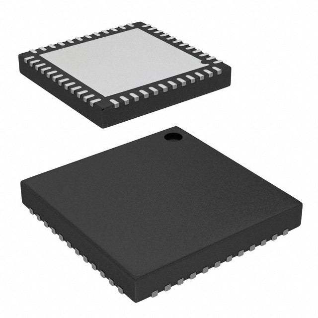
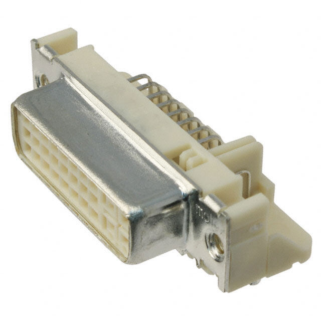
| 产品图片 |
|
| rohs | 符合RoHS |
| 产品系列 | 时钟和计时器IC,时钟发生器及支持产品,IDT 9LPRS436CKILF |
| 产品型号 | 9LPRS436CKILF |
| 产品种类 | 时钟发生器及支持产品 |
| 商标 | IDT |
| 安装风格 | SMD/SMT |
| 封装 | Tube |
| 封装/箱体 | VFQFPN-48 |
| 工作电源电压 | 3.3 V |
| 工作电源电流 | 115 mA |
| 工厂包装数量 | 490 |
| 最大工作温度 | + 85 C |
| 最大输入频率 | 27 MHz |
| 最小工作温度 | - 40 C |
| 类型 | Clock Generators |
| 系列 | 9LPRS436 |
| 输出端数量 | 14 |
| 零件号别名 | 9LPRS436 ICS9LPRS436CKILF |


- 商务部:美国ITC正式对集成电路等产品启动337调查
- 曝三星4nm工艺存在良率问题 高通将骁龙8 Gen1或转产台积电
- 太阳诱电将投资9.5亿元在常州建新厂生产MLCC 预计2023年完工
- 英特尔发布欧洲新工厂建设计划 深化IDM 2.0 战略
- 台积电先进制程称霸业界 有大客户加持明年业绩稳了
- 达到5530亿美元!SIA预计今年全球半导体销售额将创下新高
- 英特尔拟将自动驾驶子公司Mobileye上市 估值或超500亿美元
- 三星加码芯片和SET,合并消费电子和移动部门,撤换高东真等 CEO
- 三星电子宣布重大人事变动 还合并消费电子和移动部门
- 海关总署:前11个月进口集成电路产品价值2.52万亿元 增长14.8%


PDF Datasheet 数据手册内容提取
DATASHEET Low Power Clock for Intel Atom®-Based Systems 9LPRS436C Recommended Application: Key Specifications: NM10 Express Chipset + N450/D410/D510 Atom® CPUs (cid:129) CPU outputs cycle-cycle jitter < 85ps (cid:129) PCIEX outputs cycle-cycle jitter < 125ps Output Features: (cid:129) SATA outputs cycle-cycle jitter < 125ps (cid:129) 2 - 0.8V push-pull differential CPU pairs (cid:129) PCI outputs cycle-cycle jitter < 500ps (cid:129) 2 - 0.8V push-pull differential PCIEX pairs (cid:129) +/- 100ppm frequency accuracy on all clocks (cid:129) 1 - 0.8V push-pull differential SATA75 pair (cid:129) 1 - 0.8V push-pull differential DOT96 pair Features/Benefits: (cid:129) 1 - 0.8V push-pull differential CPU/PCIEX selectable pair (cid:129) VDDSUSP allows 25MHz to run in S-states (cid:129) 1 - PCI (33MHz) (cid:129) Supports programmable spread percentage (cid:129) 1 - PCICLK_F, (33MHz) free-running (cid:129) Uses external 25MHz crystal, external crystal load caps (cid:129) 1 - USB, 48MHz are required for frequency tuning (cid:129) 1 - 12/48MHz (cid:129) PEREQ# pins to support PCIEX/SATA power management. (cid:129) 1 - 25MHz (cid:129) Low power differential clock outputs (No 50Ω resistor to (cid:129) 1 - REF, 14.318MHz GND needed) (cid:129) 1 - 12.288MHz (cid:129) Integrated 33Ω series resistor on all differential outputs. Pin Configuration **FS3/12_288M_2x 1 48 GND VDD12_2882 47 GND PEREQ1#3 46 REF0_2x/FSLC PEREQ2#4 45 VDD14 **FS4/PCICLK0_2x 5 44 Vtt_PwrGd/WOL_STOP# GND6 43 VDDSUSP VDDPCI 7 42 25MHz **ITP_EN/PCICLK_F0_2x 8 41 GND PEREQ3#9 40 X1_25 *SEL12_48#/12_48MHz_2x 10 6 39 X2_25 3 VDD11 38 PCI&PCIEX_STOP# 4 FSLA/USB48_2x 12 S 37 CPU_STOP# R GND13 36 SDATA P DOTT_96MHzLR14 L 35 SCLK DOTC_96MHzLR15 9 34 GND FSLB 16 33 CPUT_LR0 GNDSATA 17 32 CPUC_LR0 SATAT_LR/PCIeT_LR318 31 VDDCPU SATAC_LR/PCIeC_LR319 30 CPUT_LR1 VDDSATA 20 29 CPUC_LR1 PCIeT_LR021 28 CPUITPT_LR2/PCIeT_LR2 PCIeC_LR022 27 CPUITPC_LR2/PCIeC_LR2 PCIeT_LR123 26 VDDPCIEX PCIeC_LR124 25 GND 48-TSSOP * Internal Pull-Up Resistor ** Internal Pull-Down Resistor IDT® Low Power Clock for Intel Atom®-Based Systems 1561C —08/24/11 1
9LPRS436C Low Power Clock for Intel Atom®-Based Systems # P O T # S P _ O C OL ST GND GND REF0_2x/FSL VDD14 Vtt_PwrGd/W VDDSUSP 25MHz GND X1_25 X2_25 PCI&PCIEX_ CPU_STOP# 48 47 46 45 44 43 42 41 40 39 38 37 **FS3/12_288M_2x 1 36 SDATA VDD12_288 2 35 SCLK PEREQ1# 3 34 GND PEREQ2# 4 33 CPUT_LR0 9LPRS436 **FS4/PCICLK0_2x 5 32 CPUC_LR0 GND 6 48 MLF 31 VDDCPU VDDPCI 7 6x6mm 30 CPUT_LR1 **ITP_EN/PCICLK_F0_2x 8 0.4mm pitch 29 CPUC_LR1 PEREQ3# 9 28 CPUITPT_LR2/PCIeT_LR2 *SEL12_48#/12_48MHz_2x 10 27 CPUITPC_LR2/PCIeC_LR2 VDD 11 26 VDDPCIEX FSLA/USB48_2x 12 25 GND 13 14 15 16 17 18 19 20 21 22 23 24 GND T_96MHzLR C_96MHzLR FSLB GNDSATA PCIeT_LR3 PCIeC_LR3 VDDSATA PCIeT_LR0 PCIeC_LR0 PCIeT_LR1 PCIeC_LR1 OT OT R/ R/ D D _L _L T C A A T T A A S S * Internal Pull-Up Resistor ** Internal Pull-Down Resistor IDT® Low Power Clock for Intel Atom®-Based Systems 1561C — 08/24/11 2
9LPRS436C Low Power Clock for Intel Atom®-Based Systems Pin Description PIN # PIN NAME TYPE DESCRIPTION 1 **FS3/12_288M_2x I/O Frequency select latch input pin / 12.288MHz output, 3.3V 2 VDD12_288 PWR Power for 12.288MHz PLL and output buffer, nominal 3.3V. Real-time input pin that controls SATACLK and PCIEXCLK outputs that are 3 PEREQ1# IN selected through the SMBus. 1 = selected outputs are disabled, 0 = selected outputs are enabled. Real-time input pin that controls SATACLK and PCIEXCLK outputs that are 4 PEREQ2# IN selected through the SMBus. 1 = selected outputs are disabled, 0 = selected outputs are enabled. 5 **FS4/PCICLK0_2x I/O Frequency select latch input pin / 3.3V PCI clock output. 6 GND PWR Ground pin. 7 VDDPCI PWR Power supply for PCI clocks, nominal 3.3V ITP Enable Latched Input/Free Running PCI clock output. ITP_Enable Selects the functionality of the CPU_ITP/SRC output as follows: 8 **ITP_EN/PCICLK_F0_2x I/O 1 = CPU_ITP output 0 = SRC output Real-time input pin that controls PCIEXCLK outputs that are selected through 9 PEREQ3# IN the SMBus. 1 = selected outputs are disabled, 0 = selected outputs are enabled. Latched select input for 12/48MHz output. 1=12MHz, 0=48MHz. 12/48MHz 10 *SEL12_48#/12_48MHz_2x I/O clock output. 11 VDD PWR Power supply, nominal 3.3V 3.3V tolerant input for CPU frequency selection. Low voltage threshold inputs, 12 FSLA/USB48_2x I/O see input electrical characteristics for Vil_FS and Vih_FS values. / 48.00MHz USB clock 13 GND PWR Ground pin. True clock of low power differential pair for 96.00MHz DOT clock. No 50ohm 14 DOTT_96MHzLR OUT to GND needed. No Rs needed. Complementary clock of low power differential pair for 96.00MHz DOT clock. 15 DOTC_96MHzLR OUT No 50ohm resistor to GND needed. No Rs needed. 3.3V tolerant input for CPU frequency selection. Refer to input electrical 16 FSLB IN characteristics for Vil_FS and Vih_FS values. 17 GNDSATA PWR Ground pin for the SATA outputs True clock of differential SATA pair. / True clock of differential PCI-Express pair 18 SATAT_LR/PCIeT_LR3 OUT - selectable by FS(4:3) ; both are 0.8V differential push pull outputs with integrated 33ohm series resistor. Complementary clock of differential SATA pair. / Complementary clock of 19 SATAC_LR/PCIeC_LR3 OUT differential PCI-Express pair - selectable by FS(4:3); both are 0.8V differential push pull outputs with integrated 33ohm series resistor. 20 VDDSATA PWR Supply for SATA clocks, 3.3V nominal True clock of 0.8V differential push-pull PCI_Express pair with integrated 21 PCIeT_LR0 OUT 33ohm series resistor Complementary clock of 0.8V differential push-pull PCI_Express pair with 22 PCIeC_LR0 OUT integrated 33ohm series resistor True clock of 0.8V differential push-pull PCI_Express pair with integrated 23 PCIeT_LR1 OUT 33ohm series resistor Complementary clock of 0.8V differential push-pull PCI_Express pair with 24 PCIeC_LR1 OUT integrated 33ohm series resistor IDT® Low Power Clock for Intel Atom®-Based Systems 1561C — 08/24/11 3
9LPRS436C Low Power Clock for Intel Atom®-Based Systems Pin Description (Continued) 25 GND PWR Ground pin. 26 VDDPCIEX PWR Power supply for PCI Express clocks, nominal 3.3V Complementary clock of differential pair CPU output. / Complementary clock of 27 CPUITPC_LR2/PCIeC_LR2 OUT differential PCIEX pair. These are 0.8V push pull outputs. No external 50ohm resistor to GND or 33ohm series resistor needed. True clock of differential pair CPU output. / True clock of differential PCIEX 28 CPUITPT_LR2/PCIeT_LR2 OUT pair. These are 0.8V push pull outputs. No external 50ohm resistor to GND or 33ohm series resistor needed. Complementary clock of differential pair 0.8V push-pull CPU outputs with 29 CPUC_LR1 OUT integrated 33ohm series resistor. True clock of differential pair 0.8V push-pull CPU outputs with integrated 30 CPUT_LR1 OUT 33ohm series resistor. 31 VDDCPU PWR Supply for CPU clocks, 3.3V nominal Complementary clock of differential pair 0.8V push-pull CPU outputs with 32 CPUC_LR0 OUT integrated 33ohm series resistor. True clock of differential pair 0.8V push-pull CPU outputs with integrated 33 CPUT_LR0 OUT 33ohm series resistor. 34 GND PWR Ground pin. 35 SCLK IN Clock pin of SMBus circuitry, 5V tolerant. 36 SDATA I/O Data pin for SMBus circuitry, 5V tolerant. 37 CPU_STOP# IN Stops CPU0 clock when enabled. Stops all PCICLKs at logic 0 level, when low. Free running PCICLKs are not 38 PCI&PCIEX_STOP# IN effected by this input. 39 X2_25 OUT Crystal output, Nominally 25.00MHz. 40 X1_25 IN Crystal input, Nominally 25.00MHz. 41 GND PWR Ground pin. 42 25MHz OUT 25MHz clock output, 3.3V Supply for suspend mode, powers 25MHz PLL, 25M output and XTAL 43 VDDSUSP PWR oscillator. 3.3V Nominal This active high 3.3V LVTTL input is a level sensitive strobe used to determine 44 Vtt_PwrGd/WOL_STOP# IN when latch inputs are valid and are ready to be sampled / Asynchronous active low input pin that stops all outputs except free running 25Mhz 45 VDD14 PWR Power for 14.31818MHz PLL and REF output, nominal 3.3V. 2x strength 14.318 MHz reference clock./ 3.3V tolerant input for CPU frequency 46 REF0_2x/FSLC I/O selection. Refer to input electrical characteristics for Vil_FS and Vih_FS values. 47 GND PWR Ground pin. 48 GND PWR Ground pin. IDT® Low Power Clock for Intel Atom®-Based Systems 1561C — 08/24/11 4
9LPRS436C Low Power Clock for Intel Atom®-Based Systems General Description The 9LPRS436C is a low power CK505-compatible clock targeted at Intel-based Netbooks and Nettops. This clock synthesizer provides a single chip solution for systems using the Intel NM10 chipset paired with the Intel N450/D410/D510 Atom® CPUs. The 9LPRS436C is driven with a 25MHz crystal. Block Diagram 25M NonSS 14.318M PLL NonSS 12.288M PLL CPU 25M SS PLL PCI XTAL PCIe/ SATA 75M/ 100M NonSS DOT96 PLL 48MHz 12_48MHz Series Resistors for Single Ended Outputs Number of Number of Loads Actually Driven. Match Point for N & P Loads 1 Load 2 Loads 3 Loads Voltage / Current (mA) D.C.Drive Strength to Drive Rs= Rs= Rs= 1 0.56 / 33 (17Ω) 33Ω [39Ω] - - 2 0.92 / 66 (14Ω) 39Ω [43Ω] 22Ω [27Ω] - Notes: 1. Preferred drive strengths using CK505 clock sources. Transmission lines to load do not share series resistors. 2. Desktop/Mobile Platforms with Zo = 50/55 ohms use the first resistor value. 3. Systems with Zo = 60 ohms use the resistor values in brackets [ ]. IDT® Low Power Clock for Intel Atom®-Based Systems 1561C — 08/24/11 5
9LPRS436C Low Power Clock for Intel Atom®-Based Systems Table 1: CPU/SRC/PCI PLL Spread Frequency Selection Table for 9LPRS436C FS4 FS3 FS C FS B FS A CPU L L L SRC PCI SATA (B0b4) (B0b3) (B0b2) (B0b1) (B0b0) MHz 0 0 0 0 0 0 100.00 100.00 33.33 Follows SRC 1 0 0 0 0 1 100.00 100.00 33.33 Follows SRC 2 0 0 0 1 0 83.33 100.00 33.33 Follows SRC 3 0 0 0 1 1 83.33 100.00 33.33 Follows SRC 4 0 0 1 0 0 133.33 100.00 33.33 Follows SRC 5 0 0 1 0 1 133.33 100.00 33.33 Follows SRC 6 0 0 1 1 0 166.67 100.00 33.33 Follows SRC 7 0 0 1 1 1 166.67 100.00 33.33 Follows SRC 8 0 1 0 0 0 100.00 100.00 33.33 100MHz Non-Spread 9 0 1 0 0 1 100.00 100.00 33.33 100MHz Non-Spread 10 0 1 0 1 0 83.33 100.00 33.33 100MHz Non-Spread 11 0 1 0 1 1 83.33 100.00 33.33 100MHz Non-Spread 12 0 1 1 0 0 133.33 100.00 33.33 100MHz Non-Spread 13 0 1 1 0 1 133.33 100.00 33.33 100MHz Non-Spread 14 0 1 1 1 0 166.67 100.00 33.33 100MHz Non-Spread 15 0 1 1 1 1 166.67 100.00 33.33 100MHz Non-Spread 16 1 0 0 0 0 100.00 100.00 33.33 75MHz Non-Spread 17 1 0 0 0 1 100.00 100.00 33.33 75MHz Non-Spread 18 1 0 0 1 0 83.33 100.00 33.33 75MHz Non-Spread 19 1 0 0 1 1 83.33 100.00 33.33 75MHz Non-Spread 20 1 0 1 0 0 133.33 100.00 33.33 75MHz Non-Spread 21 1 0 1 0 1 133.33 100.00 33.33 75MHz Non-Spread 22 1 0 1 1 0 166.67 100.00 33.33 75MHz Non-Spread 23 1 0 1 1 1 166.67 100.00 33.33 75MHz Non-Spread 24 1 1 0 0 0 100.00 100.00 33.33 75MHz Non-Spread 25 1 1 0 0 1 100.00 100.00 33.33 75MHz Non-Spread 26 1 1 0 1 0 83.33 100.00 33.33 75MHz Non-Spread 27 1 1 0 1 1 83.33 100.00 33.33 75MHz Non-Spread 28 1 1 1 0 0 133.33 100.00 33.33 75MHz Non-Spread 29 1 1 1 0 1 133.33 100.00 33.33 75MHz Non-Spread 30 1 1 1 1 0 166.67 100.00 33.33 75MHz Non-Spread 31 1 1 1 1 1 166.67 100.00 33.33 75MHz Non-Spread IDT® Low Power Clock for Intel Atom®-Based Systems 1561C — 08/24/11 6
9LPRS436C Low Power Clock for Intel Atom®-Based Systems Table 2: Slew Rate Selection Table Slew Bit 1 Bit 0 Rate 0 0 Hi-Z 0.6X 0 1 (1.2V/ns) 0.8X 1 0 (1.6V/ns) 1X 1 1 (2.0V/ns) CPU Power Management Table SMBus PCI&PCIEX_ WOL_STOP# CPU_STOP# CPU(1:0)/ITP CPU#(1:0)/ITP Register OE STOP# 1 Enable 1 X Running Running 1 Enable 0 X High Low 0 Enable X X Low Low X Disable X X Low Low Differential Power Management Table SMBus PCI&PCIEX_ PCIEX/SATA PCIEX/SATA# PCIEX/SATA PCIEX/SATA# WOL_STOP# CPU_STOP# DOT DOT# Register OE STOP# PCI Stoppable Free-Run 1 Enable X 1 Running Running Running Running Running Running 1 Enable X 0 High Low Running Running Running Running 0 Enable X X Low Low Low/20K Low Low/20K Low X Disable X X Low Low Low/20K Low Low/20K Low Singled-ended Power Management Table SMBus PCI&PCIEX_ PCIF/PCI PCIF/PCI 12/48MHz 25MHz 25MHz WOL_STOP# CPU_STOP# REF Register OE STOP# Free-run Stoppable 12.288MHz Free-run Stoppable 1 Enable X 1 Running Running Running Running Running Running 1 Enable X 0 Running Low Running Running Running Running 0 Enable X X Low Low Low Low Running Low X Disable X X Low Low Low Low Low Low PEREQ# Control Table: PCIe PEREQ# controlled 1 0, SATA/PCIe3 2 SATA/PCIe3, 1 3 1, 2 IDT® Low Power Clock for Intel Atom®-Based Systems 1561C — 08/24/11 7
9LPRS436C Low Power Clock for Intel Atom®-Based Systems Electrical Characteristics - Absolute Maximum Ratings PARAMETER SYMBOL CONDITIONS MIN TYP MAX UNITS NOTES 3.3V Core Supply Voltage VDDA 4.6 V 1,2 3.3V Logic Supply Voltage VDD 4.6 V 1,2 Input Low Voltage VIL GND-0.5 V 1 Input High Voltage VIH Except for SMBus interface VDD+0.5V V 1 Input High Voltage V SMBus clock and data pins 5.5V V 1 IHSMB Storage Temperature Ts -65 150 °C 1 Case Temperature Tcase 115 °C 1 Input ESD protection ESD prot Human Body Model 2000 V 1 1Guaranteed by design and characterization, not 100% tested in production. 2 Operation under these conditions is neither implied nor guaranteed. Electrical Characteristics - Input/Supply/Common Output DC Parameters PARAMETER SYMBOL CONDITIONS MIN TYP MAX UNITS Notes T Standard Device 0 85 °C Ambient Operating Temp ambC T Industrial Temperature Range Device -40 85 °C ambI Supply Voltage VDDxxx Supply Voltage 3.135 3.465 V Input High Voltage V Single-ended 3.3V inputs 2 V + 0.3 V 7 IHSE DD Input Low Voltage V Single-ended 3.3V inputs V - 0.3 0.8 V 7 ILSE SS FS(4:3) Input High Voltage VIH_FS4 Single-ended 3.3V FS(4:3) Inputs 2 VDD + 0.3 V FS(4:3) Input Low Voltage VIL_FS4 Single-ended 3.3V FS(4:3) Inputs VSS - 0.3 0.8 V Low Threshold Input- High Voltage VIH_FS 3.3 V +/-5% 0.7 VDD+0.3 V Low Threshold Input- V 3.3 V +/-5% V - 0.3 0.35 V Low Voltage IL_FS SS Input Leakage Current IIN VIN = VDD , VIN = GND -5 5 uA 6 Inputs with pull up or pull down resistors Input Leakage Current IINRES V = V V =GND -200 200 uA IN DD , IN Output High Voltage VOHSE Single-ended outputs, IOH = -1mA 2.4 V 5 Output Low Voltage V Single-ended outputs, I = 1 mA 0.4 V 5 OLSE OL Operating Supply Current IDDVDD3.3 Full Active, CL = Full load; IDD 3.3V 106 115 mA I Full Active, C = Full load; IDD 3.3V 12 15 mA DDVDDSUSP3.3 L IDDPDVDD3.3 3.3V Main Rail 0 mA Powerdown Current I VDD_SUSP Rail. 25MHz Running (WOL) 12 15 mA DDPDSUSP3.3w IDDPDSUSP3.3 VDD_SUSP Rail. 25MHz Off 3 4 mA Input Frequency Fi VDD = 3.3 V 27 MHz 8 Pin Inductance Lpin 7 nH CIN Logic Inputs 1.5 5 pF Input Capacitance COUT Output pin capacitance 6 pF C X1 & X2 pins 6 pF INX SMBus Voltage V 2.7 5.5 V DD Low-level Output Voltage V @ I 0.4 V OLSMB PULLUP Current sinking at VOLSMB = 0.4 V IPULLUP SMB Data Pin 4 mA SCLK/SDATA (Max VIL - 0.15) to Clock/Data Rise Time TRI2C (Min VIH + 0.15) 1000 ns SCLK/SDATA (Min VIH + 0.15) to Clock/Data Fall Time TFI2C (Max VIL - 0.15) 300 ns Maximum SMBus Operating Frequency F 100 kHz SMBUS Spread Spectrum Modulation Frequency fSSMOD Triangular Modulation 30 32.5 33 kHz NOTES on DC Parameters: (unless otherwise noted, guaranteed by design and characterization, not 100% tested in production). 1 Operation at these points is not recommended 2 Maximum VIH is not to exceed VDD 3 Human Body Model 4 Operation under these conditions is neither implied, nor guaranteed. 5Signal is required to be monotonic in this region. 6 Input leakage current does not include inputs with pull-up or pull-down resistors 7 3.3V referenced inputs are: PCI&PCIEX_STOP#, CPU_STOP#, ITP_EN, SCLK, SDATA, VTT_PWR_GD/PD#, SEL12_48# and PEREQ# inputs if selected. 8 For margining purposes only. Normal operation should have Fin = 25MHz +/-50ppm IDT® Low Power Clock for Intel Atom®-Based Systems 1561C — 08/24/11 8
9LPRS436C Low Power Clock for Intel Atom®-Based Systems AC Electrical Characteristics - Input/Common Parameters PARAMETER SYMBOL CONDITIONS MIN TYP MAX UNITS Notes From VDD Power-Up or de-assertion of PD to Clk Stabilization TSTAB 1st clock 1.1 1.8 ms Tdrive_PEREQ_off T Output stop after PEREQ# deasserted 2 3 clocks DRPEROFF Tdrive_PEREQ_on T Output run after PEREQ# asserted 2 3 clocks DRPERON CPU output enable after Tdrive_CPU TDRSRC CPU_STOP# de-assertion 8 10 ns PCIEX output enable after Tdrive_PCIEX T 8 15 ns 1 DRPCIEX PCI&PCIEX_STOP# de-assertion Tfall_SE TFALL Fall/rise time of all 3.3V control inputs from 20- 10 ns Trise_SE TRISE 80% 10 ns Differential output enable after Tdrive_PD# TDRPD PD# de-assertion 85 300 us 1 AC Electrical Characteristics - CPU, PCIEX, SATA, DOT96MHz PARAMETER SYMBOL CONDITIONS MIN TYP MAX UNITS NOTES Rising Edge Slew Rate tSLR Differential Measurement 2.5 3.3 4 V/ns 1,2 Falling Edge Slew Rate tFLR Differential Measurement 2.5 3.2 4 V/ns 1,2 Slew Rate Variation tSLVAR Single-ended Measurement 16 20 % 1 Maximum Output Voltage VHIGH Includes overshoot 806 1150 mV 1 Minimum Output Voltage VLOW Includes undershoot -300 mV 1 Differential Voltage Swing VSWING Differential Measurement 300 mV 1 Crossing Point Voltage VXABS Single-ended Measurement 300 395 550 mV 1,3,4 Crossing Point Variation VXABSVAR Single-ended Measurement 32 140 mV 1,3,5 Duty Cycle DCYC Differential Measurement 45 49.7 55 % 1 CPU Jitter - Cycle to Cycle CPUJC2C Differential Measurement 66 85 ps 1 CPU2_IPT Jitter - Cycle to Cycle CPU2JC2C Differential Measurement 125 150 ps 1 SRC Jitter - Cycle to Cycle SRCJC2C Differential Measurement 66 125 ps 1 SATA Jitter - Cycle to Cycle SATAJC2C Differential Measurement 66 125 ps 1 DOT Jitter - Cycle to Cycle DOTJC2C Differential Measurement 65 250 ps 1 CPU[1:0] Skew CPUSKEW10 Differential Measurement 38 100 ps 1,6 CPU[2_ITP:0] Skew CPUSKEW20 Differential Measurement 145 150 ps 1,6 SRC Skew SRCSKEW Differential Measurement 44 250 ps 1 Electrical Characteristics - PCICLK/PCICLK_F PARAMETER SYMBOL CONDITIONS MIN TYP MAX UNITS NOTES Output Impedance RDSP VO = VDD*(0.5) 12 55 Ω 1 Long Accuracy ppm see Tperiod min-max values -100 100 ppm 2 33.33MHz output no spread 29.99700 30.00300 ns 2 Clock period Tperiod 33.33MHz output spread 30.08421 30.23459 ns 2 33.33MHz output no spread 29.49700 30.50300 ns 2 Absolute min/max period Tabs 33.33MHz output nominal/spread 29.56617 30.58421 ns 2 Output High Voltage VOH IOH = -1 mA 2.4 V 1 Output Low Voltage V I = 1 mA 0.4 V 1 OL OL Output High Current I V OH @MIN = 1.0 V -33 mA 1 OH VOH@MAX = 3.135 V -33 mA 1 Output Low Current I VOL @ MIN = 1.95 V 30 mA 1 OL VOL @ MAX = 0.4 V 38 mA 1 Rising Edge Slew Rate tSLR Measured from 0.8 to 2.0 V 1 1.7 4 V/ns 1 Falling Edge Slew Rate tFLR Measured from 2.0 to 0.8 V 1 1.8 4 V/ns 1 Duty Cycle dt1 VT = 1.5 V 45 50.6 55 % 1 Pin to Pin Skew tskew VT = 1.5 V 250 ps 1 Jitter, Cycle to cycle tjcyc-cyc VT = 1.5 V 150 500 ps 1 *TA = Tambient; VDD = 3.3 V +/-5%; CL=5pF, Rs=22Ω (unless specified otherwise) 1 Guaranteed by design and characterization, not 100% tested in production. 2 All Long Term Accuracy and Clock Period specifications are guaranteed assuming that REFOUT is at 14.31818MHz 3 Slew rate emastured through V_swing voltage range centered about differential zero 4 Vcross is defined at the voltage where Clock = Clock#. 5 Only applies to the differential rising edge (Clock rising, Clock# falling.) 6 CPU group skew is nominally 0ps. IDT® Low Power Clock for Intel Atom®-Based Systems 1561C — 08/24/11 9
9LPRS436C Low Power Clock for Intel Atom®-Based Systems Electrical Characteristics - USB48MHz, 12/48MHz PARAMETER SYMBOL CONDITIONS MIN TYP MAX UNITS NOTES Long Accuracy ppm see Tperiod min-max values -100 100 ppm 1,2 Clock period Tperiod 48.00MHz output nominal 20.83125 20.83542 ns 2,3 Absolute min/max period Tabs 48.00MHz output nominal 20.48125 21.18542 ns 2 Output High Voltage V I = -1 mA 2.4 V 1 OH OH Output Low Voltage VOL IOL = 1 mA 0.4 V 1 Rising Edge Slew Rate (USB48M) tSLR Measured from 0.8 to 2.0 V 1 1.7 2 V/ns 1 Falling Edge Slew Rate (USB48M) tFLR Measured from 2.0 to 0.8 V 1 1.7 2 V/ns 1 Rising Edge Slew Rate (12/48M) tSLR Measured from 0.8 to 2.0 V 1 1.7 2 V/ns 1 Falling Edge Slew Rate (12/48M) tFLR Measured from 2.0 to 0.8 V 1 1.7 2 V/ns 1 Duty Cycle dt1 VT = 1.5 V 45 50.6 55 % 1 Jitter, Cycle to cycle tjcyc-cyc VT = 1.5 V 150 350 ps 1 Electrical Characteristics - 25MHz PARAMETER SYMBOL CONDITIONS MIN TYP MAX UNITS NOTES Long Accuracy ppm see Tperiod min-max values -100 0 100 ppm 1,2 Clock period T 25.00MHz output nominal 39.99600 40.00400 ns 2,3 period Absolute min/max period Tabs 25.00MHz output nominal 39.32360 40.67640 ns 2 Output High Voltage V I = -1 mA 2.4 V 1 OH OH Output Low Voltage V I = 1 mA 0.4 V 1 OL OL Rising Edge Slew Rate t Measured from 0.8 to 2.0 V 1 1.8 2 V/ns 1 SLR Falling Edge Slew Rate t Measured from 2.0 to 0.8 V 1 1.8 2 V/ns 1 FLR Duty Cycle d V = 1.5 V 45 49.6 55 % 1 t1 T Jitter, Cycle to cycle t V = 1.5 V 150 500 ps 1 jcyc-cyc T Electrical Characteristics - 12.288MHz PARAMETER SYMBOL CONDITIONS MIN TYP MAX UNITS NOTES Long Accuracy ppm see Tperiod min-max values -100 0 100 ppm 1,2 Clock period T 12.288MHz output nominal 81.37207 81.38835 ns 2,3 period Absolute min/max period Tabs 12.288MHz output nominal 80.87207 81.88835 ns 2 Output High Voltage V I = -1 mA 2.4 V 1 OH OH Output Low Voltage V I = 1 mA 0.4 V 1 OL OL Rising Edge Slew Rate t Measured from 0.8 to 2.0 V 1 1.8 2 V/ns 1 SLR Falling Edge Slew Rate t Measured from 2.0 to 0.8 V 1 1.8 2 V/ns 1 FLR Duty Cycle d V = 1.5 V 45 50.1 55 % 1 t1 T Jitter, Cycle to cycle t V = 1.5 V 133 500 ps 1 jcyc-cyc T Electrical Characteristics - REF-14.318MHz PARAMETER SYMBOL CONDITIONS MIN TYP MAX UNITS Notes Long Accuracy ppm see Tperiod min-max values -100 0 100 ppm 1,2 Clock period Tperiod 14.318MHz output nominal 69.82033 69.86224 ns 2,3 Absolute min/max period Tabs 14.318MHz output nominal 69.83400 70.84800 ns 2 Output High Voltage VOH IOH = -1 mA 2.4 V 1 Output Low Voltage VOL IOL = 1 mA 0.4 V 1 Rising Edge Slew Rate tSLR Measured from 0.8 to 2.0 V 1 1.5 4 V/ns 1 Falling Edge Slew Rate tFLR Measured from 2.0 to 0.8 V 1 1.4 4 V/ns 1 Duty Cycle dt1 VT = 1.5 V 45 50.2 55 % 1 Jitter, Cycle to cycle tjcyc-cyc VT = 1.5 V 139 1000 ps 1 *TA = Tambient; VDD = 3.3 V +/-5%; CL=5pF, Rs=22Ω (unless specified otherwise) 1 Guaranteed by design and characterization, not 100% tested in production. 2 All Long Term Accuracy and Clock Period specifications are guaranteed assuming that REFOUT is at 14.31818MHz 3 The average period over any 1us period of time Electrical Characteristics - Phase Jitter PARAMETER SYMBOL CONDITIONS MIN TYP. MAX UNITS NOTES t PCIe Gen 1 REFCLK phase jitter 30 86 ps 1,2,3 jphPCIe1 PCIe Gen 2 REFCLK phase jitter ps Jitter, Phase tjphPCIe2Lo Lo-band content 1.3 3 (RMS) 1,2,3 PCIe Gen 2 REFCLK phase jitter ps tjphPCIe2Hi Hi-band content 1.7 3.1 (RMS) 1,2,3 *TA = Tambient; VDD = 3.3 V +/-5%; CL=5pF, Rs=22Ω (unless specified otherwise) Notes on Phase Jitter: 1 See http://www.pcisig.com for complete specs. Guaranteed by design and characterization, not tested in production. 2 Device driven by 932S421BGLF or equivalent 2 Sample size of at least 100K cycles. This figures extrapolates to 108ps pk-pk @ 1M cycles for a BER of 1-12 3 Applies to PCIEX(3:0) outputs only. IDT® Low Power Clock for Intel Atom®-Based Systems 1561C — 08/24/11 10
9LPRS436C Low Power Clock for Intel Atom®-Based Systems Driving LVDS inputs with the 9LPRS436 Value Receiver has Receiver does not Component termination have termination Note R7a, R7b 10K ohm 140 ohm R8a, R8b 5.6K ohm 75 ohm Cc 0.1 uF 0.1 uF Vcm 1.2 volts 1.2 volts 3.3 Volts R7a R7b Cc L4 L4’ Cc 9LPRS436 R8a R8b LVDS CLK Input IDT® Low Power Clock for Intel Atom®-Based Systems 1561C — 08/24/11 11
9LPRS436C Low Power Clock for Intel Atom®-Based Systems General SMBus serial interface information for the 9LPRS436C How to Write: How to Read: • Controller (host) sends a start bit. (cid:129) Controller (host) will send start bit. (cid:129) Controller (host) sends the write address D2 (cid:129) Controller (host) sends the write address D2 (H) (H) (cid:129) ICS clock will acknowledge (cid:129) ICS clock will acknowledge (cid:129) Controller (host) sends the beginning byte location = N (cid:129) Controller (host) sends the begining byte (cid:129) ICS clock will acknowledge location = N (cid:129) Controller (host) sends the data byte count = X (cid:129) ICS clock will acknowledge (cid:129) ICS clock will acknowledge (cid:129) Controller (host) will send a separate start bit. (cid:129) Controller (host) starts sending Byte N through (cid:129) Controller (host) sends the read address D3 (H) Byte N + X -1 (cid:129) ICS clock will acknowledge (cid:129) ICS clock will acknowledge each byte one at a time (cid:129) ICS clock will send the data byte count = X (cid:129) Controller (host) sends a Stop bit (cid:129) ICS clock sends Byte N + X -1 (cid:129) ICS clock sends Byte 0 through byte X (if X (H) was written to byte 8). (cid:129) Controller (host) will need to acknowledge each byte (cid:129) Controller (host) will send a not acknowledge bit (cid:129) Controller (host) will send a stop bit Index Block Write Operation Index Block Read Operation Controller (Host) ICS (Slave/Receiver) Controller (Host) ICS (Slave/Receiver) T starT bit T starT bit Slave Address D2 Slave Address D2 (H) (H) WR WRite WR WRite ACK ACK Beginning Byte = N Beginning Byte = N ACK ACK Data Byte Count = X RT Repeat starT ACK Slave Address D3 (H) Beginning Byte N RD ReaD ACK ACK e yt B Data Byte Count = X X ACK Beginning Byte N Byte N + X - 1 ACK ACK e P stoP bit yt B X Byte N + X - 1 N Not acknowledge P stoP bit IDT® Low Power Clock for Intel Atom®-Based Systems 1561C — 08/24/11 12
9LPRS436C Low Power Clock for Intel Atom®-Based Systems SMBus Table: Frequency Select Register Byte 0 Name Control Function Type 0 1 PWD Bit 7 Reserved 0 Bit 6 Reserved 0 Enables Spread for Bit 5 Spread Enable RW Off 0.5% down spread 0 CPU/SRC/PCI outputs Bit 4 FS4 Freq Select Bit 4 RW Latch Bit 3 FS3 Freq Select Bit 3 RW Latch See Table 1: CPU/SRC/PCI PLL Bit 2 FSLC Freq Select Bit 2 RW Latch Frequency Selection Table Bit 1 FSLB Freq Select Bit 1 RW Latch Bit 0 FSLA Freq Select Bit 0 RW Latch SMBus Table: Output Control Register Byte 1 Name Control Function Type 0 1 PWD Bit 7 DOT96Mhz Output Enable RW Disable Enable 1 Bit 6 SATA/PCIe3 Output Enable RW Disable Enable 1 Bit 5 ITP/PCIe2 Output Enable RW Disable Enable 1 Bit 4 PCIe1 Output Enable RW Disable Enable 1 Bit 3 PCIe0 Output Enable RW Disable Enable 1 Output Enable (Disabling This Bit 2 12.288MHz output also disables the RW Disable Enable 1 12.288M PLL). 25MHz free running during VDD Suspend (S-states). If this bit is Bit 1 25MHz set to 0, the XTAL OSC will also RW Does Not Run Runs 1 be powered down in the Suspend States) Bit 0 CPU PLL MN_EN CPU PLL M/N Enable RW Disable Enable 0 SMBus Table: Output Control Register Byte 2 Name Control Function Type 0 1 PWD Bit 7 USB_48MHz Output Enable RW Disable Enable 1 Bit 6 Reserved 0 Bit 5 REF0 Output Enable RW Disable Enable 1 Bit 4 25MHz Output Enable RW Disable Enable 1 Bit 3 12_48MHz Output Enable RW Disable Enable 1 Bit 2 PCICLK_F0 Output Enable RW Disable Enable 1 Bit 1 PCICLK0 Output Enable RW Disable Enable 1 Bit 0 Reserved 0 SMBus Table: Output Control Register Byte 3 Name Control Function Type 0 1 PWD Bit 7 CPUCLK1 Output Enable RW Disable Enable 1 Bit 6 CPUCLK0 Output Enable RW Disable Enable 1 Bit 5 PEREQ3# Control PCIEX1 is controlled RW Not Controlled Controlled 0 Bit 4 PEREQ3# Control PCIEX2 is controlled RW Not Controlled Controlled 0 Bit 3 PEREQ2# Control PCIEX1 is controlled RW Not Controlled Controlled 0 Bit 2 PEREQ2# Control SATACLK is controlled RW Not Controlled Controlled 0 Bit 1 PEREQ1# Control PCIEX0 is controlled RW Not Controlled Controlled 0 Bit 0 PEREQ1# Control SATACLK is controlled RW Not Controlled Controlled 0 NOTE: Only 1 PEREQ at a time can be selected to control an output. IDT® Low Power Clock for Intel Atom®-Based Systems 1561C — 08/24/11 13
9LPRS436C Low Power Clock for Intel Atom®-Based Systems SMBus Table: Output Control and Readback Register Byte 4 Name Control Function 0 1 PWD Bit 7 Reserved 0 Bit 6 CPU_1 Free-Running Control RW Free-Running Stoppable 0 Bit 5 SEL_12_48 SEL12_48MHz readback R 48MHz 12MHz latch Bit 4 CPUCLK_2/ITP Free-Running Control RW Free-Running Stoppable 0 Bit 3 ITP_EN ITP_EN readback R PCIEX6 CPU_ITP latch Bit 2 Reserved 0 Bit 1 CPUCLK_0 Free-Running Control RW Free-Running Stoppable 0 Bit 0 Reserved 0 SMBus Table: Output Control Register Byte 5 Name Control Function 0 1 PWD Bit 7 Reserved 0 Bit 6 Reserved 0 Bit 5 Reserved 0 Bit 4 SATA/PCIe3 Free- Running Control RW Free-Running Stoppable 1 Bit 3 PCIe2 Free- Running Control RW Free-Running Stoppable 0 Bit 2 PCIe1 Free- Running Control RW Free-Running Stoppable 0 Bit 1 PCIe0 Free- Running Control RW Free-Running Stoppable 0 Bit 0 Load Control IIC Load control RW Load Do not Load 0 SMBus Table: Amplitude Control Register Byte 6 Name Control Function Type 0 1 PWD Bit 7 Diff AMP PCIe(2:0) Differential output RW 00 = 700mV 10 = 900mV 0 Bit 6 Diff AMP Amplitude Control RW 01 = 800mV 11 = 1000mV 1 Bit 5 Diff AMP DOT96 Differential output RW 00 = 700mV 10 = 900mV 0 Bit 4 Diff AMP Amplitude Control RW 01 = 800mV 11 = 1000mV 1 Bit 3 Diff AMP SATA/PCIe3 Differential output RW 00 = 700mV 10 = 900mV 0 Bit 2 Diff AMP Amplitude Control RW 01 = 800mV 11 = 1000mV 1 Bit 1 Diff AMP CPU Differential output RW 00 = 700mV 10 = 900mV 0 Bit 0 Diff AMP Amplitude Control RW 01 = 800mV 11 = 1000mV 1 SMBus Table: Revision and Vendor ID Register Byte 7 Name Control Function Type 0 1 PWD Bit 7 RID3 R x Bit 6 RID2 R x Revision ID 0010 = C Rev Bit 5 RID1 R x Bit 4 RID0 R x Bit 3 VID3 R 0 Bit 2 VID2 R 0 VENDOR ID 0001 = ICS Bit 1 VID1 R 0 Bit 0 VID0 R 1 IDT® Low Power Clock for Intel Atom®-Based Systems 1561C — 08/24/11 14
9LPRS436C Low Power Clock for Intel Atom®-Based Systems SMBus Table: Byte Count Register Byte 8 Name Control Function Type 0 1 PWD Bit 7 Reserved 0 Bit 6 Reserved 0 Bit 5 Reserved 0 Bit 4 BC4 RW 0 Bit 3 BC3 RW Writing to this register will configure how 1 Bit 2 BC2 Byte Count Programming RW many bytes will be read back, default is 1 Bit 1 BC1 RW 0F = 15 bytes. 1 Bit 0 BC0 RW 1 SMBus Table: Watch Dog Timer Control Register Byte 9 Name Control Function Type 0 1 PWD Bit 7 HWD_EN Watchdog Hard Alarm Enable RW Disable Enable 0 Bit 6 WD Hard Status WD Hard Alarm Status R Normal Alarm X Watch Dog Alarm Time base Bit 5 WDTCtrl R 290ms Base 0 Control Bit 4 HWD3 WD Hard Alarm Timer Bit 3 RW These bits represent X*290ms or X*1.16s. 1 Bit 3 HWD2 WD Hard Alarm Timer Bit 2 RW The watchdog timer waits before it goes to 1 Bit 2 HWD1 WD Hard Alarm Timer Bit 1 RW alarm mode. Default is 15 X 290ms = 1 Bit 1 HWD0 WD Hard Alarm Timer Bit 0 RW 4.35s. 1 Bit 0 Reserved Reserved RW - - 0 SMBus Table: Skew programming Register Byte 10 Name Control Function Type 0 1 PWD Bit 7 CPUSkw3 RW 0 Bit 6 CPUSkw2 RW 0 CPUCLK0 Skew Control (ps) See CPU Skew Programming Table Bit 5 CPUSkw1 RW 0 Bit 4 CPUSkw0 RW 0 Bit 3 CPUSkw3 RW 0 Bit 2 CPUSkw2 RW 0 CPUCLK1 Skew Control (ps) See CPU Skew Programming Table Bit 1 CPUSkw1 RW 0 Bit 0 CPUSkw0 RW 0 CPU Skew Programming Table Byte 10 bits [7:4] Skew Value (ps) or bits [3:0] 0000 0 0001 100 0010 200 0011 300 0100 400 0101 500 0110 600 0111 700 1000 800 1001 900 1010 1000 1011 1100 1100 1200 1101 1300 1110 1400 1111 1500 IDT® Low Power Clock for Intel Atom®-Based Systems 1561C — 08/24/11 15
9LPRS436C Low Power Clock for Intel Atom®-Based Systems SMBus Table: CPU/SRC/PCI PLL Frequency Control Register Byte 11 Name Control Function Type 0 1 PWD Bit 7 N Div2 N Divider Prog bit 2 RW X Bit 6 N Div1 N Divider Prog bit 1 RW The decimal representation of M and N X Bit 5 M Div5 RW Divider in Byte 11 and 12 will configure the X Bit 4 M Div4 RW CPU PLL VCO frequency. Default at X Bit 3 M Div3 M Divider Programming RW power up = latch-in or Byte 0 ROM table. X Bit 2 M Div2 bit (5:0) RW VCO Frequency = 50 x X Bit 1 M Div1 RW Ndiv(10:0)/Mdiv(5:0) X Bit 0 M Div0 RW X SMBus Table: CPU/SRC/PCI PLL Frequency Control Register Byte 12 Name Control Function Type 0 1 PWD Bit 7 N Div10 RW X Bit 6 N Div9 RW The decimal representation of M and N X Bit 5 N Div8 RW Divider in Byte 11 and 12 will configure the X Bit 4 N Div7 N Divider Programming Byte12 RW CPU PLL VCO frequency. Default at X Bit 3 N Div6 bit(7:0) and Byte11 bit(7:6) RW power up = latch-in or Byte 0 ROM table. X Bit 2 N Div5 RW VCO Frequency = 50 x X Bit 1 N Div4 RW Ndiv(10:0)/Mdiv(5:0) X Bit 0 N Div3 RW X SMBus Table: CPU/SRC/PCI PLL Frequency Control Register Byte 13 Name Control Function Type 0 1 PWD Bit 7 SSP7 RW X Bit 6 SSP6 RW X Bit 5 SSP5 RW X These Spread Spectrum bits in Byte 13 Bit 4 SSP4 Spread Spectrum Programming RW X and 14 will program the spread percentage Bit 3 SSP3 bit(7:0) RW X of CPU PLL Bit 2 SSP2 RW X Bit 1 SSP1 RW X Bit 0 SSP0 RW X SMBus Table: CPU/SRC/PCI PLL Frequency Control Register Byte 14 Name Control Function Type 0 1 PWD Bit 7 SSP15 RW 0 Bit 6 SSP14 RW X Bit 5 SSP13 RW X These Spread Spectrum bits in Byte 13 Bit 4 SSP12 Spread Spectrum Programming RW X and 14 will program the spread percentage Bit 3 SSP11 bit(15:8) RW X of CPU PLL Bit 2 SSP10 RW X Bit 1 SSP9 RW X Bit 0 SSP8 RW X Bytes [15:22] Are reserved IDT® Low Power Clock for Intel Atom®-Based Systems 1561C — 08/24/11 16
9LPRS436C Low Power Clock for Intel Atom®-Based Systems SMBus Table: SE Slew Rate Control Register Byte 23 Name Control Function Type 0 1 PWD Bit 7 RW 00 = Hi-Z 01 = 0.6x (1.2V/ns) 1 48M Slew Slew Rate Control Bit 6 RW 10 = 0.8x (1.6V/ns) 11 = 1x (2.0V/ns) 0 Bit 5 RW 00 = Hi-Z 01 = 0.6x (1.2V/ns) 1 REF Slew Slew Rate Control Bit 4 RW 10 = 0.8x (1.6V/ns) 11 = 1x (2.0V/ns) 0 Bit 3 RW 00 = Hi-Z 01 = 0.6x (1.2V/ns) 1 12_48M Slew Slew Rate Control Bit 2 RW 10 = 0.8x (1.6V/ns) 11 = 1x (2.0V/ns) 0 Bit 1 RW 00 = Hi-Z 01 = 0.6x (1.2V/ns) 1 25M Slew Slew Rate Control Bit 0 RW 10 = 0.8x (1.6V/ns) 11 = 1x (2.0V/ns) 0 Byte [24] is reserved SMBus Table: SE OutputControl Register Byte 25 Name Control Function Type 0 1 PWD Bit 7 RW 00 = really Hi-Z 01 = 0.6x (1.2V/ns) 1 12.288M Slew Slew Rate Control Bit 6 RW 10 = 0.8x (1.6V/ns) 11 = 1x (2.0V/ns) 0 Bit 5 PCICLK_F0 Free- Running Control RW Free-Running Stoppable 0 Bit 4 PCICLK0 Free- Running Control RW Free-Running Stoppable 1 Bit 3 RW 00 = really Hi-Z 01 = 0.6x (1.2V/ns) 1 PCICLK0 Slew Slew Rate Control Bit 2 RW 10 = 0.8x (1.6V/ns) 11 = 1x (2.0V/ns) 0 Bit 1 RW 00 = really Hi-Z 01 = 0.6x (1.2V/ns) 1 PCICLK_F0 Slew Slew Rate Control Bit 0 RW 10 = 0.8x (1.6V/ns) 11 = 1x (2.0V/ns) 0 Byte [26:30] are reserved IDT® Low Power Clock for Intel Atom®-Based Systems 1561C — 08/24/11 17
9LPRS436C Low Power Clock for Intel Atom®-Based Systems 48-pin MLF Package Drawing and Dimensions Seating Plane (Ref.) (N -1)x e N & N D D (Ref.) Even A1 Index Area L N A3 N e (Typ.) 2 IfN & N D Anvil 1 are Even Singulation 2 (N -1)x e OR E2 E2 (Ref.) 2 Sawn Top View Singulation b e Thermal D A N (Re&f.)N D2 Base D 2 Odd Chamfer 4x D2 0.6 x 0.6 max C 0.08 C OPTIONAL THERMALLY ENHANCED, VERY THIN, FINE PITCH QUAD FLAT / NO LEAD PLASTIC PACKAGE DIMENSIONS DIMENSIONS 48L SYMBOL MIN. MAX. SYMBOL TOLERANCE A 0.8 1.0 N 48 A1 0 0.05 N 12 D A3 0.20 Reference N 12 E b 0.18 0.3 D x E BASIC 6.00 x 6.00 e 0.40 BASIC D2 MIN. / MAX. 3.95 / 4.25 E2 MIN. / MAX. 3.95 / 4.25 L MIN. / MAX. 0.30 / 0.50 IDT® Low Power Clock for Intel Atom®-Based Systems 1561C — 08/24/11 18
9LPRS436C Low Power Clock for Intel Atom®-Based Systems 48-pin TSSOP Package Drawing and Dimensions c 6.10 mm. Body, 0.50 mm. Pitch TSSOP N (240 mil) (20 mil) In Millimeters In Inches L SYMBOL COMMON DIMENSIONSCOMMON DIMENSIONS MIN MAX MIN MAX A -- 1.20 -- .047 E1 E A1 0.05 0.15 .002 .006 INDEX AREA A2 0.80 1.05 .032 .041 b 0.17 0.27 .007 .011 c 0.09 0.20 .0035 .008 D SEE VARIATIONS SEE VARIATIONS 1 2 E 8.10 BASIC 0.319 BASIC E1 6.00 6.20 .236 .244 D e 0.50 BASIC 0.020 BASIC L 0.45 0.75 .018 .030 N SEE VARIATIONS SEE VARIATIONS α 0° 8° 0° 8° A2 A aaa -- 0.10 -- .004 A1 VARIATIONS -C- D mm. D (inch) N MIN MAX MIN MAX e SEATING 48 12.40 12.60 .488 .496 b PLANE Reference Doc.: JEDEC Publication 95, MO-153 aaa C 10-0039 Ordering Information Part / Order Number Shipping Package Package Temperature 9LPRS436CKLF Tray 48-pin MLF 0 to +85° C 9LPRS436CKLFT Tape and Reel 48-pin MLF 0 to +85° C 9LPRS436CKILF Tray 48-pin MLF -40 to +85° C 9LPRS436CKILFT Tape and Reel 48-pin MLF -40 to +85° C 9LPRS436CGLF Tubes 48-pin TSSOP 0 to +85° C 9LPRS436CGLFT Tape and Reel 48-pin TSSOP 0 to +85° C 9LPRS436CGILF Tubes 48-pin TSSOP -40 to +85° C 9LPRS436CGILFT Tape and Reel 48-pin TSSOP -40 to +85° C “LF” suffix to the part number are the Pb-Free configuration and are RoHS compliant. "C" is the revision designator (will not correlate to the datasheet revision) IDT® Low Power Clock for Intel Atom®-Based Systems 1561C — 08/24/11 19
9LPRS436C Low Power Clock for Intel Atom®-Based Systems Revision History Rev. Issue Date Requestor Description Page # A 6/1/2010 RDW Released to Final B 12/8/2010 RDW Updated ordering info for MLF devices; replaced tubes with trays 1. Updated electrical tables with typical data, added PCIe phase jitter table. C 8/24/2011 RDW 2. Updated Rev History Table. 8-11, 20 Innovate with IDT and accelerate your future networks. Contact: www.IDT.com For Sales For Tech Support 800-345-7015 408-284-6578 408-284-8200 pcclockhelp@idt.com Fax: 408-284-2775 Corporate Headquarters Asia Pacific and Japan Europe Integrated Device Technology, Inc. IDT Singapore Pte. Ltd. IDT Europe Limited 6024 Silver Creek Valley Road 1 Kallang Sector #07-01/06 321 Kingston Road San Jose, CA 95138 KolamAyer Industrial Park Leatherhead, Surrey United States Singapore 349276 KT22 7TU 800 345 7015 Phone: 65-6-744-3356 England +408 284 8200 (outside U.S.) Fax: 65-6-744-1764 Phone: 44-1372-363339 Fax: 44-1372-378851 © 2010 Integrated Device Technology, Inc. All rights reserved. Product specifications subject to change without notice. IDT, ICS and the IDT logo are trademarks of Integrated Device Technology, Inc. Accelerated Thinking is a service mark of Integrated Device Technology, Inc. All other brands, product names and marks are or may be trademarks or registered trademarks used to identify products or services of their respective owners. Printed in USA 20
Mouser Electronics Authorized Distributor Click to View Pricing, Inventory, Delivery & Lifecycle Information: I DT (Integrated Device Technology): 9LPRS436CKILFT 9LPRS436CKILF 9LPRS436CKLFT 9LPRS436CGLFT 9LPRS436CGILF 9LPRS436CKLF 9LPRS436CGLF 9LPRS436CGILFT