ICGOO在线商城 > 集成电路(IC) > 时钟/计时 - 专用 > 9DB102BGILF
 Datasheet下载
- 型号: 9DB102BGILF
- 制造商: Integrated Device Technology
- 库位|库存: xxxx|xxxx
- 要求:
| 数量阶梯 | 香港交货 | 国内含税 |
| +xxxx | $xxxx | ¥xxxx |
查看当月历史价格
查看今年历史价格
9DB102BGILF产品简介:
ICGOO电子元器件商城为您提供9DB102BGILF由Integrated Device Technology设计生产,在icgoo商城现货销售,并且可以通过原厂、代理商等渠道进行代购。 9DB102BGILF价格参考。Integrated Device Technology9DB102BGILF封装/规格:时钟/计时 - 专用, 。您可以下载9DB102BGILF参考资料、Datasheet数据手册功能说明书,资料中有9DB102BGILF 详细功能的应用电路图电压和使用方法及教程。
IDT(Integrated Device Technology Inc.)的9DB102BGILF是一款属于时钟/计时 - 专用类别IC的器件,主要应用于需要高精度时钟分配和同步的通信及网络设备中。

该芯片为低相位噪声、低偏斜的扇出缓冲器,常用于电信基础设施、数据通信系统、无线基站、测试仪器等领域。其功能是将一个输入时钟信号高效、低抖动地分发到多个输出通道,确保各部分电路保持精确同步。

典型应用场景包括:

- 通信设备中的时钟分配网络;
- 网络交换机与路由器中的主控时钟同步;
- 无线基站(如4G/5G基站)中的本地振荡器信号分配;
- 高速数据采集系统中的采样时钟同步;
- 测试测量设备中的参考时钟源扩展。

该器件采用低电压差分信号(LVDS)输出,支持多路同步输出,具备良好的抖动性能和稳定性,适合对时序要求严格的高性能系统使用。
| 参数 | 数值 |
| 品牌 | IDT |
| 产品目录 | 半导体 |
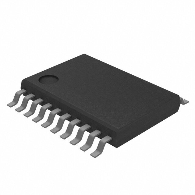
| 描述 | 时钟缓冲器 2 OUTPUT PCIE GEN2 BUFFER |
| 产品分类 | 集成电路 - IC |
| 产品手册 | http://www.idt.com/document/dst/9db102-datasheet |
| 产品图片 |
|
| rohs | 符合RoHS |
| 产品系列 | 时钟和计时器IC,时钟缓冲器,IDT 9DB102BGILF |
| 产品型号 | 9DB102BGILF |
| 产品种类 | 时钟缓冲器 |
| 商标 | IDT |
| 安装风格 | SMD/SMT |
| 封装 | Tube |
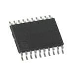
| 封装/箱体 | TSSOP-20 |
| 工厂包装数量 | 74 |
| 最大工作温度 | + 85 C |
| 最大输入频率 | 100 MHz |
| 最大输出频率 | 100 MHz |
| 最小工作温度 | - 40 C |
| 电源电压-最大 | 3.465 V |
| 电源电压-最小 | 3.135 V |
| 电源电流 | 75 mA |
| 系列 | 9DB102 |
| 输入类型 | Clock |
| 输出端数量 | 2 |
| 输出类型 | HCSL |
| 零件号别名 | 9DB102 ICS9DB102BGILF |


- 商务部:美国ITC正式对集成电路等产品启动337调查
- 曝三星4nm工艺存在良率问题 高通将骁龙8 Gen1或转产台积电
- 太阳诱电将投资9.5亿元在常州建新厂生产MLCC 预计2023年完工
- 英特尔发布欧洲新工厂建设计划 深化IDM 2.0 战略
- 台积电先进制程称霸业界 有大客户加持明年业绩稳了
- 达到5530亿美元!SIA预计今年全球半导体销售额将创下新高
- 英特尔拟将自动驾驶子公司Mobileye上市 估值或超500亿美元
- 三星加码芯片和SET,合并消费电子和移动部门,撤换高东真等 CEO
- 三星电子宣布重大人事变动 还合并消费电子和移动部门
- 海关总署:前11个月进口集成电路产品价值2.52万亿元 增长14.8%


PDF Datasheet 数据手册内容提取
DATASHEET Two Output Differential Buffer for PCIe Gen1 & Gen2 ICS9DB102 Description Features/Benefits The ICS9DB102 zero-delay buffer supports PCI Express (cid:129) CLKREQ# pin for outputs 1 and 4/output enable for Express clocking requirements. The ICS9DB102 is driven by a differential Card applications SRC output pair from an ICS CK410/CK505-compliant main (cid:129) PLL or bypass mode/PLL can dejitter incoming clock clock. It attenuates jitter on the input clock and has a selectable (cid:129) Selectable PLL bandwidth/minimizes jitter peaking in PLL Band Width to maximize performance in systems with or downstream PLL’s without Spread-Spectrum clocking. (cid:129) Spread Spectrum Compatible/tracks spreading input clock for low EMI (cid:129) SMBus Interface/unused outputs can be disabled (cid:129) Industrial temperature range available Output Features (cid:127) 2 - 0.7V current mode differential output pairs (HCSL) Key Specifications (cid:129) Cycle-to-cycle jitter < 35ps (cid:129) Output-to-output skew < 25ps Functional Block Diagram CLKREQ0# CLKREQ1# PCIEX0 CLK_INT SPREAD CLK_INC COMPATIBLE PLL PCIEX1 PLL_BW CONTROL SMBDAT LOGIC SMBCLK IREF IDT® Two Output Differential Buffer for PCIe Gen1 & Gen2 852 REV Q 08/27/13 1
ICS9DB102 Two Output Differential Buffer for PCIe Gen1 & Gen2 Pin Configuration Power Groups PLL_BW 1 20 VDDA Pin Number Description CLK_INT 2 19 GNDA VDD GND CLK_INC 3 2 18 IREF 5,9,12,16 6,15 PCI Express Outputs 0 9 6 SMBUS vCLKREQ0# 4 1 17 vCLKREQ1# 20 19 IREF B VDD 5 16 VDD 20 19 Analog VDD & GND for PLL core D GND 6 15 GND 9 PCIEXT0 7 S 14 PCIEXT1 C PCIEXC0 8 13 PCIEXC1 I VDD 9 12 VDD SMBDAT 10 11 SMBCLK Note: Pins preceeded by ' v ' have internal 120K ohm pull down resistors 20-pin SSOP & TSSOP Pin Description PIN # PIN NAME PIN TYPE DESCRIPTION 3.3V input for selecting PLL Band Width 1 PLL_BW IN 0 = low, 1= high 2 CLK_INT IN True Input for differential reference clock. 3 CLK_INC IN Complementary Input for differential reference clock. Output enable for PCI Express output pair 0. 4 vCLKREQ0# IN 0 = enabled, 1 =disabled 5 VDD PWR Power supply, nominal 3.3V 6 GND PWR Ground pin. 7 PCIEXT0 OUT True clock of differential PCI_Express pair. 8 PCIEXC0 OUT Complementary clock of differential PCI_Express pair. 9 VDD PWR Power supply, nominal 3.3V 10 SMBDAT I/O Data pin of SMBUS circuitry, 5V tolerant 11 SMBCLK IN Clock pin of SMBUS circuitry, 5V tolerant 12 VDD PWR Power supply, nominal 3.3V 13 PCIEXC1 OUT Complementary clock of differential PCI_Express pair. 14 PCIEXT1 OUT True clock of differential PCI_Express pair. 15 GND PWR Ground pin. 16 VDD PWR Power supply, nominal 3.3V Output enable for PCI Express output pair 1. 17 vCLKREQ1# IN 0 = enabled, 1 =disabled This pin establishes the reference for the differential current-mode output pairs. It requires a fixed precision resistor to ground. 475ohm is 18 IREF OUT the standard value for 100ohm differential impedance. Other impedances require different values. See data sheet. 19 GNDA PWR Ground pin for the PLL core. 20 VDDA PWR 3.3V power for the PLL core. Note: Pins preceeded by ' v ' have internal 120K ohm pull down resistors IDT® Two Output Differential Buffer for PCIe Gen1 & Gen2 852 REV Q 08/27/13 2
ICS9DB102 Two Output Differential Buffer for PCIe Gen1 & Gen2 Absolute Max Symbol Parameter Min Max Units VDDA 3.3V Core Supply Voltage V + 0.5V V DD VDD 3.3V Output Supply Voltage GND - 0.5 V + 0.5V V DD Ts Storage Temperature -65 150 °C Tcase Case Temperature 115 °C Input ESD protection ESD prot human body model 2000 V Electrical Characteristics - Input/Supply/Common Output Parameters T = Tambient; Supply Voltage V = 3.3 V +/-5% A DD PARAMETER SYMBOL CONDITIONS MIN TYP MAX UNITS NOTES Tambcom Commercial range 0 70 °C 1 Tambient Tambind Industrial range -40 85 °C 1 Input High Voltage V 3.3 V +/-5% 2 V + 0.3 V 1 IH DD Input Low Voltage V 3.3 V +/-5% V - 0.3 0.8 V 1 IL SS Input High Current I V = V -5 5 uA 1 IH IN DD V = 0 V; Inputs with no pull- I IN -5 uA 1 IL1 up resistors Input Low Current V = 0 V; Inputs with pull-up I IN -200 uA 1 IL2 resistors Full Active, C = Full load; 75 100 mA 1 Operating Supply Current I L DD3.3OP all differential pairs tri-stated 27 50 mA 1 Input Frequency3 F V = 3.3 V 99 100 101 MHz 1 i DD Pin Inductance1 L 7 nH 1 pin C Logic Inputs 5 pF 1 Input Capacitance1 IN C Output pin capacitance 4.5 pF 1 OUT From V Power-Up to 1st Clk Stabilization1,2 T DD 1.8 ms 1 STAB clock Modulation Frequency Triangular Modulation 30 33 kHz 1 Spread Spectrum Modulation f Lexmark Modulation 25 45 KHz 1 Frequency MOD DIF start after OE# assertion OE# Latency t DIF stop after OE# 1 3 cycles 1,2 LATOE# deassertion PLL Bandwidth when 400 500 1000 KHz 1 PLL_BW=0 PLL Bandwidth BW PLL Bandwidth when 2 2.5 3 MHz 1 PLL_BW=1 SMBus Voltage V 2.7 5.5 V 1 DD Low-level Output Voltage V @ I 0.4 V 1 OLSMBUS PULLUP Current sinking at V = 0.4 V I SMBus SDATA pin 4 mA 1 OL PULLUP SCLK/SDATA T (Max VIL - 0.15) to (Min VIH + 0.15) 1000 ns 1 Clock/Data Rise Time RI2C SCLK/SDATA T (Min VIH + 0.15) to (Max VIL - 0.15) 300 ns 1 Clock/Data Fall Time FI2C 1Guaranteed by design and characterization, not 100% tested in production. 2Time from deassertion until outputs are >200mV IDT® Two Output Differential Buffer for PCIe Gen1 & Gen2 852 REV Q 08/27/13 3
ICS9DB102 Two Output Differential Buffer for PCIe Gen1 & Gen2 Electrical Characteristics - PCIEX 0.7V Current Mode Differential Pair T = Tambient; V = 3.3 V +/-5%; C =2pF, R =33.2Ω, R =49.9Ω, I = 475Ω A DD L S P REF PARAMETER SYMBOL CONDITIONS MIN TYP MAX UNITS NOTES Current Source Output Zo V = V 3000 Ω 1 Impedance O x Voltage High VHigh Statistical measurement on 660 850 1,3 mV Voltage Low VLow single ended signal using -150 150 1,3 Max Voltage Vovs Measurement on single ended 1150 1,3 mV Min Voltage Vuds signal using absolute value. -300 1,3 Crossing Voltage (abs) Vcross(abs) 250 350 550 mV 1,3 Variation of crossing over all Crossing Voltage (var) d-Vcross 12 140 mV 1,3 edges Long Accuracy ppm see Tperiod min-max values 0 ppm 1,2 100.00MHz nominal 9.9970 10.0030 ns 2 Average period Tperiod 100.00MHz spread 9.9970 10.0533 ns 2 Absolute min period Tabsmin 100.00MHz nominal/spread 9.8720 ns 1,2 Rise Time t V = 0.175V, V = 0.525V 175 700 ps 1 r OL OH Fall Time t V = 0.525V V = 0.175V 175 700 ps 1 f OH OL Rise Time Variation d-t 30 125 ps 1 r Fall Time Variation d-t 30 125 ps 1 f t PLL Mode. 0 150 ps 1 Input to Output Delay pd t Bypass mode 3.7 4.2 ns 1 pdbyp Measurement from differential Duty Cycle d 45 55 % 1 t3 wavefrom Output-to-Output Skew t V = 50% 25 ps 1 sk3 T PLL mode. Measurement from t 35 ps 1 Jitter, Cycle to cycle jcyc-cyc differential wavefrom t Additve Jitter in Bypass Mode 30 ps 1 jcyc-cycbyp 1Guaranteed by design, not 100% tested in production. . 2 The 9DB102 does not add a ppm error to the input clock 3I = V /(3xR ). For R = 475Ω (1%), I = 2.32mA. I = 6 x I and V = 0.7V @ Z =50Ω. REF DD R R REF OH REF OH O IDT® Two Output Differential Buffer for PCIe Gen1 & Gen2 852 REV Q 08/27/13 4
ICS9DB102 Two Output Differential Buffer for PCIe Gen1 & Gen2 Electrical Characteristics - PLL Parameters T = Tambient; Supply Voltage V = 3.3 V +/-5% A DD Group Parameter Description Min Typ Max Units Notes PLL Jitter Peaking j (PLL_BW = 1) 0 1 2.5 dB 1,4 peak-hibw PLL Jitter Peaking j (PLL_BW = 0) 0 1 2 dB 1,4 peak-lobw PLL Bandwidth pll (PLL_BW = 1) 2 2.5 3 MHz 1,5 HIBW PLL Bandwidth pll (PLL_BW = 0) 0.4 0.5 1 MHz 1,5 LOBW PCIe Gen 1 phase jitter 40 108 ps 1,2,3 (1.5 - 22 MHz) PCIe Gen 2 jitter (8-16 MHz, 5-16 MHz) Hi-Band >1.5MHz 2.7 3.1 ps rms 1,2,3 (PLL_BW=1) Jitter, Phase t jphasePLL PCIe Gen 2 jitter (8-16 MHz, 5-16 MHz) Hi-Band >1.5MHz 2.2 3.1 ps rms 1,2,3 (PLL_BW=0) PCIe Gen 2 jitter 1.3 3 ps rms 1,2,3 (8-16 MHz, 5-16 MHz) Lo-Band <1.5MHz NOTES: 1. Guaranteed by design and characterization, not 100% tested in production. 2. See http://www.pcisig.com for complete specs 3. Device driven by 932S421BGLF or equivalent 4. Measured as maximum pass band gain. At frequencies within the loop BW, highest point of magnification is called PLL jitter peaking. 5. Measured at 3 db down or half power point. IDT® Two Output Differential Buffer for PCIe Gen1 & Gen2 852 REV Q 08/27/13 5
ICS9DB102 Two Output Differential Buffer for PCIe Gen1 & Gen2 SRC Reference Clock Common Recommendations for Differential Routing Dimension or Value Unit Figure L1 length, route as non-coupled 50ohm trace 0.5 max inch 1 L2 length, route as non-coupled 50ohm trace 0.2 max inch 1 L3 length, route as non-coupled 50ohm trace 0.2 max inch 1 Rs 33 ohm 1 Rt 49.9 ohm 1 Down Device Differential Routing L4 length, route as coupled microstrip 100ohm differential trace 2 min to 16 max inch 1 L4 length, route as coupled stripline 100ohm differential trace 1.8 min to 14.4 max inch 1 Differential Routing to PCI Express Connector L4 length, route as coupled microstrip 100ohm differential trace 0.25 to 14 max inch 2 L4 length, route as coupled stripline 100ohm differential trace 0.225 min to 12.6 max inch 2 Figure 1: Down Device Routing L1 L2 Rs L4 L4' L1' L2' Rs HCSL Output Buffer Rt Rt PCI Express Down Device REF_CLK Input L3' L3 Figure 2: PCI Express Connector Routing L1 L2 Rs L4 L4' L1' L2' Rs HCSL Output Buffer Rt Rt PCI Express Add-in Board REF_CLK Input L3' L3 IDT® Two Output Differential Buffer for PCIe Gen1 & Gen2 852 REV Q 08/27/13 6
ICS9DB102 Two Output Differential Buffer for PCIe Gen1 & Gen2 Alternative Termination for LVDS and other Common Differential Signals (figure 3) Vdiff Vp-p Vcm R1 R2 R3 R4 Note 0.45v 0.22v 1.08 33 150 100 100 0.58 0.28 0.6 33 78.7 137 100 0.80 0.40 0.6 33 78.7 none 100 ICS874003i-02 input compatible 0.60 0.3 1.2 33 174 140 100 Standard LVDS R1a = R1b = R1 R2a = R2b = R2 Figure 3 L1 L2 R3 R4 R1a L4 L4' L1' L2' R1b HCSL Output Buffer R2a R2b Down Device REF_CLK Input L3' L3 Cable Connected AC Coupled Application (figure 4) Component Value Note R5a, R5b 8.2K 5% R6a, R6b 1K 5% Cc 0.1 µF Vcm 0.350 volts Figure 4 3.3 Volts R5a R5b Cc L4 L4' Cc R6a R6b PCIe Device REF_CLK Input IDT® Two Output Differential Buffer for PCIe Gen1 & Gen2 852 REV Q 08/27/13 7
ICS9DB102 Two Output Differential Buffer for PCIe Gen1 & Gen2 General SMBus serial interface information for the ICS9DB102 How to Write: How to Read: • Controller (host) sends a start bit. (cid:129) Controller (host) will send start bit. (cid:129) Controller (host) sends the write address D4 (cid:129) Controller (host) sends the write address D4 (h) (h) (cid:129) IDT clock will acknowledge (cid:129) IDT clock will acknowledge (cid:129) Controller (host) sends the begining byte location = N (cid:129) Controller (host) sends the begining byte (cid:129) IDT clock will acknowledge location = N (cid:129) Controller (host) sends the data byte count = X (cid:129) IDT clock will acknowledge (cid:129) IDT clock will acknowledge (cid:129) Controller (host) will send a separate start bit. (cid:129) Controller (host) starts sending Byte N through (cid:129) Controller (host) sends the read address D5 (h) Byte N + X -1 (cid:129) IDT clock will acknowledge (cid:129) IDT clock will acknowledge each byte one at a time (cid:129) IDT clock will send the data byte count = X (cid:129) Controller (host) sends a Stop bit (cid:129) IDT clock sends Byte N + X -1 (cid:129) IDT clock sends Byte 0 through byte X (if X (h) was written to byte 8). (cid:129) Controller (host) will need to acknowledge each byte (cid:129) Controllor (host) will send a not acknowledge bit (cid:129) Controller (host) will send a stop bit Index Block Write Operation Index Block Read Operation Controller (Host) IDT (Slave/Receiver) Controller (Host) IDT (Slave/Receiver) T starT bit T starT bit Slave Address D4 Slave Address D4 (h) (h) WR WRite WR WRite ACK ACK Beginning Byte = N Beginning Byte = N ACK ACK Data Byte Count = X RT Repeat starT ACK Slave Address D5 (h) Beginning Byte N RD ReaD ACK ACK e yt B Data Byte Count = X X ACK Beginning Byte N Byte N + X - 1 ACK ACK e P stoP bit yt B X Byte N + X - 1 N Not acknowledge P stoP bit IDT® Two Output Differential Buffer for PCIe Gen1 & Gen2 852 REV Q 08/27/13 8
ICS9DB102 Two Output Differential Buffer for PCIe Gen1 & Gen2 SMBus Table: Device Control Register, READ/WRITE ADDRESS (D4/D5) Byte 0 Pin # Name Control Function Type 0 1 PWD Functions Functions Enables SMBus controlled by Bit 7 - SW_EN RW controlled by 1 Control SMBus device pins registers Bit 6 - RESERVED RW - X Bit 5 - RESERVED RW - X Bit 4 - RESERVED RW - X Bit 3 - RESERVED RW - X Bit 2 - RESERVED RW - X Selects PLL Bit 1 - PLL BW #adjust RW Low BW High BW 1 Bandwidth Bypasses PLL for PLL bypassed PLL enabled Bit 0 - PLL Enable RW 1 board test (fan out mode) (ZDB mode) SMBus Table: Output Enable Register Byte 1 Pin # Name Control Function Type 0 1 PWD Bit 7 - RESERVED RW - X Bit 6 - RESERVED RW - X Bit 5 - RESERVED RW - X Bit 4 - RESERVED RW - X Bit 3 - RESERVED RW - X Bit 2 - RESERVED RW - X Bit 1 - RESERVED RW - X Bit 0 - RESERVED RW - X SMBus Table: Function Select Register Byte 2 Pin # Name Control Function Type 0 1 PWD Bit 7 RESERVED RW - X Bit 6 RESERVED RW - X Bit 5 - RESERVED RW - X Bit 4 - RESERVED RW - X Bit 3 - RESERVED RW - X Bit 2 - RESERVED RW - X Bit 1 - RESERVED RW - X Bit 0 - RESERVED RW - X SMBus Table: Vendor & Revision ID Register Byte 3 Pin # Name Control Function Type 0 1 PWD Bit 7 - RID3 R - - 0 Bit 6 - RID2 R - - 0 REVISION ID Bit 5 - RID1 R - - 0 Bit 4 - RID0 R - - 1 Bit 3 - VID3 R - - 0 Bit 2 - VID2 R - - 0 VENDOR ID Bit 1 - VID1 R - - 0 Bit 0 - VID0 R - - 1 IDT® Two Output Differential Buffer for PCIe Gen1 & Gen2 852 REV Q 08/27/13 9
ICS9DB102 Two Output Differential Buffer for PCIe Gen1 & Gen2 SMBus Table: DEVICE ID Byte 4 Pin # Name Control Function Type 0 1 PWD Bit 7 - R - 0 Bit 6 - R - 0 Bit 5 - R - 0 Bit 4 - Device ID R - 0 Bit 3 - = 06 Hex R - 0 Bit 2 - R - 1 Bit 1 - R - 1 Bit 0 - R - 0 SMBus Table: Byte Count Register Control Byte 5 Pin # Name Type 0 1 PWD Function Bit 7 - BC7 RW - - 0 Bit 6 - BC6 Writing to this RW - - 0 Bit 5 - BC5 register will RW - - 0 Bit 4 - BC4 configure how RW - - 0 Bit 3 - BC3 many bytes will be RW - - 0 Bit 2 - BC2 read back, default RW - - 1 Bit 1 - BC1 is 06= 6 bytes. RW - - 1 Bit 0 - BC0 RW - - 0 IDT® Two Output Differential Buffer for PCIe Gen1 & Gen2 852 REV Q 08/27/13 10
ICS9DB102 Two Output Differential Buffer for PCIe Gen1 & Gen2 20-Pin SSOP Package Drawing and Dimensions 20-Lead, 150 mil SSOP (QSOP) In Millimeters In Inches SYMBOL COMMON DIMENSIONS COMMON DIMENSIONS MIN MAX MIN MAX A 1.35 1.75 .053 .069 A1 0.10 0.25 .004 .010 A2 -- 1.50 -- .059 b 0.20 0.30 .008 .012 c 0.18 0.25 .007 .010 D 8.55 8.75 .337 .344 E 5.80 6.20 .228 .244 E1 3.80 4.00 .150 .157 e 0.635 BASIC 0.025 BASIC L 0.40 1.27 .016 .050 N 20 20 a 0° 8° 0° 8° ZD 1.47 .058 IDT® Two Output Differential Buffer for PCIe Gen1 & Gen2 852 REV Q 08/27/13 11
ICS9DB102 Two Output Differential Buffer for PCIe Gen1 & Gen2 20-Pin TSSOP Package Drawing and Dimensions 20-Lead, 4.40 mm. Body, 0.65 mm. Pitch TSSOP c N (173 mil) (25.6 mil) In Millimeters In Inches SYMBOL COMMON DIMENSIONS COMMON DIMENSIONS L MIN MAX MIN MAX A -- 1.20 -- .047 E1 E IINNDDEEXX A1 0.05 0.15 .002 .006 AARREEAA A2 0.80 1.05 .032 .041 b 0.19 0.30 .007 .012 c 0.09 0.20 .0035 .008 D 6.40 6.60 .252 .260 11 22 E 6.40 BASIC 0.252 BASIC α E1 4.30 4.50 .169 .177 D e 0.65 BASIC 0.0256 BASIC L 0.45 0.75 .018 .030 N 20 20 a 0° 8° 0° 8° A A2 aaa -- 0.10 -- .004 A1 --CC-- Reference Doc.: JEDEC Publication 95, MO-153 e SSEEAATTIINNGG 10-0035 b PPLLAANNEE aaa C Ordering Information Part / Order Number Shipping Packaging Package Temperature 9DB102BFLF Tubes 20-pin SSOP 0 to +70°C 9DB102BFLFT Tape and Reel 20-pin SSOP 0 to +70°C 9DB102BFILF Tubes 20-pin SSOP -40 to +85°C 9DB102BFILFT Tape and Reel 20-pin SSOP -40 to +85°C 9DB102BGLF Tubes 20-pin TSSOP 0 to +70°C 9DB102BGLFT Tape and Reel 20-pin TSSOP 0 to +70°C 9DB102BGILF Tubes 20-pin TSSOP -40 to +85°C 9DB102BGILFT Tape and Reel 20-pin TSSOP -40 to +85°C "LF" after the package code are the Pb-Free configuration and are RoHS compliant. "B" is the device revision designator (will not correlate to the datasheet revision). IDT® Two Output Differential Buffer for PCIe Gen1 & Gen2 852 REV Q 08/27/13 12
ICS9DB102 Two Output Differential Buffer for PCIe Gen1 & Gen2 Revision History Rev. Originator Issue Date Description Page # 1. Added Phase Noise Parameters, Updated input to output delay values. 2. PLL BW moved to PLL parameters table. F 8/6/2007 3. Added terminations tables. Various G 12/14/2007 Updated General SMBus Interface Information. 8 H 10/29/2008 Corrected "HCSL" typos. 1, 6, 7 1. Added I-temp electricals 2. Changed datasheet title J 1/15/2010 Various 3. Updated Input Frequency parameter 4. Updated ordering information K RW 4/1/2010 Updated ordering info for Rev B L DC 9/28/2010 Updated package dimension tables 11, 12 M RDW 1/27/2011 Updated Termination Figure 4. 7 Changed pulldown indicator on CLKREQ# pins to correct pin description of N RDW 4/20/2011 those pins. P AT 5/24/2012 Added OE# Latency spec to Common Input/Output Parameters table 3 Q J. Chao 8/27/2013 Updated PLL Bandwidth specs per latest characterization data, 3 Innovate with IDT and accelerate your future networks. Contact: www.IDT.com For Sales For Tech Support 800-345-7015 408-284-6578 408-284-8200 pcclockhelp@idt.com Fax: 408-284-2775 Corporate Headquarters Integrated Device Technology, Inc. 6024 Silver Creek Valley Road San Jose, CA 95138 United States 800 345 7015 +408 284 8200 (outside U.S.) © 2013 Integrated Device Technology, Inc. All rights reserved. Product specifications subject to change without notice. IDT, ICS, and the IDT logo are trademarks of Integrated Device Technology, Inc. Accelerated Thinking is a service mark of Integrated Device Technology, Inc. All other brands, product names and marks are or may be trademarks or registered trademarks used to identify products or services of their respective owners. Printed in USA
Mouser Electronics Authorized Distributor Click to View Pricing, Inventory, Delivery & Lifecycle Information: I DT (Integrated Device Technology): 9DB102BGLFT 9DB102BGILF 9DB102BFLF 9DB102BGLF 9DB102BFLFT 9DB102BGILFT