ICGOO在线商城 > 集成电路(IC) > 时钟/计时 - 专用 > CY2304NZZXI-1
 Datasheet下载
- 型号: CY2304NZZXI-1
- 制造商: Cypress Semiconductor
- 库位|库存: xxxx|xxxx
- 要求:
| 数量阶梯 | 香港交货 | 国内含税 |
| +xxxx | $xxxx | ¥xxxx |
查看当月历史价格
查看今年历史价格
CY2304NZZXI-1产品简介:
ICGOO电子元器件商城为您提供CY2304NZZXI-1由Cypress Semiconductor设计生产,在icgoo商城现货销售,并且可以通过原厂、代理商等渠道进行代购。 CY2304NZZXI-1价格参考¥53.90-¥53.90。Cypress SemiconductorCY2304NZZXI-1封装/规格:时钟/计时 - 专用, 。您可以下载CY2304NZZXI-1参考资料、Datasheet数据手册功能说明书,资料中有CY2304NZZXI-1 详细功能的应用电路图电压和使用方法及教程。
Cypress Semiconductor Corp. 的 CY2304NZZXI-1 是一款专用时钟/计时芯片,主要应用于需要高精度时钟信号的电子设备中。以下是该型号的应用场景:

 1. 通信设备
   在通信系统中,精确的时钟信号对于确保数据传输的同步至关重要。CY2304NZZXI-1 可用于路由器、交换机、基站等设备中,提供稳定的时钟源,确保数据包的准确传输和接收。它能够支持多种通信协议,如以太网、光纤通道等,确保系统的稳定性和可靠性。

 2. 网络基础设施
   网络基础设施设备(如服务器、存储设备)需要高精度的时钟来保持系统的同步性。CY2304NZZXI-1 可以为这些设备提供稳定的时钟信号,确保数据处理和传输的准确性。此外,它还可以用于时间敏感网络(TSN),确保不同设备之间的时钟同步。

 3. 工业自动化
   在工业自动化领域,精确的时间控制对于生产线的高效运作至关重要。CY2304NZZXI-1 可用于工业控制器、PLC(可编程逻辑控制器)等设备中,提供高精度的时钟信号,确保各个设备之间的协调工作。它还可以用于实时控制系统,确保任务按时执行。

 4. 消费电子产品
   某些高端消费电子产品(如智能电视、音响设备)对音视频同步有较高要求。CY2304NZZXI-1 可以为这些设备提供稳定的时钟信号,确保音视频的同步播放,提升用户体验。此外,它还可以用于智能家居设备中,确保各个设备之间的时间同步。

 5. 测试与测量设备
   测试与测量设备(如示波器、频谱分析仪)需要高精度的时钟信号来确保测量结果的准确性。CY2304NZZXI-1 可以为这些设备提供稳定的时钟源,确保测量的精度和可靠性。它还可以用于校准设备,确保其长期稳定性。

 6. 汽车电子
   在汽车电子系统中,尤其是涉及自动驾驶和高级驾驶辅助系统(ADAS)的设备,精确的时间控制非常重要。CY2304NZZXI-1 可以为这些系统提供高精度的时钟信号,确保传感器数据的同步处理,提升系统的安全性和可靠性。

总之,CY2304NZZXI-1 适用于需要高精度时钟信号的各种应用场景,尤其是在通信、网络、工业自动化等领域,能够为系统提供稳定可靠的时钟源,确保设备的正常运行。
| 参数 | 数值 |
| 产品目录 | 集成电路 (IC)半导体 |
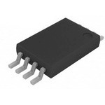
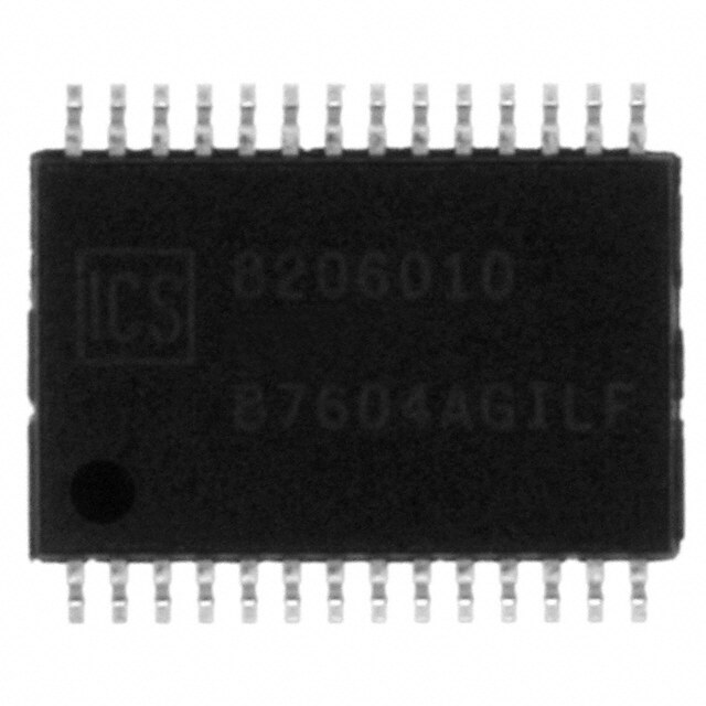
| 描述 | IC CLK ZDB 4OUT 140MHZ 8TSSOP时钟缓冲器 3.3V 133MHz IND |
| 产品分类 | |
| 品牌 | Cypress Semiconductor Corp |
| 产品手册 | |
| 产品图片 |
|
| rohs | 符合RoHS无铅 / 符合限制有害物质指令(RoHS)规范要求 |
| 产品系列 | 时钟和计时器IC,时钟缓冲器,Cypress Semiconductor CY2304NZZXI-1- |
| 数据手册 | http://www.cypress.com/?docID=48468 |
| 产品型号 | CY2304NZZXI-1 |
| PCN组件/产地 | http://www.cypress.com/?docID=44762 |
| PLL | 无 |
| 主要用途 | PCI Express(PCIe) |
| 产品目录页面 | |
| 产品种类 | 时钟缓冲器 |
| 传播延迟—最大值 | 5 ns |
| 供应商器件封装 | 8-TSSOP |
| 其它名称 | 428-2191 |
| 包装 | 管件 |
| 商标 | Cypress Semiconductor |
| 安装类型 | 表面贴装 |
| 安装风格 | SMD/SMT |
| 封装 | Tube |
| 封装/外壳 | 8-TSSOP(0.173",4.40mm 宽) |
| 封装/箱体 | TSSOP-8 |
| 工作温度 | -40°C ~ 85°C |
| 工厂包装数量 | 162 |
| 差分-输入:输出 | 无/无 |
| 最大工作温度 | + 85 C |
| 最大输入频率 | 140 MHz |
| 最小工作温度 | - 40 C |
| 标准包装 | 162 |
| 比率-输入:输出 | 1:4 |
| 电压-电源 | 3 V ~ 3.6 V |
| 电源电压-最大 | 3.6 V |
| 电源电压-最小 | 3 V |
| 电路数 | 1 |
| 系列 | CY2304NZZXI |
| 输入 | LVCMOS,LVTTL |
| 输出 | LVCMOS |
| 输出端数量 | 4 |
| 频率-最大值 | 140MHz |


- 商务部:美国ITC正式对集成电路等产品启动337调查
- 曝三星4nm工艺存在良率问题 高通将骁龙8 Gen1或转产台积电
- 太阳诱电将投资9.5亿元在常州建新厂生产MLCC 预计2023年完工
- 英特尔发布欧洲新工厂建设计划 深化IDM 2.0 战略
- 台积电先进制程称霸业界 有大客户加持明年业绩稳了
- 达到5530亿美元!SIA预计今年全球半导体销售额将创下新高
- 英特尔拟将自动驾驶子公司Mobileye上市 估值或超500亿美元
- 三星加码芯片和SET,合并消费电子和移动部门,撤换高东真等 CEO
- 三星电子宣布重大人事变动 还合并消费电子和移动部门
- 海关总署:前11个月进口集成电路产品价值2.52万亿元 增长14.8%


PDF Datasheet 数据手册内容提取
CY2304NZ Four Output PCI-X and General Purpose Buffer Four Output PCI-X and General Purpose Buffer Features Functional Description ■One input to four output buffer/driver The CY2304NZ is a low-cost buffer designed to distribute high-speed clocks for PCI-X and other applications. The device ■General-purpose or PCI-X clock buffer operates at 3.3 V and outputs can run up to 140 MHz. ■Buffers all frequencies from DC to 140 MHz For a complete list of related documentation, click here. ■Output-to-output skew less than 100 ps Function Table ■Space-saving 8-pin TSSOP package Inputs Outputs ■3.3 V operation BUF_IN OE Output [1:4] ■60 ps typical output-output skew L L L H L L L H L H H H Block Diagram Logic OE Control BUF_IN OUTPUT1 OUTPUT2 OUTPUT3 OUTPUT4 Pin Configuration 8-pin TSSOP Top View BUF_IN 1 8 OUTPUT4 OE 2 7 OUTPUT3 OUTPUT1 3 6 VDD GND 4 5 OUTPUT2 Pin Description For CY2304NZ Signal Pin Description V 6 3.3 V voltage supply DD GND 4 Ground BUF_IN 1 Input clock OUTPUT [1:4] 3, 5, 7, 8 Outputs OE 2 Input pin for output enable, active HIGH. CypressSemiconductorCorporation • 198 Champion Court • SanJose, CA 95134-1709 • 408-943-2600 Document Number: 38-07099 Rev. *K Revised May 4, 2016
CY2304NZ Maximum Ratings Storage Temperature ...............................–65 °C to +150 °C Max. Soldering Temperature (10 sec.) ......................260 °C Supply Voltage to Ground Potential ....–0.5 V to V + 0.5 V DD Junction Temperature ................................................150 °C DC Input Voltage ................................–0.5 V to V + 0.5 V DD Operating Conditions Parameter Description Min Max Unit V Supply Voltage 3.0 3.6 V DD T Operating Temperature (Ambient Temperature) –40 85 °C A C Load Capacitance – 25 pF L C Input Capacitance – 7 pF IN BUF_IN, Operating Frequency DC 140 MHz OUTPUT [1:4] t [1] Power-up time for all VDD’s to reach minimum specified voltage (power ramps must 0.05 50 ms PU be monotonic) Electrical Characteristics Parameter Description Test Conditions Min Max Unit V Input LOW Voltage [2] – 0.8 V IL V Input HIGH Voltage [2] 2.0 – V IH I Input LOW Current V = 0 V –5 5 A IL IN I Input HIGH Current V = V –5 5 A IH IN DD V Output LOW Voltage [3] I = 24 mA – 0.8 V OL OL I = 12 mA – 0.55 V OL V Output HIGH Voltage [3] I = –24 mA 2.0 – V OH OH I = –12 mA 2.4 – V OH I Supply Current Unloaded outputs at 66.66 MHz – 25 mA DD Thermal Resistance Parameter [4] Description Test Conditions 8-pin TSSOP Unit θ Thermal resistance Test conditions follow standard test methods and 165 °C/W JA (junction to ambient) procedures for measuring thermal impedance, in accordance with EIA/JESD51. θ Thermal resistance 33 °C/W JC (junction to case) Notes 1. This operating condition guarantees skew and propagation delay. 2. BUF_IN input has a threshold voltage of VDD/2. 3. Parameter is guaranteed by design and characterization. It is not 100% tested in production. 4. These parameters are guaranteed by design and are not tested. Document Number: 38-07099 Rev. *K Page 2 of 8
CY2304NZ Switching Characteristics For Commercial and Industrial Temperature Devices which are characterized over the frequency range of 1 MHz to 140 MHz. Parameter [5] Name Description Min Typ Max Unit Duty Cycle [6] = t t Measured at 1.5 V 40.0 50.0 60.0 % 2 1 t Rise Time [6] Measured between 0.8 V and 2.0 V – – 1.50 ns 3 t Fall Time [6] Measured between 0.8 V and 2.0 V – – 1.50 ns 4 t Output to Output Skew [6] All outputs equally loaded – 60 100 ps 5 t Propagation Delay, Measured at V /2 2.5 3.5 5 ns 6 DD BUF_IN Rising Edge to OUTPUT Rising Edge [6] Switching Waveforms Figure 1. Duty Cycle Timing t1 t2 1.5 V 1.5 V 1.5 V Figure 2. All Outputs Rise/Fall Time 2.0 V 2.0 V 3.3 V OUTPUT 0.8 V 0.8 V 0 V t3 t4 Figure 3. Output-Output Skew 1.5 V OUTPUT 1.5 V OUTPUT t5 Figure 4. Input-Output Propagation Delay V /2 INPUT DD V /2 OUTPUT DD t6 Notes 5. All parameters specified with loaded outputs. 6. Parameter is guaranteed by design and characterization. It is not 100% tested in production. Document Number: 38-07099 Rev. *K Page 3 of 8
CY2304NZ Ordering Information Ordering Code Package Type Operating Range Standard CY2304NZZI-1 8-pin TSSOP Industrial, –40 °C to 85 °C CY2304NZZI-1T 8-pin TSSOP – Tape and Reel Industrial, –40 °C to 85 °C Pb-free CY2304NZZXC-1 8-pin TSSOP Commercial, 0 °C to 70 °C CY2304NZZXC-1T 8-pin TSSOP – Tape and Reel Commercial, 0 °C to 70 °C CY2304NZZXI-1 8-pin TSSOP Industrial, –40 °C to 85 °C CY2304NZZXI-1T 8-pin TSSOP – Tape and Reel Industrial, –40 °C to 85 °C Ordering Code Definitions CY 2304NZ Z X X - X X X = blank or T blank = Tube; T = Tape and Reel X = 1 or 2 Temperature Range: X = C or I C = Commercial; I = Industrial X = Pb-free Package Type: Z = 8-pin TSSOP Base Device Part Number Company ID: CY = Cypress Document Number: 38-07099 Rev. *K Page 4 of 8
CY2304NZ Package Diagram Figure 5. 8-pin TSSOP (4.40 mm Body) Z08.173/ZZ08.173 Package Outline, 51-85093 51-85093 *E Document Number: 38-07099 Rev. *K Page 5 of 8
CY2304NZ Acronyms Document Conventions Acronym Description Units of Measure PCI Peripheral Component Interconnect Symbol Unit of Measure TSSOP Thin-Shrink Small Outline Package °C degree Celsius Hz hertz MHz megahertz µA microampere mA milliampere ms millisecond mV millivolt ns nanosecond ohm % percent pF picofarad ps picosecond V volt W watt Document Number: 38-07099 Rev. *K Page 6 of 8
CY2304NZ Document History Page Document Title: CY2304NZ, Four Output PCI-X and General Purpose Buffer Document Number: 38-07099 Orig. of Rev. ECN No. Issue Date Description of Change Change ** 111420 02/12/02 IKA New data sheet. *A 118610 09/25/02 HWT Updated Ordering Information: Added Industrial Temperature Range in the Ordering Information. *B 121820 12/14/02 RBI Updated Operating Conditions: Added t parameter and its details. PU *C 291098 See ECN RGL Updated Switching Characteristics: Specified typical value for “Output to Output Skew” parameter. Updated Ordering Information: Added Lead-free Devices. *D 2904623 04/05/10 CXQ Updated Ordering Information (Removed inactive parts). Updated Package Diagram. *E 3163624 02/05/2011 CXQ Updated Maximum Ratings (Removed reference to “Except REF” and “REF” for DC Input Voltage spec). Added Ordering Code Definitions. Updated Package Diagram. Added Acronyms and Units of Measure. Updated to new template. *F 3931498 04/08/2013 PURU Updated Maximum Ratings: Removed “Static Discharge Voltage” and its related information. Updated Package Diagram: spec 51-85093 – Changed revision from *C to *D. *G 4103402 08/23/2013 MNSB Updated Operating Conditions: Added Note 1 and referred the same note in t parameter. PU Updated to new template. *H 4312848 03/18/2014 CINM No technical updates. Completing Sunset Review. *I 4578443 11/25/2014 AJU Updated Functional Description: Added “For a complete list of related documentation, click here.” at the end. Updated Package Diagram: spec 51-85093 – Changed revision from *D to *E. *J 4756553 05/06/2015 TAVA Updated Switching Characteristics: Replaced “For Commercial and Industrial Temperature Devices” with “For Commercial and Industrial Temperature Devices which are characterized over the frequency range of 1 MHz to 140 MHz.” for characterization. *K 5258800 05/04/2016 PSR Added Thermal Resistance. Updated to new template. Document Number: 38-07099 Rev. *K Page 7 of 8
CY2304NZ Sales, Solutions, and Legal Information Worldwide Sales and Design Support Cypress maintains a worldwide network of offices, solution centers, manufacturer’s representatives, and distributors. To find the office closest to you, visit us at Cypress Locations. Products PSoC®Solutions ARM® Cortex® Microcontrollers cypress.com/arm PSoC 1 | PSoC 3 | PSoC 4 | PSoC 5LP Automotive cypress.com/automotive Cypress Developer Community Clocks & Buffers cypress.com/clocks Forums | Projects | Video | Blogs | Training | Components Interface cypress.com/interface Technical Support Lighting & Power Control cypress.com/powerpsoc cypress.com/support Memory cypress.com/memory PSoC cypress.com/psoc Touch Sensing cypress.com/touch USB Controllers cypress.com/usb Wireless/RF cypress.com/wireless © Cypress Semiconductor Corporation, 2002-2016. This document is the property of Cypress Semiconductor Corporation and its subsidiaries, including Spansion LLC ("Cypress"). This document, including any software or firmware included or referenced in this document ("Software"), is owned by Cypress under the intellectual property laws and treaties of the United States and other countries worldwide. Cypress reserves all rights under such laws and treaties and does not, except as specifically stated in this paragraph, grant any license under its patents, copyrights, trademarks, or other intellectual property rights. If the Software is not accompanied by a license agreement and you do not otherwise have a written agreement with Cypress governing the use of the Software, then Cypress hereby grants you a personal, non-exclusive, nontransferable license (without the right to sublicense) (1) under its copyright rights in the Software (a) for Software provided in source code form, to modify and reproduce the Software solely for use with Cypress hardware products, only internally within your organization, and (b) to distribute the Software in binary code form externally to end users (either directly or indirectly through resellers and distributors), solely for use on Cypress hardware product units, and (2) under those claims of Cypress's patents that are infringed by the Software (as provided by Cypress, unmodified) to make, use, distribute, and import the Software solely for use with Cypress hardware products. Any other use, reproduction, modification, translation, or compilation of the Software is prohibited. TO THE EXTENT PERMITTED BY APPLICABLE LAW, CYPRESS MAKES NO WARRANTY OF ANY KIND, EXPRESS OR IMPLIED, WITH REGARD TO THIS DOCUMENT OR ANY SOFTWARE OR ACCOMPANYING HARDWARE, INCLUDING, BUT NOT LIMITED TO, THE IMPLIED WARRANTIES OF MERCHANTABILITY AND FITNESS FOR A PARTICULAR PURPOSE. To the extent permitted by applicable law, Cypress reserves the right to make changes to this document without further notice. Cypress does not assume any liability arising out of the application or use of any product or circuit described in this document. Any information provided in this document, including any sample design information or programming code, is provided only for reference purposes. It is the responsibility of the user of this document to properly design, program, and test the functionality and safety of any application made of this information and any resulting product. Cypress products are not designed, intended, or authorized for use as critical components in systems designed or intended for the operation of weapons, weapons systems, nuclear installations, life-support devices or systems, other medical devices or systems (including resuscitation equipment and surgical implants), pollution control or hazardous substances management, or other uses where the failure of the device or system could cause personal injury, death, or property damage ("Unintended Uses"). A critical component is any component of a device or system whose failure to perform can be reasonably expected to cause the failure of the device or system, or to affect its safety or effectiveness. Cypress is not liable, in whole or in part, and you shall and hereby do release Cypress from any claim, damage, or other liability arising from or related to all Unintended Uses of Cypress products. You shall indemnify and hold Cypress harmless from and against all claims, costs, damages, and other liabilities, including claims for personal injury or death, arising from or related to any Unintended Uses of Cypress products. Cypress, the Cypress logo, Spansion, the Spansion logo, and combinations thereof, PSoC, CapSense, EZ-USB, F-RAM, and Traveo are trademarks or registered trademarks of Cypress in the United States and other countries. For a more complete list of Cypress trademarks, visit cypress.com. Other names and brands may be claimed as property of their respective owners. Document Number: 38-07099 Rev. *K Revised May 4, 2016 Page 8 of 8