
 Datasheet下载
- 型号: 93LC56B-I/MS
- 制造商: Microchip
- 库位|库存: xxxx|xxxx
- 要求:
| 数量阶梯 | 香港交货 | 国内含税 |
| +xxxx | $xxxx | ¥xxxx |
查看当月历史价格
查看今年历史价格
93LC56B-I/MS产品简介:
ICGOO电子元器件商城为您提供93LC56B-I/MS由Microchip设计生产,在icgoo商城现货销售,并且可以通过原厂、代理商等渠道进行代购。 93LC56B-I/MS价格参考。Microchip93LC56B-I/MS封装/规格:存储器, EEPROM 存储器 IC 2Kb (128 x 16) SPI 2MHz 8-MSOP。您可以下载93LC56B-I/MS参考资料、Datasheet数据手册功能说明书,资料中有93LC56B-I/MS 详细功能的应用电路图电压和使用方法及教程。
Microchip Technology的93LC56B-I/MS是一款串行EEPROM(电可擦除可编程只读存储器),主要用于数据存储和配置参数保存。其应用场景广泛,特别适合需要可靠、低功耗、小封装且具备串行接口的嵌入式系统。以下是该型号的具体应用场景:

1. 工业自动化:在工业控制系统中,93LC56B-I/MS可用于保存设备配置、校准数据和运行参数。例如,PLC(可编程逻辑控制器)可以使用这款EEPROM来存储程序代码和设置,确保断电后数据不会丢失。

2. 消费电子:在家电和消费类电子产品中,如智能电视、音响设备等,该芯片用于存储用户偏好设置、音量调节、频道列表等信息。它还可以用于固件升级,确保设备在更新过程中数据的安全性和完整性。

3. 通信设备:在网络路由器、调制解调器和其他通信设备中,93LC56B-I/MS可用于保存MAC地址、IP配置和其他网络参数。它还支持远程配置和维护,确保设备在网络中的稳定运行。

4. 汽车电子:在汽车电子系统中,如车载娱乐系统、仪表盘和发动机控制单元,该芯片用于存储车辆配置、诊断数据和用户设置。它具有良好的抗干扰能力和宽温度范围,适用于恶劣的工作环境。

5. 医疗设备:在医疗仪器中,如血糖仪、心率监测器等,93LC56B-I/MS可用于保存患者的测量数据和设备校准信息。它的小封装和低功耗特性使其非常适合便携式医疗设备。

6. 物联网(IoT):在物联网设备中,如传感器节点和智能网关,该芯片用于存储设备标识、连接参数和历史数据。它支持SPI接口,便于与主控MCU进行高效通信。

总之,93LC56B-I/MS以其高可靠性、低功耗和灵活的应用特性,在多个领域提供了可靠的存储解决方案,特别是在需要长期保存关键数据和配置信息的场景中表现出色。
| 参数 | 数值 |
| 产品目录 | 集成电路 (IC)半导体 |
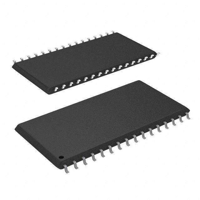
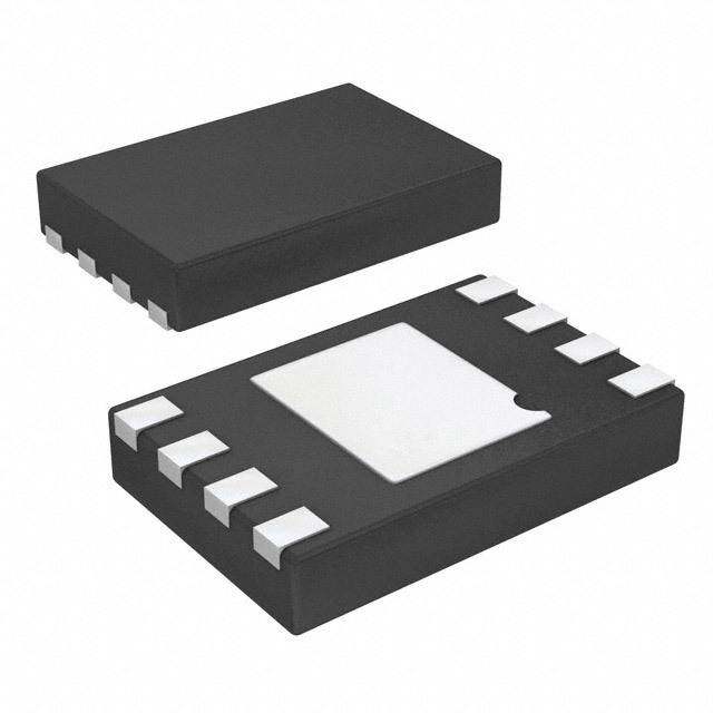
| 描述 | IC EEPROM 2KBIT 2MHZ 8MSOP电可擦除可编程只读存储器 128x16 |
| 产品分类 | |
| 品牌 | Microchip Technology |
| 产品手册 | |
| 产品图片 |
|
| rohs | 符合RoHS无铅 / 符合限制有害物质指令(RoHS)规范要求 |
| 产品系列 | 内存,电可擦除可编程只读存储器,Microchip Technology 93LC56B-I/MS- |
| 数据手册 | http://www.microchip.com/mymicrochip/filehandler.aspx?ddocname=en013939 |
| 产品型号 | 93LC56B-I/MS |
| PCN组件/产地 | |
| 产品目录页面 | |
| 产品种类 | 电可擦除可编程只读存储器 |
| 供应商器件封装 | 8-MSOP |
| 其它名称 | 93LC56B-I/MSG |
| 包装 | 管件 |
| 商标 | Microchip Technology |
| 存储器类型 | EEPROM |
| 存储容量 | 2 kbit |
| 安装风格 | SMD/SMT |
| 封装 | Tube |
| 封装/外壳 | 8-TSSOP,8-MSOP(0.118",3.00mm 宽) |
| 封装/箱体 | MSOP-8 |
| 工作温度 | -40°C ~ 85°C |
| 工作电流 | 2 mA |
| 工作电源电压 | 2.5 V, 5.5 V |
| 工厂包装数量 | 100 |
| 接口 | Microwire 3 线串行 |
| 接口类型 | Serial (2-Wire) |
| 数据保留 | 200 yr |
| 最大工作温度 | + 85 C |
| 最大工作电流 | 0.5 mA |
| 最大时钟频率 | 2 MHz |
| 最小工作温度 | - 40 C |
| 标准包装 | 100 |
| 格式-存储器 | EEPROMs - 串行 |
| 电压-电源 | 2.5 V ~ 5.5 V |
| 电源电压-最大 | 5.5 V |
| 电源电压-最小 | 2.5 V |
| 组织 | 128 x 16 |
| 访问时间 | 6 ms |
| 速度 | 2MHz |


_renders/IS42S16800F-7BLI.jpg)

- 商务部:美国ITC正式对集成电路等产品启动337调查
- 曝三星4nm工艺存在良率问题 高通将骁龙8 Gen1或转产台积电
- 太阳诱电将投资9.5亿元在常州建新厂生产MLCC 预计2023年完工
- 英特尔发布欧洲新工厂建设计划 深化IDM 2.0 战略
- 台积电先进制程称霸业界 有大客户加持明年业绩稳了
- 达到5530亿美元!SIA预计今年全球半导体销售额将创下新高
- 英特尔拟将自动驾驶子公司Mobileye上市 估值或超500亿美元
- 三星加码芯片和SET,合并消费电子和移动部门,撤换高东真等 CEO
- 三星电子宣布重大人事变动 还合并消费电子和移动部门
- 海关总署:前11个月进口集成电路产品价值2.52万亿元 增长14.8%

_renders/IS66WVE4M16EBLL-70BLI.jpg)

PDF Datasheet 数据手册内容提取
93AA56A/B/C, 93LC56A/B/C, 93C56A/B/C 2K Microwire Compatible Serial EEPROM Device Selection Table Part Number VCC Range ORG Pin Word Size Temp Ranges Packages 93AA56A 1.8-5.5 No 8-bit I P, SN, ST, MS, OT, MC, MN 93AA56B 1.8-5-5 No 16-bit I P, SN, ST, MS, OT, MC, MN 93LC56A 2.5-5.5 No 8-bit I, E P, SN, ST, MS, OT, MC, MN 93LC56B 2.5-5.5 No 16-bit I, E P, SN, ST, MS, OT, MC, MN 93C56A 4.5-5.5 No 8-bit I, E P, SN, ST, MS, OT, MC, MN 93C56B 4.5-5.5 No 16-bit I, E P, SN, ST, MS, OT, MC, MN 93AA56C 1.8-5.5 Yes 8- or 16-bit I P, SN, ST, MS, MC, MN 93LC56C 2.5-5.5 Yes 8- or 16-bit I, E P, SN, ST, MS, MC, MN 93C56C 4.5-5.5 Yes 8- or 16-bit I, E P, SN, ST, MS, MC, MN Features: Pin Function Table • Low-Power CMOS Technology Name Function • ORG Pin to Select Word Size for ‘56C’ Version CS Chip Select • 256 x 8-bit Organization ‘A’ Version (no ORG) CLK Serial Data Clock • 128 x 16-bit Organization ‘B’ Version (no ORG) DI Serial Data Input • Self-Timed Erase/Write Cycles (including DO Serial Data Output Auto-Erase) VSS Ground • Automatic Erase All (ERAL) before Write All (WRAL) NC No internal connection • Power-On/Off Data Protection Circuitry ORG Memory Configuration • Industry Standard 3-Wire Serial I/O VCC Power Supply • Device Status Signal (Ready/Busy) Description: • Sequential Read Function • 1,000,000 Erase/write Cycles The Microchip Technology Inc. 93XX56A/B/C devices • Data Retention > 200 Years are 2Kbit low-voltage serial Electrically Erasable • Pb-free and RoHS Compliant PROMs (EEPROM). Word-selectable devices such as • Temperature Ranges Supported: the 93AA56C, 93LC56C or 93C56C are dependent upon external logic levels driving the ORG pin to set - Industrial (I) -40°C to +85°C word size. For dedicated 8-bit communication, the - Automotive (E) -40°C to +125°C 93XX56A devices are available, while the 93XX56B devices provide dedicated 16-bit communication. Advanced CMOS technology makes these devices ideal for low-power, nonvolatile memory applications. The entire 93XX Series is available in standard packages including 8-lead PDIP and SOIC, and advanced packaging including 8-lead MSOP, 6-lead SOT-23, 8-lead 2x3 DFN/TDFN and 8-lead TSSOP. All packages are Pb-free (Matte Tin) finish. 2003-2011 Microchip Technology Inc. DS21794G-page 1
93AA56A/B/C, 93LC56A/B/C, 93C56A/B/C Package Types (not to scale) ROTATED SOIC PDIP/SOIC (ex: 93LC46BX) (P, SN) NC 1 8 ORG* CS 1 8 VCC VCC 2 7 VSS CLK 2 7 NC CS 3 6 DO DI 3 6 ORG* CLK 4 5 DI DO 4 5 VSS TSSOP/MSOP SOT-23 (ST, MS) (OT) CCLKS 12 87 VNCCC DO 1 6 VCC DI 3 6 ORG* VSS 2 5 CS DO 4 5 VSS DI 3 4 CLK DFN/TDFN (MC, MN) CS 1 8 VCC CLK 2 7 NC DI 3 6 ORG* DO 4 5 VSS *ORG pin is NC on A/B devices. DS21794G-page 2 2003-2011 Microchip Technology Inc.
93AA56A/B/C, 93LC56A/B/C, 93C56A/B/C 1.0 ELECTRICAL CHARACTERISTICS Absolute Maximum Ratings(†) VCC.............................................................................................................................................................................7.0V All inputs and outputs w.r.t. VSS..........................................................................................................-0.6V to VCC +1.0V Storage temperature...............................................................................................................................-65°C to +150°C Ambient temperature with power applied................................................................................................-40°C to +125°C ESD protection on all pins 4kV †NOTICE: Stresses above those listed under “Absolute Maximum Ratings” may cause permanent damage to the device. This is a stress rating only and functional operation of the device at those or any other conditions above those indicated in the operational listings of this specification is not implied. Exposure to maximum rating conditions for extended periods may affect device reliability. TABLE 1-1: DC CHARACTERISTICS All parameters apply over the specified Industrial (I): TA = -40°C to +85°C, VCC = +1.8V to +5.5V ranges unless otherwise noted. Automotive (E): TA = -40°C to +125°C, VCC = +2.5V to +5.5V Param. Symbol Parameter Min Typ Max Units Conditions No. D1 VIH1 High-level input voltage 2.0 — VCC +1 V VCC 2.7V VIH2 0.7 VCC — VCC +1 V VCC < 2.7V D2 VIL1 Low-level input voltage -0.3 — 0.8 V VCC 2.7V VIL2 -0.3 — 0.2 VCC V VCC < 2.7V D3 Vol1 Low-level output voltage — — 0.4 V IOL = 2.1 mA, VCC = 4.5V Vol2 — — 0.2 V IOL = 100 A, VCC = 2.5V D4 VOH1 High-level output voltage 2.4 — — V IOH = -400 A, VCC = 4.5V VOH2 VCC - 0.2 — — V IOH = -100 A, VCC = 2.5V D5 ILI Input leakage current — — ±1 A VIN = VSS or VCC D6 ILO Output leakage current — — ±1 A VOUT = VSS or VCC D7 CIN, Pin capacitance (all inputs/ — — 7 pF VIN/VOUT = 0V (Note 1) COUT outputs) TA = 25°C, FCLK = 1 MHz D8 ICC write Write current — — 2 mA FCLK = 3 MHz, Vcc = 5.5V — 500 — A FCLK = 2 MHz, Vcc = 2.5V D9 ICC read Read current — — 1 mA FCLK = 3 MHz, VCC = 5.5V — — 500 A FCLK = 2 MHz, VCC = 3.0V — 100 — A FCLK = 2 MHz, VCC = 2.5V D10 ICCS Standby current — — 1 A I – Temp — — 5 A E – Temp CLK = CS = 0V ORG = DI = VSS or VCC (Note 2) (Note 3) D11 VPOR VCC voltage detect — 1.5 — V 93AA56A/B/C, 93LC56A/B/C (Note 1) — 3.8 — V 93C56A/B/C Note 1: This parameter is periodically sampled and not 100% tested. 2: ORG pin not available on ‘A’ or ‘B’ versions. 3: Ready/Busy status must be cleared from DO; see Section3.4 "Data Out (DO)". 2003-2011 Microchip Technology Inc. DS21794G-page 3
93AA56A/B/C, 93LC56A/B/C, 93C56A/B/C TABLE 1-2: AC CHARACTERISTICS All parameters apply over the specified Industrial (I): TA = -40°C to +85°C, VCC = +1.8V TO +5.5V ranges unless otherwise noted. Automotive (E): TA = -40°C to +125°C, VCC = +2.5V TO +5.5V Param. Symbol Parameter Min Max Units Conditions No. A1 FCLK Clock frequency — 3 MHz 4.5V VCC < 5.5V, 93XX56C only 2 MHz 2.5V VCC < 5.5V 1 MHz 1.8V VCC < 2.5V A2 TCKH Clock high time 200 — ns 4.5V VCC < 5.5V, 93XX56C only 250 ns 2.5V VCC < 5.5V 450 ns 1.8V VCC < 2.5V A3 TCKL Clock low time 100 — ns 4.5V VCC < 5.5V, 93XX56C only 200 ns 2.5V VCC < 5.5V 450 ns 1.8V VCC < 2.5V A4 TCSS Chip Select setup time 50 — ns 4.5V VCC < 5.5V 100 ns 2.5V VCC < 4.5V 250 ns 1.8V VCC < 2.5V A5 TCSH Chip Select hold time 0 — ns 1.8V VCC < 5.5V A6 TCSL Chip Select low time 250 — ns 1.8V VCC < 5.5V A7 TDIS Data input setup time 50 — ns 4.5V VCC < 5.5V, 93XX56C only 100 ns 2.5V VCC < 5.5V 250 ns 1.8V VCC < 2.5V A8 TDIH Data input hold time 50 — ns 4.5V VCC < 5.5V, 93XX56C only 100 ns 2.5V VCC < 5.5V 250 ns 1.8V VCC < 2.5V A9 TPD Data output delay time — 200 ns 4.5V VCC < 5.5V, CL = 100 pF 250 ns 2.5V VCC < 4.5V, CL = 100 pF 400 ns 1.8V VCC < 2.5V, CL = 100 pF A10 TCZ Data output disable time — 100 ns 4.5V VCC < 5.5V, (Note 1) 200 ns 1.8V VCC < 4.5V, (Note 1) A11 TSV Status valid time — 200 ns 4.5V VCC < 5.5V, CL = 100 pF 300 ns 2.5V VCC < 4.5V, CL = 100 pF 500 ns 1.8V VCC < 2.5V, CL = 100 pF A12 TWC Program cycle time — 6 ms Erase/Write mode (AA and LC versions) A13 TWC — 2 ms Erase/Write mode (93C versions) A14 TEC — 6 ms ERAL mode, 4.5V VCC 5.5V A15 TWL — 15 ms WRAL mode, 4.5V VCC 5.5V A16 — Endurance 1M — cycles 25°C, VCC = 5.0V, (Note 2) Note 1: This parameter is periodically sampled and not 100% tested. 2: This application is not tested but ensured by characterization. For endurance estimates in a specific application, please consult the Total Endurance™ Model, which may be obtained from Microchip’s web site at www.microchip.com. DS21794G-page 4 2003-2011 Microchip Technology Inc.
93AA56A/B/C, 93LC56A/B/C, 93C56A/B/C FIGURE 1-1: SYNCHRONOUS DATA TIMING VIH CS VIL TCSS TCKH TCKL TCSH VIH CLK VIL TDIS TDIH VIH DI VIL TPD TPD TCZ VOH DO (Read) VOL TCZ TSV DO VOH (Program) Status Valid VOL Note: TSV is relative to CS. TABLE 1-3: INSTRUCTION SET FOR X16 ORGANIZATION (93XX56B OR 93XX56C WITH ORG = 1) Instruction SB Opcode Address Data In Data Out Req. CLK Cycles ERASE 1 11 X A6 A5 A4 A3 A2 A1 A0 — (RDY/BSY) 11 ERAL 1 00 1 0 X X X X X X — (RDY/BSY) 11 EWDS 1 00 0 0 X X X X X X — High-Z 11 EWEN 1 00 1 1 X X X X X X — High-Z 11 READ 1 10 X A6 A5 A4 A3 A2 A1 A0 — D15 – D0 27 WRITE 1 01 X A6 A5 A4 A3 A2 A1 A0 D15 – D0 (RDY/BSY) 27 WRAL 1 00 0 1 X X X X X X D15 – D0 (RDY/BSY) 27 TABLE 1-4: INSTRUCTION SET FOR X8 ORGANIZATION (93XX56A OR 93XX56C WITH ORG = 0) Req. CLK Instruction SB Opcode Address Data In Data Out Cycles ERASE 1 11 X A7 A6 A5 A4 A3 A2 A1 A0 — (RDY/BSY) 12 ERAL 1 00 1 0 X X X X X X X — (RDY/BSY) 12 EWDS 1 00 0 0 X X X X X X X — High-Z 12 EWEN 1 00 1 1 X X X X X X X — High-Z 12 READ 1 10 X A7 A6 A5 A4 A3 A2 A1 A0 — D7 – D0 20 WRITE 1 01 X A7 A6 A5 A4 A3 A2 A1 A0 D7 – D0 (RDY/BSY) 20 WRAL 1 00 0 1 X X X X X X X D7 – D0 (RDY/BSY) 20 2003-2011 Microchip Technology Inc. DS21794G-page 5
93AA56A/B/C, 93LC56A/B/C, 93C56A/B/C 2.0 FUNCTIONAL DESCRIPTION 2.3 Data Protection When the ORG pin (93XX56C) pin is connected to All modes of operation are inhibited when VCC is below VCC, the (x16) organization is selected. When it is a typical voltage of 1.5V for ‘93AA’ and ‘93LC’ devices connected to ground, the (x8) organization is selected. or 3.8V for ‘93C’ devices. Instructions, addresses and write data are clocked into The EWEN and EWDS commands give additional the DI pin on the rising edge of the clock (CLK). The DO protection against accidentally programming during pin is normally held in a High-Z state except when read- normal operation. ing data from the device, or when checking the Ready/ Busy status during a programming operation. The Note: For added protection, an EWDS command Ready/Busy status can be verified during an Erase/ should be performed after every write Write operation by polling the DO pin; DO low indicates operation and an external 10 kpull-down that programming is still in progress, while DO high protection resistor should be added to the indicates the device is ready. DO will enter the High-Z CS pin. state on the falling edge of CS. After power-up, the device is automatically in the EWDS mode. Therefore, an EWEN instruction must be 2.1 Start Condition performed before the initial ERASE or WRITE instruction can be executed. The Start bit is detected by the device if CS and DI are both high with respect to the positive edge of CLK for Block Diagram the first time. Before a Start condition is detected, CS, CLK and DI VCC VSS may change in any combination (except to that of a Start condition), without resulting in any device Memory Address operation (Read, Write, Erase, EWEN, EWDS, ERAL Array Decoder or WRAL). As soon as CS is high, the device is no longer in Standby mode. Address An instruction following a Start condition will only be Counter executed if the required opcode, address and data bits for any particular instruction are clocked in. DO Output Data Register Note: When preparing to transmit an instruction, Buffer DI either the CLK or DI signal levels must be at a logic low as CS is toggled active high. Mode ORG* Decode 2.2 Data In/Data Out (DI/DO) CS Logic It is possible to connect the Data In and Data Out pins Clock together. However, with this configuration it is possible CLK Register for a “bus conflict” to occur during the “dummy zero” that precedes the read operation if A0 is a logic high level. Under such a condition the voltage level seen at *ORG input is not available on A/B devices Data Out is undefined and will depend upon the relative impedances of Data Out and the signal source driving A0. The higher the current sourcing capability of A0, the higher the voltage at the Data Out pin. In order to limit this current, a resistor should be connected between DI and DO. DS21794G-page 6 2003-2011 Microchip Technology Inc.
93AA56A/B/C, 93LC56A/B/C, 93C56A/B/C 2.4 Erase The DO pin indicates the Ready/Busy status of the device if CS is brought high after a minimum of 250 ns The ERASE instruction forces all data bits of the speci- low (TCSL). DO at logical ‘0’ indicates that programming fied address to the logical ‘1’ state. CS is brought low is still in progress. DO at logical ‘1’ indicates that the following the loading of the last address bit. This falling register at the specified address has been erased and edge of the CS pin initiates the self-timed program- the device is ready for another instruction. ming cycle, except on ‘93C’ devices where the rising Note: After the Erase cycle is complete, issuing edge of CLK before the last address bit initiates the a Start bit and then taking CS low will clear write cycle. the Ready/Busy status from DO. FIGURE 2-1: ERASE TIMING FOR 93AA AND 93LC DEVICES TCSL CS Check Status CLK DI 1 1 1 AN AN-1 AN-2 ••• A0 TSV TCZ High-Z DO Busy Ready High-Z TWC FIGURE 2-2: ERASE TIMING FOR 93C DEVICES TCSL CS Check Status CLK DI 1 1 1 AN AN-1 AN-2 ••• A0 TSV TCZ High-Z DO Busy Ready High-Z TWC 2003-2011 Microchip Technology Inc. DS21794G-page 7
93AA56A/B/C, 93LC56A/B/C, 93C56A/B/C 2.5 Erase All (ERAL) The DO pin indicates the Ready/Busy status of the device, if CS is brought high after a minimum of 250 ns The Erase All (ERAL) instruction will erase the entire low (TCSL). memory array to the logical ‘1’ state. The ERAL cycle is identical to the erase cycle, except for the different Note: After the ERAL command is complete, opcode. The ERAL cycle is completely self-timed and issuing a Start bit and then taking CS low commences at the falling edge of the CS, except on will clear the Ready/Busy status from DO. ‘93C’ devices where the rising edge of CLK before the VCC must be 4.5V for proper operation of ERAL. last data bit initiates the write cycle. Clocking of the CLK pin is not necessary after the device has entered the ERAL cycle. FIGURE 2-3: ERAL TIMING FOR 93AA AND 93LC DEVICES TCSL CS Check Status CLK DI 1 0 0 1 0 x ••• x TSV TCZ High-Z DO Busy Ready High-Z TEC VCC must be 4.5V for proper operation of ERAL. FIGURE 2-4: ERAL TIMING FOR 93C DEVICES TCSL CS Check Status CLK DI 1 0 0 1 0 x ••• x TSV TCZ High-Z DO Busy Ready High-Z TEC DS21794G-page 8 2003-2011 Microchip Technology Inc.
93AA56A/B/C, 93LC56A/B/C, 93C56A/B/C 2.6 Erase/Write Disable and Enable Once the EWEN instruction is executed, programming (EWDS/EWEN) remains enabled until an EWDS instruction is executed or Vcc is removed from the device. The 93XX56A/B/C powers up in the Erase/Write To protect against accidental data disturbance, the Disable (EWDS) state. All programming modes must be EWDS instruction can be used to disable all erase/write preceded by an Erase/Write Enable (EWEN) instruction. functions and should follow all programming opera- tions. Execution of a READ instruction is independent of both the EWEN and EWDS instructions. FIGURE 2-5: EWDS TIMING TCSL CS CLK DI 1 0 0 0 0 x ••• x FIGURE 2-6: EWEN TIMING TCSL CS CLK 1 0 0 1 1 x ••• x DI 2.7 Read devices) output string. The output data bits will toggle on the rising edge of the CLK and are stable after the spec- The READ instruction outputs the serial data of the ified time delay (TPD). Sequential read is possible when addressed memory location on the DO pin. A dummy CS is held high. The memory data will automatically cycle zero bit precedes the 8-bit (if ORG pin is low or A-version to the next register and output sequentially. devices) or 16-bit (if ORG pin is high or B-version FIGURE 2-7: READ TIMING CS CLK DI 1 1 0 AN ••• A0 High-Z DO 0 Dx ••• D0 Dx ••• D0 Dx ••• D0 2003-2011 Microchip Technology Inc. DS21794G-page 9
93AA56A/B/C, 93LC56A/B/C, 93C56A/B/C 2.8 Write The DO pin indicates the Ready/Busy status of the device, if CS is brought high after a minimum of 250 ns The WRITE instruction is followed by 8 bits (if ORG is low (TCSL). DO at logical ‘0’ indicates that programming low or A-version devices) or 16 bits (if ORG pin is high is still in progress. DO at logical ‘1’ indicates that the or B-version devices) of data which are written into the register at the specified address has been written with specified address. For 93AA56A/B/C and 93LC56A/B/C the data specified and the device is ready for another devices, after the last data bit is clocked into DI, the instruction. falling edge of CS initiates the self-timed auto-erase and programming cycle. For 93C56A/B/C devices, the self- Note: After the Write cycle is complete, issuing a timed auto-erase and programming cycle is initiated by Start bit and then taking CS low will clear the rising edge of CLK on the last data bit. the Ready/Busy status from DO. FIGURE 2-8: WRITE TIMING FOR 93AA AND 93LC DEVICES TCSL CS CLK DI 1 0 1 AN ••• A0 Dx ••• D0 TSV TCZ High-Z DO Busy Ready High-Z TWC FIGURE 2-9: WRITE TIMING FOR 93C DEVICES TCSL CS CLK DI 1 0 1 AN ••• A0 Dx ••• D0 TSV TCZ High-Z DO Busy Ready High-Z TWC DS21794G-page 10 2003-2011 Microchip Technology Inc.
93AA56A/B/C, 93LC56A/B/C, 93C56A/B/C 2.9 Write All (WRAL) The DO pin indicates the Ready/Busy status of the device if CS is brought high after a minimum of 250 ns The Write All (WRAL) instruction will write the entire low (TCSL). memory array with the data specified in the command. For 93AA56A/B/C and 93LC56A/B/C devices, after the Note: After the Write All cycle is complete, last data bit is clocked into DI, the falling edge of CS issuing a Start bit and then taking CS low initiates the self-timed auto-erase and programming will clear the Ready/Busy status from DO. cycle. For 93C56A/B/C devices, the self-timed auto- VCC must be 4.5V for proper operation of WRAL. erase and programming cycle is initiated by the rising edge of CLK on the last data bit. Clocking of the CLK pin is not necessary after the device has entered the WRAL cycle. The WRAL command does include an automatic ERAL cycle for the device. Therefore, the WRAL instruction does not require an ERAL instruction, but the chip must be in the EWEN status. FIGURE 2-10: WRAL TIMING FOR 93AA AND 93LC DEVICES TCSL CS CLK DI 1 0 0 0 1 x ••• x Dx ••• D0 TSV TCZ High-Z DO Busy Ready HIGH-Z TWL VCC must be 4.5V for proper operation of WRAL. FIGURE 2-11: WRAL TIMING FOR 93C DEVICES TCSL CS CLK DI 1 0 0 0 1 x ••• x Dx ••• D0 TSV TCZ High-Z DO Busy Ready HIGH-Z TWL 2003-2011 Microchip Technology Inc. DS21794G-page 11
93AA56A/B/C, 93LC56A/B/C, 93C56A/B/C 3.0 PIN DESCRIPTIONS TABLE 3-1: PIN DESCRIPTIONS Rotated Name PDIP SOIC TSSOP MSOP DFN(1) TDFN(1) SOT-23 Function SOIC CS 1 1 1 1 1 1 5 3 Chip Select CLK 2 2 2 2 2 2 4 4 Serial Clock DI 3 3 3 3 3 3 3 5 Data In DO 4 4 4 4 4 4 1 6 Data Out VSS 5 5 5 5 5 5 2 7 Ground ORG/NC 6 6 6 6 6 6 — 8 Organization/93XX56C No Internal Connection/ 93XX56A/B NC 7 7 7 7 7 7 — 1 No Internal Connection VCC 8 8 8 8 8 8 6 2 Power Supply Note 1: The exposed pad on the DFN/TDFN packages may be connected to VSS or left floating. 3.1 Chip Select (CS) data bits before an instruction is executed. CLK and DI then become “don’t care” inputs waiting for a new Start A high level selects the device; a low level deselects condition to be detected. the device and forces it into Standby mode. However, a programming cycle that is already in progress will be 3.3 Data In (DI) completed, regardless of the Chip Select (CS) input signal. If CS is brought low during a program cycle, the Data In (DI) is used to clock in a Start bit, opcode, device will go into Standby mode as soon as the address and data synchronously with the CLK input. programming cycle is completed. CS must be low for 250 ns minimum (TCSL) between 3.4 Data Out (DO) consecutive instructions. If CS is low, the internal Data Out (DO) is used in the Read mode to output data control logic is held in a Reset status. synchronously with the CLK input (TPD after the positive edge of CLK). 3.2 Serial Clock (CLK) This pin also provides Ready/Busy status information The Serial Clock is used to synchronize the communi- during erase and write cycles. Ready/Busy status infor- cation between a master device and the 93XX series mation is available on the DO pin if CS is brought high device. Opcodes, address and data bits are clocked in after being low for minimum Chip Select low time (TCSL) on the positive edge of CLK. Data bits are also clocked and an erase or write operation has been initiated. out on the positive edge of CLK. The Status signal is not available on DO if CS is held CLK can be stopped anywhere in the transmission low during the entire erase or write cycle. In this case, sequence (at high or low level) and can be continued DO is in the High-Z mode. If status is checked after the anytime with respect to Clock High Time (TCKH) and erase/write cycle, the data line will be high to indicate Clock Low Time (TCKL). This gives the controlling the device is ready. master freedom in preparing opcode, address and Note: After a programming cycle is complete, data. issuing a Start bit and then taking CS low CLK is a “don’t care” if CS is low (device deselected). If will clear the Ready/Busy status from DO. CS is high, but the Start condition has not been detected (DI = 0), any number of clock cycles can be 3.5 Organization (ORG) received by the device without changing its status (i.e., waiting for a Start condition). When the ORG pin is connected to VCC or Logic HI, the CLK cycles are not required during the self-timed write (x16) memory organization is selected. When the ORG (i.e., auto erase/write) cycle. pin is tied to VSS or Logic LO, the (x8) memory organization is selected. For proper operation, ORG After detection of a Start condition the specified number must be tied to a valid logic level. of clock cycles (respectively low-to-high transitions of CLK) must be provided. These clock cycles are 93XX56A devices are always (x8) organization and required to clock in all required opcode, address and 93XX56B devices are always (x16) organization. DS21794G-page 12 2003-2011 Microchip Technology Inc.
93AA56A/B/C, 93LC56A/B/C, 93C56A/B/C 4.0 PACKAGING INFORMATION 4.1 Package Marking Information 8-Lead MSOP (150 mil) Example: XXXXXXT 3L56BI YWWNNN 5281L7 6-Lead SOT-23 Example: XXNN 2EL7 8-Lead PDIP Example: XXXXXXXX 93LC56B T/XXXNNN I/P e 3 1L7 YYWW 0528 8-Lead SOIC Example: XXXXXXXT 93LC56BI XXXXYYWW SN e 3 0528 NNN 1L7 8-Lead TSSOP Example: XXXX L56B TYWW I528 NNN 1L7 8-Lead 2x3 DFN Example: XXX 344 YWW 528 NN L7 8-Lead 2x3 TDFN Example: XXX E44 YWW 528 NN L7 2003-2011 Microchip Technology Inc. DS21794G-page 13
93AA56A/B/C, 93LC56A/B/C, 93C56A/B/C 1st Line Marking Codes Part Number SOT-23 DFN TDFN TSSOP MSOP I Temp. E Temp. I Temp. E Temp. I Temp. E Temp. 93AA56A A56A 3A56AT 2BNN — 331 — E31 — 93AA56B A56B 3A56BT 2LNN — 341 — E41 — 93AA56C A56C 3A56CT — — 351 — E51 — 93LC56A L56A 3L56AT 2ENN 2FNN 334 — E34 E35 93LC56B L56B 3L56BT 2PNN 2RNN 344 — E44 E45 93LC56C L56C 3L56CT — — 354 355 E54 E55 93C56A C56A 3C56AT 2HNN 2JNN 337 — E37 E38 93C56B C56B 3C56BT 2TNN 2UNN 347 — E47 E48 93C56C C56C 3C56CT — — 357 — E57 E58 Note: T = Temperature grade (I, E) NN = Alphanumeric traceability code Legend: XX...X Part number or part number code T Temperature (I, E) Y Year code (last digit of calendar year) YY Year code (last 2 digits of calendar year) WW Week code (week of January 1 is week ‘01’) NNN Alphanumeric traceability code (2 characters for small packages) e3 Pb-free JEDEC designator for Matte Tin (Sn) Note: For very small packages with no room for the Pb-free JEDEC designator e3 , the marking will only appear on the outer carton or reel label. Note: In the event the full Microchip part number cannot be marked on one line, it will be carried over to the next line, thus limiting the number of available characters for customer-specific information. DS21794G-page 14 2003-2011 Microchip Technology Inc.
93AA56A/B/C, 93LC56A/B/C, 93C56A/B/C (cid:2)(cid:3)(cid:4)(cid:5)(cid:6)(cid:7)(cid:8)(cid:9)(cid:10)(cid:6)(cid:11)(cid:12)(cid:13)(cid:14)(cid:8)(cid:15)(cid:13)(cid:14)(cid:16)(cid:17)(cid:8)(cid:18)(cid:19)(cid:6)(cid:10)(cid:10)(cid:8)(cid:20)(cid:21)(cid:12)(cid:10)(cid:13)(cid:22)(cid:5)(cid:8)(cid:9)(cid:6)(cid:14)(cid:23)(cid:6)(cid:24)(cid:5)(cid:8)(cid:25)(cid:15)(cid:18)(cid:26)(cid:8)(cid:27)(cid:15)(cid:18)(cid:20)(cid:9)(cid:28) (cid:29)(cid:17)(cid:12)(cid:5)(cid:30) 1(cid:10)(cid:9)(cid:2)%(cid:11)(cid:14)(cid:2)&(cid:10) %(cid:2)(cid:8)!(cid:9)(cid:9)(cid:14)(cid:15)%(cid:2)(cid:12)(cid:28)(cid:8)2(cid:28)(cid:17)(cid:14)(cid:2)"(cid:9)(cid:28))(cid:7)(cid:15)(cid:17) ’(cid:2)(cid:12)(cid:16)(cid:14)(cid:28) (cid:14)(cid:2) (cid:14)(cid:14)(cid:2)%(cid:11)(cid:14)(cid:2)(cid:6)(cid:7)(cid:8)(cid:9)(cid:10)(cid:8)(cid:11)(cid:7)(cid:12)(cid:2)(cid:30)(cid:28)(cid:8)2(cid:28)(cid:17)(cid:7)(cid:15)(cid:17)(cid:2)(cid:22)(cid:12)(cid:14)(cid:8)(cid:7)$(cid:7)(cid:8)(cid:28)%(cid:7)(cid:10)(cid:15)(cid:2)(cid:16)(cid:10)(cid:8)(cid:28)%(cid:14)"(cid:2)(cid:28)%(cid:2) (cid:11)%%(cid:12)033)))(cid:20)&(cid:7)(cid:8)(cid:9)(cid:10)(cid:8)(cid:11)(cid:7)(cid:12)(cid:20)(cid:8)(cid:10)&3(cid:12)(cid:28)(cid:8)2(cid:28)(cid:17)(cid:7)(cid:15)(cid:17) D N E E1 NOTE1 1 2 e b c φ A A2 A1 L1 L 4(cid:15)(cid:7)% (cid:6)(cid:19)55(cid:19)(cid:6)*(cid:13)*(cid:26)(cid:22) (cid:21)(cid:7)&(cid:14)(cid:15) (cid:7)(cid:10)(cid:15)(cid:2)5(cid:7)&(cid:7)% (cid:6)(cid:19)6 67(cid:6) (cid:6)(cid:25)8 6!&((cid:14)(cid:9)(cid:2)(cid:10)$(cid:2)(cid:30)(cid:7)(cid:15) 6 9 (cid:30)(cid:7)%(cid:8)(cid:11) (cid:14) (cid:4)(cid:20):+(cid:2).(cid:22)/ 7(cid:31)(cid:14)(cid:9)(cid:28)(cid:16)(cid:16)(cid:2);(cid:14)(cid:7)(cid:17)(cid:11)% (cid:25) < < (cid:29)(cid:20)(cid:29)(cid:4) (cid:6)(cid:10)(cid:16)"(cid:14)"(cid:2)(cid:30)(cid:28)(cid:8)2(cid:28)(cid:17)(cid:14)(cid:2)(cid:13)(cid:11)(cid:7)(cid:8)2(cid:15)(cid:14) (cid:25)(cid:3) (cid:4)(cid:20)(cid:5)+ (cid:4)(cid:20)9+ (cid:4)(cid:20)(cid:24)+ (cid:22)%(cid:28)(cid:15)"(cid:10)$$(cid:2) (cid:25)(cid:29) (cid:4)(cid:20)(cid:4)(cid:4) < (cid:4)(cid:20)(cid:29)+ 7(cid:31)(cid:14)(cid:9)(cid:28)(cid:16)(cid:16)(cid:2)=(cid:7)"%(cid:11) * (cid:23)(cid:20)(cid:24)(cid:4)(cid:2).(cid:22)/ (cid:6)(cid:10)(cid:16)"(cid:14)"(cid:2)(cid:30)(cid:28)(cid:8)2(cid:28)(cid:17)(cid:14)(cid:2)=(cid:7)"%(cid:11) *(cid:29) ,(cid:20)(cid:4)(cid:4)(cid:2).(cid:22)/ 7(cid:31)(cid:14)(cid:9)(cid:28)(cid:16)(cid:16)(cid:2)5(cid:14)(cid:15)(cid:17)%(cid:11) (cid:21) ,(cid:20)(cid:4)(cid:4)(cid:2).(cid:22)/ 1(cid:10)(cid:10)%(cid:2)5(cid:14)(cid:15)(cid:17)%(cid:11) 5 (cid:4)(cid:20)(cid:23)(cid:4) (cid:4)(cid:20):(cid:4) (cid:4)(cid:20)9(cid:4) 1(cid:10)(cid:10)%(cid:12)(cid:9)(cid:7)(cid:15)% 5(cid:29) (cid:4)(cid:20)(cid:24)+(cid:2)(cid:26)*1 1(cid:10)(cid:10)%(cid:2)(cid:25)(cid:15)(cid:17)(cid:16)(cid:14) (cid:3) (cid:4)> < 9> 5(cid:14)(cid:28)"(cid:2)(cid:13)(cid:11)(cid:7)(cid:8)2(cid:15)(cid:14) (cid:8) (cid:4)(cid:20)(cid:4)9 < (cid:4)(cid:20)(cid:3), 5(cid:14)(cid:28)"(cid:2)=(cid:7)"%(cid:11) ( (cid:4)(cid:20)(cid:3)(cid:3) < (cid:4)(cid:20)(cid:23)(cid:4) (cid:29)(cid:17)(cid:12)(cid:5)(cid:11)(cid:30) (cid:29)(cid:20) (cid:30)(cid:7)(cid:15)(cid:2)(cid:29)(cid:2)(cid:31)(cid:7) !(cid:28)(cid:16)(cid:2)(cid:7)(cid:15)"(cid:14)#(cid:2)$(cid:14)(cid:28)%!(cid:9)(cid:14)(cid:2)&(cid:28)(cid:18)(cid:2)(cid:31)(cid:28)(cid:9)(cid:18)’(cid:2)(!%(cid:2)&! %(cid:2)((cid:14)(cid:2)(cid:16)(cid:10)(cid:8)(cid:28)%(cid:14)"(cid:2))(cid:7)%(cid:11)(cid:7)(cid:15)(cid:2)%(cid:11)(cid:14)(cid:2)(cid:11)(cid:28)%(cid:8)(cid:11)(cid:14)"(cid:2)(cid:28)(cid:9)(cid:14)(cid:28)(cid:20) (cid:3)(cid:20) (cid:21)(cid:7)&(cid:14)(cid:15) (cid:7)(cid:10)(cid:15) (cid:2)(cid:21)(cid:2)(cid:28)(cid:15)"(cid:2)*(cid:29)(cid:2)"(cid:10)(cid:2)(cid:15)(cid:10)%(cid:2)(cid:7)(cid:15)(cid:8)(cid:16)!"(cid:14)(cid:2)&(cid:10)(cid:16)"(cid:2)$(cid:16)(cid:28) (cid:11)(cid:2)(cid:10)(cid:9)(cid:2)(cid:12)(cid:9)(cid:10)%(cid:9)! (cid:7)(cid:10)(cid:15) (cid:20)(cid:2)(cid:6)(cid:10)(cid:16)"(cid:2)$(cid:16)(cid:28) (cid:11)(cid:2)(cid:10)(cid:9)(cid:2)(cid:12)(cid:9)(cid:10)%(cid:9)! (cid:7)(cid:10)(cid:15) (cid:2) (cid:11)(cid:28)(cid:16)(cid:16)(cid:2)(cid:15)(cid:10)%(cid:2)(cid:14)#(cid:8)(cid:14)(cid:14)"(cid:2)(cid:4)(cid:20)(cid:29)+(cid:2)&&(cid:2)(cid:12)(cid:14)(cid:9)(cid:2) (cid:7)"(cid:14)(cid:20) ,(cid:20) (cid:21)(cid:7)&(cid:14)(cid:15) (cid:7)(cid:10)(cid:15)(cid:7)(cid:15)(cid:17)(cid:2)(cid:28)(cid:15)"(cid:2)%(cid:10)(cid:16)(cid:14)(cid:9)(cid:28)(cid:15)(cid:8)(cid:7)(cid:15)(cid:17)(cid:2)(cid:12)(cid:14)(cid:9)(cid:2)(cid:25)(cid:22)(cid:6)*(cid:2)-(cid:29)(cid:23)(cid:20)+(cid:6)(cid:20) .(cid:22)/0 .(cid:28) (cid:7)(cid:8)(cid:2)(cid:21)(cid:7)&(cid:14)(cid:15) (cid:7)(cid:10)(cid:15)(cid:20)(cid:2)(cid:13)(cid:11)(cid:14)(cid:10)(cid:9)(cid:14)%(cid:7)(cid:8)(cid:28)(cid:16)(cid:16)(cid:18)(cid:2)(cid:14)#(cid:28)(cid:8)%(cid:2)(cid:31)(cid:28)(cid:16)!(cid:14)(cid:2) (cid:11)(cid:10))(cid:15)(cid:2))(cid:7)%(cid:11)(cid:10)!%(cid:2)%(cid:10)(cid:16)(cid:14)(cid:9)(cid:28)(cid:15)(cid:8)(cid:14) (cid:20) (cid:26)*10 (cid:26)(cid:14)$(cid:14)(cid:9)(cid:14)(cid:15)(cid:8)(cid:14)(cid:2)(cid:21)(cid:7)&(cid:14)(cid:15) (cid:7)(cid:10)(cid:15)’(cid:2)! !(cid:28)(cid:16)(cid:16)(cid:18)(cid:2))(cid:7)%(cid:11)(cid:10)!%(cid:2)%(cid:10)(cid:16)(cid:14)(cid:9)(cid:28)(cid:15)(cid:8)(cid:14)’(cid:2)$(cid:10)(cid:9)(cid:2)(cid:7)(cid:15)$(cid:10)(cid:9)&(cid:28)%(cid:7)(cid:10)(cid:15)(cid:2)(cid:12)!(cid:9)(cid:12)(cid:10) (cid:14) (cid:2)(cid:10)(cid:15)(cid:16)(cid:18)(cid:20) (cid:6)(cid:7)(cid:8)(cid:9)(cid:10)(cid:8)(cid:11)(cid:7)(cid:12)(cid:13)(cid:14)(cid:8)(cid:11)(cid:15)(cid:10)(cid:16)(cid:10)(cid:17)(cid:18)(cid:21)(cid:9)(cid:28))(cid:7)(cid:15)(cid:17)/(cid:4)(cid:23)(cid:27)(cid:29)(cid:29)(cid:29). 2003-2011 Microchip Technology Inc. DS21794G-page 15
93AA56A/B/C, 93LC56A/B/C, 93C56A/B/C Note: For the most current package drawings, please see the Microchip Packaging Specification located at http://www.microchip.com/packaging DS21794G-page 16 2003-2011 Microchip Technology Inc.
93AA56A/B/C, 93LC56A/B/C, 93C56A/B/C (cid:31)(cid:3)(cid:4)(cid:5)(cid:6)(cid:7)(cid:8)(cid:9)(cid:10)(cid:6)(cid:11)(cid:12)(cid:13)(cid:14)(cid:8)(cid:18)(cid:19)(cid:6)(cid:10)(cid:10)(cid:8)(cid:20)(cid:21)(cid:12)(cid:10)(cid:13)(cid:22)(cid:5)(cid:8) (cid:16)(cid:6)(cid:22)(cid:11)(cid:13)(cid:11)(cid:12)(cid:17)(cid:16)(cid:8)(cid:25)(cid:20) (cid:26)(cid:8)(cid:27)(cid:18)(cid:20) (cid:3)!"(cid:28) (cid:29)(cid:17)(cid:12)(cid:5)(cid:30) 1(cid:10)(cid:9)(cid:2)%(cid:11)(cid:14)(cid:2)&(cid:10) %(cid:2)(cid:8)!(cid:9)(cid:9)(cid:14)(cid:15)%(cid:2)(cid:12)(cid:28)(cid:8)2(cid:28)(cid:17)(cid:14)(cid:2)"(cid:9)(cid:28))(cid:7)(cid:15)(cid:17) ’(cid:2)(cid:12)(cid:16)(cid:14)(cid:28) (cid:14)(cid:2) (cid:14)(cid:14)(cid:2)%(cid:11)(cid:14)(cid:2)(cid:6)(cid:7)(cid:8)(cid:9)(cid:10)(cid:8)(cid:11)(cid:7)(cid:12)(cid:2)(cid:30)(cid:28)(cid:8)2(cid:28)(cid:17)(cid:7)(cid:15)(cid:17)(cid:2)(cid:22)(cid:12)(cid:14)(cid:8)(cid:7)$(cid:7)(cid:8)(cid:28)%(cid:7)(cid:10)(cid:15)(cid:2)(cid:16)(cid:10)(cid:8)(cid:28)%(cid:14)"(cid:2)(cid:28)%(cid:2) (cid:11)%%(cid:12)033)))(cid:20)&(cid:7)(cid:8)(cid:9)(cid:10)(cid:8)(cid:11)(cid:7)(cid:12)(cid:20)(cid:8)(cid:10)&3(cid:12)(cid:28)(cid:8)2(cid:28)(cid:17)(cid:7)(cid:15)(cid:17) b N 4 E E1 PIN1IDBY LASERMARK 1 2 3 e e1 D A A2 c φ L A1 L1 4(cid:15)(cid:7)% (cid:6)(cid:19)55(cid:19)(cid:6)*(cid:13)*(cid:26)(cid:22) (cid:21)(cid:7)&(cid:14)(cid:15) (cid:7)(cid:10)(cid:15)(cid:2)5(cid:7)&(cid:7)% (cid:6)(cid:19)6 67(cid:6) (cid:6)(cid:25)8 6!&((cid:14)(cid:9)(cid:2)(cid:10)$(cid:2)(cid:30)(cid:7)(cid:15) 6 : (cid:30)(cid:7)%(cid:8)(cid:11) (cid:14) (cid:4)(cid:20)(cid:24)+(cid:2).(cid:22)/ 7!% (cid:7)"(cid:14)(cid:2)5(cid:14)(cid:28)"(cid:2)(cid:30)(cid:7)%(cid:8)(cid:11) (cid:14)(cid:29) (cid:29)(cid:20)(cid:24)(cid:4)(cid:2).(cid:22)/ 7(cid:31)(cid:14)(cid:9)(cid:28)(cid:16)(cid:16)(cid:2);(cid:14)(cid:7)(cid:17)(cid:11)% (cid:25) (cid:4)(cid:20)(cid:24)(cid:4) < (cid:29)(cid:20)(cid:23)+ (cid:6)(cid:10)(cid:16)"(cid:14)"(cid:2)(cid:30)(cid:28)(cid:8)2(cid:28)(cid:17)(cid:14)(cid:2)(cid:13)(cid:11)(cid:7)(cid:8)2(cid:15)(cid:14) (cid:25)(cid:3) (cid:4)(cid:20)9(cid:24) < (cid:29)(cid:20),(cid:4) (cid:22)%(cid:28)(cid:15)"(cid:10)$$ (cid:25)(cid:29) (cid:4)(cid:20)(cid:4)(cid:4) < (cid:4)(cid:20)(cid:29)+ 7(cid:31)(cid:14)(cid:9)(cid:28)(cid:16)(cid:16)(cid:2)=(cid:7)"%(cid:11) * (cid:3)(cid:20)(cid:3)(cid:4) < ,(cid:20)(cid:3)(cid:4) (cid:6)(cid:10)(cid:16)"(cid:14)"(cid:2)(cid:30)(cid:28)(cid:8)2(cid:28)(cid:17)(cid:14)(cid:2)=(cid:7)"%(cid:11) *(cid:29) (cid:29)(cid:20),(cid:4) < (cid:29)(cid:20)9(cid:4) 7(cid:31)(cid:14)(cid:9)(cid:28)(cid:16)(cid:16)(cid:2)5(cid:14)(cid:15)(cid:17)%(cid:11) (cid:21) (cid:3)(cid:20)(cid:5)(cid:4) < ,(cid:20)(cid:29)(cid:4) 1(cid:10)(cid:10)%(cid:2)5(cid:14)(cid:15)(cid:17)%(cid:11) 5 (cid:4)(cid:20)(cid:29)(cid:4) < (cid:4)(cid:20):(cid:4) 1(cid:10)(cid:10)%(cid:12)(cid:9)(cid:7)(cid:15)% 5(cid:29) (cid:4)(cid:20),+ < (cid:4)(cid:20)9(cid:4) 1(cid:10)(cid:10)%(cid:2)(cid:25)(cid:15)(cid:17)(cid:16)(cid:14) (cid:3) (cid:4)> < ,(cid:4)> 5(cid:14)(cid:28)"(cid:2)(cid:13)(cid:11)(cid:7)(cid:8)2(cid:15)(cid:14) (cid:8) (cid:4)(cid:20)(cid:4)9 < (cid:4)(cid:20)(cid:3): 5(cid:14)(cid:28)"(cid:2)=(cid:7)"%(cid:11) ( (cid:4)(cid:20)(cid:3)(cid:4) < (cid:4)(cid:20)+(cid:29) (cid:29)(cid:17)(cid:12)(cid:5)(cid:11)(cid:30) (cid:29)(cid:20) (cid:21)(cid:7)&(cid:14)(cid:15) (cid:7)(cid:10)(cid:15) (cid:2)(cid:21)(cid:2)(cid:28)(cid:15)"(cid:2)*(cid:29)(cid:2)"(cid:10)(cid:2)(cid:15)(cid:10)%(cid:2)(cid:7)(cid:15)(cid:8)(cid:16)!"(cid:14)(cid:2)&(cid:10)(cid:16)"(cid:2)$(cid:16)(cid:28) (cid:11)(cid:2)(cid:10)(cid:9)(cid:2)(cid:12)(cid:9)(cid:10)%(cid:9)! (cid:7)(cid:10)(cid:15) (cid:20)(cid:2)(cid:6)(cid:10)(cid:16)"(cid:2)$(cid:16)(cid:28) (cid:11)(cid:2)(cid:10)(cid:9)(cid:2)(cid:12)(cid:9)(cid:10)%(cid:9)! (cid:7)(cid:10)(cid:15) (cid:2) (cid:11)(cid:28)(cid:16)(cid:16)(cid:2)(cid:15)(cid:10)%(cid:2)(cid:14)#(cid:8)(cid:14)(cid:14)"(cid:2)(cid:4)(cid:20)(cid:29)(cid:3)(cid:5)(cid:2)&&(cid:2)(cid:12)(cid:14)(cid:9)(cid:2) (cid:7)"(cid:14)(cid:20) (cid:3)(cid:20) (cid:21)(cid:7)&(cid:14)(cid:15) (cid:7)(cid:10)(cid:15)(cid:7)(cid:15)(cid:17)(cid:2)(cid:28)(cid:15)"(cid:2)%(cid:10)(cid:16)(cid:14)(cid:9)(cid:28)(cid:15)(cid:8)(cid:7)(cid:15)(cid:17)(cid:2)(cid:12)(cid:14)(cid:9)(cid:2)(cid:25)(cid:22)(cid:6)*(cid:2)-(cid:29)(cid:23)(cid:20)+(cid:6)(cid:20) .(cid:22)/0 .(cid:28) (cid:7)(cid:8)(cid:2)(cid:21)(cid:7)&(cid:14)(cid:15) (cid:7)(cid:10)(cid:15)(cid:20)(cid:2)(cid:13)(cid:11)(cid:14)(cid:10)(cid:9)(cid:14)%(cid:7)(cid:8)(cid:28)(cid:16)(cid:16)(cid:18)(cid:2)(cid:14)#(cid:28)(cid:8)%(cid:2)(cid:31)(cid:28)(cid:16)!(cid:14)(cid:2) (cid:11)(cid:10))(cid:15)(cid:2))(cid:7)%(cid:11)(cid:10)!%(cid:2)%(cid:10)(cid:16)(cid:14)(cid:9)(cid:28)(cid:15)(cid:8)(cid:14) (cid:20) (cid:6)(cid:7)(cid:8)(cid:9)(cid:10)(cid:8)(cid:11)(cid:7)(cid:12)(cid:13)(cid:14)(cid:8)(cid:11)(cid:15)(cid:10)(cid:16)(cid:10)(cid:17)(cid:18)(cid:21)(cid:9)(cid:28))(cid:7)(cid:15)(cid:17)/(cid:4)(cid:23)(cid:27)(cid:4)(cid:3)9. 2003-2011 Microchip Technology Inc. DS21794G-page 17
93AA56A/B/C, 93LC56A/B/C, 93C56A/B/C Note: For the most current package drawings, please see the Microchip Packaging Specification located at http://www.microchip.com/packaging DS21794G-page 18 2003-2011 Microchip Technology Inc.
93AA56A/B/C, 93LC56A/B/C, 93C56A/B/C (cid:2)(cid:3)(cid:4)(cid:5)(cid:6)(cid:7)(cid:8)(cid:9)(cid:10)(cid:6)(cid:11)(cid:12)(cid:13)(cid:14)(cid:8)#(cid:21)(cid:6)(cid:10)(cid:8)$(cid:22)(cid:3)(cid:4)(cid:13)(cid:22)(cid:5)(cid:8)(cid:25)(cid:9)(cid:26)(cid:8)%(cid:8)"&&(cid:8)(cid:19)(cid:13)(cid:10)(cid:8)’(cid:17)(cid:7)((cid:8)(cid:27)(cid:9)#$(cid:9)(cid:28) (cid:29)(cid:17)(cid:12)(cid:5)(cid:30) 1(cid:10)(cid:9)(cid:2)%(cid:11)(cid:14)(cid:2)&(cid:10) %(cid:2)(cid:8)!(cid:9)(cid:9)(cid:14)(cid:15)%(cid:2)(cid:12)(cid:28)(cid:8)2(cid:28)(cid:17)(cid:14)(cid:2)"(cid:9)(cid:28))(cid:7)(cid:15)(cid:17) ’(cid:2)(cid:12)(cid:16)(cid:14)(cid:28) (cid:14)(cid:2) (cid:14)(cid:14)(cid:2)%(cid:11)(cid:14)(cid:2)(cid:6)(cid:7)(cid:8)(cid:9)(cid:10)(cid:8)(cid:11)(cid:7)(cid:12)(cid:2)(cid:30)(cid:28)(cid:8)2(cid:28)(cid:17)(cid:7)(cid:15)(cid:17)(cid:2)(cid:22)(cid:12)(cid:14)(cid:8)(cid:7)$(cid:7)(cid:8)(cid:28)%(cid:7)(cid:10)(cid:15)(cid:2)(cid:16)(cid:10)(cid:8)(cid:28)%(cid:14)"(cid:2)(cid:28)%(cid:2) (cid:11)%%(cid:12)033)))(cid:20)&(cid:7)(cid:8)(cid:9)(cid:10)(cid:8)(cid:11)(cid:7)(cid:12)(cid:20)(cid:8)(cid:10)&3(cid:12)(cid:28)(cid:8)2(cid:28)(cid:17)(cid:7)(cid:15)(cid:17) N NOTE1 E1 1 2 3 D E A A2 L A1 c e eB b1 b 4(cid:15)(cid:7)% (cid:19)6/;*(cid:22) (cid:21)(cid:7)&(cid:14)(cid:15) (cid:7)(cid:10)(cid:15)(cid:2)5(cid:7)&(cid:7)% (cid:6)(cid:19)6 67(cid:6) (cid:6)(cid:25)8 6!&((cid:14)(cid:9)(cid:2)(cid:10)$(cid:2)(cid:30)(cid:7)(cid:15) 6 9 (cid:30)(cid:7)%(cid:8)(cid:11) (cid:14) (cid:20)(cid:29)(cid:4)(cid:4)(cid:2).(cid:22)/ (cid:13)(cid:10)(cid:12)(cid:2)%(cid:10)(cid:2)(cid:22)(cid:14)(cid:28)%(cid:7)(cid:15)(cid:17)(cid:2)(cid:30)(cid:16)(cid:28)(cid:15)(cid:14) (cid:25) < < (cid:20)(cid:3)(cid:29)(cid:4) (cid:6)(cid:10)(cid:16)"(cid:14)"(cid:2)(cid:30)(cid:28)(cid:8)2(cid:28)(cid:17)(cid:14)(cid:2)(cid:13)(cid:11)(cid:7)(cid:8)2(cid:15)(cid:14) (cid:25)(cid:3) (cid:20)(cid:29)(cid:29)+ (cid:20)(cid:29),(cid:4) (cid:20)(cid:29)(cid:24)+ .(cid:28) (cid:14)(cid:2)%(cid:10)(cid:2)(cid:22)(cid:14)(cid:28)%(cid:7)(cid:15)(cid:17)(cid:2)(cid:30)(cid:16)(cid:28)(cid:15)(cid:14) (cid:25)(cid:29) (cid:20)(cid:4)(cid:29)+ < < (cid:22)(cid:11)(cid:10)!(cid:16)"(cid:14)(cid:9)(cid:2)%(cid:10)(cid:2)(cid:22)(cid:11)(cid:10)!(cid:16)"(cid:14)(cid:9)(cid:2)=(cid:7)"%(cid:11) * (cid:20)(cid:3)(cid:24)(cid:4) (cid:20),(cid:29)(cid:4) (cid:20),(cid:3)+ (cid:6)(cid:10)(cid:16)"(cid:14)"(cid:2)(cid:30)(cid:28)(cid:8)2(cid:28)(cid:17)(cid:14)(cid:2)=(cid:7)"%(cid:11) *(cid:29) (cid:20)(cid:3)(cid:23)(cid:4) (cid:20)(cid:3)+(cid:4) (cid:20)(cid:3)9(cid:4) 7(cid:31)(cid:14)(cid:9)(cid:28)(cid:16)(cid:16)(cid:2)5(cid:14)(cid:15)(cid:17)%(cid:11) (cid:21) (cid:20),(cid:23)9 (cid:20),:+ (cid:20)(cid:23)(cid:4)(cid:4) (cid:13)(cid:7)(cid:12)(cid:2)%(cid:10)(cid:2)(cid:22)(cid:14)(cid:28)%(cid:7)(cid:15)(cid:17)(cid:2)(cid:30)(cid:16)(cid:28)(cid:15)(cid:14) 5 (cid:20)(cid:29)(cid:29)+ (cid:20)(cid:29),(cid:4) (cid:20)(cid:29)+(cid:4) 5(cid:14)(cid:28)"(cid:2)(cid:13)(cid:11)(cid:7)(cid:8)2(cid:15)(cid:14) (cid:8) (cid:20)(cid:4)(cid:4)9 (cid:20)(cid:4)(cid:29)(cid:4) (cid:20)(cid:4)(cid:29)+ 4(cid:12)(cid:12)(cid:14)(cid:9)(cid:2)5(cid:14)(cid:28)"(cid:2)=(cid:7)"%(cid:11) ((cid:29) (cid:20)(cid:4)(cid:23)(cid:4) (cid:20)(cid:4):(cid:4) (cid:20)(cid:4)(cid:5)(cid:4) 5(cid:10))(cid:14)(cid:9)(cid:2)5(cid:14)(cid:28)"(cid:2)=(cid:7)"%(cid:11) ( (cid:20)(cid:4)(cid:29)(cid:23) (cid:20)(cid:4)(cid:29)9 (cid:20)(cid:4)(cid:3)(cid:3) 7(cid:31)(cid:14)(cid:9)(cid:28)(cid:16)(cid:16)(cid:2)(cid:26)(cid:10))(cid:2)(cid:22)(cid:12)(cid:28)(cid:8)(cid:7)(cid:15)(cid:17)(cid:2)(cid:2)? (cid:14). < < (cid:20)(cid:23),(cid:4) (cid:29)(cid:17)(cid:12)(cid:5)(cid:11)(cid:30) (cid:29)(cid:20) (cid:30)(cid:7)(cid:15)(cid:2)(cid:29)(cid:2)(cid:31)(cid:7) !(cid:28)(cid:16)(cid:2)(cid:7)(cid:15)"(cid:14)#(cid:2)$(cid:14)(cid:28)%!(cid:9)(cid:14)(cid:2)&(cid:28)(cid:18)(cid:2)(cid:31)(cid:28)(cid:9)(cid:18)’(cid:2)(!%(cid:2)&! %(cid:2)((cid:14)(cid:2)(cid:16)(cid:10)(cid:8)(cid:28)%(cid:14)"(cid:2))(cid:7)%(cid:11)(cid:2)%(cid:11)(cid:14)(cid:2)(cid:11)(cid:28)%(cid:8)(cid:11)(cid:14)"(cid:2)(cid:28)(cid:9)(cid:14)(cid:28)(cid:20) (cid:3)(cid:20) ?(cid:2)(cid:22)(cid:7)(cid:17)(cid:15)(cid:7)$(cid:7)(cid:8)(cid:28)(cid:15)%(cid:2)/(cid:11)(cid:28)(cid:9)(cid:28)(cid:8)%(cid:14)(cid:9)(cid:7) %(cid:7)(cid:8)(cid:20) ,(cid:20) (cid:21)(cid:7)&(cid:14)(cid:15) (cid:7)(cid:10)(cid:15) (cid:2)(cid:21)(cid:2)(cid:28)(cid:15)"(cid:2)*(cid:29)(cid:2)"(cid:10)(cid:2)(cid:15)(cid:10)%(cid:2)(cid:7)(cid:15)(cid:8)(cid:16)!"(cid:14)(cid:2)&(cid:10)(cid:16)"(cid:2)$(cid:16)(cid:28) (cid:11)(cid:2)(cid:10)(cid:9)(cid:2)(cid:12)(cid:9)(cid:10)%(cid:9)! (cid:7)(cid:10)(cid:15) (cid:20)(cid:2)(cid:6)(cid:10)(cid:16)"(cid:2)$(cid:16)(cid:28) (cid:11)(cid:2)(cid:10)(cid:9)(cid:2)(cid:12)(cid:9)(cid:10)%(cid:9)! (cid:7)(cid:10)(cid:15) (cid:2) (cid:11)(cid:28)(cid:16)(cid:16)(cid:2)(cid:15)(cid:10)%(cid:2)(cid:14)#(cid:8)(cid:14)(cid:14)"(cid:2)(cid:20)(cid:4)(cid:29)(cid:4)@(cid:2)(cid:12)(cid:14)(cid:9)(cid:2) (cid:7)"(cid:14)(cid:20) (cid:23)(cid:20) (cid:21)(cid:7)&(cid:14)(cid:15) (cid:7)(cid:10)(cid:15)(cid:7)(cid:15)(cid:17)(cid:2)(cid:28)(cid:15)"(cid:2)%(cid:10)(cid:16)(cid:14)(cid:9)(cid:28)(cid:15)(cid:8)(cid:7)(cid:15)(cid:17)(cid:2)(cid:12)(cid:14)(cid:9)(cid:2)(cid:25)(cid:22)(cid:6)*(cid:2)-(cid:29)(cid:23)(cid:20)+(cid:6)(cid:20) .(cid:22)/0(cid:2).(cid:28) (cid:7)(cid:8)(cid:2)(cid:21)(cid:7)&(cid:14)(cid:15) (cid:7)(cid:10)(cid:15)(cid:20)(cid:2)(cid:13)(cid:11)(cid:14)(cid:10)(cid:9)(cid:14)%(cid:7)(cid:8)(cid:28)(cid:16)(cid:16)(cid:18)(cid:2)(cid:14)#(cid:28)(cid:8)%(cid:2)(cid:31)(cid:28)(cid:16)!(cid:14)(cid:2) (cid:11)(cid:10))(cid:15)(cid:2))(cid:7)%(cid:11)(cid:10)!%(cid:2)%(cid:10)(cid:16)(cid:14)(cid:9)(cid:28)(cid:15)(cid:8)(cid:14) (cid:20) (cid:6)(cid:7)(cid:8)(cid:9)(cid:10)(cid:8)(cid:11)(cid:7)(cid:12)(cid:13)(cid:14)(cid:8)(cid:11)(cid:15)(cid:10)(cid:16)(cid:10)(cid:17)(cid:18)(cid:21)(cid:9)(cid:28))(cid:7)(cid:15)(cid:17)/(cid:4)(cid:23)(cid:27)(cid:4)(cid:29)9. 2003-2011 Microchip Technology Inc. DS21794G-page 19
93AA56A/B/C, 93LC56A/B/C, 93C56A/B/C Note: For the most current package drawings, please see the Microchip Packaging Specification located at http://www.microchip.com/packaging DS21794G-page 20 2003-2011 Microchip Technology Inc.
93AA56A/B/C, 93LC56A/B/C, 93C56A/B/C Note: For the most current package drawings, please see the Microchip Packaging Specification located at http://www.microchip.com/packaging 2003-2011 Microchip Technology Inc. DS21794G-page 21
93AA56A/B/C, 93LC56A/B/C, 93C56A/B/C (cid:2)(cid:3)(cid:4)(cid:5)(cid:6)(cid:7)(cid:8)(cid:9)(cid:10)(cid:6)(cid:11)(cid:12)(cid:13)(cid:14)(cid:8)(cid:18)(cid:19)(cid:6)(cid:10)(cid:10)(cid:8)(cid:20)(cid:21)(cid:12)(cid:10)(cid:13)(cid:22)(cid:5)(cid:8)(cid:25)(cid:18)(cid:29)(cid:26)(cid:8)%(cid:8)(cid:29)(cid:6)(cid:16)(cid:16)(cid:17))*(cid:8)"+,&(cid:8)(cid:19)(cid:19)(cid:8)’(cid:17)(cid:7)((cid:8)(cid:27)(cid:18)(cid:20)$-(cid:28) (cid:29)(cid:17)(cid:12)(cid:5)(cid:30) 1(cid:10)(cid:9)(cid:2)%(cid:11)(cid:14)(cid:2)&(cid:10) %(cid:2)(cid:8)!(cid:9)(cid:9)(cid:14)(cid:15)%(cid:2)(cid:12)(cid:28)(cid:8)2(cid:28)(cid:17)(cid:14)(cid:2)"(cid:9)(cid:28))(cid:7)(cid:15)(cid:17) ’(cid:2)(cid:12)(cid:16)(cid:14)(cid:28) (cid:14)(cid:2) (cid:14)(cid:14)(cid:2)%(cid:11)(cid:14)(cid:2)(cid:6)(cid:7)(cid:8)(cid:9)(cid:10)(cid:8)(cid:11)(cid:7)(cid:12)(cid:2)(cid:30)(cid:28)(cid:8)2(cid:28)(cid:17)(cid:7)(cid:15)(cid:17)(cid:2)(cid:22)(cid:12)(cid:14)(cid:8)(cid:7)$(cid:7)(cid:8)(cid:28)%(cid:7)(cid:10)(cid:15)(cid:2)(cid:16)(cid:10)(cid:8)(cid:28)%(cid:14)"(cid:2)(cid:28)%(cid:2) (cid:11)%%(cid:12)033)))(cid:20)&(cid:7)(cid:8)(cid:9)(cid:10)(cid:8)(cid:11)(cid:7)(cid:12)(cid:20)(cid:8)(cid:10)&3(cid:12)(cid:28)(cid:8)2(cid:28)(cid:17)(cid:7)(cid:15)(cid:17) DS21794G-page 22 2003-2011 Microchip Technology Inc.
93AA56A/B/C, 93LC56A/B/C, 93C56A/B/C (cid:2)(cid:3)(cid:4)(cid:5)(cid:6)(cid:7)(cid:8)(cid:9)(cid:10)(cid:6)(cid:11)(cid:12)(cid:13)(cid:14)(cid:8) .(cid:13)(cid:22)(cid:8)(cid:18).(cid:16)(cid:13)(cid:22)(cid:23)(cid:8)(cid:18)(cid:19)(cid:6)(cid:10)(cid:10)(cid:8)(cid:20)(cid:21)(cid:12)(cid:10)(cid:13)(cid:22)(cid:5)(cid:8)(cid:25)(cid:18) (cid:26)(cid:8)%(cid:8)/+/(cid:8)(cid:19)(cid:19)(cid:8)’(cid:17)(cid:7)((cid:8)(cid:27) (cid:18)(cid:18)(cid:20)(cid:9)(cid:28) (cid:29)(cid:17)(cid:12)(cid:5)(cid:30) 1(cid:10)(cid:9)(cid:2)%(cid:11)(cid:14)(cid:2)&(cid:10) %(cid:2)(cid:8)!(cid:9)(cid:9)(cid:14)(cid:15)%(cid:2)(cid:12)(cid:28)(cid:8)2(cid:28)(cid:17)(cid:14)(cid:2)"(cid:9)(cid:28))(cid:7)(cid:15)(cid:17) ’(cid:2)(cid:12)(cid:16)(cid:14)(cid:28) (cid:14)(cid:2) (cid:14)(cid:14)(cid:2)%(cid:11)(cid:14)(cid:2)(cid:6)(cid:7)(cid:8)(cid:9)(cid:10)(cid:8)(cid:11)(cid:7)(cid:12)(cid:2)(cid:30)(cid:28)(cid:8)2(cid:28)(cid:17)(cid:7)(cid:15)(cid:17)(cid:2)(cid:22)(cid:12)(cid:14)(cid:8)(cid:7)$(cid:7)(cid:8)(cid:28)%(cid:7)(cid:10)(cid:15)(cid:2)(cid:16)(cid:10)(cid:8)(cid:28)%(cid:14)"(cid:2)(cid:28)%(cid:2) (cid:11)%%(cid:12)033)))(cid:20)&(cid:7)(cid:8)(cid:9)(cid:10)(cid:8)(cid:11)(cid:7)(cid:12)(cid:20)(cid:8)(cid:10)&3(cid:12)(cid:28)(cid:8)2(cid:28)(cid:17)(cid:7)(cid:15)(cid:17) D N E E1 NOTE1 1 2 b e c φ A A2 A1 L1 L 4(cid:15)(cid:7)% (cid:6)(cid:19)55(cid:19)(cid:6)*(cid:13)*(cid:26)(cid:22) (cid:21)(cid:7)&(cid:14)(cid:15) (cid:7)(cid:10)(cid:15)(cid:2)5(cid:7)&(cid:7)% (cid:6)(cid:19)6 67(cid:6) (cid:6)(cid:25)8 6!&((cid:14)(cid:9)(cid:2)(cid:10)$(cid:2)(cid:30)(cid:7)(cid:15) 6 9 (cid:30)(cid:7)%(cid:8)(cid:11) (cid:14) (cid:4)(cid:20):+(cid:2).(cid:22)/ 7(cid:31)(cid:14)(cid:9)(cid:28)(cid:16)(cid:16)(cid:2);(cid:14)(cid:7)(cid:17)(cid:11)% (cid:25) < < (cid:29)(cid:20)(cid:3)(cid:4) (cid:6)(cid:10)(cid:16)"(cid:14)"(cid:2)(cid:30)(cid:28)(cid:8)2(cid:28)(cid:17)(cid:14)(cid:2)(cid:13)(cid:11)(cid:7)(cid:8)2(cid:15)(cid:14) (cid:25)(cid:3) (cid:4)(cid:20)9(cid:4) (cid:29)(cid:20)(cid:4)(cid:4) (cid:29)(cid:20)(cid:4)+ (cid:22)%(cid:28)(cid:15)"(cid:10)$$(cid:2) (cid:25)(cid:29) (cid:4)(cid:20)(cid:4)+ < (cid:4)(cid:20)(cid:29)+ 7(cid:31)(cid:14)(cid:9)(cid:28)(cid:16)(cid:16)(cid:2)=(cid:7)"%(cid:11) * :(cid:20)(cid:23)(cid:4)(cid:2).(cid:22)/ (cid:6)(cid:10)(cid:16)"(cid:14)"(cid:2)(cid:30)(cid:28)(cid:8)2(cid:28)(cid:17)(cid:14)(cid:2)=(cid:7)"%(cid:11) *(cid:29) (cid:23)(cid:20),(cid:4) (cid:23)(cid:20)(cid:23)(cid:4) (cid:23)(cid:20)+(cid:4) (cid:6)(cid:10)(cid:16)"(cid:14)"(cid:2)(cid:30)(cid:28)(cid:8)2(cid:28)(cid:17)(cid:14)(cid:2)5(cid:14)(cid:15)(cid:17)%(cid:11) (cid:21) (cid:3)(cid:20)(cid:24)(cid:4) ,(cid:20)(cid:4)(cid:4) ,(cid:20)(cid:29)(cid:4) 1(cid:10)(cid:10)%(cid:2)5(cid:14)(cid:15)(cid:17)%(cid:11) 5 (cid:4)(cid:20)(cid:23)+ (cid:4)(cid:20):(cid:4) (cid:4)(cid:20)(cid:5)+ 1(cid:10)(cid:10)%(cid:12)(cid:9)(cid:7)(cid:15)% 5(cid:29) (cid:29)(cid:20)(cid:4)(cid:4)(cid:2)(cid:26)*1 1(cid:10)(cid:10)%(cid:2)(cid:25)(cid:15)(cid:17)(cid:16)(cid:14) (cid:3) (cid:4)> < 9> 5(cid:14)(cid:28)"(cid:2)(cid:13)(cid:11)(cid:7)(cid:8)2(cid:15)(cid:14) (cid:8) (cid:4)(cid:20)(cid:4)(cid:24) < (cid:4)(cid:20)(cid:3)(cid:4) 5(cid:14)(cid:28)"(cid:2)=(cid:7)"%(cid:11) ( (cid:4)(cid:20)(cid:29)(cid:24) < (cid:4)(cid:20),(cid:4) (cid:29)(cid:17)(cid:12)(cid:5)(cid:11)(cid:30) (cid:29)(cid:20) (cid:30)(cid:7)(cid:15)(cid:2)(cid:29)(cid:2)(cid:31)(cid:7) !(cid:28)(cid:16)(cid:2)(cid:7)(cid:15)"(cid:14)#(cid:2)$(cid:14)(cid:28)%!(cid:9)(cid:14)(cid:2)&(cid:28)(cid:18)(cid:2)(cid:31)(cid:28)(cid:9)(cid:18)’(cid:2)(!%(cid:2)&! %(cid:2)((cid:14)(cid:2)(cid:16)(cid:10)(cid:8)(cid:28)%(cid:14)"(cid:2))(cid:7)%(cid:11)(cid:7)(cid:15)(cid:2)%(cid:11)(cid:14)(cid:2)(cid:11)(cid:28)%(cid:8)(cid:11)(cid:14)"(cid:2)(cid:28)(cid:9)(cid:14)(cid:28)(cid:20) (cid:3)(cid:20) (cid:21)(cid:7)&(cid:14)(cid:15) (cid:7)(cid:10)(cid:15) (cid:2)(cid:21)(cid:2)(cid:28)(cid:15)"(cid:2)*(cid:29)(cid:2)"(cid:10)(cid:2)(cid:15)(cid:10)%(cid:2)(cid:7)(cid:15)(cid:8)(cid:16)!"(cid:14)(cid:2)&(cid:10)(cid:16)"(cid:2)$(cid:16)(cid:28) (cid:11)(cid:2)(cid:10)(cid:9)(cid:2)(cid:12)(cid:9)(cid:10)%(cid:9)! (cid:7)(cid:10)(cid:15) (cid:20)(cid:2)(cid:6)(cid:10)(cid:16)"(cid:2)$(cid:16)(cid:28) (cid:11)(cid:2)(cid:10)(cid:9)(cid:2)(cid:12)(cid:9)(cid:10)%(cid:9)! (cid:7)(cid:10)(cid:15) (cid:2) (cid:11)(cid:28)(cid:16)(cid:16)(cid:2)(cid:15)(cid:10)%(cid:2)(cid:14)#(cid:8)(cid:14)(cid:14)"(cid:2)(cid:4)(cid:20)(cid:29)+(cid:2)&&(cid:2)(cid:12)(cid:14)(cid:9)(cid:2) (cid:7)"(cid:14)(cid:20) ,(cid:20) (cid:21)(cid:7)&(cid:14)(cid:15) (cid:7)(cid:10)(cid:15)(cid:7)(cid:15)(cid:17)(cid:2)(cid:28)(cid:15)"(cid:2)%(cid:10)(cid:16)(cid:14)(cid:9)(cid:28)(cid:15)(cid:8)(cid:7)(cid:15)(cid:17)(cid:2)(cid:12)(cid:14)(cid:9)(cid:2)(cid:25)(cid:22)(cid:6)*(cid:2)-(cid:29)(cid:23)(cid:20)+(cid:6)(cid:20) .(cid:22)/0 .(cid:28) (cid:7)(cid:8)(cid:2)(cid:21)(cid:7)&(cid:14)(cid:15) (cid:7)(cid:10)(cid:15)(cid:20)(cid:2)(cid:13)(cid:11)(cid:14)(cid:10)(cid:9)(cid:14)%(cid:7)(cid:8)(cid:28)(cid:16)(cid:16)(cid:18)(cid:2)(cid:14)#(cid:28)(cid:8)%(cid:2)(cid:31)(cid:28)(cid:16)!(cid:14)(cid:2) (cid:11)(cid:10))(cid:15)(cid:2))(cid:7)%(cid:11)(cid:10)!%(cid:2)%(cid:10)(cid:16)(cid:14)(cid:9)(cid:28)(cid:15)(cid:8)(cid:14) (cid:20) (cid:26)*10 (cid:26)(cid:14)$(cid:14)(cid:9)(cid:14)(cid:15)(cid:8)(cid:14)(cid:2)(cid:21)(cid:7)&(cid:14)(cid:15) (cid:7)(cid:10)(cid:15)’(cid:2)! !(cid:28)(cid:16)(cid:16)(cid:18)(cid:2))(cid:7)%(cid:11)(cid:10)!%(cid:2)%(cid:10)(cid:16)(cid:14)(cid:9)(cid:28)(cid:15)(cid:8)(cid:14)’(cid:2)$(cid:10)(cid:9)(cid:2)(cid:7)(cid:15)$(cid:10)(cid:9)&(cid:28)%(cid:7)(cid:10)(cid:15)(cid:2)(cid:12)!(cid:9)(cid:12)(cid:10) (cid:14) (cid:2)(cid:10)(cid:15)(cid:16)(cid:18)(cid:20) (cid:6)(cid:7)(cid:8)(cid:9)(cid:10)(cid:8)(cid:11)(cid:7)(cid:12)(cid:13)(cid:14)(cid:8)(cid:11)(cid:15)(cid:10)(cid:16)(cid:10)(cid:17)(cid:18)(cid:21)(cid:9)(cid:28))(cid:7)(cid:15)(cid:17)/(cid:4)(cid:23)(cid:27)(cid:4)9:. 2003-2011 Microchip Technology Inc. DS21794G-page 23
93AA56A/B/C, 93LC56A/B/C, 93C56A/B/C Note: For the most current package drawings, please see the Microchip Packaging Specification located at http://www.microchip.com/packaging DS21794G-page 24 2003-2011 Microchip Technology Inc.
93AA56A/B/C, 93LC56A/B/C, 93C56A/B/C (cid:2)(cid:3)(cid:4)(cid:5)(cid:6)(cid:7)(cid:8)(cid:9)(cid:10)(cid:6)(cid:11)(cid:12)(cid:13)(cid:14)(cid:8)#(cid:21)(cid:6)(cid:10)(cid:8)0(cid:10)(cid:6)(cid:12)*(cid:8)(cid:29)(cid:17)(cid:8)(cid:4)(cid:5)(cid:6)(cid:7)(cid:8)(cid:9)(cid:6)(cid:14)(cid:23)(cid:6)(cid:24)(cid:5)(cid:8)(cid:25)(cid:15)-(cid:26)(cid:8)%(cid:8)!1"1&+,(cid:8)(cid:19)(cid:19)(cid:8)’(cid:17)(cid:7)((cid:8)(cid:27)#0(cid:29)(cid:28) (cid:29)(cid:17)(cid:12)(cid:5)(cid:30) 1(cid:10)(cid:9)(cid:2)%(cid:11)(cid:14)(cid:2)&(cid:10) %(cid:2)(cid:8)!(cid:9)(cid:9)(cid:14)(cid:15)%(cid:2)(cid:12)(cid:28)(cid:8)2(cid:28)(cid:17)(cid:14)(cid:2)"(cid:9)(cid:28))(cid:7)(cid:15)(cid:17) ’(cid:2)(cid:12)(cid:16)(cid:14)(cid:28) (cid:14)(cid:2) (cid:14)(cid:14)(cid:2)%(cid:11)(cid:14)(cid:2)(cid:6)(cid:7)(cid:8)(cid:9)(cid:10)(cid:8)(cid:11)(cid:7)(cid:12)(cid:2)(cid:30)(cid:28)(cid:8)2(cid:28)(cid:17)(cid:7)(cid:15)(cid:17)(cid:2)(cid:22)(cid:12)(cid:14)(cid:8)(cid:7)$(cid:7)(cid:8)(cid:28)%(cid:7)(cid:10)(cid:15)(cid:2)(cid:16)(cid:10)(cid:8)(cid:28)%(cid:14)"(cid:2)(cid:28)%(cid:2) (cid:11)%%(cid:12)033)))(cid:20)&(cid:7)(cid:8)(cid:9)(cid:10)(cid:8)(cid:11)(cid:7)(cid:12)(cid:20)(cid:8)(cid:10)&3(cid:12)(cid:28)(cid:8)2(cid:28)(cid:17)(cid:7)(cid:15)(cid:17) D e b N N L K E E2 EXPOSEDPAD NOTE1 NOTE1 1 2 2 1 D2 TOPVIEW BOTTOMVIEW A NOTE2 A3 A1 4(cid:15)(cid:7)% (cid:6)(cid:19)55(cid:19)(cid:6)*(cid:13)*(cid:26)(cid:22) (cid:21)(cid:7)&(cid:14)(cid:15) (cid:7)(cid:10)(cid:15)(cid:2)5(cid:7)&(cid:7)% (cid:6)(cid:19)6 67(cid:6) (cid:6)(cid:25)8 6!&((cid:14)(cid:9)(cid:2)(cid:10)$(cid:2)(cid:30)(cid:7)(cid:15) 6 9 (cid:30)(cid:7)%(cid:8)(cid:11) (cid:14) (cid:4)(cid:20)+(cid:4)(cid:2).(cid:22)/ 7(cid:31)(cid:14)(cid:9)(cid:28)(cid:16)(cid:16)(cid:2);(cid:14)(cid:7)(cid:17)(cid:11)% (cid:25) (cid:4)(cid:20)9(cid:4) (cid:4)(cid:20)(cid:24)(cid:4) (cid:29)(cid:20)(cid:4)(cid:4) (cid:22)%(cid:28)(cid:15)"(cid:10)$$(cid:2) (cid:25)(cid:29) (cid:4)(cid:20)(cid:4)(cid:4) (cid:4)(cid:20)(cid:4)(cid:3) (cid:4)(cid:20)(cid:4)+ /(cid:10)(cid:15)%(cid:28)(cid:8)%(cid:2)(cid:13)(cid:11)(cid:7)(cid:8)2(cid:15)(cid:14) (cid:25), (cid:4)(cid:20)(cid:3)(cid:4)(cid:2)(cid:26)*1 7(cid:31)(cid:14)(cid:9)(cid:28)(cid:16)(cid:16)(cid:2)5(cid:14)(cid:15)(cid:17)%(cid:11) (cid:21) (cid:3)(cid:20)(cid:4)(cid:4)(cid:2).(cid:22)/ 7(cid:31)(cid:14)(cid:9)(cid:28)(cid:16)(cid:16)(cid:2)=(cid:7)"%(cid:11) * ,(cid:20)(cid:4)(cid:4)(cid:2).(cid:22)/ *#(cid:12)(cid:10) (cid:14)"(cid:2)(cid:30)(cid:28)"(cid:2)5(cid:14)(cid:15)(cid:17)%(cid:11) (cid:21)(cid:3) (cid:29)(cid:20),(cid:4) < (cid:29)(cid:20)++ *#(cid:12)(cid:10) (cid:14)"(cid:2)(cid:30)(cid:28)"(cid:2)=(cid:7)"%(cid:11) *(cid:3) (cid:29)(cid:20)+(cid:4) < (cid:29)(cid:20)(cid:5)+ /(cid:10)(cid:15)%(cid:28)(cid:8)%(cid:2)=(cid:7)"%(cid:11) ( (cid:4)(cid:20)(cid:3)(cid:4) (cid:4)(cid:20)(cid:3)+ (cid:4)(cid:20),(cid:4) /(cid:10)(cid:15)%(cid:28)(cid:8)%(cid:2)5(cid:14)(cid:15)(cid:17)%(cid:11) 5 (cid:4)(cid:20),(cid:4) (cid:4)(cid:20)(cid:23)(cid:4) (cid:4)(cid:20)+(cid:4) /(cid:10)(cid:15)%(cid:28)(cid:8)%(cid:27)%(cid:10)(cid:27)*#(cid:12)(cid:10) (cid:14)"(cid:2)(cid:30)(cid:28)" U (cid:4)(cid:20)(cid:3)(cid:4) < < (cid:29)(cid:17)(cid:12)(cid:5)(cid:11)(cid:30) (cid:29)(cid:20) (cid:30)(cid:7)(cid:15)(cid:2)(cid:29)(cid:2)(cid:31)(cid:7) !(cid:28)(cid:16)(cid:2)(cid:7)(cid:15)"(cid:14)#(cid:2)$(cid:14)(cid:28)%!(cid:9)(cid:14)(cid:2)&(cid:28)(cid:18)(cid:2)(cid:31)(cid:28)(cid:9)(cid:18)’(cid:2)(!%(cid:2)&! %(cid:2)((cid:14)(cid:2)(cid:16)(cid:10)(cid:8)(cid:28)%(cid:14)"(cid:2))(cid:7)%(cid:11)(cid:7)(cid:15)(cid:2)%(cid:11)(cid:14)(cid:2)(cid:11)(cid:28)%(cid:8)(cid:11)(cid:14)"(cid:2)(cid:28)(cid:9)(cid:14)(cid:28)(cid:20) (cid:3)(cid:20) (cid:30)(cid:28)(cid:8)2(cid:28)(cid:17)(cid:14)(cid:2)&(cid:28)(cid:18)(cid:2)(cid:11)(cid:28)(cid:31)(cid:14)(cid:2)(cid:10)(cid:15)(cid:14)(cid:2)(cid:10)(cid:9)(cid:2)&(cid:10)(cid:9)(cid:14)(cid:2)(cid:14)#(cid:12)(cid:10) (cid:14)"(cid:2)%(cid:7)(cid:14)(cid:2)((cid:28)(cid:9) (cid:2)(cid:28)%(cid:2)(cid:14)(cid:15)" (cid:20) ,(cid:20) (cid:30)(cid:28)(cid:8)2(cid:28)(cid:17)(cid:14)(cid:2)(cid:7) (cid:2) (cid:28))(cid:2) (cid:7)(cid:15)(cid:17)!(cid:16)(cid:28)%(cid:14)"(cid:20) (cid:23)(cid:20) (cid:21)(cid:7)&(cid:14)(cid:15) (cid:7)(cid:10)(cid:15)(cid:7)(cid:15)(cid:17)(cid:2)(cid:28)(cid:15)"(cid:2)%(cid:10)(cid:16)(cid:14)(cid:9)(cid:28)(cid:15)(cid:8)(cid:7)(cid:15)(cid:17)(cid:2)(cid:12)(cid:14)(cid:9)(cid:2)(cid:25)(cid:22)(cid:6)*(cid:2)-(cid:29)(cid:23)(cid:20)+(cid:6)(cid:20) .(cid:22)/0 .(cid:28) (cid:7)(cid:8)(cid:2)(cid:21)(cid:7)&(cid:14)(cid:15) (cid:7)(cid:10)(cid:15)(cid:20)(cid:2)(cid:13)(cid:11)(cid:14)(cid:10)(cid:9)(cid:14)%(cid:7)(cid:8)(cid:28)(cid:16)(cid:16)(cid:18)(cid:2)(cid:14)#(cid:28)(cid:8)%(cid:2)(cid:31)(cid:28)(cid:16)!(cid:14)(cid:2) (cid:11)(cid:10))(cid:15)(cid:2))(cid:7)%(cid:11)(cid:10)!%(cid:2)%(cid:10)(cid:16)(cid:14)(cid:9)(cid:28)(cid:15)(cid:8)(cid:14) (cid:20) (cid:26)*10 (cid:26)(cid:14)$(cid:14)(cid:9)(cid:14)(cid:15)(cid:8)(cid:14)(cid:2)(cid:21)(cid:7)&(cid:14)(cid:15) (cid:7)(cid:10)(cid:15)’(cid:2)! !(cid:28)(cid:16)(cid:16)(cid:18)(cid:2))(cid:7)%(cid:11)(cid:10)!%(cid:2)%(cid:10)(cid:16)(cid:14)(cid:9)(cid:28)(cid:15)(cid:8)(cid:14)’(cid:2)$(cid:10)(cid:9)(cid:2)(cid:7)(cid:15)$(cid:10)(cid:9)&(cid:28)%(cid:7)(cid:10)(cid:15)(cid:2)(cid:12)!(cid:9)(cid:12)(cid:10) (cid:14) (cid:2)(cid:10)(cid:15)(cid:16)(cid:18)(cid:20) (cid:6)(cid:7)(cid:8)(cid:9)(cid:10)(cid:8)(cid:11)(cid:7)(cid:12)(cid:13)(cid:14)(cid:8)(cid:11)(cid:15)(cid:10)(cid:16)(cid:10)(cid:17)(cid:18)(cid:21)(cid:9)(cid:28))(cid:7)(cid:15)(cid:17)/(cid:4)(cid:23)(cid:27)(cid:29)(cid:3),/ 2003-2011 Microchip Technology Inc. DS21794G-page 25
93AA56A/B/C, 93LC56A/B/C, 93C56A/B/C Note: For the most current package drawings, please see the Microchip Packaging Specification located at http://www.microchip.com/packaging DS21794G-page 26 2003-2011 Microchip Technology Inc.
93AA56A/B/C, 93LC56A/B/C, 93C56A/B/C Note: For the most current package drawings, please see the Microchip Packaging Specification located at http://www.microchip.com/packaging 2003-2011 Microchip Technology Inc. DS21794G-page 27
93AA56A/B/C, 93LC56A/B/C, 93C56A/B/C Note: For the most current package drawings, please see the Microchip Packaging Specification located at http://www.microchip.com/packaging DS21794G-page 28 2003-2011 Microchip Technology Inc.
93AA56A/B/C, 93LC56A/B/C, 93C56A/B/C (cid:2)(cid:3)(cid:4)(cid:5)(cid:6)(cid:7)(cid:8)(cid:9)(cid:10)(cid:6)(cid:11)(cid:12)(cid:13)(cid:14)(cid:8)#(cid:21)(cid:6)(cid:10)(cid:8)0(cid:10)(cid:6)(cid:12)*(cid:8)(cid:29)(cid:17)(cid:8)(cid:4)(cid:5)(cid:6)(cid:7)(cid:8)(cid:9)(cid:6)(cid:14)(cid:23)(cid:6)(cid:24)(cid:5)(cid:8)(cid:25)(cid:15)(cid:29)(cid:26)(cid:8)%(cid:8)!1"1&+23(cid:8)(cid:19)(cid:19)(cid:8)’(cid:17)(cid:7)((cid:8)(cid:27) #0(cid:29)(cid:28) (cid:29)(cid:17)(cid:12)(cid:5)(cid:30) 1(cid:10)(cid:9)(cid:2)%(cid:11)(cid:14)(cid:2)&(cid:10) %(cid:2)(cid:8)!(cid:9)(cid:9)(cid:14)(cid:15)%(cid:2)(cid:12)(cid:28)(cid:8)2(cid:28)(cid:17)(cid:14)(cid:2)"(cid:9)(cid:28))(cid:7)(cid:15)(cid:17) ’(cid:2)(cid:12)(cid:16)(cid:14)(cid:28) (cid:14)(cid:2) (cid:14)(cid:14)(cid:2)%(cid:11)(cid:14)(cid:2)(cid:6)(cid:7)(cid:8)(cid:9)(cid:10)(cid:8)(cid:11)(cid:7)(cid:12)(cid:2)(cid:30)(cid:28)(cid:8)2(cid:28)(cid:17)(cid:7)(cid:15)(cid:17)(cid:2)(cid:22)(cid:12)(cid:14)(cid:8)(cid:7)$(cid:7)(cid:8)(cid:28)%(cid:7)(cid:10)(cid:15)(cid:2)(cid:16)(cid:10)(cid:8)(cid:28)%(cid:14)"(cid:2)(cid:28)%(cid:2) (cid:11)%%(cid:12)033)))(cid:20)&(cid:7)(cid:8)(cid:9)(cid:10)(cid:8)(cid:11)(cid:7)(cid:12)(cid:20)(cid:8)(cid:10)&3(cid:12)(cid:28)(cid:8)2(cid:28)(cid:17)(cid:7)(cid:15)(cid:17) 2003-2011 Microchip Technology Inc. DS21794G-page 29
93AA56A/B/C, 93LC56A/B/C, 93C56A/B/C APPENDIX A: REVISION HISTORY Revision A (5/2003) Initial Release. Revision B (12/2003) Corrections to Section 1.0, Electrical Characteristics. Section 4.1, 6-Lead SOT-23 package to OT. Revision C (4/2005) Added DFN package. Revision D (11/2006) Updated Package Drawings and Product ID System Revision E (3/2007) Replaced Package Drawings; Revised Product ID System (SOIC-SN package). Revision F (5/2008) Revised Figures 2-1 through 2-4 and Figures 2-8 through 2-11; Revised Package Marking Information; Replaced Package Drawings; Revised Product ID section. Revision G (12/2011) Added TDFN package. DS21794G-page 30 2003-2011 Microchip Technology Inc.
93AA56A/B/C, 93LC56A/B/C, 93C56A/B/C THE MICROCHIP WEB SITE CUSTOMER SUPPORT Microchip provides online support via our WWW site at Users of Microchip products can receive assistance www.microchip.com. This web site is used as a means through several channels: to make files and information easily available to • Distributor or Representative customers. Accessible by using your favorite Internet • Local Sales Office browser, the web site contains the following • Field Application Engineer (FAE) information: • Technical Support • Product Support – Data sheets and errata, • Development Systems Information Line application notes and sample programs, design resources, user’s guides and hardware support Customers should contact their distributor, documents, latest software releases and archived representative or field application engineer (FAE) for software support. Local sales offices are also available to help • General Technical Support – Frequently Asked customers. A listing of sales offices and locations is Questions (FAQ), technical support requests, included in the back of this document. online discussion groups, Microchip consultant Technical support is available through the web site program member listing at: http://microchip.com/support • Business of Microchip – Product selector and ordering guides, latest Microchip press releases, listing of seminars and events, listings of Microchip sales offices, distributors and factory representatives CUSTOMER CHANGE NOTIFICATION SERVICE Microchip’s customer notification service helps keep customers current on Microchip products. Subscribers will receive e-mail notification whenever there are changes, updates, revisions or errata related to a specified product family or development tool of interest. To register, access the Microchip web site at www.microchip.com. Under “Support”, click on “Customer Change Notification” and follow the registration instructions. 2003-2011 Microchip Technology Inc. DS21794G-page 31
93AA56A/B/C, 93LC56A/B/C, 93C56A/B/C READER RESPONSE It is our intention to provide you with the best documentation possible to ensure successful use of your Microchip product. If you wish to provide your comments on organization, clarity, subject matter, and ways in which our documentation can better serve you, please FAX your comments to the Technical Publications Manager at (480)792-4150. Please list the following information, and use this outline to provide us with your comments about this document. TO: Technical Publications Manager Total Pages Sent ________ RE: Reader Response From: Name Company Address City / State / ZIP / Country Telephone: (_______) _________ - _________ FAX: (______) _________ - _________ Application (optional): Would you like a reply? Y N Device: 93AA56A/B/C, 93LC56A/B/C, 93C56A/B/C Literature Number: DS21794G Questions: 1. What are the best features of this document? 2. How does this document meet your hardware and software development needs? 3. Do you find the organization of this document easy to follow? If not, why? 4. What additions to the document do you think would enhance the structure and subject? 5. What deletions from the document could be made without affecting the overall usefulness? 6. Is there any incorrect or misleading information (what and where)? 7. How would you improve this document? DS21794G-page 32 2003-2011 Microchip Technology Inc.
93AA56A/B/C, 93LC56A/B/C, 93C56A/B/C PRODUCT IDENTIFICATION SYSTEM To order or obtain information, e.g., on pricing or delivery, refer to the factory or the listed sales office. PART NO. X X X /XX Examples: a) 93AA56C-I/P: 2K, 256x8 or 128x16 Serial Device Pinout Tape & Reel Temperature Package EEPROM, PDIP package, 1.8V Range b) 93AA56B-I/MS: 2K, 128x16 Serial EEPROM, MSOP package, 1.8V Device: 93AA56A: 2K 1.8V Microwire Serial EEPROM c) 93AA56AT-I/OT: 2K, 256x8 Serial EEPROM, 93AA56B: 2K 1.8V Microwire Serial EEPROM SOT-23 package, tape and reel, 1.8V 93AA56C: 2K 1.8V Microwire Serial EEPROM w/ORG d) 93AA56CT-I/SN: 2K, 256x8 or 128x16 Serial EEPROM, SOIC package, tape and reel, 1.8V 93LC56A: 2K 2.5V Microwire Serial EEPROM 93LC56B: 2K 2.5V Microwire Serial EEPROM 93LC56C: 2K 2.5V Microwire Serial EEPROM w/ORG a) 93LC56A-I/MS: 2K, 256x8 Serial EEPROM, MSOP package, 2.5V 93C56A: 2K 5.0V Microwire Serial EEPROM b) 93LC56BT-I/OT: 2K, 128x16 Serial EEPROM, 93C56B: 2K 5.0V Microwire Serial EEPROM SOT-23 package, tape and reel, 2.5V 93C56C: 2K 5.0V Microwire Serial EEPROM w/ORG c) 93LC56B-I/ST: 2K, 128x16 Serial EEPROM, TSSOP package, 2.5V Pinout: Blank = Standard pinout d) 93LC56CT-I/MNY: 2K, 256x8 or 128x16 Serial X = Rotated pinout EEPROM, TDFN package, tape and reel, 2.5V Tape & Reel: Blank = Standard packaging a) 93C56B-I/MS: 2K, 128x16 Serial EEPROM, T = Tape & Reel MSOP package, 5.0V b) 93C56C-I/SN: 2K, 256x8 or 128x16 Serial EEPROM, SOIC package, 5.0V Temperature Range: I = -40°C to +85°C c) 93C56AT-I/OT: 2K, 256x8 Serial EEPROM, E = -40°C to +125°C SOT-23 package, tape and reel, 5.0V d) 93C56BX-I/SN: 2K, 128x16 Serial EEPROM, rotated SOIC package, 5.0V Package: MS = Plastic MSOP (Micro Small outline), 8-lead OT = Plastic SOT-23, 6-lead (Tape & Reel only) P = Plastic DIP (300 mil body), 8-lead SN = Plastic SOIC (3.90 mm body), 8-lead ST = Plastic TSSOP (4.4 mm body), 8-lead MC = Plastic DFN (2x3x0.90 mm body), 8-lead MNY(1)= Plastic TDFN (2x3x0.75 mm body), 8-lead (Tape & Reel only) Note 1: “Y” indicates a Nickel Palladium Gold (NiPdAu) finish. 2003-2011 Microchip Technology Inc. DS21794G-page 33
93AA56A/B/C, 93LC56A/B/C, 93C56A/B/C NOTES: DS21794G-page 34 2003-2011 Microchip Technology Inc.
Note the following details of the code protection feature on Microchip devices: • Microchip products meet the specification contained in their particular Microchip Data Sheet. • Microchip believes that its family of products is one of the most secure families of its kind on the market today, when used in the intended manner and under normal conditions. • There are dishonest and possibly illegal methods used to breach the code protection feature. All of these methods, to our knowledge, require using the Microchip products in a manner outside the operating specifications contained in Microchip’s Data Sheets. Most likely, the person doing so is engaged in theft of intellectual property. • Microchip is willing to work with the customer who is concerned about the integrity of their code. • Neither Microchip nor any other semiconductor manufacturer can guarantee the security of their code. Code protection does not mean that we are guaranteeing the product as “unbreakable.” Code protection is constantly evolving. We at Microchip are committed to continuously improving the code protection features of our products. Attempts to break Microchip’s code protection feature may be a violation of the Digital Millennium Copyright Act. If such acts allow unauthorized access to your software or other copyrighted work, you may have a right to sue for relief under that Act. Information contained in this publication regarding device Trademarks applications and the like is provided only for your convenience The Microchip name and logo, the Microchip logo, dsPIC, and may be superseded by updates. It is your responsibility to KEELOQ, KEELOQ logo, MPLAB, PIC, PICmicro, PICSTART, ensure that your application meets with your specifications. PIC32 logo, rfPIC and UNI/O are registered trademarks of MICROCHIP MAKES NO REPRESENTATIONS OR Microchip Technology Incorporated in the U.S.A. and other WARRANTIES OF ANY KIND WHETHER EXPRESS OR countries. IMPLIED, WRITTEN OR ORAL, STATUTORY OR OTHERWISE, RELATED TO THE INFORMATION, FilterLab, Hampshire, HI-TECH C, Linear Active Thermistor, INCLUDING BUT NOT LIMITED TO ITS CONDITION, MXDEV, MXLAB, SEEVAL and The Embedded Control QUALITY, PERFORMANCE, MERCHANTABILITY OR Solutions Company are registered trademarks of Microchip FITNESS FOR PURPOSE. Microchip disclaims all liability Technology Incorporated in the U.S.A. arising from this information and its use. Use of Microchip Analog-for-the-Digital Age, Application Maestro, chipKIT, devices in life support and/or safety applications is entirely at chipKIT logo, CodeGuard, dsPICDEM, dsPICDEM.net, the buyer’s risk, and the buyer agrees to defend, indemnify and dsPICworks, dsSPEAK, ECAN, ECONOMONITOR, hold harmless Microchip from any and all damages, claims, FanSense, HI-TIDE, In-Circuit Serial Programming, ICSP, suits, or expenses resulting from such use. No licenses are Mindi, MiWi, MPASM, MPLAB Certified logo, MPLIB, conveyed, implicitly or otherwise, under any Microchip MPLINK, mTouch, Omniscient Code Generation, PICC, intellectual property rights. PICC-18, PICDEM, PICDEM.net, PICkit, PICtail, REAL ICE, rfLAB, Select Mode, Total Endurance, TSHARC, UniWinDriver, WiperLock and ZENA are trademarks of Microchip Technology Incorporated in the U.S.A. and other countries. SQTP is a service mark of Microchip Technology Incorporated in the U.S.A. All other trademarks mentioned herein are property of their respective companies. © 2003-2011, Microchip Technology Incorporated, Printed in the U.S.A., All Rights Reserved. Printed on recycled paper. ISBN: 978-1-61341-887-1 Microchip received ISO/TS-16949:2009 certification for its worldwide headquarters, design and wafer fabrication facilities in Chandler and Tempe, Arizona; Gresham, Oregon and design centers in California and India. The Company’s quality system processes and procedures are for its PIC® MCUs and dsPIC® DSCs, KEELOQ® code hopping devices, Serial EEPROMs, microperipherals, nonvolatile memory and analog products. In addition, Microchip’s quality system for the design and manufacture of development systems is ISO 9001:2000 certified. 2003-2011 Microchip Technology Inc. DS21794G-page 35
Worldwide Sales and Service AMERICAS ASIA/PACIFIC ASIA/PACIFIC EUROPE Corporate Office Asia Pacific Office India - Bangalore Austria - Wels 2355 West Chandler Blvd. Suites 3707-14, 37th Floor Tel: 91-80-3090-4444 Tel: 43-7242-2244-39 Chandler, AZ 85224-6199 Tower 6, The Gateway Fax: 91-80-3090-4123 Fax: 43-7242-2244-393 Tel: 480-792-7200 Harbour City, Kowloon India - New Delhi Denmark - Copenhagen Fax: 480-792-7277 Hong Kong Tel: 91-11-4160-8631 Tel: 45-4450-2828 Technical Support: Tel: 852-2401-1200 Fax: 91-11-4160-8632 Fax: 45-4485-2829 http://www.microchip.com/ support Fax: 852-2401-3431 India - Pune France - Paris Web Address: Australia - Sydney Tel: 91-20-2566-1512 Tel: 33-1-69-53-63-20 www.microchip.com Tel: 61-2-9868-6733 Fax: 91-20-2566-1513 Fax: 33-1-69-30-90-79 Atlanta Fax: 61-2-9868-6755 Japan - Osaka Germany - Munich Duluth, GA China - Beijing Tel: 81-66-152-7160 Tel: 49-89-627-144-0 Tel: 86-10-8569-7000 Fax: 49-89-627-144-44 Tel: 678-957-9614 Fax: 81-66-152-9310 Fax: 678-957-1455 Fax: 86-10-8528-2104 Japan - Yokohama Italy - Milan China - Chengdu Tel: 39-0331-742611 Boston Tel: 81-45-471- 6166 Tel: 86-28-8665-5511 Fax: 39-0331-466781 Westborough, MA Fax: 81-45-471-6122 Tel: 774-760-0087 Fax: 86-28-8665-7889 Korea - Daegu Netherlands - Drunen Fax: 774-760-0088 China - Chongqing Tel: 82-53-744-4301 Tel: 31-416-690399 Chicago Tel: 86-23-8980-9588 Fax: 82-53-744-4302 Fax: 31-416-690340 Itasca, IL Fax: 86-23-8980-9500 Korea - Seoul Spain - Madrid Tel: 630-285-0071 China - Hangzhou Tel: 82-2-554-7200 Tel: 34-91-708-08-90 Fax: 630-285-0075 Tel: 86-571-2819-3187 Fax: 82-2-558-5932 or Fax: 34-91-708-08-91 Cleveland Fax: 86-571-2819-3189 82-2-558-5934 UK - Wokingham Independence, OH China - Hong Kong SAR Malaysia - Kuala Lumpur Tel: 44-118-921-5869 Tel: 216-447-0464 Tel: 852-2401-1200 Tel: 60-3-6201-9857 Fax: 44-118-921-5820 Fax: 216-447-0643 Fax: 852-2401-3431 Fax: 60-3-6201-9859 Dallas China - Nanjing Malaysia - Penang Addison, TX Tel: 86-25-8473-2460 Tel: 60-4-227-8870 Tel: 972-818-7423 Fax: 86-25-8473-2470 Fax: 60-4-227-4068 Fax: 972-818-2924 China - Qingdao Philippines - Manila Detroit Tel: 86-532-8502-7355 Tel: 63-2-634-9065 Farmington Hills, MI Fax: 86-532-8502-7205 Fax: 63-2-634-9069 Tel: 248-538-2250 Fax: 248-538-2260 China - Shanghai Singapore Tel: 86-21-5407-5533 Tel: 65-6334-8870 Indianapolis Fax: 86-21-5407-5066 Fax: 65-6334-8850 Noblesville, IN Tel: 317-773-8323 China - Shenyang Taiwan - Hsin Chu Fax: 317-773-5453 Tel: 86-24-2334-2829 Tel: 886-3-5778-366 Fax: 86-24-2334-2393 Fax: 886-3-5770-955 Los Angeles Mission Viejo, CA China - Shenzhen Taiwan - Kaohsiung Tel: 949-462-9523 Tel: 86-755-8203-2660 Tel: 886-7-536-4818 Fax: 949-462-9608 Fax: 86-755-8203-1760 Fax: 886-7-330-9305 Santa Clara China - Wuhan Taiwan - Taipei Santa Clara, CA Tel: 86-27-5980-5300 Tel: 886-2-2500-6610 Tel: 408-961-6444 Fax: 86-27-5980-5118 Fax: 886-2-2508-0102 Fax: 408-961-6445 China - Xian Thailand - Bangkok Toronto Tel: 86-29-8833-7252 Tel: 66-2-694-1351 Mississauga, Ontario, Fax: 86-29-8833-7256 Fax: 66-2-694-1350 Canada China - Xiamen Tel: 905-673-0699 Tel: 86-592-2388138 Fax: 905-673-6509 Fax: 86-592-2388130 China - Zhuhai Tel: 86-756-3210040 11/29/11 Fax: 86-756-3210049 DS21794G-page 36 2003-2011 Microchip Technology Inc.