ICGOO在线商城 > 集成电路(IC) > 时钟/计时 - 时钟缓冲器,驱动器 > 8SLVP1204ANLGI

 Datasheet下载
- 型号: 8SLVP1204ANLGI
- 制造商: Integrated Device Technology
- 库位|库存: xxxx|xxxx
- 要求:
| 数量阶梯 | 香港交货 | 国内含税 |
| +xxxx | $xxxx | ¥xxxx |
查看当月历史价格
查看今年历史价格
8SLVP1204ANLGI产品简介:
ICGOO电子元器件商城为您提供8SLVP1204ANLGI由Integrated Device Technology设计生产,在icgoo商城现货销售,并且可以通过原厂、代理商等渠道进行代购。 8SLVP1204ANLGI价格参考¥30.51-¥51.34。Integrated Device Technology8SLVP1204ANLGI封装/规格:时钟/计时 - 时钟缓冲器,驱动器, Clock Fanout Buffer (Distribution), Multiplexer IC 2:4 2GHz 16-VFQFN Exposed Pad。您可以下载8SLVP1204ANLGI参考资料、Datasheet数据手册功能说明书,资料中有8SLVP1204ANLGI 详细功能的应用电路图电压和使用方法及教程。
IDT(Integrated Device Technology Inc.)的8SLVP1204ANLGI是一款时钟缓冲器/驱动器,属于时钟/计时类产品。该型号的应用场景主要集中在需要高性能、低抖动和多路时钟信号分配的电子系统中。以下是其主要应用场景及特点:

 1. 通信设备
   - 应用:在路由器、交换机、基站等通信设备中,用于分配和驱动多个时钟信号。
   - 特点:支持高速时钟信号传输,确保数据同步和低延迟,满足通信系统对时钟精度和稳定性的要求。

 2. 网络基础设施
   - 应用:在网络服务器、存储设备和数据中心中,作为时钟分配的核心组件。
   - 特点:提供多路输出,支持灵活的时钟配置,减少信号衰减和噪声干扰,保障系统的稳定运行。

 3. 消费电子产品
   - 应用:在高清电视、音频设备和多媒体播放器中,用于同步视频和音频处理模块的时钟信号。
   - 特点:低功耗设计,适合便携式设备;低抖动性能保证了音视频信号的质量。

 4. 工业自动化
   - 应用:在工业控制、机器人和自动化系统中,用于协调多个模块的时序操作。
   - 特点:高可靠性设计,能够在严苛环境下稳定工作,支持宽温度范围。

 5. 汽车电子
   - 应用:在车载信息娱乐系统、驾驶辅助系统和导航设备中,用于分配时钟信号。
   - 特点:符合汽车级标准,具备抗电磁干扰能力,确保行车安全。

 6. 测试与测量设备
   - 应用:在示波器、信号发生器和其他精密仪器中,用于生成和分配精确的时钟信号。
   - 特点:高精度和低相位噪声特性,满足测试设备对时钟信号的严格要求。

 总结
8SLVP1204ANLGI凭借其出色的性能参数(如低抖动、多路输出、低功耗等),广泛应用于通信、网络、消费电子、工业、汽车和测试测量等领域。它能够为复杂的电子系统提供可靠的时钟信号分配解决方案,是现代电子设备中不可或缺的关键组件之一。
| 参数 | 数值 |
| 品牌 | IDT |
| 产品目录 | 半导体 |
| 描述 | 时钟驱动器及分配 LOW COST SIGE ARRAY |
| 产品分类 | 集成电路 - IC |
| 产品手册 | http://www.idt.com/document/dst/idt8slvp1204i-final-datasheet |
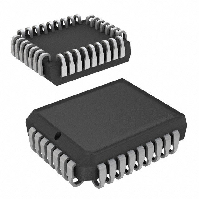
| 产品图片 |
|
| rohs | 符合RoHS |
| 产品系列 | 时钟和计时器IC,时钟驱动器及分配,IDT 8SLVP1204ANLGI |
| 产品型号 | 8SLVP1204ANLGI |
| 乘法/除法因子 | 2:4 |
| 产品种类 | 时钟驱动器及分配 |
| 商标 | IDT |
| 安装风格 | SMD/SMT |
| 封装 | Tube |
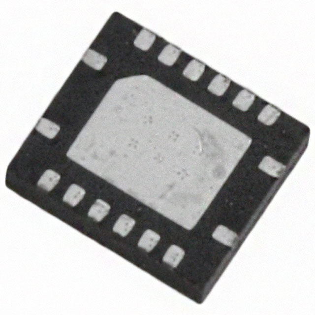
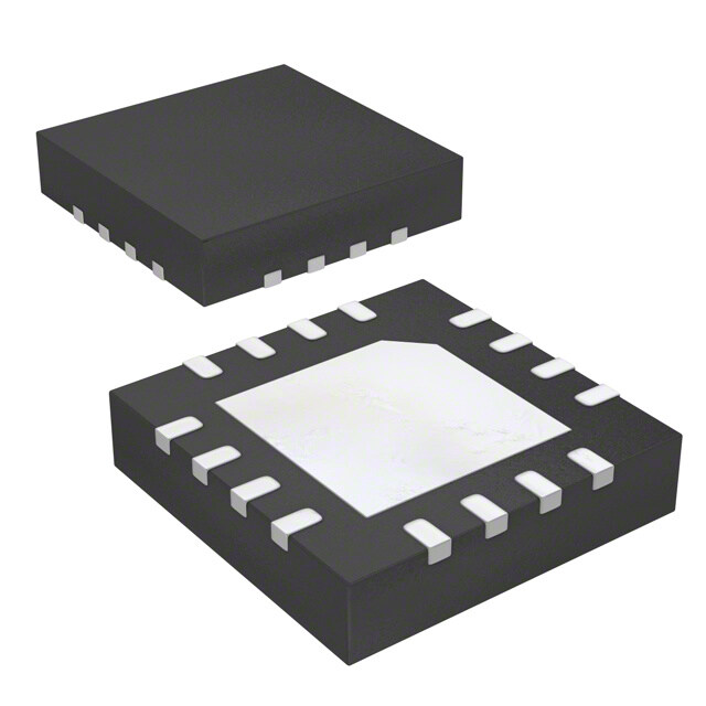
| 封装/箱体 | VFQFPN-16 |
| 工厂包装数量 | 100 |
| 最大工作温度 | + 85 C |
| 最大输出频率 | 2 GHz |
| 最小工作温度 | - 40 C |
| 电源电压-最大 | 3.63 V |
| 电源电压-最小 | 2.97 V |
| 电源电流 | 170 mA |
| 类型 | Fanout Buffers |
| 系列 | 8SLVP1204I |
| 输入类型 | LVCMOS |
| 输出类型 | LVPECL |
| 零件号别名 | 8SLVP1204I |


- 商务部:美国ITC正式对集成电路等产品启动337调查
- 曝三星4nm工艺存在良率问题 高通将骁龙8 Gen1或转产台积电
- 太阳诱电将投资9.5亿元在常州建新厂生产MLCC 预计2023年完工
- 英特尔发布欧洲新工厂建设计划 深化IDM 2.0 战略
- 台积电先进制程称霸业界 有大客户加持明年业绩稳了
- 达到5530亿美元!SIA预计今年全球半导体销售额将创下新高
- 英特尔拟将自动驾驶子公司Mobileye上市 估值或超500亿美元
- 三星加码芯片和SET,合并消费电子和移动部门,撤换高东真等 CEO
- 三星电子宣布重大人事变动 还合并消费电子和移动部门
- 海关总署:前11个月进口集成电路产品价值2.52万亿元 增长14.8%


PDF Datasheet 数据手册内容提取
Low Phase Noise, 2:4, 3.3V, 2.5V 8SLVP1204 LVPECL Output Fanout Buffer DATASHEET Description Features The 8SLVP1204 is a high-performance differential LVPECL fanout • Four low skew, low additive jitter LVPECL output pairs buffer. The device is designed for the fanout of high-frequency, very • Two selectable, differential clock input pairs low additive phase-noise clock and data signals. The 8SLVP1204 is • Differential PCLKx pairs can accept the following differential input characterized to operate from a 3.3V or 2.5V power supply. levels: LVDS, LVPECL, CML Guaranteed output-to-output and part-to-part skew characteristics make the 8SLVP1204 ideal for clock distribution applications that • Differential PCLKx pairs can also accept single-ended LVCMOS demand well-defined performance and repeatability. Two selectable levels. See Applications Information, “Wiring the Differential Input differential inputs and four low skew outputs are available. The to Accept Single-Ended Levels” (Figures 1A and 1B) integrated bias voltage reference enables easy interfacing of • Maximum input clock frequency: 2GHz single-ended signals to the device inputs. The device is optimized for low power consumption and low additive phase noise. • LVCMOS interface levels for the control input, (input select) • Output skew: 5ps (typical), at 3.63V • Propagation delay: 200ps (typical), at 3.63V • Low additive phase jitter, RMS; f = 156.25MHz, V = 1V, REF PP 12kHz - 20MHz: 40fs (maximum), at 3.63V • Maximum device current consumption (I ): 60mA (maximum), EE at 3.63V • Full 3.3V±5%, 3.3V±10% or 2.5V±5% supply • Lead-free (RoHS 6), 16-Lead VFQFPN packaging • -40°C to 85°C ambient operating temperature • Supports case temperature 105°C operations Block Diagram Pin Assignment 3 2 Q 3 Q 2 VCC n Q n Q 16 15 14 13 Pulldown Q0 VEE 1 12 nQ1 PCLK0 nPCLK0 Pullup/Pulldown nQ0 SEL 2 11 Q1 Q1 PCLK1 3 10 nQ0 0 fREF nQ1 nPCLK1 4 9 Q0 5 6 7 8 1 Q2 VCC nQ2 CC K0 K0 EF Pulldown V CL CL VR PCLK1 P P Pullup/Pulldown Q3 n nPCLK1 nQ3 8SLVP1204 16-Lead, 3mm x 3mm VFQFPN Package Pulldown SEL Voltage V REF Reference IDT8SLVP1204 NOVEMBER 29, 2018 1 ©2018 Integrated Device Technology, Inc.
8SLVP1204 DATASHEET Pin Descriptions and Characteristics Table 1. Pin Descriptions Number Name Type Description 1 VEE Power Negative supply pin. Reference select control pin. See Table 3 for function. LVCMOS/LVTTL interface 2 SEL Input Pulldown levels. 3 PCLK1 Input Pulldown Non-inverting differential LVPECL clock/data input. Pullup/ 4 nPCLK1 Input Inverting differential LVPECL clock/data input. V /2 default when left floating. Pulldown CC 5 VCC Power Power supply pins. 6 PCLK0 Input Pulldown Non-inverting differential LVPECL clock/data input. Pullup/ 7 nPCLK0 Input Inverting differential LVPECL clock/data input. V /2 default when left floating. Pulldown CC 8 VREF Output Bias voltage reference for the PCLK inputs. 9, 10 Q0, nQ0 Output Differential output pair 0. LVPECL interface levels. 11, 12 Q1, nQ1 Output Differential output pair 1. LVPECL interface levels. 13, 14 Q2, nQ2 Output Differential output pair 2. LVPECL interface levels. 15, 16 Q3, nQ3 Output Differential output pair 3. LVPECL interface levels. NOTE: Pulldown and Pullup refers to an internal input resistors. See Table 2, Pin Characteristics, for typical values. Table 2. Pin Characteristics Symbol Parameter Test Conditions Minimum Typical Maximum Units C Input Capacitance 2 pF IN R Input Pulldown Resistor 51 k PULLDOWN R Input Pullup Resistor 51 k PULLUP Function Table Table 3. SEL Input Selection Function Table Input SEL Operation 0 (default) PCLK0, nPCLK0 is the selected differential clock input. 1 PCLK1, nPCLK1 is the selected differential clock input. NOTE: SEL is an asynchronous control. IDT8SLVP1204 NOVEMBER 29, 2018 2 ©2018 Integrated Deice Technology, Inc.
8SLVP1204 DATASHEET Absolute Maximum Ratings Exposure to absolute maximum rating conditions for extended periods may affect product reliability. Stresses beyond those listed under Absolute Maximum Ratings may cause permanent damage to the device. These ratings are stress specifications only. Functional operation of the product at these conditions or any conditions beyond those listed in the DC Characteristics or AC Characteristics is not implied. Item Rating Supply Voltage, V 4.6V CC Inputs, V -0.5V to V + 0.5V I CC Outputs, I (LVPECL) O Continuous Current 50mA Surge Current 100mA Input Sink/Source, I ±2mA REF Maximum Junction Temperature, T 150°C J,MAX Storage Temperature, T -65°C to 150°C STG ESD - Human Body Model, NOTE 1 2000V ESD - Charged Device Model, NOTE 1 1500V NOTE 1: According to JEDEC/JESD 22-A114/22-C101. Recommended Operating Conditions Symbol Parameter Minimum Typical Maximum Units T Ambient air temperature -40 85 C A T Junction temperature 125 C J NOTE 1: It is the user’s responsibility to ensure that device junction temperature remains below the maximum allowed. NOTE 2: All conditions in the table must be met to guarantee device functionality. NOTE 3: The device is verified to the maximum operating junction temperature through simulation. DC Electrical Characteristics Table 4A. Power Supply DC Characteristics, V = 3.3V ±10%, V = 0V, T = -40°C to 85°C CC EE A Symbol Parameter Test Conditions Minimum Typical Maximum Units V Power Supply Voltage 2.97 3.3V 3.63 V CC I Power Supply Current 53 60 mA EE I Power Supply Current Q0 to Q3 terminated 50 to V – 2V 170 204 mA CC CC Table 4B. Power Supply DC Characteristics, V = 3.3V ±5%, V = 0V, T = -40°C to 85°C CC EE A Symbol Parameter Test Conditions Minimum Typical Maximum Units V Power Supply Voltage 3.135 3.3V 3.465 V CC I Power Supply Current 53 60 mA EE I Power Supply Current Q0 to Q3 terminated 50 to V – 2V 170 204 mA CC CC IDT8SLVP1204 NOVEMBER 29, 2018 3 ©2018 Integrated Device Technology, Inc.
8SLVP1204 DATASHEET Table 4C. Power Supply DC Characteristics, V = 2.5V ±5%, V = 0V, T = -40°C to 85°C CC EE A Symbol Parameter Test Conditions Minimum Typical Maximum Units V Power Supply Voltage 2.375 2.5V 2.625 V CC I Power Supply Current 49 55 mA EE I Power Supply Current Q0 to Q3 terminated 50 to V – 2V 170 199 mA CC CC Table 4D. LVCMOS/LVTTL DC Characteristics, V = 3.3V ±10%, V = 0V, T = -40°C to 85°C CC EE A Symbol Parameter Test Conditions Minimum Typical Maximum Units V = 3.63V 2.2 V + 0.3 V CC CC V Input High Voltage IH V = 2.625V 1.7 V + 0.3 V CC CC V = 3.63V -0.3 0.8 V CC V Input Low Voltage IL V = 2.625V -0.3 0.7 V CC I Input High Current SEL V = V = 3.465V or 2.625V 150 µA IH CC IN I Input Low Current SEL V = 3.465V or 2.625V, V = 0V -10 µA IL CC IN Table 4E. LVCMOS/LVTTL DC Characteristics, V = 3.3V ±5% or 2.5V ±5%, V = 0V, T = -40°C to 85°C CC EE A Symbol Parameter Test Conditions Minimum Typical Maximum Units V = 3.465V 2.2 V + 0.3 V CC CC V Input High Voltage IH V = 2.625V 1.7 V + 0.3 V CC CC V = 3.465V -0.3 0.8 V CC V Input Low Voltage IL V = 2.625V -0.3 0.7 V CC I Input High Current SEL V = V = 3.465V or 2.625V 150 µA IH CC IN I Input Low Current SEL V = 3.465V or 2.625V, V = 0V -10 µA IL CC IN IDT8SLVP1204 NOVEMBER 29, 2018 4 ©2018 Integrated Device Technology, Inc.
8SLVP1204 DATASHEET Table 4F. LVPECL DC Characteristics, V = 3.3V ±10%, V = 0V, T = -40°C to 85°C CC EE A Symbol Parameter Test Conditions Minimum Typical Maximum Units PCLK0, nPCLK0 I Input High Current V = V = 3.63V 150 µA IH PCLK1, nPCLK1 CC IN PCLK0, PCLK1 V = 3.63V, V = 0V -10 µA CC IN I Input Low Current IL nPCLK0, nPCLK1 V = 3.63V, V = 0V -150 µA CC IN V Reference Voltage for Input Bias I = ±1mA V – 1.6 V – 1.3 V – 1.1 V REF REF CC CC CC V Output High Voltage1 V – 1.1 V – 0.9 V – 0.7 V OH CC CC CC V Output Low Voltage1 V – 2.0 V – 1.65 V – 1.5 V OL CC CC CC NOTE 1. Outputs terminated with 50 to V – 2V. CC Table 4G. LVPECL DC Characteristics, V = 3.3V ±5%, V = 0V, T = -40°C to 85°C CC EE A Symbol Parameter Test Conditions Minimum Typical Maximum Units PCLK0, nPCLK0 I Input High Current V = V = 3.465V 150 µA IH PCLK1, nPCLK1 CC IN PCLK0, PCLK1 V = 3.465V, V = 0V -10 µA CC IN I Input Low Current IL nPCLK0, nPCLK1 V = 3.465V, V = 0V -150 µA CC IN V Reference Voltage for Input Bias I = ±1mA V – 1.6 V – 1.3 V – 1.1 V REF REF CC CC CC V Output High Voltage1 V – 1.1 V – 0.9 V – 0.7 V OH CC CC CC V Output Low Voltage1 V – 2.0 V – 1.65 V – 1.5 V OL CC CC CC NOTE 1. Outputs terminated with 50 to V – 2V. CC Table 4H. LVPECL DC Characteristics, V = 2.5V ±5%, V = 0V, T = -40°C to 85°C CC EE A Symbol Parameter Test Conditions Minimum Typical Maximum Units PCLK0, nPCLK0 I Input High Current V = V = 2.625V 150 µA IH PCLK1, nPCLK1 CC IN PCLK0, PCLK1 V = 2.625V, V = 0V -10 µA CC IN I Input Low Current IL nPCLK0, nPCLK1 V = 2.625V, V = 0V -150 µA CC IN V Reference Voltage for Input Bias I = ±1mA V – 1.6 V – 1.3 V – 1.1 V REF REF CC CC CC V Output High Voltage1 V – 1.1 V – 0.9 V – 0.7 V OH CC CC CC V Output Low Voltage1 V – 2.0 V – 1.6 V – 1.5 V OL CC CC CC NOTE 1. Outputs terminated with 50 to V – 2V. CC IDT8SLVP1204 NOVEMBER 29, 2018 5 ©2018 Integrated Device Technology, Inc.
8SLVP1204 DATASHEET AC Electrical Characteristics Table 5A. AC Electrical Characteristics, V = 3.3V ± 5% or 2.5V ±5%, V = 0V, T = -40°C to 85°C1 CC EE A Symbol Parameter Test Conditions Minimum Typical Maximum Units Input PCLK[0:1], f 2 GHz REF Frequency nPCLK[0:1] Input PCLK[0:1], V/t 1.5 V/ns Edge Rate nPCLK[0:1] PCKx, nPCLKx to any Qx, nQx t Propagation Delay2 120 200 320 ps PD for V = 0.1V or 0.3V PP tsk(o) Output Skew3 4 5 25 ps tsk(i) Input Skew4 5 50 ps tsk(p) Pulse Skew f = 100MHz 5 20 ps REF tsk(pp) Part-to-Part Skew4 5 100 200 ps f = 122.88MHz Sine Wave, V = 1V, REF PP 170 fs Integration Range: 1kHz – 40MHz f = 122.88MHz Sine Wave, V = 1V, REF PP 114 fs Integration Range: 10kHz – 20MHz f = 122.88MHz Sine Wave, V = 1V, REF PP 114 fs Integration Range: 12kHz – 20MHz f = 156.25MHz Square Wave, REF V = 1V, Integration Range: 42 51 fs PP 1kHz – 40MHz f = 156.25MHz Square Wave, REF Buffer Additive Phase V = 1V, Integration Range: 32 40 fs PP Jitter, RMS; refer to 10kHz – 20MHz t JIT Additive Phase Jitter f = 156.25MHz Square Wave, REF Section V = 1V, Integration Range: 32 40 fs PP 12kHz – 20MHz f = 156.25MHz Square Wave, REF V = 0.5V, Integration Range: 51 71 fs PP 1kHz – 40MHz f = 156.25MHz Square Wave, REF V = 0.5V, Integration Range: 38 52 fs PP 10kHz – 20MHz f = 156.25MHz Square Wave, REF V = 0.5V, Integration Range: 38 52 fs PP 12kHz – 20MHz t / t Output Rise/ Fall Time 20% to 80% 35 90 180 ps R F MUX Mux Isolation6 f = 100MHz 77 dB ISOLATION REF Peak-to-Peak Input fREF < 1.5 GHz 0.1 1.5 V V PP Voltage7 f > 1.5 GHz 0.2 1.5 V REF Common Mode Input 1.0 VCC – 0.6 V V CMR Voltage7 89 V = > 247mV 0.8 V – 0.6 V PP CC Output Voltage Swing, VCC = 3.3V, fREF 2GHz 0.45 0.75 1.0 V V (pp) O Peak-to-Peak V = 2.5V, f 2GHz 0.4 0.65 1.0 V CC REF Differential Output V = 3.3V, f 2GHz 0.9 1.5 2.0 V CC REF V Voltage Swing, DIFF_OUT V = 2.5V, f 2GHz 0.8 1.3 2.0 V Peak-to-Peak CC REF IDT8SLVP1204 NOVEMBER 29, 2018 6 ©2018 Integrated Device Technology, Inc.
8SLVP1204 DATASHEET NOTE 1. Electrical parameters are guaranteed over the specified ambient operating temperature range, which is established when the device is mounted in a test socket with maintained transverse airflow greater than 500 lfpm. The device will meet specifications after thermal equilibrium has been reached under these conditions. NOTE 2. Measured from the differential input crossing point to the differential output crosspoint. NOTE 3. Defined as skew between outputs at the same supply voltage and with equal load conditions. Measured at the differential cross point. NOTE 4. This parameter is defined in accordance with JEDEC Standard 65. NOTE 5. Defined as skew between outputs on different devices operating at the same supply voltage, same frequency, same temperature and with equal load conditions. Using the same type of inputs on each device, the outputs are measured at the differential cross point. NOTE 6. Qx, nQx outputs measured differentially. See MUX Isolation diagram in the Parameter Measurement Information section. NOTE 7. For single-ended LVCMOS input applications, refer to the Applications section Wiring the Differential Input Levels to Accept Sin- gle-ended Levels (Figures 1 and 2). NOTE 8. V should not be less than -0.3V. V should not be higher than V . IL IH CC NOTE 9. Common mode input voltage is defined as the crosspoint. Table 5B. AC Electrical Characteristics, V = 3.3V ±10%, V = 0V, T = -40°C to 85°C1 CC EE A Symbol Parameter Test Conditions Minimum Typical Maximum Units Input PCLK[0:1], f 2 GHz REF Frequency nPCLK[0:1] Input2 PCLK[0:1], V/t 1.5 V/ns Edge Rate nPCLK[0:1] PCKx, nPCLKx to any Qx, nQx t Propagation Delay3 120 230 325 ps PD for V = 0.1V or 0.3V PP tsk(o) Output Skew4 5 6 30 ps tsk(i) Input Skew4 6 55 ps tsk(p) Pulse Skew f = 100MHz 7 25 ps REF tsk(pp) Part-to-Part Skew4 6 200 ps t / t Output Rise/ Fall Time 20% to 80% 35 200 ps R F MUX Mux Isolation7 f = 100MHz 77 dB ISOLATION REF Peak-to-Peak Input fREF < 1.5 GHz 0.1 1.5 V V PP Voltage8 f > 1.5 GHz 0.2 1.5 V REF Common Mode Input 1.0 VCC – 0.6 V V CMR Voltage7 910 V = > 247mV 0.8 V – 0.6 V PP CC Output Voltage Swing, VCC = 3.3V, fREF 2GHz 0.45 0.75 1.0 V V (pp) O Peak-to-Peak V = 2.5V, f 2GHz 0.4 0.65 1.0 V CC REF Differential Output V = 3.3V, f 2GHz 0.9 1.5 2.0 V CC REF V Voltage Swing, DIFF_OUT V = 2.5V, f 2GHz 0.8 1.3 2.0 V Peak-to-Peak CC REF NOTE 1. Electrical parameters are guaranteed over the specified ambient operating temperature range, which is established when the device is mounted in a test socket with maintained transverse airflow greater than 500 lfpm. The device will meet specifications after thermal equilibrium has been reached under these conditions. NOTE 2. Input Edge Rate is the slope of Δv/Δt at the crosspoint of the differential pair signals. Δt is measured with ΔV = 300mV on one of the single-ended input pair signals. NOTE 3. Measured from the differential input crossing point to the differential output crosspoint. NOTE 4. Defined as skew between outputs at the same supply voltage and with equal load conditions. Measured at the differential cross point. NOTE 5. This parameter is defined in accordance with JEDEC Standard 65 IDT8SLVP1204 NOVEMBER 29, 2018 7 ©2018 Integrated Device Technology, Inc.
8SLVP1204 DATASHEET NOTE 6. Defined as skew between outputs on different devices operating at the same supply voltage, same frequency, same temperature and with equal load conditions. Using the same type of inputs on each device, the outputs are measured at the differential cros- spoint. NOTE 7. Qx, nQx outputs measured differentially. See MUX Isolation diagram in the Parameter Measurement Information section. NOTE 8. For single-ended LVCMOS input applications, refer to the Applications section Wiring the Differential Input Levels to Accept Sin- gle-ended Levels (Figures 1 and 2). NOTE 9. V should not be less than -0.3V. V should not be higher than V . IL IH CC NOTE 10. Common mode input voltage is defined as the crosspoint. IDT8SLVP1204 NOVEMBER 29, 2018 8 ©2018 Integrated Device Technology, Inc.
8SLVP1204 DATASHEET Additive Phase Jitter The spectral purity in a band at a specific offset from the fundamental of the power in the 1Hz band to the power in the fundamental. When compared to the power of the fundamental is called the dBc Phase the required offset is specified, the phase noise is called a dBc value, Noise. This value is normally expressed using a Phase noise plot which simply means dBm at a specified offset from the fundamental. and is most often the specified plot in many applications. Phase noise By investigating jitter in the frequency domain, we get a better is defined as the ratio of the noise power present in a 1Hz band at a understanding of its effects on the desired application over the entire specified offset from the fundamental frequency to the power value of time record of the signal. It is mathematically possible to calculate an the fundamental. This ratio is expressed in decibels (dBm) or a ratio expected bit error rate given a phase noise plot. z H c/ B d e s oi N e s a h P B S S Offset from Carrier Frequency (Hz) As with most timing specifications, phase noise measurements has Measured using a Wenzel 156.25MHz Oscillator as the input source. issues relating to the limitations of the equipment. Often the noise floor of the equipment is higher than the noise floor of the device. This is illustrated above. The device meets the noise floor of what is shown, but can actually be lower. The phase noise is dependent on the input source and measurement equipment. IDT8SLVP1204 NOVEMBER 29, 2018 9 ©2018 Integrated Device Technology, Inc.
8SLVP1204 DATASHEET Parameter Measurement Information 2V 2V SCOPE SCOPE VCC Qx VCC Qx nQx nQx V V EE EE -1.3V±0.33V -1.3V±0.165V 3.3V ±10% LVPECL Output Load Test Circuit 3.3V ±5% LVPECL Output Load Test Circuit 2V VCC SCOPE VCC Qx nPCLK[0:1] PCLK[0:1] nQx VEE VEE -0.5V±0.125V 2.5V LVPECL Output Load Test Circuit Differential Input Level nPCLK[0:1] Part 1 nQx PCLK[0:1] Qx nQy Part 2 nQy Qy Qy tPLH tPHL tsk(pp) tsk(p)=|t -t | PHL PLH Part-to-Part Skew Pulse Skew IDT8SLVP1204 NOVEMBER 29, 2018 10 ©2018 Integrated Device Technology, Inc.
8SLVP1204 DATASHEET Parameter Measurement Information, continued nPCLK0 Spectrum of Output Signal Q PCLK0 A0 MUX selects active input clock signal nPCLK1 B) d PCLK1 de ( plitu MUX_ISOLATION = A0 – A1 nQ[0:3] m A A1 MUX selects other input Q[0:3] t PD2 t PD1 tsk(i) ƒ Frequency (fundamental) tsk(i) = |t - t | PD1 PD2 Input Skew MUX Isolation nQx nPCLK[0:1] Qx PCLK[0:1] nQy nQ[0:3] Qy Q[0:3] t PD Output Skew Propagation Delay nQ[0:3] 80% 80% V O(PP) 20% 20% Q[0:3] t t R F Output Rise/Fall Time IDT8SLVP1204 NOVEMBER 29, 2018 11 ©2018 Integrated Device Technology, Inc.
8SLVP1204 DATASHEET Applications Information Wiring the Differential Input to Accept Single-Ended Levels The 8SLVP1204 inputs can be interfaced to LVPECL, LVDS, CML or LVCMOS drivers. Figure 1A illustrates how to DC couple a single LVCMOS input to the 8SLVP1204. The value of the series resistance RS is calculated as the difference between the transmission line impedance and the driver output impedance. This resistor should be placed close to the LVCMOS driver. To avoid cross-coupling of single-ended LVCMOS signals, apply the LVCMOS signals to no more than one PCLK input. A practical method to implement Vth is shown in Figure 1B below. The reference voltage Vth = V1 = V /2, is generated by the bias CC resistors R1 and R2. The bypass capacitor (C1) is used to help filter noise on the DC bias. This bias circuit should be located as close to the input pin as possible. The ratio of R1 and R2 might need to be adjusted to position the V1 in the center of the input voltage swing. For example, if the input clock swing is 2.5V and V = 3.3V, R1 and R2 value should be adjusted CC to set V1 at 1.25V. The values below apply when both the Figure 1A. DC-Coupling a Single LVCMOS Input to the single-ended swing and VCC are at the same voltage. 8SLVP1204 When using single-ended signaling, the noise rejection benefits of This configuration requires that the sum of the output impedance of differential signaling are reduced. Even though the differential input the driver (Ro) and the series resistance (Rs) equals the transmission can handle full rail LVCMOS signaling, it is recommended that the line impedance. R3 and R4 in parallel should equal the transmission amplitude be reduced, particularly if both input references are line impedance; for most 50 applications, R3 and R4 will be 100. LVCMOS to minimize cross talk. The datasheet specifies a lower The values of the resistors can be increased to reduce the loading for differential amplitude, however this only applies to differential signals. slower and weaker LVCMOS driver. For single-ended applications, the swing can be larger, however V IL Though some of the recommended components of Figure 1B might cannot be less than -0.3V and V cannot be more than V + 0.3V. IH CC not be used, the pads should be placed in the layout so that they can Figure 1B shows a way to attenuate the PCLK input level by a factor be utilized for debugging purposes. The datasheet specifications are of two as well as matching the transmission line between the characterized and guaranteed by using a differential signal. LVCMOS driver and the 8SLVP1204 at both the source and the load. VCC VCC VCC VCC R3 100 R1 1K Ro RS Zo = 50 Ohm + Receiver Driver V1 R4 - 100 Ro + Rs = Zo R2 C1 1K 0.1uF Figure 1B. Alternative DC Coupling a Single LVCMOS Input to the 8SLVP1204 IDT8SLVP1204 NOVEMBER 29, 2018 12 ©2018 Integrated Device Technology, Inc.
8SLVP1204 DATASHEET 3.3V LVPECL Clock Input Interface The PCLK /nPCLK accepts LVPECL, LVDS, CML and other input interfaces suggested here are examples only. If the driver is differential signals. Both signals must meet the V and V input from another vendor, use their termination recommendation. Please PP CMR requirements. Figures 2A to 2E show interface examples for the consult with the vendor of the driver component to confirm the driver PCLK/ nPCLK input driven by the most common driver types. The termination requirements. 3.3V 3.3V 3.3V 3.3V Zo = 50Ω 3.3V PCLK PCLK R1 100Ω nPCLK Zo = 50Ω nPCLK CML LVPECL CML Built-In Pullup LVPECL Input Input Figure 2A. PCLK/nPCLK Input Driven by a CML Driver Figure 2B. PCLK/nPCLK Input Driven by a Built-In Pullup CML Driver 3.3V 3.3V 3.3V R3 R4 125Ω 125Ω Zo = 50Ω PCLK Zo = 50Ω nPCLK LVPECL LVPECL Input R1 R2 84Ω 84Ω Figure 2C. PCLK/nPCLK Input Driven by a Figure 2D. PCLK/nPCLK Input Driven by a 3.3V LVPECL Driver 3.3V LVPECL Driver with AC Couple 3.3V 3.3V Zo = 50Ω PCLK R1 100Ω Zo = 50Ω nPCLK LVPECL LVDS Input Figure 2E. PCLK/nPCLK Input Driven by a 3.3V LVDS Driver IDT8SLVP1204 NOVEMBER 29, 2018 13 ©2018 Integrated Device Technology, Inc.
8SLVP1204 DATASHEET 2.5V LVPECL Clock Input Interface The PCLK /nPCLK accepts LVPECL, LVDS, CML and other input interfaces suggested here are examples only. If the driver is differential signals. Both signals must meet the V and V input from another vendor, use their termination recommendation. Please PP CMR requirements. Figures 3A to 3E show interface examples for the consult with the vendor of the driver component to confirm the driver PCLK/ nPCLK input driven by the most common driver types. The termination requirements. 2.5V 2.5V 2.5V 2.5V 2.5V PCLK PCLK nPCLK CML nPCLK LVPECL CML Built-In Pullup LVPECL Input Input Figure 3A. PCLK/nPCLK Input Driven by a CML Driver Figure 3B. PCLK/nPCLK Input Driven by a Built-In Pullup CML Driver 2.5V 2.5V 2.5V PCLK nPCLK LVPECL LVPECL Input Figure 3C. PCLK/nPCLK Input Driven by a Figure 3D. PCLK/nPCLK Input Driven by a 2.5V LVPECL Driver 2.5V LVPECL Driver with AC Couple PCLK nPCLK Figure 3E. PCLK/nPCLK Input Driven by a 2.5V LVDS Driver IDT8SLVP1204 NOVEMBER 29, 2018 14 ©2018 Integrated Device Technology, Inc.
8SLVP1204 DATASHEET Recommendations for Unused Input and Output Pins Inputs: Outputs: PCLK/nPCLK Inputs LVPECL Outputs For applications not requiring the use of a differential input, both the All unused LVPECL output pairs can be left floating. We recommend PCLK and nPCLK pins can be left floating. Though not required, but that there is no trace attached. Both sides of the differential output for additional protection, a 1k resistor can be tied from PCLK to pair should either be left floating or terminated. ground. VFQFPN EPAD Thermal Release Path In order to maximize both the removal of heat from the package and and dependent upon the package power dissipation as well as the electrical performance, a land pattern must be incorporated on electrical conductivity requirements. Thus, thermal and electrical the Printed Circuit Board (PCB) within the footprint of the package analysis and/or testing are recommended to determine the minimum corresponding to the exposed metal pad or exposed heat slug on the number needed. Maximum thermal and electrical performance is package, as shown in Figure 4. The solderable area on the PCB, as achieved when an array of vias is incorporated in the land pattern. It defined by the solder mask, should be at least the same size/shape is recommended to use as many vias connected to ground as as the exposed pad/slug area on the package to maximize the possible. It is also recommended that the via diameter should be 12 thermal/electrical performance. Sufficient clearance should be to 13mils (0.30 to 0.33mm) with 1oz copper via barrel plating. This is designed on the PCB between the outer edges of the land pattern desirable to avoid any solder wicking inside the via during the and the inner edges of pad pattern for the leads to avoid any shorts. soldering process which may result in voids in solder between the exposed pad/slug and the thermal land. Precautions should be taken While the land pattern on the PCB provides a means of heat transfer to eliminate any solder voids between the exposed heat slug and the and electrical grounding from the package to the board through a land pattern. Note: These recommendations are to be used as a solder joint, thermal vias are necessary to effectively conduct from guideline only. For further information, please refer to the Application the surface of the PCB to the ground plane(s). The land pattern must Note on the Surface Mount Assembly of Amkor’s Thermally/ be connected to ground through these vias. The vias act as “heat Electrically Enhance Leadframe Base Package, Amkor Technology. pipes”. The number of vias (i.e. “heat pipes”) are application specific SOLDER SOLDER PIN EXPOSED HEAT SLUG PIN PIN PAD GROUND PLANE LAND PATTERN PIN PAD THERMAL VIA (GROUND PAD) Figure 4. P.C. Assembly for Exposed Pad Thermal Release Path – Side View (drawing not to scale) IDT8SLVP1204 NOVEMBER 29, 2018 15 ©2018 Integrated Device Technology, Inc.
8SLVP1204 DATASHEET Termination for 3.3V LVPECL Outputs The clock layout topology shown below is a typical termination for transmission lines. Matched impedance techniques should be used LVPECL outputs. The two different layouts mentioned are to maximize operating frequency and minimize signal distortion. recommended only as guidelines. Figures 5A and 5B show two different layouts which are recommended only as guidelines. Other suitable clock layouts may The differential outputs are a low impedance follower output that exist and it would be recommended that the board designers generate ECL/LVPECL compatible outputs. Therefore, terminating simulate to guarantee compatibility across all printed circuit and clock resistors (DC current path to ground) or current sources must be component process variations. used for functionality. These outputs are designed to drive 50 3.3V R3 R4 125Ω 125Ω 3.3V 3.3V Z = 50Ω o + _ Input Z = 50Ω o R1 R2 84Ω 84Ω Figure 5A. 3.3V LVPECL Output Termination Figure 5B. 3.3V LVPECL Output Termination IDT8SLVP1204 NOVEMBER 29, 2018 16 ©2018 Integrated Device Technology, Inc.
8SLVP1204 DATASHEET Termination for 2.5V LVPECL Outputs Figure 6A and Figure 6B show examples of termination for 2.5V level. The R3 in Figure 6B can be eliminated and the termination is LVPECL driver. These terminations are equivalent to terminating 50 shown in Figure 6C. to V – 2V. For V = 2.5V, the V – 2V is very close to ground CC CC CC 2.5V 2.5V VCC = 2.5V 2.5V VCC = 2.5V R1 R3 50Ω 250Ω 250Ω + 50Ω + 50Ω – 50Ω 2.5V LVPECL Driver – R1 R2 2.5V LVPECL Driver 50Ω 50Ω R2 R4 62.5Ω 62.5Ω R3 18Ω Figure 6A. 2.5V LVPECL Driver Termination Example Figure 6B. 2.5V LVPECL Driver Termination Example 2.5V VCC = 2.5V 50Ω + 50Ω – 2.5V LVPECL Driver R1 R2 50Ω 50Ω Figure 6C. 2.5V LVPECL Driver Termination Example IDT8SLVP1204 NOVEMBER 29, 2018 17 ©2018 Integrated Device Technology, Inc.
8SLVP1204 DATASHEET 3.3V ±10% Power Considerations This section provides information on power dissipation and junction temperature for the 8SLVP1204. Equations and example calculations are also provided. 1. Power Dissipation. The total power dissipation for the 8SLVP1204 is the sum of the core power plus the power dissipated due to loading. The following is the power dissipation for V = 3.63V. CC NOTE: Please refer to Section 3 for details on calculating power dissipated due to loading. The maximum current at 85° is as follows: I = 65mA EE_MAX • Power (core) = V * I = 3.63V * 60mA = 217.80mW MAX CC_MAX EE_MAX • Power (outputs) = 33.2mW/Loaded Output pair MAX If all outputs are loaded, the total power is 4 * 33.2mW = 132.8mW Total Power_ (3.63V, with all outputs switching) = 217.80mW + 132.8mW = 350.60mW MAX 2. Junction Temperature. Junction temperature, Tj, is the temperature at the junction of the bond wire and bond pad directly affects the reliability of the device. The maximum recommended junction temperature is 125°C. Limiting the internal transistor junction temperature, Tj, to 125°C ensures that the bond wire and bond pad temperature remains below 125°C. The equation for Tj is as follows: Tj = * Pd_total + T JA A Tj = Junction Temperature = Junction-to-Ambient Thermal Resistance JA Pd_total = Total Device Power Dissipation (example calculation is in section 1 above) T = Ambient Temperature A In order to calculate junction temperature, the appropriate junction-to-ambient thermal resistance must be used. Assuming no air flow and JA a multi-layer board, the appropriate value is 74.7°C/W per Table 6 below. Therefore, Tj for an ambient temperature of 85°C with all outputs switching is: 85°C + 0.351W * 74.7°C/W = 111.2°C. This is below the limit of 125°C. This calculation is only an example. Tj will obviously vary depending on the number of loaded outputs, supply voltage, air flow and the type of board (multi-layer). Table 6. Thermal Resistance for 16-Lead VFQFPN, Forced Convection JA by Velocity JA Meters per Second 0 1 2.5 Multi-Layer PCB, JEDEC Standard Test Boards 74.7°C/W 65.3°C/W 58.5°C/W IDT8SLVP1204 NOVEMBER 29, 2018 18 ©2018 Integrated Device Technology, Inc.
8SLVP1204 DATASHEET 3.Calculations and Equations. The purpose of this section is to calculate the power dissipation for the LVPECL output pair. LVPECL output driver circuit and termination are shown in Figure 7. V CC Q1 V OUT RL V - 2V CC Figure 7. LVPECL Driver Circuit and Termination To calculate power dissipation due to loading, use the following equations which assume a 50 load, and a termination voltage of V – 2V. CC These are typical calculations. • For logic high, V = V = V – 0.7V OUT OH_MAX CC_MAX (V – V ) = 0.7V CC_MAX OH_MAX • For logic low, V = V = V – 1.5V OUT OL_MAX CC_MAX (V – V ) = 1.5V CC_MAX OL_MAX Pd_H is power dissipation when the output drives high. Pd_L is the power dissipation when the output drives low. Pd_H = [(V – (V – 2V))/R ] * (V – V ) = [(2V – (V – V ))/R ] * (V – V ) = OH_MAX CC_MAX L CC_MAX OH_MAX CC_MAX OH_MAX L CC_MAX OH_MAX [(2V – 0.7V)/50] * 0.7V = 18.2mW Pd_L = [(V – (V – 2V))/R ] * (V – V ) = [(2V – (V – V ))/R ] * (V – V ) = OL_MAX CC_MAX L CC_MAX OL_MAX CC_MAX OL_MAX L CC_MAX OL_MAX [(2V – 1.5V)/50] * 1.5V = 15mW Total Power Dissipation per output pair = Pd_H + Pd_L = 33.2mW IDT8SLVP1204 NOVEMBER 29, 2018 19 ©2018 Integrated Device Technology, Inc.
8SLVP1204 DATASHEET Case Temperature Considerations This device supports applications in a natural convection environment which does not have any thermal conductivity through ambient air. The printed circuit board (PCB) is typically in a sealed enclosure without any natural or forced air flow and is kept at or below a specific temperature. The device package design incorporates an exposed pad (ePad) with enhanced thermal parameters which is soldered to the PCB where most of the heat escapes from the bottom exposed pad. For this type of application, it is recommended to use the junction-to-board thermal characterization parameter (Psi-JB) to calculate the junction temperature (T ) and ensure it does not exceed the maximum allowed JB J junction temperature in the Absolute Maximum Rating table. The junction-to-board thermal characterization parameter, , is calculated using the following equation: JB T = T + x P , Where J CB JB d T = Junction temperature at steady state condition in (oC). J T = Case temperature (Bottom) at steady state condition in (oC). CB =Thermal characterization parameter to report the difference between junction temperature and the temperature of the board JB measured at the top surface of the board. P = power dissipation (W) in desired operating configuration. d T J T CB The ePad provides a low thermal resistance path for heat transfer to the PCB and represents the key pathway to transfer heat away from the IC to the PCB. It’s critical that the connection of the exposed pad to the PCB is properly constructed to maintain the desired IC case temperature (T ). A good connection ensures that temperature at the exposed pad (T ) and the board temperature (T ) are relatively the same. An CB CB B improper connection can lead to increased junction temperature, increased power consumption and decreased electrical performance. In addition, there could be long-term reliability issues and increased failure rate. Example Calculation for Junction Temperature (T ): T = T + x P J J CB JB d Package type: 16-Lead VFQFPN Body size: 3mm x 3mm x0.9mm ePad size: 1.7mm x 1.7mm Thermal Via: 2 x 2 matrix 5.1 C/W JB T 105oC CB Pd 0.351 W For the variables above, the junction temperature is equal to 107oC. Since this is below the maximum junction temperature of 125oC, there are no long term reliability concerns. In addition, since the junction temperature at which the device was characterized using forced convection is 111.2oC, this device can function without the degradation of the specified AC or DC parameters. IDT8SLVP1204 NOVEMBER 29, 2018 20 ©2018 Integrated Device Technology, Inc.
8SLVP1204 DATASHEET Reliability Information Table 7. vs. Air Flow Table for a 16-Lead VFQFPN JA at 0 Air Flow JA Meters per Second 0 1 2.5 Multi-Layer PCB, JEDEC Standard Test Boards 74.7°C/W 65.3°C/W 58.5°C/W Transistor Count The transistor count for the 8SLVP1204 is: 258 Package Outline Drawings The package outline drawings are appended at the end of this document and are accessible from the link below. The package information is the most current data available. www.idt.com/document/psc/16-vfqfpn-package-outline-drawing-30-x-30-x-09-mm-05-mm-170-x-170-mm-epad-nlnlg16p2 Ordering Information Table 8. Ordering Information Part/Order Number Marking Package Shipping Packaging Temperature 8SLVP1204ANLGI 204AI 16-VFQFPN, Lead-Free Tube -40°C to 85°C 8SLVP1204ANLGI8 204AI 16-VFQFPN, Lead-Free Tape & Reel, Pin 1 Orientation: EIA-481-C -40°C to 85°C 8SLVP1204ANLGI/W 204AI 16-VFQFPN, Lead-Free Tape & Reel, Pin 1 Orientation: EIA-481-D -40°C to 85°C Table 9. Pin 1 Orientation in Tape and Reel Packaging Part Number Suffix Pin 1 Orientation Illustration 8 Quadrant 1 (EIA-481-C) /W Quadrant 2 (EIA-481-D) IDT8SLVP1204 NOVEMBER 29, 2018 21 ©2018 Integrated Device Technology, Inc.
8SLVP1204 DATASHEET Revision History Revision Date Description of Change Updated the description of Absolute Maximum Ratings November 29, 2018 Added Recommended Operating Conditions September 13, 2018 Added Note 2 to Table 5B. Updated the package outline drawings; however, no technical changes March 13, 2018 Completed other minor changes Features Section - Added Case Temperature bullet. June 8, 2015 Added Case Temperature Considerations. AC Characteristic Tables - added V spec. December 19, 2014 CMR Updated header/footer throughout the datasheet. February 25, 2014 Ordering Info: Changed Tray to Tube. V Deleted reference to NOTE 5; V (pp) corrected typo ‘’; PP O V corrected typo ‘’ DIFF_OUT March 20, 2014 V Deleted reference to NOTE 5; V (pp) corrected typo ‘’; PP O V corrected typo ‘’ DIFF_OUT Output Rise/Fall; changed V to V (pp) SWING O January 27, 2014 Changed NOTE 7 to read: V should not be less than -0.3V. V should not be higher than V . IL IH CC Features section, 10th bullet; changed 65mA to 60mA. V ; added Minimum and Maximum values. September 30, 2013 REF V ; added Minimum and Maximum values. OH V ; added Minimum and Maximum values. OL Features section - added Differential PCLK bullet referencing single-ended LVCMOS input. Added 3.3V ±10% Power Supply DC Characteristics Table Added 3.3V ±10% LVCMOS/LVTTL DC Characteristics Table Added 3.3V ±10% LVPECL DC Characteristics Table April 8, 2013 AC Characteristics Table, added NOTE 6. Added 3.3V ±10% AC Characteristics Table and added NOTE 6. Parameter Measurement Information section - added 3.3V±10% LVPECL Output Load Test Circuit Diagram. Updated application note, Wiring the Differential Inputs to Accept Single-ended Levels. Updated Power Considerations section. Corporate Headquarters Sales Tech Support 6024 Silver Creek Valley Road 1-800-345-7015 or 408-284-8200 www.idt.com/go/support San Jose, CA 95138 USA Fax: 408-284-2775 www.IDT.com www.IDT.com/go/sales DISCLAIMER Integrated Device Technology, Inc. (IDT) and its affiliated companies (herein referred to as “IDT”) reserve the right to modify the products and/or specifications described herein at any time, without notice, at IDT’s sole discretion. Performance specifications and operating parameters of the described products are determined in an independent state and are not guaranteed to perform the same way when installed in customer products. The information contained herein is provided without representation or warranty of any kind, whether express or implied, including, but not limited to, the suitability of IDT's products for any particular purpose, an implied warranty of merchantability, or non-infringement of the intellectual property rights of others. This document is presented only as a guide and does not convey any license under intel- lectual property rights of IDT or any third parties. IDT's products are not intended for use in applications involving extreme environmental conditions or in life support systems or similar devices where the failure or malfunction of an IDT product can be reasonably expected to significantly affect the health or safety of users. Anyone using an IDT product in such a manner does so at their own risk, absent an express, written agreement by IDT. Integrated Device Technology, IDT and the IDT logo are trademarks or registered trademarks of IDT and its subsidiaries in the United States and other countries. Other trademarks used herein are the property of IDT or their respective third party owners. For datasheet type definitions and a glossary of common terms, visit www.idt.com/go/glossary. Integrated Device Technology, Inc All rights reserved. IDT8SLVP1204 NOVEMBER 29, 2018 22 ©2018 Integrated Device Technology, Inc.
16-VFQFPNPackageOutlineDrawing 3.0x3.0x0.9mm,0.5mmPitch,1.70x1.70mmEpad NLNLG16P2,PSC-4169-02,Rev05,Page1 (cid:139)(cid:3)(cid:44)(cid:81)(cid:87)(cid:72)(cid:74)(cid:85)(cid:68)(cid:87)(cid:72)(cid:71)(cid:3)(cid:39)(cid:72)(cid:89)(cid:76)(cid:70)(cid:72)(cid:3)(cid:55)(cid:72)(cid:70)(cid:75)(cid:81)(cid:82)(cid:79)(cid:82)(cid:74)(cid:92)(cid:15)(cid:3)(cid:44)(cid:81)(cid:70)(cid:17)
16-VFQFPNPackageOutlineDrawing 3.0x3.0x0.9mm,0.5mmPitch,1.70x1.70mmEpad NLNLG16P2,PSC-4169-02,Rev05,Page2 PackageRevisionHistory DateCreated RevNo. Description Oct25,2017 Rev04 RemoveBookmakatPdfFormat&UpdateThicknessTolerance Jan18,2018 Rev05 ChangeQFNtoVFQFPN (cid:139)(cid:3)(cid:44)(cid:81)(cid:87)(cid:72)(cid:74)(cid:85)(cid:68)(cid:87)(cid:72)(cid:71)(cid:3)(cid:39)(cid:72)(cid:89)(cid:76)(cid:70)(cid:72)(cid:3)(cid:55)(cid:72)(cid:70)(cid:75)(cid:81)(cid:82)(cid:79)(cid:82)(cid:74)(cid:92)(cid:15)(cid:3)(cid:44)(cid:81)(cid:70)(cid:17)
IMPORTANT NOTICE AND DISCLAIMER RENESAS ELECTRONICS CORPORATION AND ITS SUBSIDIARIES (“RENESAS”) PROVIDES TECHNICAL SPECIFICATIONS AND RELIABILITY DATA (INCLUDING DATASHEETS), DESIGN RESOURCES (INCLUDING REFERENCE DESIGNS), APPLICATION OR OTHER DESIGN ADVICE, WEB TOOLS, SAFETY INFORMATION, AND OTHER RESOURCES “AS IS” AND WITH ALL FAULTS, AND DISCLAIMS ALL WARRANTIES, EXPRESS OR IMPLIED, INCLUDING, WITHOUT LIMITATION, ANY IMPLIED WARRANTIES OF MERCHANTABILITY, FITNESS FOR A PARTICULAR PURPOSE, OR NON-INFRINGEMENT OF THIRD PARTY INTELLECTUAL PROPERTY RIGHTS. These resources are intended for developers skilled in the art designing with Renesas products. You are solely responsible for (1) selecting the appropriate products for your application, (2) designing, validating, and testing your application, and (3) ensuring your application meets applicable standards, and any other safety, security, or other requirements. These resources are subject to change without notice. Renesas grants you permission to use these resources only for development of an application that uses Renesas products. Other reproduction or use of these resources is strictly prohibited. No license is granted to any other Renesas intellectual property or to any third party intellectual property. Renesas disclaims responsibility for, and you will fully indemnify Renesas and its representatives against, any claims, damages, costs, losses, or liabilities arising out of your use of these resources. Renesas' products are provided only subject to Renesas' Terms and Conditions of Sale or other applicable terms agreed to in writing. No use of any Renesas resources expands or otherwise alters any applicable warranties or warranty disclaimers for these products. (Rev.1.0 Mar 2020) Corporate Headquarters Contact Information TOYOSU FORESIA, 3-2-24 Toyosu, For further information on a product, technology, the most Koto-ku, Tokyo 135-0061, Japan up-to-date version of a document, or your nearest sales www.renesas.com office, please visit: www.renesas.com/contact/ Trademarks Renesas and the Renesas logo are trademarks of Renesas Electronics Corporation. All trademarks and registered trademarks are the property of their respective owners. © 2020 Renesas Electronics Corporation. All rights reserved.