ICGOO在线商城 > 集成电路(IC) > 时钟/计时 - 时钟缓冲器,驱动器 > 8533AGI-01LF
 Datasheet下载
- 型号: 8533AGI-01LF
- 制造商: Integrated Device Technology
- 库位|库存: xxxx|xxxx
- 要求:
| 数量阶梯 | 香港交货 | 国内含税 |
| +xxxx | $xxxx | ¥xxxx |
查看当月历史价格
查看今年历史价格
8533AGI-01LF产品简介:
ICGOO电子元器件商城为您提供8533AGI-01LF由Integrated Device Technology设计生产,在icgoo商城现货销售,并且可以通过原厂、代理商等渠道进行代购。 8533AGI-01LF价格参考。Integrated Device Technology8533AGI-01LF封装/规格:时钟/计时 - 时钟缓冲器,驱动器, Clock Fanout Buffer (Distribution), Multiplexer IC 2:4 650MHz 20-TSSOP (0.173", 4.40mm Width)。您可以下载8533AGI-01LF参考资料、Datasheet数据手册功能说明书,资料中有8533AGI-01LF 详细功能的应用电路图电压和使用方法及教程。
IDT(Integrated Device Technology Inc.)的8533AGI-01LF是一款时钟缓冲器,属于时钟/计时类产品。它主要用于需要高性能、低抖动和多输出时钟分配的应用场景。以下是该型号的具体应用场景:

 1. 通信设备
   在通信系统中,如基站、路由器和交换机等,对时钟信号的稳定性和精度要求极高。8533AGI-01LF能够提供多个低抖动的时钟输出,确保数据传输的同步性和可靠性。它可以用于分发主时钟信号到不同的模块或芯片,保证整个系统的时钟同步。

 2. 网络设备
   网络设备如服务器、存储设备和网络安全设备等,通常需要多个时钟源来驱动不同的处理器、接口和其他组件。8533AGI-01LF可以将单一的输入时钟信号分配给多个输出端口,确保各个组件之间的时钟同步,减少时钟偏差带来的性能问题。

 3. 消费电子
   在高端消费电子产品中,如智能电视、音响设备和游戏主机等,时钟信号的质量直接影响音频和视频的同步性及整体性能。8533AGI-01LF可以为这些设备提供稳定的时钟信号,确保音视频处理的精确性和流畅性。

 4. 工业自动化
   工业自动化系统中,如PLC(可编程逻辑控制器)、运动控制系统等,需要高精度的时钟信号来协调各个模块的工作。8533AGI-01LF可以为这些系统提供可靠的时钟分配,确保各个模块之间的时间同步,提高系统的响应速度和稳定性。

 5. 测试与测量设备
   测试与测量设备如示波器、频谱分析仪等,对时钟信号的精度和稳定性有极高的要求。8533AGI-01LF可以为这些设备提供低抖动的时钟信号,确保测量结果的准确性。

 总结
8533AGI-01LF凭借其低抖动、多输出的特点,广泛应用于通信、网络、消费电子、工业自动化和测试测量等领域,确保系统中的各个组件能够获得稳定、精确的时钟信号,从而提升整体性能和可靠性。
| 参数 | 数值 |
| 品牌 | IDT |
| 产品目录 | 半导体 |
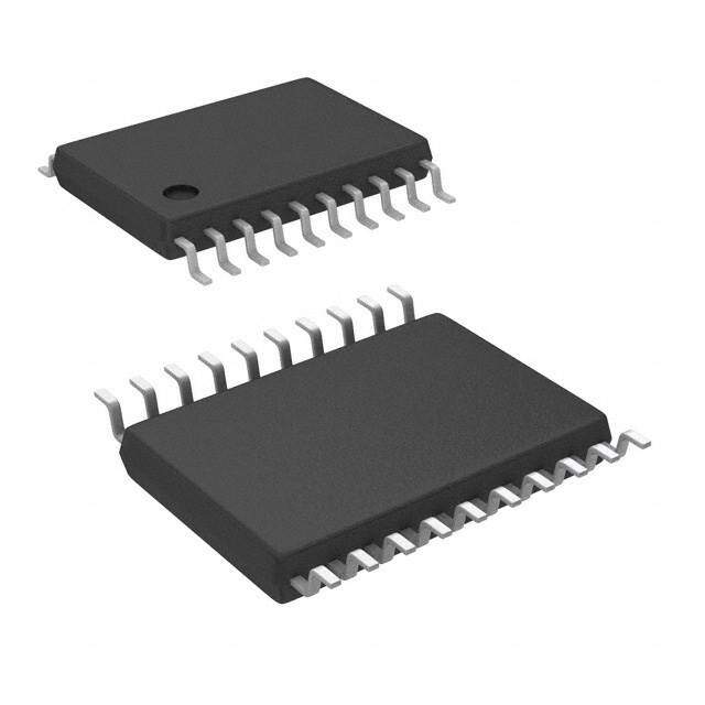
| 描述 | 时钟缓冲器 1-to-4 LVPECL Fanout Buffer |
| 产品分类 | 集成电路 - IC |
| 产品手册 | http://www.idt.com/document/dst/8533i-01-datasheet |
| 产品图片 |
|
| rohs | 符合RoHS |
| 产品系列 | 时钟和计时器IC,时钟缓冲器,IDT 8533AGI-01LF |
| 产品型号 | 8533AGI-01LF |
| 产品种类 | 时钟缓冲器 |
| 传播延迟—最大值 | 1.4 ns |
| 商标 | IDT |
| 安装风格 | SMD/SMT |
| 封装 | Tube |
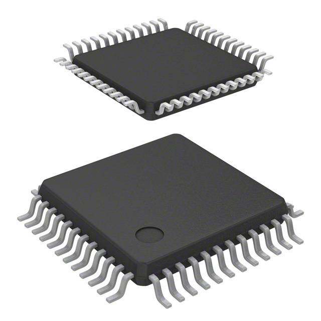
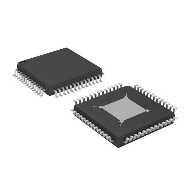
| 封装/箱体 | TSSOP-20 |
| 工厂包装数量 | 74 |
| 最大工作温度 | + 85 C |
| 最小工作温度 | - 40 C |
| 电源电压-最大 | 3.465 V |
| 电源电压-最小 | 3.135 V |
| 电源电流 | 50 mA |
| 系列 | 8533I-01 |
| 输出端数量 | 4 |
| 零件号别名 | 8533I-01 ICS8533AGI-01LF |


- 商务部:美国ITC正式对集成电路等产品启动337调查
- 曝三星4nm工艺存在良率问题 高通将骁龙8 Gen1或转产台积电
- 太阳诱电将投资9.5亿元在常州建新厂生产MLCC 预计2023年完工
- 英特尔发布欧洲新工厂建设计划 深化IDM 2.0 战略
- 台积电先进制程称霸业界 有大客户加持明年业绩稳了
- 达到5530亿美元!SIA预计今年全球半导体销售额将创下新高
- 英特尔拟将自动驾驶子公司Mobileye上市 估值或超500亿美元
- 三星加码芯片和SET,合并消费电子和移动部门,撤换高东真等 CEO
- 三星电子宣布重大人事变动 还合并消费电子和移动部门
- 海关总署:前11个月进口集成电路产品价值2.52万亿元 增长14.8%


PDF Datasheet 数据手册内容提取
Low Skew, 1-to-4 8533I-01 Differential-to-3.3V LVPECL Fanout Buffer DATA SHEET G D F ENERAL ESCRIPTION EATURES The 8533I-01 is a low skew, high performance 1-to-4 • Four differential 3.3V LVPECL outputs Differential-to-3.3V LVPECL Fanout Buffer. The 8533I-01 has • Selectable differential CLK, nCLK or LVPECL clock inputs two selectable clock inputs. The CLK, nCLK pair can accept most standard differential input levels. The PCLK, nPCLK pair • CLK, nCLK pair can accept the following differential can accept LVPECL, CML, or SSTL input levels. The clock input levels: LVDS, LVPECL, LVHSTL, SSTL, HCSL enable is internally synchronized to eliminate runt pulses on • PCLK, nPCLK supports the following input types: the outputs during asynchronous assertion/deassertion of the LVPECL, CML, SSTL clock enable pin. • Maximum output frequency: 650MHz Guaranteed output and part-to-part skew characteristics make the 8533I-01 ideal for those applications demanding well defi ned • Translates any single-ended input signal to 3.3V performance and repeatability. LVPECL levels with resistor bias on nCLK input • Output skew: 30ps (maximum) • Part-to-part skew: 150ps (maximum) • Propagation delay: 1.5ns (maximum), CLK/nCLK • Additive phase jitter, RMS: 0.060ps (typical) • 3.3V operating supply • -40°C to 85°C ambient operating temperature • Available in lead-free (RoHS 6) package B D P A LOCK IAGRAM IN SSIGNMENT 8533I-01 20-Lead TSSOP 6.5mm x 4.4mm x 0.92mm package body G Package Top View 8533I-01 REVISION A 7/9/15 1 ©2015 Integrated Device Technology, Inc.
8533I-01 DATA SHEET TABLE 1. PIN DESCRIPTIONS Number Name Type Description 1 V Power Negative supply pin. EE Synchronizing clock enable. When HIGH, clock outputs follow clock input. 2 CLK_EN Input Pullup When LOW, Q outputs are forced low, nQ outputs are forced high. LVC- MOS / LVTTL interface levels. Clock select input. When HIGH, selects differential PCLK, nPCLK inputs. 3 CLK_SEL Input Pulldown When LOW, selects CLK, nCLK inputs. LVCMOS / LVTTL interface levels. 4 CLK Input Pulldown Non-inverting differential clock input. 5 nCLK Input Pullup Inverting differential clock input. 6 PCLK Input Pulldown Non-inverting differential LVPECL clock input. 7 nPCLK Input Pullup Inverting differential LVPECL clock input. 8, 9 nc Unused No connect. 10, 13, 18 V Power Positive supply pins. CC 11, 12 nQ3, Q3 Output Differential output pair. LVPECL interface levels. 14, 15 nQ2, Q2 Output Differential output pair. LVPECL interface levels. 16, 17 nQ1, Q1 Output Differential output pair. LVPECL interface levels. 19, 20 nQ0, Q0 Output Differential output pair. LVPECL interface levels. NOTE: Pullup and Pulldown refer to internal input resistors. See Table 2, Pin Characteristics, for typical values. TABLE 2. PIN CHARACTERISTICS Symbol Parameter Test Conditions Minimum Typical Maximum Units C Input Capacitance 4 pF IN R Input Pullup Resistor 51 kΩ PULLUP R Input Pulldown Resistor 51 kΩ PULLDOWN LOW SKEW, 1-TO-4 2 REVISION A 7/9/15 DIFFERENTIAL-TO-3.3V LVPECL FANOUT BUFFER
8533I-01 DATA SHEET TABLE 3A. CONTROL INPUT FUNCTION TABLE Inputs Outputs CLK_EN CLK_SEL Selected Source Q0:Q3 nQ0:nQ3 0 0 CLK, nCLK Disabled; LOW Disabled; HIGH 0 1 PCLK, nPCLK Disabled; LOW Disabled; HIGH 1 0 CLK, nCLK Enabled Enabled 1 1 PCLK, nPCLK Enabled Enabled After CLK_EN switches, the clock outputs are disabled or enabled following a rising and falling input clock edge as shown in Figure 1. In the active mode, the state of the outputs are a function of the CLK , nCLK and PCLK, nPCLK inputs as described in Table 3B. FIGURE 1. CLK_EN TIMING DIAGRAM TABLE 3B. CLOCK INPUT FUNCTION TABLE Inputs Outputs Input to Output Mode Polarity CLK or PCLK nCLK or nPCLK Q0:Q3 nQ0:nQ3 0 1 LOW HIGH Differential to Differential Non Inverting 1 0 HIGH LOW Differential to Differential Non Inverting 0 Biased; NOTE 1 LOW HIGH Single Ended to Differential Non Inverting 1 Biased; NOTE 1 HIGH LOW Single Ended to Differential Non Inverting Biased; NOTE 1 0 HIGH LOW Single Ended to Differential Inverting Biased; NOTE 1 1 LOW HIGH Single Ended to Differential Inverting NOTE 1: Please refer to the Application Information section, “Wiring the Differential Input to Accept Single Ended Levels”. REVISION A 7/9/15 3 LOW SKEW, 1-TO-4 DIFFERENTIAL-TO-3.3V LVPECL FANOUT BUFFER
8533I-01 DATA SHEET ABSOLUTE MAXIMUM RATINGS Supply Voltage, V 4.6V CC NOTE: Stresses beyond those listed under Absolute Inputs, V -0.5V to V + 0.5V Maximum Ratings may cause permanent damage to the I CC Outputs, I device. These ratings are stress specifi cations only. Functional O Continuous Current 50mA operation of product at these conditions or any conditions Surge Current 100mA beyond those listed in the DC Characteristics or AC Charac- Package Thermal Impedance, θ 73.2°C/W (0 lfpm) teristics is not implied. Exposure to absolute maximum rating JA conditions for extended periods may affect product reliability. Storage Temperature, T -65°C to 150°C STG TABLE 4A. POWER SUPPLY DC CHARACTERISTICS, V = 3.3V±5%, TA = -40°C TO 85°C CC Symbol Parameter Test Conditions Minimum Typical Maximum Units V Positive Supply Voltage 3.135 3.3 3.465 V CC I Power Supply Current 52 mA EE TABLE 4B. LVCMOS / LVTTL DC CHARACTERISTICS, V = 3.3V±5%, TA = -40°C TO 85°C CC Symbol Parameter Test Conditions Minimum Typical Maximum Units V Input High Voltage 2 V + 0.3 V IH CC V Input Low Voltage -0.3 0.8 V IL CLK_EN V = V = 3.465V 5 µA I Input High Current IN CC IH CLK_SEL V = V = 3.465V 150 µA IN CC CLK_EN V = 0V, V = 3.465V -150 µA I Input Low Current IN CC IL CLK_SEL V = 0V, V = 3.465V -5 µA IN CC TABLE 4C. DIFFERENTIAL DC CHARACTERISTICS, V = 3.3V±5%, TA = -40°C TO 85°C CC Symbol Parameter Test Conditions Minimum Typical Maximum Units nCLK V = V = 3.465V 5 µA I Input High Current CC IN IH CLK V = V = 3.465V 150 µA CC IN nCLK V = 3.465V, V = 0V -150 µA I Input Low Current CC IN IL CLK V = 3.465V, V = 0V -5 µA CC IN V Peak-to-Peak Input Voltage 0.15 1.3 V PP Common Mode Input Voltage; V V + 0.5 V - 0.85 V CMR NOTE 1, 2 EE CC NOTE 1: For single ended applications, the maximum input voltage for CLK and nCLK is V + 0.3V. CC NOTE 2: Common mode voltage is defi ned as V . IH LOW SKEW, 1-TO-4 4 REVISION A 7/9/15 DIFFERENTIAL-TO-3.3V LVPECL FANOUT BUFFER
8533I-01 DATA SHEET TABLE 4D. LVPECL DC CHARACTERISTICS, V = 3.3V±5%, TA = -40°C TO 85°C CC Symbol Parameter Test Conditions Minimum Typical Maximum Units PCLK V = V = 3.465V 150 µA I Input High Current CC IN IH nPCLK V = V = 3.465V 5 µA CC IN PCLK V = 3.465V, V = 0V -5 µA I Input Low Current CC IN IL nPCLK V = 3.465V, V = 0V -150 µA CC IN V Peak-to-Peak Input Voltage 0.3 1 V PP V Common Mode Input Voltage; NOTE 1, 2 V + 1.5 V V CMR EE CC V Output High Voltage; NOTE 3 V - 1.4 V - 0.9 V OH CC CC V Output Low Voltage; NOTE 3 V - 2.0 V - 1.7 V OL CC CC V Peak-to-Peak Output Voltage Swing 0.6 1.0 V SWING NOTE 1: Common mode voltage is defi ned as V . IH NOTE 2: For single ended applications the maximum input voltage for PCLK and nPCLK is V + 0.3V. NOTE 3: Outputs terminated with 50Ω to V - 2V. CC CC TABLE 5. AC CHARACTERISTICS, V = 3.3V±5%, TA = -40°C TO 85°C CC Symbol Parameter Test Conditions Minimum Typical Maximum Units f Output Frequency 650 MHz MAX Propagation Delay; CLK, nCLK 1.15 1.5 ns t PD NOTE 1 PCLK, nPCLK 1.0 1.3 ns tsk(o) Output Skew; NOTE 2, 4 30 ps tsk(pp) Part-to-Part Skew; NOTE 3, 4 150 ps Buffer Additive Phase Jitter, RMS; tjit 0.060 ps refer to Additive Phase Jitter section t / t Output Rise/Fall Time 300 800 ps R F odc Output Duty Cycle 47 53 % All parameters measured at f £ 650MHz unless noted otherwise. The cycle to cycle jitter on the input will equal the jitter on the output. The part does not add jitter. NOTE 1: Measured from the differential input crossing point to the differential output crossing point. NOTE 2: Defi ned as skew between outputs at the same supply voltage and with equal load conditions. Measured at output differential cross points. NOTE 3: Defi ned as skew between outputs on different devices operating at the same supply voltages and with equal load conditions. Using the same type of inputs on each device, the outputs are measured at the differential cross points. NOTE 4: This parameter is defi ned in accordance with JEDEC Standard 65. REVISION A 7/9/15 5 LOW SKEW, 1-TO-4 DIFFERENTIAL-TO-3.3V LVPECL FANOUT BUFFER
8533I-01 DATA SHEET A P J DDITIVE HASE ITTER The spectral purity in a band at a specifi c offset from the the 1Hz band to the power in the fundamental. When the required fundamental compared to the power of the fundamental is offset is specifi ed, the phase noise is called a dBc value, which called the dBc Phase Noise. This value is normally expressed simply means dBm at a specifi ed offset from the fundamental. using a Phase noise plot and is most often the specifi ed plot By investigating jitter in the frequency domain, we get a better in many applications. Phase noise is defi ned as the ratio of the understanding of its effects on the desired application over the noise power present in a 1Hz band at a specifi ed offset from the entire time record of the signal. It is mathematically possible to fundamental frequency to the power value of the fundamental. calculate an expected bit error rate given a phase noise plot. This ratio is expressed in decibels (dBm) or a ratio of the power in 0 -10 Input/Output Additive -20 Phase Jitter at 156.25MHz = 0.060ps (typical) -30 -40 -50 -60 Z H c/ -70 B d -80 E S OI -90 N E -100 S A PH -110 B S -120 S -130 -140 -150 -160 -170 -180 -190 1k 10k 100k 1M 10M 100M OFFSET FROM CARRIER FREQUENCY (HZ) As with most timing specifi cations, phase noise measurements device meets the noise fl oor of what is shown, but can actually have issues. The primary issue relates to the limitations of the be lower. The phase noise is dependent on the input source and equipment. Often the noise fl oor of the equipment is higher measurement equipment. than the noise fl oor of the device. This is illustrated above. The LOW SKEW, 1-TO-4 6 REVISION A 7/9/15 DIFFERENTIAL-TO-3.3V LVPECL FANOUT BUFFER
8533I-01 DATA SHEET P M I ARAMETER EASUREMENT NFORMATION 3.3V OUTPUT LOAD AC TEST CIRCUIT DIFFERENTIAL INPUT LEVEL OUTPUT SKEW PROPAGATION DELAY OUTPUT RISE/FALL TIME OUTPUT DUTY CYCLE/PULSE WIDTH/PERIOD REVISION A 7/9/15 7 LOW SKEW, 1-TO-4 DIFFERENTIAL-TO-3.3V LVPECL FANOUT BUFFER
8533I-01 DATA SHEET A I PPLICATION NFORMATION WIRING THE DIFFERENTIAL INPUT TO ACCEPT SINGLE ENDED LEVELS Figure 2 shows how the differential input can be wired to accept of R1 and R2 might need to be adjusted to position the V_REF single ended levels. The reference voltage V_REF = V /2 is in the center of the input voltage swing. For example, if the input CC generated by the bias resistors R1, R2 and C1. This bias circuit clock swing is only 2.5V and V = 3.3V, V_REF should be 1.25V CC should be located as close as possible to the input pin. The ratio and R2/R1 = 0.609. FIGURE 2. SINGLE ENDED SIGNAL DRIVING DIFFERENTIAL INPUT RECOMMENDATIONS FOR UNUSED INPUT AND OUTPUT PINS INPUTS: OUTPUTS: CLK/nCLK INPUT: LVPECL OUTPUT For applications not requiring the use of the differential input, All unused LVPECL outputs can be left fl oating. We recommend both CLK and nCLK can be left fl oating. Though not required, that there is no trace attached. Both sides of the differential but for additional protection, a 1kΩ resistor can be tied from output pair should either be left fl oating or terminated. CLK to ground. PCLK/nPCLK INPUT: For applications not requiring the use of a differential input, both the PCLK and nPCLK pins can be left fl oating. Though not required, but for additional protection, a 1kΩ resistor can be tied from PCLK to ground. LVCMOS CONTROL PINS: All control pins have internal pull-ups or pull-downs; additional resistance is not required but can be added for additional protection. A 1kΩ resistor can be used. LOW SKEW, 1-TO-4 8 REVISION A 7/9/15 DIFFERENTIAL-TO-3.3V LVPECL FANOUT BUFFER
8533I-01 DATA SHEET DIFFERENTIAL CLOCK INPUT INTERFACE The CLK /nCLK accepts LVDS, LVPECL, LVHSTL, SSTL, vendor of the driver component to confi rm the driver termination HCSL and other differential signals. Both VSWING and VOH must requirements. For example in Figure 3A, the input termination meet the VPP and VCMR input requirements. Figures 3A to 3E applies for ICS HiPerClockS LVHSTL drivers. If you are using show interface examples for the HiPerClockS CLK/nCLK input an LVHSTL driver from another vendor, use their termination driven by the most common driver types. The input interfaces recommendation. suggested here are examples only. Please consult with the 3.3V 3.3V 3.3V 1.8V Zo = 50 Ohm Zo = 50 Ohm CLK CLK Zo = 50 Ohm Zo = 50 Ohm nCLK HiPerClockS LVPECL Input nCLK HiPerClockS LVHSTL Input R1 R2 50 50 ICS R1 R2 HiPerClockS 50 50 LVHSTL Driver R3 50 FIGURE 3A. HIPERCLOCKS CLK/NCLK INPUT DRIVEN BY FIGURE 3B. HIPERCLOCKS CLK/NCLK INPUT DRIVEN BY ICS HIPERCLOCKS LVHSTL DRIVER 3.3V LVPECL DRIVER 3.3V 3.3V 3.3V 3.3V 3.3V Zo = 50 Ohm R3 R4 125 125 Zo = 50 Ohm LVDS_Driver CLK CLK Zo = 50 Ohm R1 100 nCLK HiPerClockS nCLK Receiver LVPECL Input Zo = 50 Ohm R1 R2 84 84 FIGURE 3C. HIPERCLOCKS CLK/NCLK INPUT DRIVEN BY FIGURE 3D. HIPERCLOCKS CLK/NCLK INPUT DRIVEN BY 3.3V LVPECL DRIVER 3.3V LVDS DRIVER 3.3V 3.3V 3.3V R3 R4 125 125 LVPECL Zo = 50 Ohm C1 CLK Zo = 50 Ohm C2 nCLK HiPerClockS Input R5 R6 R1 R2 100 - 200 100 - 200 84 84 R5,R6 locate near the driver pin. FIGURE 3E. HIPERCLOCKS CLK/NCLK INPUT DRIVEN BY 3.3V LVPECL DRIVER WITH AC COUPLE REVISION A 7/9/15 9 LOW SKEW, 1-TO-4 DIFFERENTIAL-TO-3.3V LVPECL FANOUT BUFFER
8533I-01 DATA SHEET LVPECL CLOCK INPUT INTERFACE The PCLK /nPCLK accepts LVPECL, CML, SSTL and other dif- only. If the driver is from another vendor, use their termination ferential signals. Both VSWING and VOH must meet the VPP and VCMR recommendation. Please consult with the vendor of the driver input requirements. Figures 4A to 4F show interface examples for component to confi rm the driver termination requirements. the HiPerClockS PCLK/nPCLK input driven by the most common driver types. The input interfaces suggested here are examples 3.3V 3.3V 3.3V R1 R2 50 50 CML Zo = 50 Ohm PCLK Zo = 50 Ohm nPCLK HiPerClockS PCLK/nPCLK FIGURE 4A. HIPERCLOCKS PCLK/nPCLK INPUT DRIVEN FIGURE 4B. HIPERCLOCKS PCLK/nPCLK INPUT DRIVEN BY AN OPEN COLLECTOR CML DRIVER BY A BUILT-IN PULLUP CML DRIVER 3.3V 3.3V 3.3V 3.3V 3.3V R1235 R1245 3.3V 3.3V LVPECL Zo = 50 Ohm C1 R843 R844 Zo = 50 Ohm PCLK PCLK Zo = 50 Ohm C2 Zo = 50 Ohm nPCLK HiPerClockS nPCLK HiPerClockS PCLK/nPCLK LVPECL Input R5 R6 R1 R2 100 - 200 100 - 200 125 125 R1 R2 84 84 FIGURE 4C. HIPERCLOCKS PCLK/nPCLK INPUT DRIVEN FIGURE 4D. HIPERCLOCKS PCLK/nPCLK INPUT DRIVEN BY A 3.3V LVPECL DRIVER BY A 3.3V LVPECL DRIVER WITH AC COUPLE 2.5V 3.3V 2.5V SSTL Zo = 60 Ohm R1230 R1240 3.3V 3.3V LVDS Zo = 50 Ohm C1 R1K3 R1K4 3.3V PCLK PCLK Zo = 60 Ohm R1050 C2 nPCLK PHCiPLeKrC/nloPcCkLSK Zo = 50 Ohm nPCLK HPCiPLeKrC/nloPcCkSLK R1210 R1220 R1K1 R1K2 FIGURE 4E. HIPERCLOCKS PCLK/nPCLK INPUT DRIVEN FIGURE 4F. HIPERCLOCKS PCLK/nPCLK INPUT DRIVEN BY AN SSTL DRIVER BY A 3.3V LVDS DRIVER LOW SKEW, 1-TO-4 10 REVISION A 7/9/15 DIFFERENTIAL-TO-3.3V LVPECL FANOUT BUFFER
8533I-01 DATA SHEET TERMINATION FOR LVPECL OUTPUTS The clock layout topology shown below is a typical termination techniques should be used to maximize operating frequency for LVPECL outputs. The two different layouts mentioned are and minimize signal distortion. Figures 5A and 5B show two recommended only as guidelines. different layouts which are recommended only as guidelines. Other suitable clock layouts may exist and it would be FOUT and nFOUT are low impedance follower outputs recommended that the board designers simulate to guarantee that generate ECL/LVPECL compatible outputs. Therefore, compatibility across all printed circuit and clock component terminating resistors (DC current path to ground) or current process variations. sources must be used for functionality. These outputs are designed to drive 50Ω transmission lines. Matched impedance FIGURE 5A. LVPECL OUTPUT TERMINATION FIGURE 5B. LVPECL OUTPUT TERMINATION REVISION A 7/9/15 11 LOW SKEW, 1-TO-4 DIFFERENTIAL-TO-3.3V LVPECL FANOUT BUFFER
8533I-01 DATA SHEET P C OWER ONSIDERATIONS This section provides information on power dissipation and junction temperature for the 8533I-01. Equations and example calculations are also provided. 1. Power Dissipation. The total power dissipation for the 8533I-01 is the sum of the core power plus the power dissipated in the load(s). The following is the power dissipation for V = 3.3V + 5% = 3.465V, which gives worst case results. CC NOTE: Please refer to Section 3 for details on calculating power dissipated in the load. • Power (core) = V * I = 3.465V * 52mA = 180.2mW MAX CC_MAX EE_MAX • Power (outputs) = 30mW/Loaded Output pair MAX If all outputs are loaded, the total power is 4 * 30mW = 120mW Total Power (3.465V, with all outputs switching) = 180.2mW + 120mW = 300.2mW _MAX 2. Junction Temperature. Junction temperature, Tj, is the temperature at the junction of the bond wire and bond pad and directly affects the reliability of the device. The maximum recommended junction temperature for HiPerClockSTM devices is 125°C. The equation for Tj is as follows: Tj = θJA * Pd_total + TA Tj = Junction Temperature θJA = Junction-to-Ambient Thermal Resistance Pd_total = Total Device Power Dissipation (example calculation is in section 1 above) TA = Ambient Temperature In order to calculate junction temperature, the appropriate junction-to-ambient thermal resistance θJAmust be used. Assuming a moderate air fl ow of 200 linear feet per minute and a multi-layer board, the appropriate value is 66.6°C/W per Table 6 below. Therefore, Tj for an ambient temperature of 85°C with all outputs switching is: 85°C + 0.300W * 66.6°C/W = 105°C. This is well below the limit of 125°C. This calculation is only an example. Tj will obviously vary depending on the number of loaded outputs, supply voltage, air fl ow, and the type of board (single layer or multi-layer). TABLE 6. THERMAL RESISTANCE θJA FOR 20-PIN TSSOP, FORCED CONVECTION θ by Velocity (Linear Feet per Minute) JA 0 200 500 Single-Layer PCB, JEDEC Standard Test Boards 114.5°C/W 98.0°C/W 88.0°C/W Multi-Layer PCB, JEDEC Standard Test Boards 73.2°C/W 66.6°C/W 63.5°C/W NOTE: Most modern PCB designs use multi-layered boards. The data in the second row pertains to most designs. LOW SKEW, 1-TO-4 12 REVISION A 7/9/15 DIFFERENTIAL-TO-3.3V LVPECL FANOUT BUFFER
8533I-01 DATA SHEET 3. Calculations and Equations. The purpose of this section is to derive the power dissipated into the load. LVPECL output driver circuit and termination are shown in Figure 6. FIGURE 6. LVPECL DRIVER CIRCUIT AND TERMINATION To calculate worst case power dissipation into the load, use the following equations which assume a 50Ω load, and a termination voltage of V - 2V. CC • For logic high, V = V = V – 0.9V OUT OH_MAX CC_MAX (V - V ) = 0.9V CC_MAX OH_MAX • For logic low, V = V = V – 1.7V OUT OL_MAX CC_MAX (V - V ) = 1.7V CC_MAX OL_MAX Pd_H is power dissipation when the output drives high. Pd_L is the power dissipation when the output drives low. Pd_H = [(V – (V - 2V))/R] * (V - V ) = [(2V - (V - V ))/R] * (V - V ) = OH_MAX CC_MAX L CC_MAX OH_MAX CC_MAX OH_MAX L CC_MAX OH_MAX [(2V - 0.9V)/50Ω] * 0.9V = 19.8mW Pd_L = [(V – (V - 2V))/R] * (V - V ) = [(2V - (V - V ))/R] * (V - V ) = OL_MAX CC_MAX L CC_MAX OL_MAX CC_MAX OL_MAX L CC_MAX OL_MAX [(2V - 1.7V)/50Ω] * 1.7V = 10.2mW Total Power Dissipation per output pair = Pd_H + Pd_L = 30mW REVISION A 7/9/15 13 LOW SKEW, 1-TO-4 DIFFERENTIAL-TO-3.3V LVPECL FANOUT BUFFER
8533I-01 DATA SHEET R I ELIABILITY NFORMATION θ TABLE 7. VS. AIR FLOW TABLE FOR 20 LEAD TSSOP JA θ by Velocity (Linear Feet per Minute) JA 0 200 500 Single-Layer PCB, JEDEC Standard Test Boards 114.5°C/W 98.0°C/W 88.0°C/W Multi-Layer PCB, JEDEC Standard Test Boards 73.2°C/W 66.6°C/W 63.5°C/W NOTE: Most modern PCB designs use multi-layered boards. The data in the second row pertains to most designs. TRANSISTOR COUNT The transistor count for 8533I-01 is: 404 LOW SKEW, 1-TO-4 14 REVISION A 7/9/15 DIFFERENTIAL-TO-3.3V LVPECL FANOUT BUFFER
8533I-01 DATA SHEET PACKAGE OUTLINE - G SUFFIX FOR 20 LEAD TSSOP TABLE 8. PACKAGE DIMENSIONS Millimeters SYMBOL Minimum Maximum N 20 A -- 1.20 A1 0.05 0.15 A2 0.80 1.05 b 0.19 0.30 c 0.09 0.20 D 6.40 6.60 E 6.40 BASIC E1 4.30 4.50 e 0.65 BASIC L 0.45 0.75 α 0° 8° aaa -- 0.10 Reference Document: JEDEC Publication 95, MS-153 REVISION A 7/9/15 15 LOW SKEW, 1-TO-4 DIFFERENTIAL-TO-3.3V LVPECL FANOUT BUFFER
8533I-01 DATA SHEET TABLE 9. ORDERING INFORMATION Part/Order Number Marking Package Shipping Packaging Temperature 8533AGI-01LF 8533AI01L 20 lead “Lead Free” TSSOP tube -40°C to 85°C 8533AGI-01LFT 8533AI01L 20 lead “Lead Free” TSSOP tape & reel -40°C to 85°C NOTE: Parts that are ordered with an “LF” suffi x to the part number are the Pb-Free confi guration and are RoHS compliant. LOW SKEW, 1-TO-4 16 REVISION A 7/9/15 DIFFERENTIAL-TO-3.3V LVPECL FANOUT BUFFER
8533I-01 DATA SHEET REVISION HISTORY SHEET Rev Table Page Description of Change Date 1 Features Section - added lead-free note. 8 Added Recommendations for Unused Input and Output Pins. A 4/21/06 T9 10 Updated LVPECL Clock Input Interface. 16 Ordering Information Table - added lead-free part number, marking and note. A T9 16 Ordering Information Table - Changed non lead free marking 12-6-07 T9 16 Ordering Information Table - removed leaded devices. A 7/9/15 Updated data sheet format. REVISION A 7/9/15 17 LOW SKEW, 1-TO-4 DIFFERENTIAL-TO-3.3V LVPECL FANOUT BUFFER
Corporate Headquarters Sales Technical Support 6024 Silver Creek Valley Road 800-345-7015 or +408-284-8200 email: clocks@idt.com Fax: 408-284-2775 San Jose, California 95138 www.IDT.com DISCLAIMER Integrated Device Technology, Inc. (IDT) and its subsidiaries reserve the right to modify the products and/or specifi cations described herein at any time and at IDT’s sole discretion. All information in this document, including descriptions of product features and performance, is subject to change without notice. Performance specifi cations and the operating parameters of the described products are determined in the independent state and are not guaranteed to perform the same way when installed in customer products. The information contained herein is provided without representation or warranty of any kind, wheth- er express or implied, including, but not limited to, the suitability of IDT’s products for any particular purpose, an implied warranty of merchantability, or non-infringement of the intellectual property rights of others. This document is presented only as a guide and does not convey any license under intellectual property rights of IDT or any third parties. IDT’s products are not intended for use in applications involving extreme environmental conditions or in life support systems or similar devices where the failure or malfunction of an IDT product can be reason- ably expected to signifi cantly affect the health or safety of users. Anyone using an IDT product in such a manner does so at their own risk, absent an express, written agreement by IDT. Integrated Device Technology, IDT and the IDT logo are registered trademarks of IDT. Other trademarks and service marks used herein, including protected names, logos and designs, are the property of IDT or their respective third party owners. Copyright 2015. All rights reserved.
Mouser Electronics Authorized Distributor Click to View Pricing, Inventory, Delivery & Lifecycle Information: I DT (Integrated Device Technology): 8533AGI-01LF 8533AGI-01LFT