ICGOO在线商城 > 8304AMI

 Datasheet下载
- 型号: 8304AMI
- 制造商: Integrated Device Technology
- 库位|库存: xxxx|xxxx
- 要求:
| 数量阶梯 | 香港交货 | 国内含税 |
| +xxxx | $xxxx | ¥xxxx |
查看当月历史价格
查看今年历史价格
8304AMI产品简介:
ICGOO电子元器件商城为您提供8304AMI由Integrated Device Technology设计生产,在icgoo商城现货销售,并且可以通过原厂、代理商等渠道进行代购。 提供8304AMI价格参考以及Integrated Device Technology8304AMI封装/规格参数等产品信息。 你可以下载8304AMI参考资料、Datasheet数据手册功能说明书, 资料中有8304AMI详细功能的应用电路图电压和使用方法及教程。
| 参数 | 数值 |
| 品牌 | IDT |
| 产品目录 | 半导体 |
| 描述 | 时钟缓冲器 1-to-4 LVCMOS Fanout Buffer |
| 产品分类 | 集成电路 - IC |
| 产品手册 | http://www.idt.com/document/8304i-datasheet-0 |
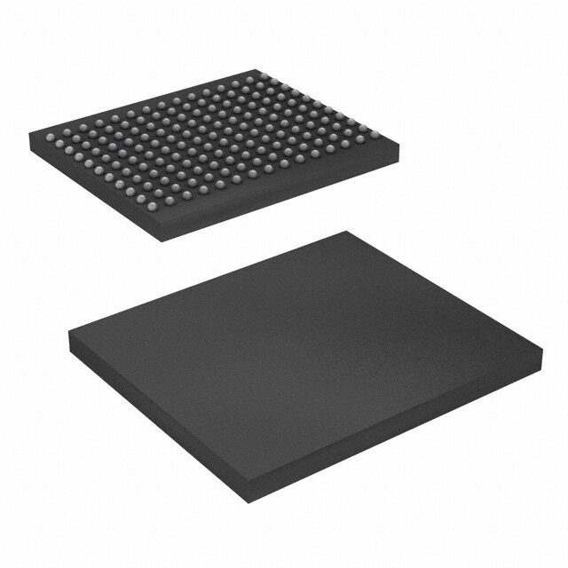
| 产品图片 |
|
| rohs | 否 |
| 产品系列 | 时钟和计时器IC,时钟缓冲器,IDT 8304AMI |
| 产品型号 | 8304AMI |
| 产品种类 | 时钟缓冲器 |
| 传播延迟—最大值 | 3.7 ns |
| 商标 | IDT |
| 安装风格 | SMD/SMT |
| 封装 | Tray |
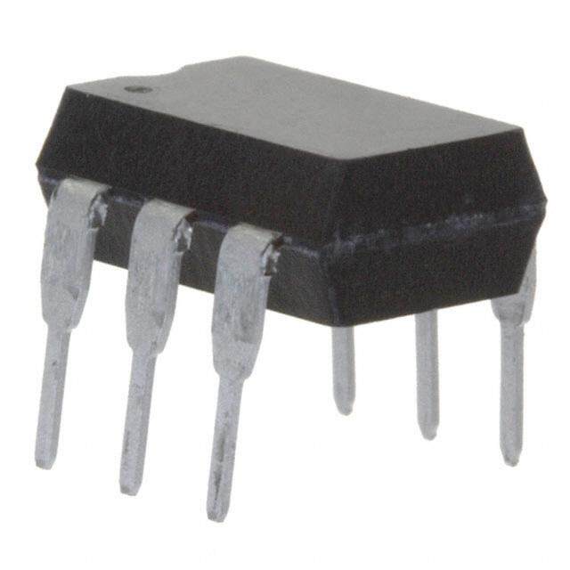
| 封装/箱体 | SOIC-8 |
| 工厂包装数量 | 97 |
| 最大工作温度 | + 85 C |
| 最大输出频率 | 166 MHz |
| 最小工作温度 | - 40 C |
| 电源电压-最大 | 3.465 V |
| 电源电压-最小 | 3.135 V |
| 电源电流 | 18 mA |
| 输入类型 | LVCMOS |
| 输出端数量 | 4 |
| 输出类型 | LVCMOS,LVTTL |
| 零件号别名 | ICS8304AMI |


- 商务部:美国ITC正式对集成电路等产品启动337调查
- 曝三星4nm工艺存在良率问题 高通将骁龙8 Gen1或转产台积电
- 太阳诱电将投资9.5亿元在常州建新厂生产MLCC 预计2023年完工
- 英特尔发布欧洲新工厂建设计划 深化IDM 2.0 战略
- 台积电先进制程称霸业界 有大客户加持明年业绩稳了
- 达到5530亿美元!SIA预计今年全球半导体销售额将创下新高
- 英特尔拟将自动驾驶子公司Mobileye上市 估值或超500亿美元
- 三星加码芯片和SET,合并消费电子和移动部门,撤换高东真等 CEO
- 三星电子宣布重大人事变动 还合并消费电子和移动部门
- 海关总署:前11个月进口集成电路产品价值2.52万亿元 增长14.8%


PDF Datasheet 数据手册内容提取
Low Skew, 1-to-4 LVCMOS/LVTTL 8304I Fanout Buffer Data Sheet G D F ENERAL ESCRIPTION EATURES The 8304I is a low skew, 1-to-4 Fanout Buffer. The 8304I is charac- • Four LVCMOS / LVTTL outputs terized at full 3.3V for input V , and mixed 3.3V and 2.5V for output DD • LVCMOS clock input operating supply modes (V ). Guaranteed output and part-to-part skew characteristics make thDDeO 8304I ideal for those clock distribution • CLK can accept the following input levels: LVCMOS, LVTTL applications demanding well defi ned performance and repeatability. • Maximum output frequency: 166MHz • Output skew: 60ps (maximum) • Part-to-part skew: 650ps (maximum) • Small 8 lead SOIC package saves board space • 3.3V input, outputs may be either 3.3V or 2.5V supply modes • -40°C to 85°C ambient operating temperature • Available in lead-free (RoHS 6) compliant package B D P A LOCK IAGRAM IN SSIGNMENT Q0 VDDO 1 8 Q3 VDD 2 7 Q2 Q1 CLK 3 6 Q1 CLK Pulldown GND 4 5 Q0 Q2 8304I 8-Lead SOIC Q3 3.8mm x 4.8mm, x 1.47mm package body M Package Top View ©2015 Integrated Device Technology, Inc 1 December 10, 2015
8304I Data Sheet TABLE 1. PIN DESCRIPTIONS Number Name Type Description 1 V Power Output supply pin. Connect to 3.3V or 2.5V. DDO 2 V Power Positive supply pin. Connect to 3.3V. DD 3 CLK Input Pulldown LVCMOS / LVTTL clock input. 4 GND Power Power supply ground. Connect to ground. 5 Q0 Output Single clock output. LVCMOS / LVTTL interface levels. 6 Q1 Output Single clock output. LVCMOS / LVTTL interface levels. 7 Q2 Output Single clock output. LVCMOS / LVTTL interface levels. 8 Q3 Output Single clock output. LVCMOS / LVTTL interface levels. NOTE: Pulldown refer to internal input resistors. See Table 2, Pin Characteristics, for typical values. TABLE 2. PIN CHARACTERISTICS Symbol Parameter Test Conditions Minimum Typical Maximum Units C Input Capacitance 4 pF IN Power Dissipation Capacitance C V , V = 3.465V 15 pF PD (per output) DD DDO R Input Pulldown Resistor 51 kΩ PULLDOWN R Output Impedance 7 Ω OUT ©2015 Integrated Device Technology, Inc 2 December 10, 2015
8304I Data Sheet ABSOLUTE MAXIMUM RATINGS Supply Voltage, V 4.6V DD NOTE: Stresses beyond those listed under Absolute Inputs, V -0.5V to V + 0.5 V Maximum Ratings may cause permanent damage to the I DD device. These ratings are stress specifi cations only. Functional Outputs, V -0.5V to V + 0.5V O DDO operation of product at these conditions or any conditions beyond Package Thermal Impedance, θ 112.7°C/W (0 lfpm) those listed in the DC Characteristics or AC Characteristics is not JA implied. Exposure to absolute maximum rating conditions for ex- Storage Temperature, T -65°C to 150°C STG tended periods may affect product reliability. TABLE 3A. POWER SUPPLY DC CHARACTERISTICS, V = V = 3.3V±5%, TA = -40°C TO 85°C DD DDO Symbol Parameter Test Conditions Minimum Typical Maximum Units V Power Supply Voltage 3.135 3.3 3.465 V DD V Output Power Supply Voltage 3.135 3.3 3.465 V DDO I Power Supply Current 18 mA DD I Output Supply Current 11 mA DDO TABLE 3B. POWER SUPPLY DC CHARACTERISTICS, V = 3.3V±5%, V = 2.5V±5%, TA = -40°C TO 85°C DD DDO Symbol Parameter Test Conditions Minimum Typical Maximum Units V Positive Supply Voltage 3.135 3.3 3.465 V DD V Output Supply Voltage 2.375 2.5 2.625 V DDO I Power Supply Current 18 mA DD I Output Supply Current 11 mA DDO TABLE 3C. LVCMOS / LVTTL DC CHARACTERISTICS, V = V = 3.3V±5%, TA = -40°C TO 85°C DD DDO Symbol Parameter Test Conditions Minimum Typical Maximum Units V Input High Voltage 2 V + 0.3 V IH DD V Input Low Voltage -0.3 1.3 V IL I Input High Current V = V = 3.465V 150 µA IH DD IN I Input Low Current V = 3.465V, V = 0V -5 µA IL DD IN Refer to NOTE 1 2.6 V V Output High Voltage I = -16mA 2.9 V OH OH I = -100uA 3 V OH Refer to NOTE 1 0.5 V V Output Low Voltage I = 16mA 0.25 V OL OL I = 100uA 0.15 V OL NOTE 1: Outputs terminated with 50Ω to V /2. See Parameter Measurement Section, “3.3V Output Load Test Circuit”. Ω DDO ©2015 Integrated Device Technology, Inc 3 December 10, 2015
8304I Data Sheet TABLE 3D. LVCMOS / LVTTL DC CHARACTERISTICS, V = 3.3V±5%, V = 2.5V±5%, TA = -40°C TO 85°C DD DDO Symbol Parameter Test Conditions Minimum Typical Maximum Units V Input High Voltage 2 V + 0.3 V IH DD V Input Low Voltage -0.3 1.3 V IL I Input High Current V = V = 3.465V 150 µA IH DD IN I Input Low Current V = 3.465V, V = 0V -5 µA IL DD IN V Output High Voltage; NOTE 1 2.1 V OH V Output Low Voltage; NOTE 1 0.5 V OL NOTE 1: Outputs terminated with 50Ω to V /2. See Parameter Measurement Section, “3.3V/2.5V Output Load Test Circuit”. ΩΩΩ DDO TABLE 4A. AC CHARACTERISTICS, V = V = 3.3V±5%, TA = -40°C TO 85°C DD DDO Symbol Parameter Test Conditions Minimum Typical Maximum Units f Output Frequency 166 MHz MAX Propagation Delay, tp ƒ ≤ 166MHz 2 3.3 ns LH Low-to-High; NOTE 1 125MHz, Buffer Additive Phase Jitter, RMS; tjit Integration Range 0.17 ps refer to Additive Phase Jitter Section 12kHz – 20MHz tsk(o) Output Skew; NOTE 2, 4 ƒ = 133MHz 50 ps tsk(pp) Part-to-Part Skew; NOTE 3, 4 600 ps t Output Rise Time 30% to 70% 250 500 ps R t Output Fall Time 30% to 70% 250 500 ps F odc Output Duty Cycle 40 60 % NOTE: Electrical parameters are guaranteed over the specifi ed ambient operating temperature range, which is established when the device is mounted in a test socket with maintained transverse airfl ow greater than 500 lfpm. The device will meet specifi cations after thermal equilibrium has been reached under these conditions. NOTE: All parameters measured at 166MHz unless noted otherwise. NOTE 1: Measured from V /2 of the input to V /2 of the output. DD DDO NOTE 2: Defi ned as skew between outputs at the same supply voltage and with equal load conditions. Measured at V /2. DDO NOTE 3: Defi ned as skew between outputs on different devices operating at the same supply voltages and with equal load conditions. Using the same type of inputs on each device, the outputs are measured at V /2. DDO NOTE 4: This parameter is defi ned in accordance with JEDEC Standard 65. ©2015 Integrated Device Technology, Inc 4 December 10, 2015
8304I Data Sheet TABLE 4B. AC CHARACTERISTICS, V = 3.3V±5%, V = 2.5V±5%, TA = -40°C TO 85°C DD DDO Symbol Parameter Test Conditions Minimum Typical Maximum Units f Output Frequency 166 MHz MAX tp Propagation Delay, Low-to-High; NOTE 1 ƒ ≤ 166MHz 2.3 3.7 ns LH tsk(o) Output Skew; NOTE 2, 4 ƒ = 133MHz 60 ps tsk(pp) Part-to-Part Skew; NOTE 3, 4 650 ps t Output Rise Time 30% to 70% 250 500 ps R t Output Fall Time 30% to 70% 250 500 ps F odc Output Duty Cycle 40 60 % NOTE: Electrical parameters are guaranteed over the specifi ed ambient operating temperature range, which is established when the device is mounted in a test socket with maintained transverse airfl ow greater than 500 lfpm. The device will meet specifi cations after thermal equilibrium has been reached under these conditions. All parameters measured at 166MHz unless noted otherwise. NOTE 1: Measured from V /2 of the input to V /2 of the output. DD DDO NOTE 2: Defi ned as skew between outputs at the same supply voltage and with equal load conditions. Measured at V /2. DDO NOTE 3: Defi ned as skew between outputs on different devices operating at the same supply voltages and with equal load conditions. Using the same type of inputs on each device, the outputs are measured at V /2. DDO NOTE 4: This parameter is defi ned in accordance with JEDEC Standard 65. ©2015 Integrated Device Technology, Inc 5 December 10, 2015
8304I Data Sheet A P J DDITIVE HASE ITTER The spectral purity in a band at a specifi c offset from the fundamental (dBm) or a ratio of the power in the 1Hz band to the power in the compared to the power of the fundamental is called the dBc Phase fundamental. When the required offset is specifi ed, the phase noise Noise. This value is normally expressed using a Phase noise plot is called a dBc value, which simply means dBm at a specifi ed offset and is most often the specifi ed plot in many applications. Phase from the fundamental. By investigating jitter in the frequency domain, noise is defi ned as the ratio of the noise power present in a 1Hz we get a better understanding of its effects on the desired application band at a specifi ed offset from the fundamental frequency to the over the entire time record of the signal. It is mathematically possible power value of the fundamental. This ratio is expressed in decibels to calculate an expected bit error rate given a phase noise plot. Additive Phase Jitter @ 125MHz (12kHz to 20MHz) = 0.17ps typical As with most timing specifi cations, phase noise measurements has This is illustrated above. The device meets the noise fl oor of what issues relating to the limitations of the equipment. Often the noise is shown, but can actually be lower. The phase noise is dependent fl oor of the equipment is higher than the noise fl oor of the device. on the input source and measurement equipment. ©2015 Integrated Device Technology, Inc 6 December 10, 2015
8304I Data Sheet P M I ARAMETER EASUREMENT NFORMATION 3.3V OUTPUT LOAD AC TEST CIRCUIT 2.5V OUTPUT LOAD AC TEST CIRCUIT OUTPUT SKEW PART-TO-PART SKEW OUTPUT RISE/FALL TIME OUTPUT DUTY CYCLE/PULSE WIDTH/PERIOD PROPAGATION DELAY ©2015 Integrated Device Technology, Inc 7 December 10, 2015
8304I Data Sheet R I ELIABILITY NFORMATION θ TABLE 5. VS. AIR FLOW TABLE JA θ by Velocity (Linear Feet per Minute) JA 0 200 500 Single-Layer PCB, JEDEC Standard Test Boards 153.3°C/W 128.5°C/W 115.5°C/W Multi-Layer PCB, JEDEC Standard Test Boards 112.7°C/W 103.3°C/W 97.1°C/W NOTE: Most modern PCB designs use multi-layered boards. The data in the second row pertains to most designs. TRANSISTOR COUNT The transistor count for 8304I is: 416 P O D ACKAGE UTLINE AND IMENSIONS PACKAGE OUTLINE - SUFFIX M FOR 8 LEAD SOIC TABLE 6. PACKAGE DIMENSIONS - SUFFIX M Millimeters SYMBOL MINIMUN MAXIMUM N 8 A 1.35 1.75 A1 0.10 0.25 B 0.33 0.51 C 0.19 0.25 D 4.80 5.00 E 3.80 4.00 e 1.27 BASIC H 5.80 6.20 h 0.25 0.50 L 0.40 1.27 α 0° 8° Reference Document: JEDEC Publication 95, MS-012 ©2015 Integrated Device Technology, Inc 8 December 10, 2015
8304I Data Sheet TABLE 7. ORDERING INFORMATION Part/Order Number Marking Package Shipping Packaging Temperature 8304AMILF 8304AMIL 8 lead “Lead Free” SOIC Tube -40°C to +85°C 8304AMILFT 8304AMIL 8 lead “Lead Free” SOIC Tape and Reel -40°C to +85°C ©2015 Integrated Device Technology, Inc 9 December 10, 2015
8304I Data Sheet REVISION HISTORY SHEET Rev Table Page Description of Change Date 3B 3 LVCMOS/LVTTL DC Characteristics Table, added I and I Test Conditions B OH OL 4/4/02 to V and V rows. OH OL 1 Features Section - added lead-free bullet. B T7 8 Ordering Information Table - added lead-free part number, marking and note. 11/09/06 Updated datasheet format. T4A 4 3.3V AC Characteristics Table - added Buffer Additive Phase Jitter spec. C 6 Added Buffer Additive Phase Jitter Plot. 2/11/09 T7 9 Ordering Information - Deleted “ICS” from the Part/Order number column. 1 Pin Assignment - corrected “pullup” label to “pulldown” label. D T1 2 Pin Description Table - deleted pullup from note. 10/29/10 T2 2 Pin Characteristics Table - deleted Rpullup row. Removed ICS in the part numbers. T7 9 Removed LF note at the bottom of the Ordering Information table. D Removed the quantity of 2500 from the Tape & Reel in the Ordering information 12/10/15 table. Updated datasheet header and footer. ©2015 Integrated Device Technology, Inc 10 December 10, 2015
8304I Data Sheet Corporate Headquarters Sales Tech Support 6024 Silver Creek Valley Road 1-800-345-7015 or 408-284-8200 www.idt.com/go/support San Jose, CA 95138 USA Fax: 408-284-2775 www.IDT.com www.IDT.com/go/sales DISCLAIMER Integrated Device Technology, Inc. (IDT) reserves the right to modify the products and/or specifi cations described herein at any time, without notice, at IDT's sole discretion. Performance specifi cations and operating parameters of the described products are determined in an independent state and are not guaranteed to perform the same way when installed in customer products. The information contained herein is provided without representation or warranty of any kind, whether express or implied, including, but not limited to, the suitability of IDT's products for any particular purpose, an implied warranty of merchantability, or non-infringe- ment of the intellectual property rights of others. This document is presented only as a guide and does not convey any license under intellectual property rights of IDT or any third parties. IDT's products are not intended for use in applications involving extreme environmental conditions or in life support systems or similar devices where the failure or malfunction of an IDT product can be reasonably expect- ed to signifi cantly affect the health or safety of users. Anyone using an IDT product in such a manner does so at their own risk, absent an express, written agreement by IDT. Integrated Device Technology, IDT and the IDT logo are trademarks or registered trademarks of IDT and its subsidiaries in the United States and other countries. Other trademarks used herein are the property of IDT or their respective third party owners. For datasheet type defi nitions and a glossary of common terms, visit www.idt.com/go/glossary. Copyright ©2015 Integrated Device Technology, Inc. All rights reserved.
Mouser Electronics Authorized Distributor Click to View Pricing, Inventory, Delivery & Lifecycle Information: I DT (Integrated Device Technology): 8304AMI