ICGOO在线商城 > 光电元件 > LED LED 散热产品 > 803121
 Datasheet下载
- 型号: 803121
- 制造商: Bergquist
- 库位|库存: xxxx|xxxx
- 要求:
| 数量阶梯 | 香港交货 | 国内含税 |
| +xxxx | $xxxx | ¥xxxx |
查看当月历史价格
查看今年历史价格
803121产品简介:
ICGOO电子元器件商城为您提供803121由Bergquist设计生产,在icgoo商城现货销售,并且可以通过原厂、代理商等渠道进行代购。 803121价格参考。Bergquist803121封装/规格:LED LED 散热产品, Thermal Clad® IMS® Star Avago Moonstone™ Emitter Thermal Clad Board。您可以下载803121参考资料、Datasheet数据手册功能说明书,资料中有803121 详细功能的应用电路图电压和使用方法及教程。
Bergquist型号803121是一种专为LED应用设计的导热垫片(Thermal Pad),主要用于LED照明系统中的散热管理。该产品属于Bergquist的T-flex系列导热材料,具有良好的导热性能和电气绝缘性,适用于需要高效散热和可靠性的LED照明设备。

典型应用场景包括:

1. LED路灯与户外照明:用于LED模组与散热器之间,帮助快速传导热量,提高灯具的稳定性和寿命。
2. 商业照明:如商场、办公室使用的LED筒灯、轨道灯等,确保LED芯片在安全温度范围内运行。
3. 工业LED照明:用于工厂、仓库等高亮度需求的环境,保证长时间运行下的散热性能。
4. LED显示屏:用于室内和室外LED大屏幕,提升散热效率,防止局部过热导致的显示异常。
5. 汽车LED照明:如车灯系统中的散热管理,满足汽车电子对可靠性和耐久性的高要求。

该导热垫片具有良好的压缩性和适应性,可在不平整表面之间提供有效的热传导路径,同时具备一定的减震和绝缘功能,适合多种复杂工况下的LED散热需求。
| 参数 | 数值 |
| 产品目录 | |
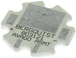
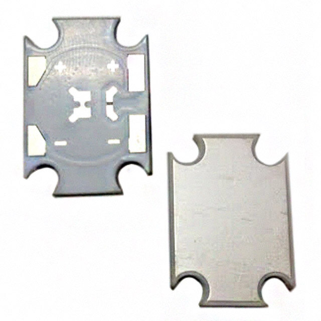
| 描述 | BRD STAR LED IMS AVAGO MOONSTONE热基质 - MCPCB 1-UP INDV STAR AVAGO MOONSTONE |
| 产品分类 | |
| 品牌 | BergquistBergquist Company |
| 产品手册 | |
| 产品图片 |
|
| rohs | 符合RoHS无铅 / 符合限制有害物质指令(RoHS)规范要求 |
| 产品系列 | LED照明机械器件,热基质 - MCPCB,Bergquist Company 803121Thermal Clad® IMS® |
| mouser_ship_limit | 该产品可能需要其他文件才能进口到中国。 |
| 数据手册 | |
| 产品型号 | 803121803121 |
| 产品培训模块 | http://www.digikey.cn/PTM/IndividualPTM.page?site=cn&lang=zhs&ptm=17550 |
| 产品目录绘图 |
|
| 产品目录页面 | |
| 产品种类 | 热基质 - MCPCB |
| 其它名称 | BER265 |
| 包装 | 每包 1 个 |
| 商标 | Bergquist Company |
| 商标名 | Thermal Cladr |
| 导热性 | 1.3 W/m-K |
| 工厂包装数量 | 500 |
| 形状 | 星形 |
| 标准包装 | 500 |
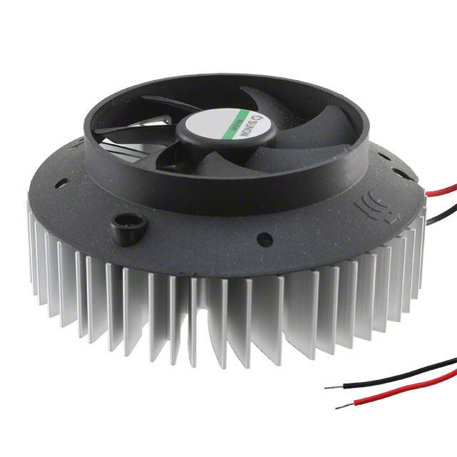
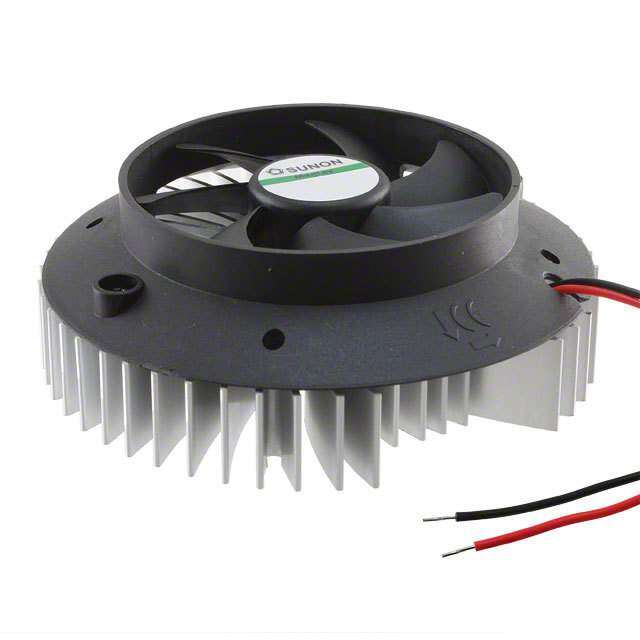
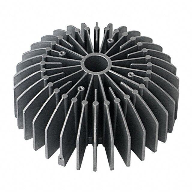
| 相关产品 | /product-detail/zh/ASMT-MYE2-NKM00/ASMT-MYE2-NKM00-ND/2347329/product-detail/zh/ASMT-MYE0-NKM00/ASMT-MYE0-NKM00-ND/2347328/product-detail/zh/ASMT-MYB9-NKM00/ASMT-MYB9-NKM00-ND/2347327/product-detail/zh/ASMT-MYB6-NKM00/ASMT-MYB6-NKM00-ND/2347326/product-detail/zh/ASMT-MYB4-NKL00/ASMT-MYB4-NKL00-ND/2347325/product-detail/zh/ASMT-MY22-NLMZ0/ASMT-MY22-NLMZ0-ND/2347324/product-detail/zh/ASMT-MY22-NLMW0/ASMT-MY22-NLMW0-ND/2347323/product-detail/zh/ASMT-MY22-NLMU0/ASMT-MY22-NLMU0-ND/2347322/product-detail/zh/ASMT-MY22-NLM00/ASMT-MY22-NLM00-ND/2347321/product-detail/zh/ASMT-MY20-NLM00/ASMT-MY20-NLM00-ND/2347320/product-detail/zh/ASMT-MY09-NKM00/ASMT-MY09-NKM00-ND/2347319/product-detail/zh/ASMT-MY06-NKM00/ASMT-MY06-NKM00-ND/2347318/product-detail/zh/ASMT-MY05-NKM00/ASMT-MY05-NKM00-ND/2347317/product-detail/zh/ASMT-MY04-NKL00/ASMT-MY04-NKL00-ND/2347316/product-detail/zh/ASMT-MWE2-NLM00/ASMT-MWE2-NLM00-ND/2347315/product-detail/zh/ASMT-MWE0-NLM00/ASMT-MWE0-NLM00-ND/2347314/product-detail/zh/ASMT-MWB9-NLM00/ASMT-MWB9-NLM00-ND/2347313/product-detail/zh/ASMT-MWB6-NLM00/ASMT-MWB6-NLM00-ND/2347312/product-detail/zh/ASMT-MWB4-NKM00/ASMT-MWB4-NKM00-ND/2347311/product-detail/zh/ASMT-MW22-NLNZ0/ASMT-MW22-NLNZ0-ND/2347310/product-detail/zh/ASMT-MW22-NLNW0/ASMT-MW22-NLNW0-ND/2347309/product-detail/zh/ASMT-MW22-NLNU0/ASMT-MW22-NLNU0-ND/2347308/product-detail/zh/ASMT-MW22-NLNS0/ASMT-MW22-NLNS0-ND/2347307/product-detail/zh/ASMT-MW22-NLN00/ASMT-MW22-NLN00-ND/2347306/product-detail/zh/ASMT-MW09-NLM00/ASMT-MW09-NLM00-ND/2347305/product-detail/zh/ASMT-MW06-NLMZ1/ASMT-MW06-NLMZ1-ND/2347304/product-detail/zh/ASMT-MW06-NLM00/ASMT-MW06-NLM00-ND/2347303/product-detail/zh/ASMT-MW05-NLMZ0/ASMT-MW05-NLMZ0-ND/2347302/product-detail/zh/ASMT-MW05-NLMW0/ASMT-MW05-NLMW0-ND/2347301/product-detail/zh/ASMT-MW05-NLMS0/ASMT-MW05-NLMS0-ND/2347300/product-detail/zh/ASMT-MW05-NLM00/ASMT-MW05-NLM00-ND/2347299/product-detail/zh/ASMT-MW04-NKM00/516-2948-ND/2347298/product-detail/zh/ASMT-MYB9-NKLZ0/ASMT-MYB9-NKLZ0-ND/2211199/product-detail/zh/ASMT-MYB9-NKLW0/ASMT-MYB9-NKLW0-ND/2211198/product-detail/zh/ASMT-MYB9-NKLU0/ASMT-MYB9-NKLU0-ND/2211197/product-detail/zh/ASMT-MYB9-NKL00/ASMT-MYB9-NKL00-ND/2211196/product-detail/zh/ASMT-MYB1-NJK00/ASMT-MYB1-NJK00-ND/2211195/product-detail/zh/ASMT-MY22-NMNZ0/ASMT-MY22-NMNZ0-ND/2211191/product-detail/zh/ASMT-MY22-NMNW0/ASMT-MY22-NMNW0-ND/2211190/product-detail/zh/ASMT-MY22-NMNU0/ASMT-MY22-NMNU0-ND/2211189/product-detail/zh/ASMT-MY09-NLM00/ASMT-MY09-NLM00-ND/2211188/product-detail/zh/ASMT-MY09-NKLZ0/ASMT-MY09-NKLZ0-ND/2211187/product-detail/zh/ASMT-MY09-NKLW0/ASMT-MY09-NKLW0-ND/2211186/product-detail/zh/ASMT-MY09-NKLU0/ASMT-MY09-NKLU0-ND/2211185/product-detail/zh/ASMT-MY09-NKL00/ASMT-MY09-NKL00-ND/2211184/product-detail/zh/ASMT-MY06-NKL00/ASMT-MY06-NKL00-ND/2211183/product-detail/zh/ASMT-MY05-NKL00/ASMT-MY05-NKL00-ND/2211182/product-detail/zh/ASMT-MY04-NJK00/ASMT-MY04-NJK00-ND/2211181/product-detail/zh/ASMT-MY03-NJK00/ASMT-MY03-NJK00-ND/2211180/product-detail/zh/ASMT-MY00-NJKW0/ASMT-MY00-NJKW0-ND/2211179/product-detail/zh/ASMT-MY00-NJK00/ASMT-MY00-NJK00-ND/2211178/product-detail/zh/ASMT-MY00-NHJ00/ASMT-MY00-NHJ00-ND/2211177/product-detail/zh/ASMT-MW22-NNNZ0/ASMT-MW22-NNNZ0-ND/2211156/product-detail/zh/ASMT-MW22-NNNW0/ASMT-MW22-NNNW0-ND/2211155/product-detail/zh/ASMT-MW22-NNNU0/ASMT-MW22-NNNU0-ND/2211154/product-detail/zh/ASMT-MW22-NNNS0/ASMT-MW22-NNNS0-ND/2211153/product-detail/zh/ASMT-MW09-NMM00/ASMT-MW09-NMM00-ND/2211152/product-detail/zh/ASMT-MW09-NLLZ0/ASMT-MW09-NLLZ0-ND/2211151/product-detail/zh/ASMT-MW09-NLLW0/ASMT-MW09-NLLW0-ND/2211150/product-detail/zh/ASMT-MW09-NLLS0/ASMT-MW09-NLLS0-ND/2211149/product-detail/zh/ASMT-MW09-NLL00/ASMT-MW09-NLL00-ND/2211148/product-detail/zh/ASMT-MW09-NKL00/ASMT-MW09-NKL00-ND/2211147/product-detail/zh/ASMT-MW06-NLL00/ASMT-MW06-NLL00-ND/2211146/product-detail/zh/ASMT-MW05-NLL00/ASMT-MW05-NLL00-ND/2211145/product-detail/zh/ASMT-MW04-NJK00/ASMT-MW04-NJK00-ND/2211144/product-detail/zh/ASMT-MW03-NJK00/ASMT-MW03-NJK00-ND/2211143/product-detail/zh/ASMT-MW00-NKKZ0/ASMT-MW00-NKKZ0-ND/2211142/product-detail/zh/ASMT-MW00-NKK00/ASMT-MW00-NKK00-ND/2211141/product-detail/zh/ASMT-MW00-NJKZ0/ASMT-MW00-NJKZ0-ND/2211140/product-detail/zh/ASMT-MW00-NJKW0/ASMT-MW00-NJKW0-ND/2211139/product-detail/zh/ASMT-MW00-NJK01/ASMT-MW00-NJK01-ND/2211138/product-detail/zh/ASMT-MW00-NJJZ0/ASMT-MW00-NJJZ0-ND/2211137/product-detail/zh/ASMT-MW00-NJJW0/ASMT-MW00-NJJW0-ND/2211136/product-detail/zh/ASMT-MW00-NJJS0/ASMT-MW00-NJJS0-ND/2211135/product-detail/zh/ASMT-MW00-NJJC0/ASMT-MW00-NJJC0-ND/2211134/product-detail/zh/ASMT-MW00-NJJ00/ASMT-MW00-NJJ00-ND/2211133/product-detail/zh/ASMT-MW00-NHJ00/ASMT-MW00-NHJ00-ND/2211132/product-detail/zh/ASMT-MW00-NJK00/516-2000-ND/1990398/product-detail/zh/ASMT-MYE2-NMN00/ASMT-MYE2-NMN00-ND/1989257/product-detail/zh/ASMT-MYE0-NMN00/ASMT-MYE0-NMN00-ND/1989256/product-detail/zh/ASMT-MY22-NMN00/516-1975-5-ND/1987563/product-detail/zh/ASMT-MY20-NMN00/516-1974-5-ND/1987562/product-detail/zh/ASMT-MW22-NNN00/516-1973-5-ND/1987561/product-detail/zh/ASMT-MW00-NFI00/516-1712-5-ND/1165537 |
| 类型 | 热包层板 |
| 系列 | Thermal Clad |
| 芯体材料 | Aluminum |
| 设计目的 | Avago Moonstone |
| 配套使用产品/相关产品 | Avago Moonstone™ 发射器 |
| 配置 | Star Board |


- 商务部:美国ITC正式对集成电路等产品启动337调查
- 曝三星4nm工艺存在良率问题 高通将骁龙8 Gen1或转产台积电
- 太阳诱电将投资9.5亿元在常州建新厂生产MLCC 预计2023年完工
- 英特尔发布欧洲新工厂建设计划 深化IDM 2.0 战略
- 台积电先进制程称霸业界 有大客户加持明年业绩稳了
- 达到5530亿美元!SIA预计今年全球半导体销售额将创下新高
- 英特尔拟将自动驾驶子公司Mobileye上市 估值或超500亿美元
- 三星加码芯片和SET,合并消费电子和移动部门,撤换高东真等 CEO
- 三星电子宣布重大人事变动 还合并消费电子和移动部门
- 海关总署:前11个月进口集成电路产品价值2.52万亿元 增长14.8%


PDF Datasheet 数据手册内容提取
Comprehensive Selection Guide THERMAL CLAD
Index THERMAL CLAD THERMAL CLAD Overview ........................................................ 2-3 THERMAL CLAD Applications .......................................................4 THERMAL CLAD Reliability.............................................................5 Dielectrics Selecting Dielectric Materials ....................................................6-7 Dielectric Performance Considerations ...................................... 8 Summary Of Key Dielectric Characteristics ................................ 9 Advanced Circuit Processing .................................................. 10-11 Design Considerations Baseplate Design Considerations. .......................................... 12-13 Selecting A Circuit Layer .........................................................14-15 Electrical Design Considerations ............................................16-17 Assembly Recommendations..................................................18-19 Other BERGQUIST Thermal Products ...................... 20-21 Appendix ........................................................................................ 22 THERMAL CLAD Configurations ....................................... 23 Henkel. Developing solutions for the electronics industry. Proven thermal management solutions and problem-solving partnership. We make it our business to know your business. We understand your problems. We also know that there will always be a better way to help you reach your goals and objectives. To that end, our company continually invests considerable time and money into research and development. Henkel is in the business of solving problems. With our history and experience in the electronics industry, our experts can help find ways to improve your process, control and manage heat, and back it all with exceptional service. Let us show you the value Henkel offers.
GLOBAL SUPPORT with locations in North America, THERMAL INNOVATION Asia and Europe, and sales staff in MANAGEMENT LEADER 30 countries Henkel’s BERGQUIST thermal solutions were often developed for Our solutions to control and specific customer requests manage heat in electronic assemblies and printed circuit boards are used by many of the world’s largest OEMs in a wide range of industries WHY Henkel? Henkel, the leading solution provider for adhesives, sealants and functional coatings worldwide, uses high-quality BERGQUIST thermal management products—like BERGQUIST TCLAD, BERGQUIST SIL-PAD and BERGQUIST LIQUI-BOND—to offer technological solutions for electronics. Beyond that, we work closely with our customers to understand your problems and deliver technologically advanced solutions backed by exceptional service. GLOBAL SUPPLY CHAIN R&D to maintain a reliable supply of Over 10 R&D Centers around the products to our customers world staffed by 3,000 design and application professionals BROAD PRODUCT PORTFOLIO that includes LOCTITE, TECHNOMELT and BERGQUIST products
4 | Comprehensive THERMAL CLAD Selection Guide THERMAL CLAD Overview Key Benefits Of THERMAL CLAD Original Power Board Assembly (Actual) Henkel is the world leader in the development and manufacture of thermally conductive interface materials. THERMAL CLAD Insulated Metal Substrate (IMS®) was developed by Henkel as a thermal management solution for today’s higher watt-density surface mount applications where heat issues are a major concern. THERMAL CLAD substrates minimize thermal impedance and conduct heat more effectively and efficiently than standard printed wiring boards (PWB’s). These substrates are more mechanically robust than thick-film ceramics and direct bond (66) Thru-hole FETs (15) High profile capacitors (9) High profile bus bars copper constructions that are often used in these applications. Total Weight 3.4 lbs (1543.6 g) THERMAL CLAD is a cost-effective solution which can eliminate components, allow for simplified designs, smaller New Power Board Assembly (Actual) devices and an overall less complicated production processes. Additional benefits of THERMAL CLAD include lower operating temperatures, longer component life and increased durability. Henkel's BERGQUIST brand THERMAL CLAD substrates are not limited to use with metal base layers. In one example, power conversion applications can enhance their performance by replacing FR-4 with THERMAL CLAD dielectrics in multi-layer assemblies. In this application, the thickness of the copper circuit layer can be minimized by the high thermal performance of THERMAL CLAD. For additional information on this topic, refer to the “Specialty Applications” section on pages 12-13 (48) FETs (9) Low profile capacitors (5) Low profile bus bars of this guide. Total Weight 0.82 lbs (370.6 g) THERMAL CLAD is a complete thermal management system, unlike traditional technology which uses heat sinks, clips and other mounting hardware. THERMAL CLAD enables low-cost production by eliminating the need for costly manual assembly. THERMAL CLAD Benefits • RoHS and Reach compliant and halogen-free • Lower component operating temperatures • Reduce printed circuit board size Traditionally, cooling an FR-4 board Cooling with THERMAL CLAD can • Increase power density required use of a large heat sink, eliminate the need for heat sinks, • Extend the life of dies interface material and various device clips, cooling fans and other hardware (brackets, screws or clamps); hardware. An automated assembly • Reduce the number of interconnects a configuration requiring labor method will reduce long term costs. • Improve product thermal and mechanical performance intensive manual assembly. • Combine power and control • Improve product durability • Enable better use of surface mount technology • Reduce heat sinks and other mounting hardware, including thermal interface material • Replace fragile ceramic substrates with greater mechanical durability • Henkel is your one-stop source from raw materials to finished circuit boards Conventional methods measured THERMAL CLAD measured junction junction temperature 5W=Tj 43ºC temperature 5W=Tj 35ºC
Comprehensive THERMAL CLAD Selection Guide | 5 Improve Durability and Performance Reduce Board Size and Replace Hardware THERMAL CLAD improves durability because designs can be THERMAL CLAD greatly reduces board space while replacing kept simple while components are kept cool. The low thermal other components including heat sinks. It offers the opportunity impedance of the THERMAL CLAD dielectric outperforms other to eliminate mica and grease or rubber insulators under power insulators for power components, allowing for cooler operation. devices by using direct solder mount to THERMAL CLAD. By eliminating this hardware, heat transfer is improved. THERMAL CLAD keeps assemblies cool by eliminating thermal interfaces and using thermally efficient solder joints. Voltage Interconnects can be eliminated by using etched traces on the breakdown and thermal performance improve in potted THERMAL CLAD board. In fact, whole sections of PWB’s are assemblies using SMD’s and bare die on THERMAL CLAD. often eliminated. It permits the use of surface mount power and passive devices to reduce real estate. With THERMAL CLAD, THERMAL CLAD can also reduce production costs by enabling many discrete devices can be replaced at the board level. automated pick-and-place equipment for SMD’s. The Anatomy Of A THERMAL CLAD Board THERMAL CLAD is a dielectric (ceramic-polymer blend) coated metal base with a bonded copper circuit layer. This unique material offers superior heat transfer to help cool components while eliminating the problems associated with fragile ceramics. Different than others, Henkel's BERGQUIST brand doesn’t use fiberglass, allowing for better thermal performance. THERMAL CLAD is a three layer system comprised of the following: • Circuit Layer: This is the printed circuit foil with a thickness range of .5oz. to 10oz. (17-350µm) in standard THERMAL CLAD. • Dielectric Layer: This offers electrical isolation with minimum thermal resistance. Glass carriers degrade thermal performance which is why our dielectrics are glass-free. CML is the one exception because of its prepreg form, a glass carrier is needed for handling purposes. The dielectric layer is the key element of THERMAL CLAD, and bonds the base metal and circuit metal together. The dielectric has UL recognition, simplifying agency acceptance of final assemblies. • Base Layer: This is often aluminum, but other metals such as Henkel's BERGQUIST manufacturing facility located in Prescott, Wisconsin copper may also be used. The most widely used base material features state-of-the-art process capabilities. Process manufacturing uses the thickness is 0.062'' (1.57mm) in aluminum, although many latest in technology including environmental clean room control, surface thicknesses are available. In some applications, the base finishing, coating and lamination. layer of metal may not be needed. See “Advanced Circuit Processing” on page 12. Circuit Layer Dielectric Layer Base Layer
6 | Comprehensive THERMAL CLAD Selection Guide THERMAL CLAD Applications Power Conversion Heat-Rail And Forming Solid State Relays/Switches Due to the size constraints and The use of THERMAL CLAD in heat-rail The implementation of Solid State Relays watt-density requirements in DC-DC applications has increased significantly in many control applications calls for conversion, THERMAL CLAD has become and is currently used in automotive, thermally efficient, and mechanically the favored choice. THERMAL CLAD audio, motor control and power robust substrates. THERMAL CLAD offers is available in a variety of thermal conversion applications. THERMAL CLAD both. The material construction allows performances, is compatible with offers many advantages including surface mounting configurations not reasonably mechanical fasteners and is highly mount assembly, attachment capabilities possible with ceramic substrates. New reliable. It can be used in almost every and excellent thermal performance. The dielectrics meet the high thermal form-factor and fabricated in a wide dielectric can be selectively removed performance expectations and can variety of substrate metals, thicknesses and the metal can be formed with even out-perform existing ceramic and copper foil weights. three-dimensional features making based designs. THERMAL CLAD a versatile substrate. Motor Drives LEDs Compact high-reliability motor drives In Power LED applications, light output Want to maximize built on THERMAL CLAD have set the and long life are directly attributable benchmark for watt-density. Dielectric to how well the LED’s are managed the lifecycle and color choices provide the electrical isolation thermally. THERMAL CLAD is an excellent necessary to meet operating parameters solution for designers. T-Clad is a metal consistency of your LEDs? and safety agency test requirements. based material (often referred to as With the ability to fabricate in a wide a MCPCB), and can be configured for Henkel's Thermal Management for variety of form-factors, implementation special shapes, bends and thicknesses into either compact or integrated motor thus allowing the designer to put LED LED Applications Solutions Guide drives is realized. The availability light engines in virtually any application. of THERMAL CLAD HT makes high Mounting Power LED’s on T-Clad addresses important factors and temperature operation possible. assures the lowest possible operating temperatures and maximum brightness, recommendations for selecting a color and life. thermal management solution ideal for your LED design.
Comprehensive THERMAL CLAD Selection Guide | 7 THERMAL CLAD Reliability THERMAL CLAD Long Term Reliability Extensive qualification testing consists of mechanical property validation, adhesion, temperature cycling, thermal and New materials undergo a rigorous 12 to 18 month qualification electrical stress. To validate long term reliability, electrical program prior to being released to the market. testing is performed at selected intervals to 2,000 hours In state-of-the-art laboratories and test facilities, Henkel where final evaluation is completed. performs extensive testing on all their thermal materials for To ensure consistent product performance with manufactured electrical integrity. Henkel utilizes stringent development materials, we couple the up-front qualification test with procedures. The lab facilities at Henkel are UL certified and regular audits. Audits include physical, electrical and thermal manufacturing facilities are ISO 9001:2008 certified. property tests. Typical Qualification Programs Physical Properties Electrical Properties Other Properties Evaluated Insulation Impedance Permittivity/Dissipation Thermal Shock Peel Adhesion Breakdown Voltage Temp/Hum/Bias Temp/Hum/Bias Sand Bath Ten Cycle Pull Strength Sequential DC and AC 85C/85%RH/100V 85°C/85%RH/100V 300°C/1 minute and Solder Shock Aging Sequential Aging 2000 hours 2000 hours 200°C/72 hour post Thermal Stress Thermal Stress Thermal Bias Aging Thermal Bias Aging Thermal Flammability Flammability 230°C/10 min. 125°C/100V/2000h 125°C/100V/2000h Conductivity 230°C/10 min. Thermal Aging Thermal Aging Thermal Bias Aging Thermal Bias Aging 125°C/2000 hours 125°C/2000 hours 125°C/480V/2000h 125°C/480V/2000h Temp Cycling Temp Cycling 500 cycles/-40°C-150°C 500 cycles/-40°C-150°C Thermal Bias Aging Thermal Bias Aging 350 hours 350 hours 175°C/100V/2000h 175°C/100V/2000h Temp/Hum/Bias Temp/Hum/Bias 85°C/85%RH/100V 85°C/85%RH/100V 2000 hours 2000 hours Chemical Soak Chemical Soak Loncoterge - 15 min. Loncoterge - 15 min. Alcohol - 15 min. Alcohol - 15 min. Dynamic Mechanical Analysis (DMA) – Measures the Chamber Ovens – Over 3000 cubic feet (85 cubic meters) of Thermogravimetric Analyzer (TGA) – Measures the modulus of materials over a range of temperatures. oven capacity is dedicated to long term thermal bias age stability of our dielectrics at high temperatures, testing. The ovens take material to temperatures above Tg. baking the materials at prescribed temperatures and At selected intervals, samples are removed and tested to measuring weight loss. verify material integrity.
8 | Comprehensive THERMAL CLAD Selection Guide Selecting Dielectric Materials Dielectric Layer Thermal Conductivity The technology of THERMAL CLAD resides in the dielectric layer. It Thermal conductivity is relevant to the application’s thermal is the key element for optimizing performance in your application. performance when the thickness of the dielectric material, The dielectric is a proprietary polymer/ceramic blend that gives interfacial resistance and area are taken into consideration. See THERMAL CLAD its excellent electrical isolation properties and “Thermal Impedance” section for more information, as this data low thermal impedance. will be the most relevant to your application. The polymer is chosen for its electrical isolation properties, ability to resist thermal aging and high bond strengths. The Lower Thermal Performance ceramic filler enhances thermal conductivity and maintains high dielectric strength. The result is a layer of isolation which CML - Circuit Material Laminate can maintain these properties even at 0.0015'' (38µm) thickness. HR T30.20 Contact a Henkel Sales Representative for thinner dielectric MP - Multi-Purpose information. We will help you select the best dielectric to suit your needs for watt-density, electrical isolation and operating HT - High Temperature temperature environment. HPL - High Power Lighting Standardized Methods For Higher Thermal Performance Measuring Thermal Conductivity There are several different test methods for determining a Standardized Test Methods (W/m-K) material’s thermal conductivity value. Results can be different depending on the method chosen, so it is important to use PART NUMBER ASTM D54701 ASTM E14612 similar test methods in material comparisons. See chart at right. HPL-03015 3.0 3.3 Standard test methods include ASTM D5470 and ASTM E1461. HT-04503 2.2 2.0 ASTM D5470 is a steady state method and is referred to as the HT-07006 2.2 2.0 guarded hot plate. This method provides an analytically MP-06503 1.3 1.2 derived value and does not use approximations. ASTM E1461 HR T30.20 1.0 1.1 is a transient method referred to as Laser Flash Diffusivity. In E1461, thermal diffusivity is the test output and thermal Method Description conductivity is calculated. 1 - ASTM D5470 Guarded Hot Plate 2 - ASTM E1461 Laser Flash Diffusivity Non-Standard In-House Test Methods The adjacent chart shows how vastly different thermal conductivity values can be achieved by using “in-house” or Non-Standard Thermal Conductivity non-standard test methods. For example, when the same Test Methods and Model (W/m-K) dielectric is chosen we can derive a completely different and much higher thermal conductivity value by testing a stack-up or GUARDED GUARDED LASER laminate with base layer. We can modify the test further by using PART HOT PLATE HOT PLATE FLASH LASER FLASH different materials for the substrate to obtain even higher results. NUMBER MODEL1 LAMINATE2 LAMINATE3 LAMINATE2 LAMINATE3 Although thermal conductivity values are still relative to one HT-04503 9.0 32.2 36.4 67.6 115 another so a comparison can be made, these test methods do not HT-07006 9.0 21.5 23.3 46.0 86.5 give us an accurate depiction of true thermal performance in the application. Included in the chart is a modeled value for thermal MP-06503 4.5 14.0 24.0 34.9 102 conductivity, a respected model for predicting the effective Method Description thermal conductivity of anisotropic particulate composites, but 1 - Bruggeman Model not helpful for determining thermal performance in application. 2 - Tested with 0.062'' (1.57mm) 5052 aluminum substrate and 2 oz. (70µm) copper foil We emphasize using standard test methods such as ASTM D5470 3 - Tested with 0.062'' (1.57mm) 1100 copper substrate and 2 oz. (70µm) foil and ASTM E1461, which are universally accepted and repeatable. Note: The hot disk method is not a method we use for comparison because typically this method measures the conductivity of the dielectric alone, which neglects thermal interfacial resistance between layers and carrier holding the dielectric. These values must be understood in order to calculate the actual thermal impedance or thermal performance data. See section regarding thermal impedance on page 9.
Comprehensive THERMAL CLAD Selection Guide | 9 Electrical Isolation - Power Applications High Power Lighting Applications Dielectrics are available in thicknesses from 0.0015” (38µm) HPL is a dielectric specifically formulated for high power to 0.009'' (229µm), depending on your isolation needs. See lighting LED applications with demanding thermal performance “Electrical Design Considerations” on pages 18-19 to help requirements. This thin dielectric at 0.0015” (38µm) has an determine which thickness is appropriate for your application. ability to withstand high temperatures with a glass transition of 185°C and phenomenal thermal performance of 0.30°C/W. For detailed information, call Henkel Sales or go online. Breakdown Voltage In Oil with 2'' (51mm) Probe ASTM D149 16 TO-220 Thermal Characterization 14 Measured according to RD 2018 at 40 Watts V] AC Breakdown Voltage [k 116802 HMCHMTRP LT30.20 pedance [°C/W] 11..27 MHCHHMTPRPL LT30.20 m 4 mal I 0.7 .002'' .004'' .006'' .008'' .010'' .012'' her (51) (102) (152) (203) (254) (305) T Dielectric Thickness Inches (μm) 0.2 .000'' .002'' .004'' .006'' .008'' .010'' .012'' .014'' (00) (51) (102) (152) (203) (254) (305) (357) Dielectric Thickness Inches (μm) Thermal Impedance Determines Watt Density Thermal impedance is the only measurement that matters in Thermal Characterization of Dielectrics determining the watt density capability of your application Calculated from ASTM D5470 because it measures the temperature drop across the stack-up 0.5 for each watt of heat flow. Lower thermal impedance results in lower junction temperatures. The lower the thermal impedance, Watt] 0.4 the more efficiently heat travels out of the components. n²/ nce [°C. i 0.3 peda 0.2 HT mal Im MCMPL Ther 0.1 HR T30.20 0.0 .003'' .005'' .007'' .009'' .011'' (76) (127) (178) (229) (279) Dielectric Thickness Inches (μm) Sample Thickness TOTAL IMPEDANCE = + Interfacial Resistance Thermal Conductivity Lower Thermal Impedance = Lower Junction Temperatures
10 | Comprehensive THERMAL CLAD Selection Guide Dielectric Performance Considerations Peel Strength Storage Modulus [N/mm]18[lbs/in] Circuit PAeSeTlM A d2h8e6s1i o(Tny poifc aBle Tregsqt uViasltu Me)aterials 20000 Dynamic Mechanical Analysis (DMA) Results 3 16 HT HT 2.5 14 MP 16000 MP 12 CML Mpa] CML Peel Strength1.251 1068 FHRR- 4T30.20 orage Modulus [ 182000000 HR T30.20 St 4 4000 0.5 2 0 0 0 0 50 100 150 200 250 0 50 100 150 200 Temperature [°C] Temperature [°C] This chart graphs the stability of the bond strength between the dielectric and the This chart depicts the storage modulus of the material over a temperature range. circuit layer during temperature rise. Although bond strength goes down at higher All of our dielectrics are robust, but you will want to choose the one that best suits temperatures, it maintains at least 3 lbs/inch (0.53 N/mm) even at 175°C. your operating temperature environment. See “Assembly Recommendations” on pages 18-19 for additional information. Coefficient of Thermal Expansion Operating THERMAL CLAD Materials Above Tg Above the Tg of the material, mechanical and electrical ThermoMechanical Analysis (TMA) Results properties begin to change. Mechanical changes of note are 12000 a reduction of peel strength of the copper foil, an increase in Material CTE below Tg CTE below Tg °C]m/m 10000 CMLHMTTPIL 43320005 1179210500 tbheen eCfTitE ,o af nredl ideevcinrega rseinsigd sutaolr satgree sms oodnu tlhues .d Tiheleercet riisc a i nptoetrefanctieasl, in ge [μ 8000 HT solder joints and other interconnects due to CTE mismatches by han MP choosing a dielectric with Tg below the operating temperature. on C 6000 CFRM-4L The dielectric material above Tg is in its elastomeric state (much nsi HR T30.20 lower storage modulus), allowing some of the stresses to relax. me Di 4000 Changes in electrical properties must also be considered in nal operation above Tg, although they are typically only important o Fracti 2000 at frequencies above 1 MHz. Effects to consider are changes in the permitivity, dielectric loss and breakdown strength of 0 25 75 125 175 the material. Important Note: Many THERMAL CLAD products Temperature [°C] have UL rating up to 45% higher than their glass transition temperature and are used extensively in applications above rated Tg. Thermomechanical Analysis (TMA) measures the dimensional stability of materials during temperature changes, monitoring the Coefficient of Thermal Expansion (CTE). Note: In the application, the CTE of the base material is a dominant contributor to thermal mechanical stress. See pages 14-15 for base layer selection. CTE OF IMS BOARDS - The concerns in exceeding Tg in standard FR-4 materials from a mechanical standpoint should be tempered when using THERMAL CLAD. The ceramic filler in the polymer matrix of THERMAL CLAD dielectrics results in considerably lower Z-axis expansion than in traditional FR-4 materials, while the low thickness of the dielectric means significantly less strain on plated-through- hole (PTH) connections due to expansion.
Comprehensive THERMAL CLAD Selection Guide | 11 Summary Of Key Product Characteristics Performance Characteristics SINGLE LAYER PRODUCT PERFORMANCE DIELECTRIC PERFORMANCE OTHER Thermal Impedance3 Permittivity6 Dielectric Glass Peel Thickness1 Conductivity2 Breakdown5 Part Number Performance2 [°C in2/W] / [Dielectric Conductivity4 Transition7 Strength8 [.000''/μm] [W/m-K] [kVAC] [°C/W] [°C cm2/W] Constant] [W/m-K] [°C] [lbs/in] / [N/mm] HPL-03015 1.5/38 0.30 0.02 / 0.13 7.5 5.0 6 3.0 185 5 / 0.9 HT-04503 3/76 0.45 0.05 / 0.32 4.1 8.5 7 2.2 150 6 / 1.1 HT-07006 6/152 0.70 0.11 / 0.71 4.1 11.0 7 2.2 150 6 / 1.1 MP-06503 3/76 0.65 0.09 / 0.58 2.4 8.5 6 1.3 90 9 / 1.6 MULTI-LAYER HT-09009 9/229 0.90 0.16 / 1.03 4.1 20.0 7 2.2 150 6 / 1.1 HT-07006 6/152 0.70 0.11 / 0.71 4.1 11.0 7 2.2 150 6 / 1.1 CML-11006* 6/152 1.10 0.21 / 1.35 N/A 10.0 7 1.1 90 10 / 1.8 LAMINATE ONLY HR T30.20 3/76 0.9 0.15 / 0.97 1.5 7.5 7 1.0 90 9 / 1.6 *CML is available in prepreg form only Method Description 1 - Optical 2 - MET-5.4-01-40000- 3 - Calculation from ASTM 5470 6 - ASTM D150 Test Thermal Performance 4 - Extended ASTM 5470 7 - MET-5.4-01-7800 of Insulated Metal 5 - ASTM D149, See page 16 8 - ASTM D2861 Substrates (IMS) Note: For applications with an expected operating voltage of 480 Volts AC or above, Henkel recommends a dielectric thickness greater than 0.003'' (76μm). Note: Circuit design is the most important consideration for determining safety agency compliance. Breakdown Voltage does not represent max operating or proof test voltage. For additional information reference page 16. Operating Temperatures Mechanical and Electrical Lifetime Prediction Bare Dielectric Aged in Air in Laboratory Conditions Choose the dielectric that best suits your operating temperature Analyzed by an Extrapolation to UL 746E environment. For high temperature applications, such as 100,000 Assuming 50% Initial Values = Material Lifetime MP, CML automotive, HT offers the right solution. All of our dielectrics urs] HT are UL recognized. ho e [ m eti MATERIAL RTI - ELECTRO / MECHANICAL PER U.L. 746 E CTI+ Lif HPL 140°C / 140°C 0 / 600 10,000 115 125 135 145 155 165 175 HT 140°C / 140°C 0 / 600 Operating Temperature [°C] MP 130°C / 140°C 0 / 500 (425) CML 130°C / 130°C NA / NA Thermal Performance HR T30.20 150°C / 155°C 0 / 600 This drawing represents the MET-5.4-01-40000-Test Thermal +CTI=Comparative Tracking Index - ASTM D3638 / IEC 60112 Performance of Insulated Metal Substrates (IMS) TO-220 thermal MATERIAL U.L. SOLDER LIMIT RATING performance (25°C Cold Plate Testing). HPL* 325°C / 60 seconds 60 lb Force HT* 325°C / 60 seconds Temperature of MP 300°C / 60 seconds Transistor Base TO-220 CML 260°C / 60 seconds (TT ºC) CSoirlcdueirt Layer (IMS) HR T30.20* 325°C / 60 seconds Dielectric (IMS) Temperature of *Covers all soldering options including Eutectic Gold / Tin. IMS Base Metal Base Plate (IMS) (T ºC) B Greased Interface 25°C Water In Water Out Water-cooled Heatsink (º C ) (T - T ) θ = T B W 40W typ
12 | Comprehensive THERMAL CLAD Selection Guide Advanced Circuit Processing Two-Layer Systems Using When designing circuits using Chip-On-Board (COB) technology it is important to use the appropriate surface finish to achieve THERMAL CLAD Circuits excellent die mounting and wire bond connections. The die attachment is accomplished using SnPb, Pb-free solders, Henkel's BERGQUIST brand dielectrics are ideal for applications eutectic gold/tin solder or an electrical/thermal conductive requiring a two-layer solution. Two-layer constructions adhesive, depending on the application requirements to adhere can provide shielding protection and additional electrical the die to the substrate. The wirebonding performed to make interconnects for higher component density. Henkel's BERGQUIST circuit connections is usually either gold or aluminum. ENEPIG brand dielectrics will provide superior thermal performance (Electroless Nickel/Electroless Palladium/Immersion Gold) over traditional FR-4 constructions. In addition, thermal vias or Immersion Silver is recommended for gold wire and ENIG can maximize thermal capabilities for applications utilizing (Electroless Nickel/ Immersion Gold) for aluminum wire power components. When vias can not be used, selecting higher applications. HT dielectrics are UL solder rated at 325°C/60 performance dielectrics can solve thermal issues independently seconds, enabling Eutectic Gold/Tin solders. (see graph, below). Thermal Modeling of Two-Layer Systems TO-220 at 40 Watts with Infinite Heat Sink 225 No Thermal Vias With Thermal Vias 200 175 mperature [°C] 115205 Tinh eTrCmLAaDl v 2ia l’asy uesre d Cinlo asne -LuEpD v aiepwp loicfa dtiiroenc.t Tdhiee aTtHtaEcRhMmAeLn t Hheeanvkye lc hopaps etrh ue pa btoil i5ty o tzo. (la17m5µinma)t e Case Te10705 smdyisasstxeiipmma ittziooe n t.hermal CdLieA oDr smuobdsturalet.e is used to mount the fai ntihsihcekder o dne pthoes iitn otef rHnTa ld liaeyleecr turitci.lizing 50 Heavy Copper 25 FR-4 FR-4 FR-4 CML HT Circuit Layer Applications requiring heavy copper for high current or heat FR-4 CML HT CML HT Bonding Layer spreading are not limited to single-layer needs. The ability to have Two-Layer Dielectric Choices internal layers of heavy copper can provide greater application The graph depicts the modeled thermal result of various two-layer constructions as flexibility. Direct access to the internal copper layer to directly a function of device case temperature. The emphasis is the thermal effect of proper attach or mount components provides unique applications vias utilization. capability. Look for opportunities to reduce the copper thickness. In many applications, Henkel's BERGQUIST brand TCLAD thermal DBC Replacement performance reduces the need for heavy copper. Replace Ceramic Substrates THERMAL CLAD can replace large- area ceramic substrates. It can also be used as a mechanically durable support for ceramic circuits or direct-bond copper subassemblies. The copper circuit layer of Photographic example of UTC versus a standard 0.062'' (1.57mm) aluminum substrate. THERMAL CLAD has more current carrying capability Ultra Thin Circuits than thick-film ceramic technology. Ultra Thin Circuits (UTC) utilize TCLAD dielectrics without THERMAL CLAD has replaced ceramics and DBC in applications due to mechanical the typical thick base layer. These circuits are often used for robustness and its ability to be fabricated in a wide variety of form-factors. component level packaging where the thick aluminum or copper base is not required for mechanical or thermal mass. The circuit Direct Die Application layer is a “stand-alone” ceramic submount replacement where the heat spreading and heat sinking is done in a different location. In Direct die attach and wirebond are increasingly popular methods addition, UTC can often be used for standard component package of component mounting to THERMAL CLAD substrates. A key mounting. In some cases, the thermal performance and heat benefit to this structure is lower thermal resistance as compared dissipation of the UTC is adequate to eliminate the need for heat to conventional surface mount component packages soldered to sinking altogether. The total profile of a UTC can be as thin as an IMS substrate. 0.009'' (0.23mm) and can be built up into multilayer structures. This type of structure is also available with BOND-PLY 450 thermally conductive PSA tape pre-applied to the back. See page 17 for examples of this format.
Comprehensive THERMAL CLAD Selection Guide | 13 Custom Baseplate Applications Copper Foil Copper Foil Dielectric Removal Area Henkel Dielectric (Circuit) Henkel Dielectric Pedestal (Circuit) Baseplate Dielectric Edge Baseplate Selective Dielectric Removal Pedestal Henkel has developed a process for selectively removing Using a copper base and by selectively removing the dielectric dielectric to expose the baseplate. This surface can be a pedestal can be formed moving the baseplate metal up to be surface finished like the other circuit pads. We are not co-planar with adjacent circuits. limited to geometry or size of the dielectric removal area. Selective removal features can be placed very accurately with respect to the circuits. Copper Foil Copper Foil Henkel Dielectric Henkel Dielectric (Circuit) (Circuit) Baseplate Baseplate Blind Plated Via to Baseplate Electrical/Thermal Via Allows for a copper base metal connection to the surface copper Typical “Thru Via” connecting inner to outer layer. Reduces circuit and the inner-layer copper circuit can also be included if thermal impedance by shortening the thermal path while required. Provides a direct thermal path to baseplate. maintaining electrical isolation. Overplate Thermally Conductive Henkel Copper Foil Polymer Fill Dielectric Baseplate Baseplate (Circuit) Henkel Dielectric Filled Via Filled Via This has been filled with an electrical and thermally conductive This has been filled with an electrical and thermally conductive polymer material. It is also overplated to provide a plateable, polymer material. It is also overplated to provide a plateable, solderable and nearly coplanar surface that is void free. solderable and nearly coplanar surface that is void free. For more detail regarding design and tolerance recommendations for active baseplates, please contact your Henkel representative for a White Paper.
14 | Comprehensive THERMAL CLAD Selection Guide Baseplate Design Considerations THERMAL COEFFICIENT OF MODULUS OF DENSITY YIELD STRENGTH METAL / ALLOY CONDUCTIVITY THERMAL EXPANSION RIGIDITY [g/cc] [MPa] [W/m-K] [ppm/K] [GPa] Copper 400 17 8.9 44.1 310 Aluminum 5052 140 25 2.7 25.9 215 Aluminum 6061 170 25 2.7 26 230 Coefficient Of Thermal Expansion And Heat Spreading Base Layer Selection Considerations 25 400 The adjacent graph depicts the CTE of the baseplate m/K] CTE 350 mthaet emreiatla iln. A rletlhaotiuognhs hAilpu mtoi nthuem h aenadt sCporpepaderin agr ec atphaeb miliotsyt o f on [pp20 Thermal Conductivity 300 W/m-K] pcmooimpsmuplaoatsrc ibthea siss eh apa lfvaaetc ebtsoe rue. snTe hudes ieandd T jiHancE eaRpnMpt ltAiacLba lCteiLo rAneDsp ,wr eohsteehrneetr s Cm sTteEat na ldsa ardn d mal Expansi 15 225000 nductivity [ aCnod enfofni-cstiaenndatr dO bfa sTephlaeter mmaatelr iEalxs.pansion fficient of Ther105 11550000 Thermal Co e And Solder Joints Co 0 0 FR4(x,y) Aluminum Copper Stainless Alumina Silicon Solder joint fatigue can be minimized by selecting the correct Steel base layer to match component expansion. The major concern with thermal expansion is the stress the solder joint experiences in power (or thermal) cycling. Stress induced by heating and cooling may cause the joint to fatigue as it absorbs stress. Large devices, extreme temperature differential, badly mismatched materials, or lead-free minimum solder thickness may all place increased cyclic strain on solder joints. Solder joint fatigue is typically first associated with ceramic Extra Long Circuits based components and with device termination. The section Finished circuits up to 26'' (660mm) long on “Assembly Recommendations” (page 20-21) covers these issues in more detail.
Comprehensive THERMAL CLAD Selection Guide | 15 Base Thickness Surface Finish Copper and aluminum THERMAL CLAD is normally purchased in Aluminum and copper base layers come with a uniform one of the standard-gauge thicknesses shown in the table below. commercial quality brushed surface. Aluminum is also Non-standard thicknesses are also available. available anodized or with other conversion coatings. Electrical Connections To Baseplate Standard THERMAL CLAD Panels If a connection to the base plate is desired, copper is the most Available in: compatible base layer to use. When using electrical or thermal • 18'' (457mm) x 24'' (610mm) vias, it is important to match the circuit and base coefficients Usable area: 17'' (432mm) x 23'' (584mm) of thermal CTE expansion as closely as possible. Otherwise, • 18'' (457mm) x 25'' (635mm) excessive stress to the plated-hole will occur during thermal Usable area: 17'' (432mm) x 24'' (610mm) cycles. Other base layer materials can be used for connection, • 20'' (508mm) x 24'' (610mm) but will require different connection schemes. Usable area: 19'' (483mm) x 23'' (584mm) Costs The most cost effective base layers are aluminum and copper because they represent industry standards. Copper is more expensive than aluminum when comparing the like thicknesses, but can be a competitive option if design considerations allow for a thinner copper base. As an example, typically the cost of 0.040'' (1.0mm) copper is equal to the cost of 0.125'' (3.2mm) aluminum. ALUMINUM - THICKNESSES Inches Millimeters 0.020 0.51 0.032 0.81 0.040* 1.02* 0.062* 1.57* 0.080 2.03 0.125 3.18 0.160 4.06 0.190 4.83 COPPER - THICKNESSES Inches Millimeters 0.020 0.51 0.031 0.79 0.040* 1.02* 0.060 1.52 0.080 2.03 0.125 3.18 *Standard thicknesses
16 | Comprehensive THERMAL CLAD Selection Guide Selecting A Circuit Layer Current Carrying Capabilities The circuit layer is the component-mounting layer in is that the circuit trace interconnecting components can carry THERMAL CLAD. Current carrying capability is a key higher currents because of its ability to dissipate heat due to consideration because this layer typically serves as a I2R loss in the copper circuitry. printed circuit, interconnecting the components of the assembly. The advantage of THERMAL CLAD FR4 FR4 Temperature Rise in Circuit 1 oz (35µm) Temperature Rise in Circuit 1 oz (35µm) due to Current Resistive Heating 2 oz (70µm) due to Current Resistive Heating 3 oz (105µm) 6 oz (210µm) 1'' by 0.125'' (25mm by 3.2mm) trace HT 1'' by 0.125'' (25mm by 3.2mm) trace 10 oz (350µm) on 0.003'' (76μm) HT dielectric 1 oz (35µm) on 0.003'' (76μm) HT dielectric or 0.006'' (152μm) FR-4 dielectric 2 oz (70µm) or 0.006'' (152μm) FR-4 dielectric HT 1 oz (35µm) 10 50 3 oz (105µm) 9 6 oz (210µm) °C]Temperature rise [ 4682537 °C]Temperature rise [ 42310000 10 oz (350µm) 1 0 0 0 5 10 15 20 25 0 50 100 150 200 250 Current [Amps] Current [Amps] Relative temperature rise comparison graph depicts the significant difference Temperature rise comparison graph depicts the significant difference between between Henkel Dielectric HT and FR-4. Additional comparison charts regarding Henkel Dielectric HT and FR-4. Additional comparison charts regarding all all Henkel Dielectrics are available. Note: No base metal used in calculation. Henkel Dielectrics are available. Note: No base metal used in calculation. Want a cost effective, optimized circuit design? This THERMAL CLAD White Paper addresses specific design recommendations including mechanical, circuit, soldermask, fabrication and test options to help optimize your design.
Comprehensive THERMAL CLAD Selection Guide | 17 Heat Spreading Capability Dielectric thickness and foil thickness both influence heat The following graphs depict both the thermal impedance value spreading capability in THERMAL CLAD. Heat spreading is one of and case temperature when relating dielectric and foil thickness. the most powerful advantages derived from IMS. By increasing copper conductor thickness, heat spreading increases and brings junction temperature down. In some cases very heavy copper can be utilized along with bare die to eliminate the need for a standard packaged component. 40 Watt TO-220 soldered to 1" by 1" (25mm x 25mm) 40 Watt TO-220 soldered to 1" by 1" (25mm x 25mm) Thermal Clad MP Thermal Clad MP Henkel RD2018 Test Method Henkel RD2018 Test Method 1.1 85 1 oz (35µm) circuit foil 1 oz (35µm) circuit foil 3 oz (105µm) circuit foil 1.0 3 oz (105µm) circuit foil 80 6 oz (210µm) circuit foil 6 oz (210µm) circuit foil W] 10 oz (350µm) circuit foil mpedance [°C/ 000...987 10 oz (350µm) circuit foil perature [°C] 767055 Thermal I 0.6 Case Tem 60 0.5 55 0.4 50 .002" .003" .004" .005" .006" .007" .002" .003" .004" .005" .006" .007" (51) (76) (102) (127) (152) (178) (51) (76) (102) (127) (152) (178) Dielectric Thickness Inches (µm) Dielectric Thickness Inches (µm ) Standard Circuit Layer Thickness WEIGHT REFERENCE THICKNESS MATERIAL (oz/ft2) inches μm 0.5 0.0007 18 1 0.0014 35 Ultra Thin Circuits utilizing 2 0.0028 70 BOND-PLY 450 PA. See pages 12 and 20 for 3 0.0042 105 Copper additional information. 4 0.0056 140 (Zinc Treatment) 5 0.0070 175 6 0.0084 210 8 0.0112 280 10 0.0140 350 NOTE: Copper foil is NOT measured for thickness as a control method. Instead, it is certified to an area weight requirement per IPC-4562. The nominal thickness given on 1 oz. copper is 0.0014'' (35 µm). CAUTION! Values in IPC-4562 (Table 1.1) are not representative of mechanical thickness.
18 | Comprehensive THERMAL CLAD Selection Guide Electrical Design Considerations Proof Test The use of a DC “Proof Test” is recommended, from an operator safety standpoint. The voltage levels typically used are 1500 The purpose of “Proof Testing” THERMAL CLAD substrates is to to 2250 VDC. Due to the capacitive nature of the circuit board verify that no defects reside in the dielectric material. Because construction, it is necessary to control the ramp up of the testing requires that voltages be above the onset of partial voltage to avoid nuisance tripping of the failure detect circuits discharge, we recommend the number of “Proof Tests” be kept in the tester and to maintain effective control of the test. This is at a minimum. to avoid premature surface arcing or voltage overshoot. There is The term “Partial Discharge” includes a broad spectrum of life safety consideration when DC testing, in that the operator must reducing (i.e. material damaging) phenomena such as: verify the board tested is fully discharged, prior to removing from the test fixture. A more detailed discussion of “Proof Test” 1. Corona discharge is available upon request. 2. Treeing and surface tracking contamination Breakdown Voltage 3. Surface discharges at interfaces, particularly during fault induced voltage reversal The ASTM D149 definition of dielectric breakdown voltage is: 4. Internal discharges in voids or cavities within the dielectric the potential difference at which dielectric failure occurs under prescribed conditions in an electrical insulating material located between two electrodes. This is permanent breakdown and is not recoverable. ASTM goes on to state that the results obtained by this test can seldom be used directly to determine the dielectric behavior of a material in an actual application. This is not a test for “fit for use” in the application, as is the “Proof Test”, which is used for detection of fabrication and material defects to the dielectric insulation. Due to circuit board construction and layout, it is always recommended to “Proof Test” at a value which is less than 50% of the specified ASTM D149 dielectric breakdown voltage. This should include provisions for creepage distance to avoid surface arcing to the metal base. “Proof Test” fixture to test multiple number of finished circuit boards at one time. The purpose of the “Proof Test” is to verify that there has been no degradation of the dielectric insulation due to the fabrication process or any material defects. Continued testing at these voltage levels will only take away from the life of the dielectric on the circuit board. It has been repeatedly verified that “Proof Testing” above the inception of partial discharge (700 VAC or 1200 VAC with proper use of soldermask) will detect any and all defects in the dielectric isolation in the THERMAL CLAD circuit board. Any micro-fractures, delaminations or micro-voids in the dielectric will breakdown or respond as a short during the test.
Comprehensive THERMAL CLAD Selection Guide | 19 Leakage Current HiPot Testing Creepage Distance And Discharge Due to the variety of dielectric types, thicknesses and board Creepage distance and discharge has to be taken into account layouts, not all boards test alike. All insulated metal substrates because THERMAL CLAD dielectrics often incorporate a metal closely resemble a parallel plate capacitor during HiPot testing. base layer. Circuit board designers should consider “Proof Capacitance is equal to: Testing” requirements for: conductor-to-conductor and conductor-to-circuit board edge or through holes. The graphs below depict flashover: without soldermask, with soldermask C = € A/d and under oil. where: € = Permittivity (Dielectric Constant) Typical Flashover Voltage in Various Media A = Surface Area 0.003" (76µm) Dielectric, 25mm circular electrodes d = Distance (Dielectric Thickness) 12000 10000 The capacitance value changes with different configurations of Volts] 8000 Under Oil / Potted moarnaeet aebcroitaualrasdl la yfn atdiel ssb ttoehader d fto elras tyd oiaeunltedsc .at Trnihoci tssh tceraern np gbatsehs deaesn,m db oulenta swktrahageteen d cb uworthrhee nret over Voltage [ 46000000 SAoirlder Mask h in a controlled environment, both pass. Therefore, it is very Flas 2000 important to properly design the testing and test parameters with the material characteristics in mind. Test set-up and 0 0 0.2 0.4 0.6 0.8 1 parameters that over-stress or do not consider reactance of the material and its capacitive and resistive components, can lead to Space Width [mm] false failures and/or test damage of the board. Another test characteristic that is generally misunderstood with Typical Flashover Voltage in Various Media insulated metal substrates is the leakage and charge current that 0.006" (152µm) Dielectric, 25mm circular electrodes take place during the test. In most cases, the leakage current 12000 value on insulated metal substrates is much smaller than the measurement capability of a typical HiPot tester. What is most 10000 misunderstood is the charge current that takes place during Under Oil / Potted 8000 tohnec ete tshte. Lbeoaakradg hea csu brreeennt bmroeausguhrte tmo etnhtes fcualln t oesntl yv oblet argeea l(izDeCd ge [Volts] 6000 SAoirlder Mask vvthoaellut abego aean)r dda. n rTadht eies r dehife/odldrte ai,s ta dt bhiroaeatc rtvdloy lt trhaeagltae th edadus rtaionn gt he tfehf eecca ttpeivasect. i ctTaahnpicase cc iuotafr nrecnet hover Volta 4000 higher than another board will have a higher charge current Flas 2000 rate than the one with a lower effective capacitance. This does 0 not reflect the leakage current or the voltage withstand of the 0 0.2 0.4 0.6 0.8 1 dielectric insulation instead, it represents the characteristic Space Width [mm] transient response of the dielectric. Therefore, one is not able to determine comparable leakage current based on the instantaneous charge current. For accurate leakage test data, bring the board up to full DC test voltage and hold.
20 | Comprehensive THERMAL CLAD Selection Guide Assembly Recommendations Solder Assembly Representative SnPb Reflow Temperature Profile Solder joints deserve additional consideration in the design of THERMAL CLAD assemblies. This section covers solder surface SEovalvpeonrtation FMluextainlg MWeetltting STeunrfsaiocen Vfloulxa tciolimzaptoionne notfs corrosive Oxides Wicking finishes, application and thickness, alloy and flux. 220° C 183° C Flux activation: SSTHtuarEnfRadMcaerAd FL ci nCiriLcsAuhiDet sbcioracurdit fbinoiasrhdess. are available for °C]perature [ 150° C (2-2.5°C(g/Esr)qaduiaelnizta)tion: <5°C ls1i0oql-ud1i5ed°ru Cs boeflow • ENIG (Electroless Nickel/Immersion Gold) m Te • ENEPIG (Electroless Nickel/Electroless Palladium/ Immersion Gold) Reflow Cool-down spike • OSP (Organic Solderability Protectant) Ramp-up Stab(6il0iz-a1t2io0n /ss)oak (>90 s) • Immersion Silver or Immersion Tin Time [Sec] • Lead-Free HASL or Standard Tin/Lead HASL • Electrolytic Gold - for edge connectors Representative Pb free Reflow Temperature Profile Application and Thickness - Solder Paste With the majority of applications now requiring lead-free SEovalvpeonrtation FMOlxueixtdaienlsg MWWeiectlkttiinngg STeunrfsaiocen Vfloulxa tciolimzaptoionne notfs corrosive soldering, there are still some specialized applications using the 250° C Ttaoilin gl-onLnmegae-dtne str omalnd rdee rsl ipoaalbdsietliert .yf .Ii nlTle hetei tr hesoeqlrud iceraers mjeo,ei ntnhtt est hsfiihcnokaunl lesdos scld,o ecmor pmjolypin owtn iietshn k te y °C]perature [ 215105°° CC (gErqaduiaelnizta)tion: <5°C lsF1i0olqul-ud1xi5e da°ru cCst i bvoaeftloiown: m the industry standard: IPC-A-610 “Acceptability of Electronic Te 6° C/s max Assemblies”. The section on solder joints for surface mount 3° C/s max assemblies provides the information on acceptance criteria for Reflow Ramp-down solder joints. It also describes defects that will require rework to spike Ramp-up Stabilization/soak (<30 s) meet acceptance levels. (90-120 s) Time [Sec] Note: Additional thickness and/or larger stencil opening may need to be utilized for RoHS compliance applications. Use profile recommended by the component manufacturer. Now Available TCLAD BOND-PLY 450 PA THERMAL CLAD with BOND-PLY 450 PA is a thermally conductive adhesive tape that features a release liner on the back side for easy removal and application to a heat sink. TCLAD PA substrate release liners can withstand high temperatures and will maintain adhesion and release characteristics even after exposure to the extreme heat of solder reflow. For a complete data sheet, contact Henkel Sales. Wire soldering on THERMAL CLAD. Your most popular LED footprints are available through distribution. Contact Henkel Sales for more information.
Comprehensive THERMAL CLAD Selection Guide | 21 Connection Techniques Connection techniques common throughout the industry are being used successfully on THERMAL CLAD IMS substrates. Surface mount connectors are manufactured using plastic molding materials with thermal coefficients of expansion that roughly match the characteristics of the baseplate metal. However, the plastic molding compounds do have a different thermal capacity and thermal conductivity that can cause stress in the assembly as it cools after soldering and during any significant temperature excursion. Process-caused thermal mechanical stress is specific to the solder reflow process used. For this reason, designs that capture the metal pin without rigidity are preferred, particularly if the major dimension of the connector is large. Pin Connectors Pin connectors and pin headers are often used in Custom Connectors THERMAL CLAD assembly when an FR-4 panel is attached In the example above, the application required a large cable to a THERMAL CLAD assembly. The differential coefficient connection to the TCLAD IMS board. Precautions were taken for of expansion between the control panel and the base metal the best electrical connection with minimized mechanical strain will cause stress in the solder joint and dielectric. The most on the etched circuit. This solution addresses both electrical advanced designs incorporate stress relief in the fabrication and mechanical fastening. The small holes allow for complete of the pin. Redundant header pins are often used to achieve void-free soldering. Also, the insulated shoulder washer high current carrying capacity. prevents shorting to the base plate. These types of connectors are usually custom made and are not commercially available. Wire Bonding Direct Die Attach Wire bonding is particularly useful in the design of packages with Chip-On-Board (COB) architecture. This technique uses the surface mount and interconnect capability of THERMAL CLAD in a highly efficient thermal design. See page 12 for additional information. Manufacturers such as AutoSplice and This Tyco ElectronicsTM SMT thru- Zierick have off the shelf pins ideal for board connector provides a way to IMS applications. Custom pins and bring power from the underside of a connectors are also available. THERMAL CLAD IMS board, eliminating issues of dressing wires on the top side of LED boards. Close up view of a direct Power Connections die attachment in a Only a few companies supply spade or threaded fastener power application. connectors for surface mount power connections. In many cases these are lead frame assemblies soldered to the printed circuit pads and bent to accommodate the shell used for encapsulation. Designs incorporating stress relief and a plastic retainer suitable for high amperage are also available. Thru-board connectors will require adherance to fabrication design rules for IMS PWB’s. Edge Connectors When using edge connectors as part of the THERMAL CLAD printed wiring pattern, it is suggested that interfacing conductors be finished with an electrolytic hard gold plating over sulfamate nickel plating. A 45° chamfer is recommended when using an edge connector. Remember to maintain the minimum edge to conductor distance to prevent shorting. Flex attachment on THERMAL CLAD.
22 | Comprehensive THERMAL CLAD Selection Guide Solutions For Surface-Mount Applications HI-FLOW The HI-FLOW family of phase change materials offers an easy-to-apply thermal interface for many surface mount packages. At the phase change temperature, HI-FLOW materials change from a solid and flow with minimal applied pressure. This characteristic optimizes heat transfer by maximizing wet-out of the interface. HI-FLOW is commonly used to replace messy thermal grease. Henkel phase change materials are specially compounded to prevent pump-out of the interface area, which is often associated with thermal grease. Typical applications for Hi-Flow materials include: • DC/DC converters • Power modules HI-FLOW materials are manufactured with or without film or foil carriers. Custom shapes and sizes for non-standard applications are also available. Power Device THERMAL CLAD HI-FLOW Heat Spreader High Power Application HI-FLOW with THERMAL CLAD Heat Spreader Processor HI-FLOW FR-4 Board High Power Application HI-FLOW without THERMAL CLAD SIL-PAD™ SIL-PAD is the benchmark in thermal interface materials. The SIL-PAD family of materials are thermally conductive and electrically insulating. Available in custom shapes, sheets, and rolls, SIL-PAD materials come in a variety of thicknesses and are frequently used in SMT applications such as: • Interface between thermal vias in a PCB, and a heat sink or casting • Heat sink interface to many surface mount packages Power Device SIL-PAD or BOND-PLY FR-4 Heat Spreader Mid Power Application with BOND-PLY or SIL-PAD
Comprehensive THERMAL CLAD Selection Guide | 23 Where Thermal Solutions Come Together BOND-PLY and LIQUI-BOND The BOND-PLY family of materials are thermally conductive and electrically isolating. Bond-Ply is available in a pressure sensitive adhesive or laminating format. BOND-PLY provides for the mechanical decoupling of bonded materials with mismatched thermal coefficients of expansion. LIQUI-BOND is a high thermal performance liquid silicone adhesive that cures to a solid bonding elastomer. Typical applications include: • Bonding bus bars in a variety of electronic modules and sub assemblies • Attaching a metal-based component to a heat sink • Bonding a heat sink to a variety of ASIC, graphic chip, and CPU packages • Bonding flexible circuits to a rigid heat spreader or thermal plane • Assembly tapes for BGA heat spreader • Attaching PCB assemblies to housings GAP PAD™ and Gap Filler The GAP PAD product family offers a line of thermally conductive materials, in pad or liquid dispensable format, which are highly conformable. Varying degrees of thermal conductivity and compression deflection characteristics are available. Typical applications include: • On top of a semiconductor package such as a QFP or BGA. Often times, several packages with varying heights can use a common heat sink when utilizing GAP PAD. • Between a PCB or substrate and a chassis, frame, or other heat spreader • Areas where heat needs to be transferred to any type of heat spreader • For interfacing pressure sensitive devices • Filling various gaps between heat-generating devices and heat sinks or housings GAP PADs are available in thickness of 0.010'' (0.254mm) to 0.250'' (6.35mm), and in custom shapes, with or without adhesive. Gap Fillers are available in cartridge or kit form. Heat Spreader GAP PAD or Gap Filler Power Device FR-4 Board Lower Power Application with GAP PAD The Path You Take Is Yours Henkel's full line of liquid polymers make it easy to customize your material, pattern, volume and speed. Henkel's advanced liquids are specifically designed to support optimized dispensing control with excellent thermal conductivity. Dispensed in a liquid state the material creates virtually zero stress on components. It can be used to interface and conform to the most intricate topographies and multi-level surfaces.
24 | Comprehensive THERMAL CLAD Selection Guide THERMAL CLAD Configurations Custom Circuit Sheet And Roll Format Henkel's BERGQUIST brand THERMAL CLAD substrates are CML (Circuit Material Laminate) is a ceramic filled polymer custom configured to your design parameters at our Prescott, that forms a strong, thermally conductive bond to metal heat Wisconsin facility. Our field application support personnel in spreaders and is an excellent alternative to pre-preg. conjunction with our mechanical and process engineers are • 24'' (610mm) Roll Standard (custom sizes are available) available to assist you in taking your design from paper to • Maximum roll length of 2000' (610m) finished product. Engineering is available for the following construction parameters and options. • Sheets 18'' x 24'' (457mm x 610mm) and 20'' x 24'' (508mm x 610mm) • Artwork layout recommendations UL Certifications Directory • Base metal requirements and mechanical configuration • Dielectric thickness The U.L. website provides the latest information regarding the • Copper weights (18-350µm / .5-10 oz) UL recognition status of BERGQUIST THERMAL CLAD materials and “Prescott Operations” circuit fabrication. • Solder mask layouts • All common circuit finishes Using the address: http://www.ul.com, select Online Certifications Directory. Enter “BERGQUIST” into the “Company • Tooling/singulation options Name” field and press the search button. Click on the link of Panel Form one of the two U.L. File Numbers to view it: QMTS2.E121882 and ZPMV2.E122713. Additional base metal sizes and thickness options are available • In each group there is guide information which will give a Dimensions: further description of the categories listed. • 18'' x 24'' (457mm x 610mm) • In each group the recognized materials or fabricated circuit 18'' x 25'' (457mm x 635mm) board types will be listed. 20'' x 24'' (508mm x 610mm) QMTS2.E121882 • Foil Thickness: 18-350µm (.5-10 oz) Polymeric Materials - Filament-wound tubing, Industrial Base Plate Metals: Laminates, Vulcanized Fiber, and Materials for Use in Fabricating Recognized Printed Wiring Boards - Components. • Aluminum 6061-T6, 5052-H34, standards from 0.020'' to 0.190'' (0.5mm to 4.83mm) ZPMV2.E122713 • Copper 110 Full-Hard, standard from Wiring, Printed - Component 0.020'' to 0.125'' (0.5mm to 3.2mm)
Comprehensive THERMAL CLAD Selection Guide | 25 Appendix Test Methods for Dielectric Breakdown Voltage and Dielectric Strength of Solid Electrical D 149 Insulating Materials at Commercial Power Frequencies Test Methods for AC Loss Characteristics and Permittivity (Dielectric Constant) of D 150 Solid Electrical Insulating Materials D 257 Test Methods for DC Conductance or Impedance of Insulating Materials ASTM D 374 Test Methods for Thickness of Solid Electrical Insulation Test Method for Strength Properties of Adhesives in Shear by Tension Loading of D 3165 Single-Lap-Joint Laminated Assemblies Test Methods for Thermal Transmission Properties of Thin Thermally Conductive D 5470 Solid Electrical Insulating Materials Methods of test for volume resistivity and surface resistivity of solid 60093 electrical insulating materials Methods of test for electric strength of solid insulating materials - 60243-1 Part 1: Tests at power frequencies IEC Recommended methods for the determination of the permittivity and dielectric 60250 dissipation factor of electrical insulating materials at power, audio, and radio frequencies including metre wavelengths 60626-2 Combined flexible materials for electrical insulation- Part 2: Methods of test 2221 Generic Standard on Printed Board Design 6012 Qualifications and Performance Specification of Rigid Printed Boards 600 Acceptance of Printed Boards TM-650 Cleanliness (2.3.35 & 2.3.26) IPC TM-650-2.4.22 Bow and Twist TM-650-2.4.8 Peel SM-840 Soldermask IPC-A610 Acceptability of Electronic Assemblies Surface Mount IPC-7351 Generic requirements for Surface Mount Design and Land Pattern Standards ISO 4587 Adhesives Determination of tensile lap-shear strength of rigid-to-rigid bonded assemblies
26 | Comprehensive THERMAL CLAD Selection Guide Notes
Comprehensive THERMAL CLAD Selection Guide | 27
® AMERICAS ASIA-PACIFIC EUROPE HEADQUARTERS: CHINA BELGIUM UNITED STATES No. 332 Meigui South Road Henkel Electronics Materials (Belgium) Henkel Electronic Materials, LLC WaiGaoQiao Free Trade Zone, Pu Dong N.V. Nijverheidsstraat 7 14000 Jamboree Road Shanghai 200131, P.R. China B-2260 Westerlo Irvine, CA 92606 Tel: +86.21.3898.4800 Belgium USA Fax: +86.21.5048.4169 Tel: +32.1457.5611 Tel: +1.888.943.6535 Fax: +32.1458.5530 Fax: +1.714.368.2265 Henkel Huawei Electronics CO. LTD Songtiao Industrial Park Lianyungang UNITED KINGDOM Henkel Electronic Materials, LLC Jiangsu Province 222006 China Henkel Ltd. 20021 Susana Road Tel: +86.518.8515.5343 Adhesives Limited Technologies House Rancho Dominguez, CA 90221 Fax: +86.518.8515.3801 Wood Lane End USA Hemel Hempstead Tel: +1.310.764.4600 JAPAN Hertfordshire HP2 4RQ Fax: +1.310.605.2274 Henkel Japan Ltd. Tel: +44.1442.278000 27-7, Shin Isogo-cho Fax: +44.1442.278071 Henkel Electronic Materials, LLC Isogo-ku Yokohama, 235-0017 henkel-adhesives.com/electronics 18930 W. 78th Street Japan technomelt-simply3.com Chanhassen, MN 55317 Tel: +81.45.286.0161 USA Email: jp.ae-csdesk@henkel.com Tel: +1.952.835.2322 Tel: +1.800.347.4572 KOREA Across the Board, Fax: +1.952.835.0430 Henkel Technologies (Korea) Ltd. 6th Floor Around the Globe. BRAZIL Dae Ryung Techno Town II Henkel Brazil 33-33 Gasan-dong, Av. Prof. Vernon Krieble, 91 Geumcheon-gu, Seoul 153-771 06690-070 Itapevi, Korea Sao Paulo, Brazil Tel: +82.2.6675.8000 Tel: +55.11.3205.7001 Fax: +82.2.6675.8191 Fax: +55.11.3205.7100 SINGAPORE Henkel Singapore Pte Ltd. 401, Commonwealth Drive #03-01/02 Haw Par Technocentre, Singapore 149598 Tel: +65.6266.0100 Fax: +65.6472.8738 / +65.6266.1161 www.henkel-adhesives.com/thermal All marks used are trademarks and/or registered trademarks of Henkel and its affiliates in the U.S., Germany and elsewhere. © 2017 Henkel Corporation. All rights reserved. 14868/LT-8145 (Rev. 0217)
Mouser Electronics Authorized Distributor Click to View Pricing, Inventory, Delivery & Lifecycle Information: B ergquist Company: 803121 803122 803123 803124 803125 803126 803127 803128 803129 803261 803262 803263 803265 803266 803267 803268 803269 803281 803282 803283 803284 803285 803286 803287 803288 803289 803291 803293 803772 803790 803803 803805 803808 804068 804069 804070 804087 804090 804091 804092 804155 804450 804511 805245