ICGOO在线商城 > 集成电路(IC) > 逻辑器件 - 转换器,电平移位器 > 74LVCH1T45GM,132
 Datasheet下载
- 型号: 74LVCH1T45GM,132
- 制造商: NXP Semiconductors
- 库位|库存: xxxx|xxxx
- 要求:
| 数量阶梯 | 香港交货 | 国内含税 |
| +xxxx | $xxxx | ¥xxxx |
查看当月历史价格
查看今年历史价格
74LVCH1T45GM,132产品简介:
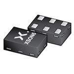
ICGOO电子元器件商城为您提供74LVCH1T45GM,132由NXP Semiconductors设计生产,在icgoo商城现货销售,并且可以通过原厂、代理商等渠道进行代购。 74LVCH1T45GM,132价格参考。NXP Semiconductors74LVCH1T45GM,132封装/规格:逻辑器件 - 转换器,电平移位器, Voltage Level Translator Bidirectional 1 Circuit 1 Channel 420Mbps 6-XSON, SOT886 (1.45x1)。您可以下载74LVCH1T45GM,132参考资料、Datasheet数据手册功能说明书,资料中有74LVCH1T45GM,132 详细功能的应用电路图电压和使用方法及教程。
Nexperia USA Inc.生产的74LVCH1T45GM,132是一款逻辑器件,属于转换器/电平移位器类别。其主要功能是实现不同电压信号之间的电平转换,广泛应用于需要多电压系统通信的场景。以下是该型号的主要应用场景:

1. 嵌入式系统:在嵌入式设备中,常需连接低电压微控制器与高电压外设(如传感器、驱动器等)。74LVCH1T45GM,132可作为双向电平转换器,确保信号在两种电压间可靠传输。

2. 数据总线接口:用于不同电压标准的总线系统之间,例如将3.3V的I/O接口与5V的外围设备连接起来,保证数据完整性并避免损坏敏感元件。

3. 存储器扩展:当扩展外部存储器时,可能遇到主机和存储芯片工作电压不一致的情况。此器件可以解决因电压差异导致的兼容性问题。

4. 通信模块:在无线通信或有线通信模块中,特别是涉及多种供电电压的设计,该芯片能有效进行信号电平适配,支持UART、SPI、I2C等常见通信协议。

5. 电源管理电路:某些情况下,电源管理单元需要与不同的控制逻辑协同工作,这时使用电平转换器能够简化设计并提高效率。

6. 工业自动化:在工业控制系统中,PLC、HMI等人机交互界面往往涉及复杂的多电压环境,这款产品有助于实现稳定的数据交换。

总之,74LVCH1T45GM,132凭借其高效的双向电平转换能力,在现代电子设备中扮演着重要角色,特别是在需要跨电压平台操作的应用场合下表现出色。
| 参数 | 数值 |
| 产品目录 | 集成电路 (IC) |
| 描述 | TXRX XLATING DUAL 3ST XSON6 |
| 产品分类 | 逻辑 - 变换器 |
| 品牌 | NXP Semiconductors |
| 数据手册 | |
| 产品图片 |
|
| 产品型号 | 74LVCH1T45GM,132 |
| PCN封装 | |
| PCN组件/产地 | |
| rohs | 无铅 / 符合限制有害物质指令(RoHS)规范要求 |
| 产品系列 | 74LVCH |
| 产品培训模块 | http://www.digikey.cn/PTM/IndividualPTM.page?site=cn&lang=zhs&ptm=30632 |
| 传播延迟(最大值) | 5.1ns |
| 位数 | 1 |
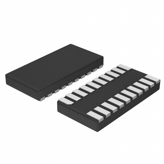
| 供应商器件封装 | 6-XSON,SOT886(1.45x1) |
| 其它名称 | 568-5493-2 |
| 包装 | 带卷 (TR) |
| 安装类型 | 表面贴装 |
| 封装/外壳 | 6-XFDFN |
| 工作温度 | -40°C ~ 125°C |
| 差分-输入:输出 | 无/无 |
| 数据速率 | 420Mbps |
| 标准包装 | 5,000 |
| 电压-电源 | 1.2 V ~ 5.5 V |
| 输入类型 | 逻辑 |
| 输出/通道数 | 1 |
| 输出类型 | 逻辑 |
| 通道数 | 1 |
| 逻辑功能 | 变换器,双向,3 态 |


- 商务部:美国ITC正式对集成电路等产品启动337调查
- 曝三星4nm工艺存在良率问题 高通将骁龙8 Gen1或转产台积电
- 太阳诱电将投资9.5亿元在常州建新厂生产MLCC 预计2023年完工
- 英特尔发布欧洲新工厂建设计划 深化IDM 2.0 战略
- 台积电先进制程称霸业界 有大客户加持明年业绩稳了
- 达到5530亿美元!SIA预计今年全球半导体销售额将创下新高
- 英特尔拟将自动驾驶子公司Mobileye上市 估值或超500亿美元
- 三星加码芯片和SET,合并消费电子和移动部门,撤换高东真等 CEO
- 三星电子宣布重大人事变动 还合并消费电子和移动部门
- 海关总署:前11个月进口集成电路产品价值2.52万亿元 增长14.8%


PDF Datasheet 数据手册内容提取
74LVC1T45; 74LVCH1T45 Dual supply translating transceiver; 3-state Rev. 7 — 19 March 2019 Product data sheet 1. General description The 74LVC1T45; 74LVCH1T45 are single bit, dual supply transceivers with 3-state outputs that enable bidirectional level translation. They feature two 1-bit input-output ports (A and B), a direction control input (DIR) and dual supply pins (V and V ). Both V and V can CC(A) CC(B) CC(A) CC(B) be supplied at any voltage between 1.2 V and 5.5 V making the device suitable for translating between any of the low voltage nodes (1.2 V, 1.5 V, 1.8 V, 2.5 V, 3.3 V and 5.0 V). Pins A and DIR are referenced to V and pin B is referenced to V . A HIGH on DIR allows transmission CC(A) CC(B) from A to B and a LOW on DIR allows transmission from B to A. The devices are fully specified for partial power-down applications using I . The I OFF OFF circuitry disables the output, preventing any damaging backflow current through the device when it is powered down. In suspend mode when either V or V are at GND level, CC(A) CC(B) both A port and B port are in the high-impedance OFF-state. Active bus hold circuitry in the 74LVCH1T45 holds unused or floating data inputs at a valid logic level. 2. Features and benefits • Wide supply voltage range: • V : 1.2 V to 5.5 V CC(A) • V : 1.2 V to 5.5 V CC(B) • High noise immunity • Complies with JEDEC standards: • JESD8-7 (1.2 V to 1.95 V) • JESD8-5 (1.8 V to 2.7 V) • JESD8C (2.7 V to 3.6 V) • JESD36 (4.5 V to 5.5 V) • ESD protection: • HBM JESD22-A114F Class 3A exceeds 4000 V • CDM JESD22-C101E exceeds 1000 V • Maximum data rates: • 420 Mbps (3.3 V to 5.0 V translation) • 210 Mbps (translate to 3.3 V)) • 140 Mbps (translate to 2.5 V) • 75 Mbps (translate to 1.8 V) • 60 Mbps (translate to 1.5 V) • Suspend mode • Latch-up performance exceeds 100 mA per JESD 78 Class II • ±24 mA output drive (V = 3.0 V) CC • Inputs accept voltages up to 5.5 V • Low power consumption: 16 μA maximum I CC • I circuitry provides partial Power-down mode operation OFF • Multiple package options • Specified from -40 °C to +85 °C and -40 °C to +125 °C
Nexperia 74LVC1T45; 74LVCH1T45 Dual supply translating transceiver; 3-state 3. Ordering information Table 1. Ordering information Type number Package Temperature range Name Description Version 74LVC1T45GW -40 °C to +125 °C SC-88 plastic surface-mounted package; 6 leads SOT363 74LVCH1T45GW 74LVC1T45GM -40 °C to +125 °C XSON6 plastic extremely thin small outline package; SOT886 no leads; 6 terminals; body 1 × 1.45 × 0.5 mm 74LVCH1T45GM 74LVC1T45GF -40 °C to +125 °C XSON6 plastic extremely thin small outline package; SOT891 no leads; 6 terminals; body 1 × 1 × 0.5 mm 74LVCH1T45GF 74LVC1T45GN -40 °C to +125 °C XSON6 extremely thin small outline package; no leads; SOT1115 6 terminals; body 0.9 × 1.0 × 0.35 mm 74LVCH1T45GN 74LVC1T45GS -40 °C to +125 °C XSON6 extremely thin small outline package; no leads; SOT1202 6 terminals; body 1.0 × 1.0 × 0.35 mm 74LVCH1T45GS 4. Marking Table 2. Marking Type number Marking code [1] 74LVC1T45GW V5 74LVCH1T45GW X5 74LVC1T45GM V5 74LVCH1T45GM X5 74LVC1T45GF V5 74LVCH1T45GF X5 74LVC1T45GN V5 74LVCH1T45GN X5 74LVC1T45GS V5 74LVCH1T45GS X5 [1] The pin 1 indicator is located on the lower left corner of the device, below the marking code. 5. Functional diagram 5 DIR DIR 3 A A 4 B B VCC(A) VCC(B) VCC(A) VCC(B) 001aag885 001aag886 Fig. 1. Logic symbol Fig. 2. Logic diagram 74LVC_LVCH1T45 All information provided in this document is subject to legal disclaimers. © Nexperia B.V. 2019. All rights reserved Product data sheet Rev. 7 — 19 March 2019 2 / 31
Nexperia 74LVC1T45; 74LVCH1T45 Dual supply translating transceiver; 3-state 6. Pinning information 6.1. Pinning 74LVC1T45 74LVCH1T45 74LVC1T45 74LVC1T45 74LVCH1T45 74LVCH1T45 VCC(A) 1 6 VCC(B) VCC(A) 1 6 VCC(B) VCC(A) 1 6 VCC(B) GND 2 5 DIR GND 2 5 DIR GND 2 5 DIR A 3 4 B A 3 4 B 001aaj993 A 3 4 B 001aaj992 Transparent top view 001aaj991 Transparent top view Fig. 5. Pin configuration SOT891, Fig. 3. Pin configuration SOT363 Fig. 4. Pin configuration SOT886 SOT1115 and SOT1202 (SC-88) (XSON6) (XSON6) 6.2. Pin description Table 3. Pin description Symbol Pin Description V 1 supply voltage port A and DIR CC(A) GND 2 ground (0 V) A 3 data input or output B 4 data input or output DIR 5 direction control V 6 supply voltage port B CC(B) 7. Functional description Table 4. Function table H = HIGH voltage level; L = LOW voltage level; X = don’t care; Z = high-impedance OFF-state. Supply voltage Input Input/output [1] V , V DIR A B CC(A) CC(B) 1.2 V to 5.5 V L A = B input 1.2 V to 5.5 V H input B = A GND [2] X Z Z [1] The input circuit of the data I/O is always active. [2] When either VCC(A) or VCC(B) is at GND level, the device goes into suspend mode. 74LVC_LVCH1T45 All information provided in this document is subject to legal disclaimers. © Nexperia B.V. 2019. All rights reserved Product data sheet Rev. 7 — 19 March 2019 3 / 31
Nexperia 74LVC1T45; 74LVCH1T45 Dual supply translating transceiver; 3-state 8. Limiting values Table 5. Limiting values In accordance with the Absolute Maximum Rating System (IEC 60134). Voltages are referenced to GND (ground = 0 V). Symbol Parameter Conditions Min Max Unit V supply voltage A -0.5 +6.5 V CC(A) V supply voltage B -0.5 +6.5 V CC(B) I input clamping current V < 0 V -50 - mA IK I V input voltage [1] -0.5 +6.5 V I I output clamping current V < 0 V -50 - mA OK O V output voltage Active mode [1][2][3] -0.5 V + 0.5 V O CCO Suspend or 3-state mode [1] -0.5 +6.5 V I output current V = 0 V to V [2] - ±50 mA O O CCO I supply current I or I - 100 mA CC CC(A) CC(B) I ground current -100 - mA GND T storage temperature -65 +150 °C stg P total power dissipation T = -40 °C to +125 °C [4] - 250 mW tot amb [1] The minimum input voltage ratings and output voltage ratings may be exceeded if the input and output current ratings are observed. [2] VCCO is the supply voltage associated with the output port. [3] VCCO + 0.5 V should not exceed 6.5 V. [4] For SC-88 package: above 87.5 °C the value of Ptot derates linearly with 4.0 mW/K. For XSON6 package: above 118 °C the value of Ptot derates linearly with 7.8 mW/K. 9. Recommended operating conditions Table 6. Recommended operating conditions Symbol Parameter Conditions Min Max Unit V supply voltage A 1.2 5.5 V CC(A) V supply voltage B 1.2 5.5 V CC(B) V input voltage 0 5.5 V I V output voltage Active mode [1] 0 V V O CCO Suspend or 3-state mode 0 5.5 V T ambient temperature -40 +125 °C amb Δt/ΔV input transition rise and fall rate V = 1.2 V [2] - 20 ns/V CCI V = 1.4 V to 1.95 V - 20 ns/V CCI V = 2.3 V to 2.7 V - 20 ns/V CCI V = 3 V to 3.6 V - 10 ns/V CCI V = 4.5 V to 5.5 V - 5 ns/V CCI [1] VCCO is the supply voltage associated with the output port. [2] VCCI is the supply voltage associated with the input port. 74LVC_LVCH1T45 All information provided in this document is subject to legal disclaimers. © Nexperia B.V. 2019. All rights reserved Product data sheet Rev. 7 — 19 March 2019 4 / 31
Nexperia 74LVC1T45; 74LVCH1T45 Dual supply translating transceiver; 3-state 10. Static characteristics Table 7. Typical static characteristics at T = 25 °C amb At recommended operating conditions; voltages are referenced to GND (ground = 0 V). [1][2] Symbol Parameter Conditions Min Typ Max Unit V HIGH-level output voltage V = V or V ; I = -3 mA; V = 1.2 V - 1.09 - V OH I IH IL O CCO V LOW-level output voltage V = V or V ; I = 3 mA; V = 1.2 V - 0.07 - V OL I IH IL O CCO I input leakage current DIR input; V = 0 V to 5.5 V; - - ±1 μA I I V = 1.2 V to 5.5 V CCI I bus hold LOW current A or B port; V = 0.42 V; V = 1.2 V - 19 - μA BHL I CCI I bus hold HIGH current A or B port; V = 0.78 V; V = 1.2 V - -19 - μA BHH I CCI I bus hold LOW overdrive A or B port; V = 1.2 V [3] - 19 - μA BHLO CCI current I bus hold HIGH overdrive A or B port; V = 1.2 V [3] - -19 - μA BHHO CCI current I OFF-state output current A or B port; V = 0 V or V ; - - ±1 μA OZ O CCO V = 1.2 V to 5.5 V CCO I power-off leakage current A port; V or V = 0 V to 5.5 V; V = 0 V; - - ±1 μA OFF I O CC(A) V = 1.2 V to 5.5 V CC(B) B port; V or V = 0 V to 5.5 V; V = 0 V; - - ±1 μA I O CC(B) V = 1.2 V to 5.5 V CC(A) C input capacitance DIR input; V = 0 V or 3.3 V; - 2.2 - pF I I V = V = 3.3 V CC(A) CC(B) C input/output capacitance A and B port; suspend mode; - 6.0 - pF I/O V = 3.3 V or 0 V; V = V = 3.3 V O CC(A) CC(B) [1] VCCI is the supply voltage associated with the data input port. [2] VCCO is the supply voltage associated with the output port. [3] To guarantee the node switches, an external driver must source/sink at least IBHLO/IBHHO when the input is in the range VIL to VIH. Table 8. Static characteristics At recommended operating conditions; voltages are referenced to GND (ground = 0 V). [1][2] Symbol Parameter Conditions -40 °C to +85 °C -40 °C to +125 °C Unit Min Max Min Max V HIGH-level data input IH input voltage V = 1.2 V 0.8V - 0.8V - V CCI CCI CCI V = 1.4 V to 1.95 V 0.65V - 0.65V - V CCI CCI CCI V = 2.3 V to 2.7 V 1.7 - 1.7 - V CCI V = 3.0 V to 3.6 V 2.0 - 2.0 - V CCI V = 4.5 V to 5.5 V 0.7V - 0.7V - V CCI CCI CCI DIR input V = 1.2 V 0.8V - 0.8V - V CCI CC(A) CC(A) V = 1.4 V to 1.95 V 0.65V - 0.65V - V CCI CC(A) CC(A) V = 2.3 V to 2.7 V 1.7 - 1.7 - V CCI V = 3.0 V to 3.6 V 2.0 - 2.0 - V CCI V = 4.5 V to 5.5 V 0.7V - 0.7V - V CCI CC(A) CC(A) 74LVC_LVCH1T45 All information provided in this document is subject to legal disclaimers. © Nexperia B.V. 2019. All rights reserved Product data sheet Rev. 7 — 19 March 2019 5 / 31
Nexperia 74LVC1T45; 74LVCH1T45 Dual supply translating transceiver; 3-state Symbol Parameter Conditions -40 °C to +85 °C -40 °C to +125 °C Unit Min Max Min Max V LOW-level data input IL input voltage V = 1.2 V - 0.2V - 0.2V V CCI CCI CCI V = 1.4 V to 1.95 V - 0.35V - 0.35V V CCI CCI CCI V = 2.3 V to 2.7 V - 0.7 - 0.7 V CCI V = 3.0 V to 3.6 V - 0.8 - 0.8 V CCI V = 4.5 V to 5.5 V - 0.3V - 0.3V V CCI CCI CCI DIR input V = 1.2 V - 0.2V - 0.2V V CCI CC(A) CC(A) V = 1.4 V to 1.95 V - 0.35V - 0.35V V CCI CC(A) CC(A) V = 2.3 V to 2.7 V - 0.7 - 0.7 V CCI V = 3.0 V to 3.6 V - 0.8 - 0.8 V CCI V = 4.5 V to 5.5 V - 0.3V - 0.3V V CCI CC(A) CC(A) V HIGH-level V = V OH I IH output voltage I = -100 μA; V = 1.2 V to 4.5 V V - 0.1 - V - 0.1 - V O CCO CCO CCO I = -6 mA; V = 1.4 V 1.0 - 1.0 - V O CCO I = -8 mA; V = 1.65 V 1.2 - 1.2 - V O CCO I = -12 mA; V = 2.3 V 1.9 - 1.9 - V O CCO I = -24 mA; V = 3.0 V 2.4 - 2.4 - V O CCO I = -32 mA; V = 4.5 V 3.8 - 3.8 - V O CCO V LOW-level V = V OL I IL output voltage I = 100 μA; V = 1.2 V to 4.5 V - 0.1 - 0.1 V O CCO I = 6 mA; V = 1.4 V - 0.3 - 0.3 V O CCO I = 8 mA; V = 1.65 V - 0.45 - 0.45 V O CCO I = 12 mA; V = 2.3 V - 0.3 - 0.3 V O CCO I = 24 mA; V = 3.0 V - 0.55 - 0.55 V O CCO I = 32 mA; V = 4.5 V - 0.55 - 0.55 V O CCO I input leakage DIR input; V = 0 V to 5.5 V; - ±2 - ±10 μA I I current V = 1.2 V to 5.5 V CCI I bus hold LOW A or B port BHL current V = 0.49 V; V = 1.4 V 15 - 10 - μA I CCI V = 0.58 V; V = 1.65 V 25 - 20 - μA I CCI V = 0.70 V; V = 2.3 V 45 - 45 - μA I CCI V = 0.80 V; V = 3.0 V 100 - 80 - μA I CCI V = 1.35 V; V = 4.5 V 100 - 100 - μA I CCI I bus hold HIGH A or B port BHH current V = 0.91 V; V = 1.4 V -15 - -10 - μA I CCI V = 1.07 V; V = 1.65 V -25 - -20 - μA I CCI V = 1.60 V; V = 2.3 V -45 - -45 - μA I CCI V = 2.00 V; V = 3.0 V -100 - -80 - μA I CCI V = 3.15 V; V = 4.5 V -100 - -100 - μA I CCI 74LVC_LVCH1T45 All information provided in this document is subject to legal disclaimers. © Nexperia B.V. 2019. All rights reserved Product data sheet Rev. 7 — 19 March 2019 6 / 31
Nexperia 74LVC1T45; 74LVCH1T45 Dual supply translating transceiver; 3-state Symbol Parameter Conditions -40 °C to +85 °C -40 °C to +125 °C Unit Min Max Min Max I bus hold LOW A or B port [3] BHLO overdrive V = 1.6 V 125 - 125 - μA CCI current V = 1.95 V 200 - 200 - μA CCI V = 2.7 V 300 - 300 - μA CCI V = 3.6 V 500 - 500 - μA CCI V = 5.5 V 900 - 900 - μA CCI I bus hold HIGH A or B port [3] BHHO overdrive V = 1.6 V -125 - -125 - μA CCI current V = 1.95 V -200 - -200 - μA CCI V = 2.7 V -300 - -300 - μA CCI V = 3.6 V -500 - -500 - μA CCI V = 5.5 V -900 - -900 - μA CCI I OFF-state A or B port; V = 0 V or V ; - ±2 - ±10 μA OZ O CCO output current V = 1.2 V to 5.5 V CCO I power-off A port; V or V = 0 V to 5.5 V; - ±2 - ±10 μA OFF I O leakage V = 0 V; V = 1.2 V to 5.5 V CC(A) CC(B) current B port; V or V = 0 V to 5.5 V; - ±2 - ±10 μA I O V = 0 V; V = 1.2 V to 5.5 V CC(B) CC(A) I supply current A port; V = 0 V or V ; I = 0 A CC I CCI O V , V = 1.2 V to 5.5 V - 8 - 8 μA CC(A) CC(B) V , V = 1.65 V to 5.5 V - 3 - 3 μA CC(A) CC(B) V = 5.5 V; V = 0 V - 2 - 2 μA CC(A) CC(B) V = 0 V; V = 5.5 V -2 - -2 - μA CC(A) CC(B) B port; V = 0 V or V ; I = 0 A I CCI O V , V = 1.2 V to 5.5 V - 8 - 8 μA CC(A) CC(B) V , V = 1.65 V to 5.5 V - 3 - 3 μA CC(A) CC(B) V = 5.5 V; V = 0 V - 2 - 2 μA CC(B) CC(A) V = 0 V; V = 5.5 V -2 - -2 - μA CC(B) CC(A) A plus B port (I + I ); I = 0 A; CC(A) CC(B) O V = 0 V or V I CCI V , V = 1.2 V to 5.5 V - 16 - 16 μA CC(A) CC(B) V , V = 1.65 V to 5.5 V - 4 - 4 μA CC(A) CC(B) ΔI additional V , V = 3.0 V to 5.5 V CC CC(A) CC(B) supply current A port; A port at V - 0.6 V; [4] - 50 - 75 μA CC(A) DIR at V ; B port = open CC(A) DIR input; DIR at V - 0.6 V; - 50 - 75 μA CC(A) A port at V or GND; CC(A) B port = open B port; B port at V - 0.6 V; [4] - 50 - 75 μA CC(B) DIR at GND; A port = open [1] VCCI is the supply voltage associated with the data input port. [2] VCCO is the supply voltage associated with the output port. [3] To guarantee the node switches, an external driver must source/sink at least IBHLO/IBHHO when the input is in the range VIL to VIH. [4] For non bus hold parts only (74LVC1T45). 74LVC_LVCH1T45 All information provided in this document is subject to legal disclaimers. © Nexperia B.V. 2019. All rights reserved Product data sheet Rev. 7 — 19 March 2019 7 / 31
Nexperia 74LVC1T45; 74LVCH1T45 Dual supply translating transceiver; 3-state 11. Dynamic characteristics Table 9. Typical dynamic characteristics at V = 1.2 V and T = 25 °C CC(A) amb Voltages are referenced to GND (ground = 0 V); for test circuit see Fig. 8; for waveforms see Fig. 6 and Fig. 7 Symbol Parameter Conditions V Unit CC(B) 1.2 V 1.5 V 1.8 V 2.5 V 3.3 V 5.0 V t LOW to HIGH A to B 10.6 8.1 7.0 5.8 5.3 5.1 ns PLH propagation delay B to A 10.6 9.5 9.0 8.5 8.3 8.2 ns t HIGH to LOW A to B 10.1 7.1 6.0 5.3 5.2 5.4 ns PHL propagation delay B to A 10.1 8.6 8.1 7.8 7.6 7.6 ns t HIGH to OFF-state DIR to A 9.4 9.4 9.4 9.4 9.4 9.4 ns PHZ propagation delay DIR to B 12.0 9.4 9.0 7.8 8.4 7.9 ns t LOW to OFF-state DIR to A 7.1 7.1 7.1 7.1 7.1 7.1 ns PLZ propagation delay DIR to B 9.5 7.8 7.7 6.9 7.6 7.0 ns t OFF-state to HIGH DIR to A [1] 20.1 17.3 16.7 15.4 15.9 15.2 ns PZH propagation delay DIR to B [1] 17.7 15.2 14.1 12.9 12.4 12.2 ns t OFF-state to LOW DIR to A [1] 22.1 18.0 17.1 15.6 16.0 15.5 ns PZL propagation delay DIR to B [1] 19.5 16.5 15.4 14.7 14.6 14.8 ns [1] tPZH and tPZL are calculated values using the formula shown in Section 13.4 Table 10. Typical dynamic characteristics at V = 1.2 V and T = 25 °C CC(B) amb Voltages are referenced to GND (ground = 0 V); for test circuit see Fig. 8; for waveforms see Fig. 6 and Fig. 7. Symbol Parameter Conditions V Unit CC(A) 1.2 V 1.5 V 1.8 V 2.5 V 3.3 V 5.0 V t LOW to HIGH A to B 10.6 9.5 9.0 8.5 8.3 8.2 ns PLH propagation delay B to A 10.6 8.1 7.0 5.8 5.3 5.1 ns t HIGH to LOW A to B 10.1 8.6 8.1 7.8 7.6 7.6 ns PHL propagation delay B to A 10.1 7.1 6.0 5.3 5.2 5.4 ns t HIGH to OFF-state DIR to A 9.4 6.5 5.7 4.1 4.1 3.0 ns PHZ propagation delay DIR to B 12.0 6.1 5.4 4.6 4.3 4.0 ns t LOW to OFF-state DIR to A 7.1 4.9 4.5 3.2 3.4 2.5 ns PLZ propagation delay DIR to B 9.5 7.3 6.6 5.9 5.7 5.6 ns t OFF-state to HIGH DIR to A [1] 20.1 15.4 13.6 11.7 11.0 10.7 ns PZH propagation delay DIR to B [1] 17.7 14.4 13.5 11.7 11.7 10.7 ns t OFF-state to LOW DIR to A [1] 22.1 13.2 11.4 9.9 9.5 9.4 ns PZL propagation delay DIR to B [1] 19.5 15.1 13.8 11.9 11.7 10.6 ns [1] tPZH and tPZL are calculated values using the formula shown in Section 13.4 74LVC_LVCH1T45 All information provided in this document is subject to legal disclaimers. © Nexperia B.V. 2019. All rights reserved Product data sheet Rev. 7 — 19 March 2019 8 / 31
Nexperia 74LVC1T45; 74LVCH1T45 Dual supply translating transceiver; 3-state Table 11. Typical power dissipation capacitance at V = V and T = 25 °C CC(A) CC(B) amb Voltages are referenced to GND (ground = 0 V). [1] [2] Symbol Parameter Conditions V and V Unit CC(A) CC(B) 1.8 V 2.5 V 3.3 V 5.5 V C power dissipation A port: (direction A to B); 2 3 3 4 pF PD capacitance B port: (direction B to A) A port: (direction B to A); 15 16 16 18 pF B port: (direction A to B) [1] CPD is used to determine the dynamic power dissipation (PD in μW). PD = CPD × VCC2 × fi × N + Σ(CL × VCC2 × fo) where: fi = input frequency in MHz; fo = output frequency in MHz; CL = load capacitance in pF; VCC = supply voltage in V; N = number of inputs switching; Σ(CL × VCC2 × fo) = sum of the outputs. [2] fi = 10 MHz; VI = GND to VCC; tr = tf = 1 ns; CL = 0 pF; RL = ∞ Ω. Table 12. Dynamic characteristics for temperature range -40 °C to +85 °C Voltages are referenced to GND (ground = 0 V); for test circuit see Fig. 8; for wave forms see Fig. 6 and Fig. 7 Symbol Parameter Conditions V Unit CC(B) 1.5 V 1.8 V 2.5 V 3.3 V 5.0 V ± 0.1 V ± 0.15 V ± 0.2 V ± 0.3 V ± 0.5 V Min Max Min Max Min Max Min Max Min Max V = 1.4 V to 1.6 V CC(A) t LOW to HIGH A to B 2.8 21.3 2.4 17.6 2.0 13.5 1.7 11.8 1.6 10.5 ns PLH propagation delay B to A 2.8 21.3 2.6 19.1 2.3 14.9 2.3 12.4 2.2 12.0 ns t HIGH to LOW A to B 2.6 19.3 2.2 15.3 1.8 11.8 1.7 10.9 1.7 10.8 ns PHL propagation delay B to A 2.6 19.3 2.4 17.3 2.3 13.2 2.2 11.3 2.3 11.0 ns t HIGH to OFF-state DIR to A 3.0 18.7 3.0 18.7 3.0 18.7 3.0 18.7 3.0 18.7 ns PHZ propagation delay DIR to B 3.5 24.8 3.5 23.6 3.0 11.0 3.3 11.3 2.8 10.3 ns t LOW to OFF-state DIR to A 2.4 11.4 2.4 11.4 2.4 11.4 2.4 11.4 2.4 11.4 ns PLZ propagation delay DIR to B 2.8 18.3 3.0 17.2 2.5 9.4 3.0 10.1 2.5 9.4 ns t OFF-state to HIGH DIR to A [1] - 39.6 - 36.3 - 24.3 - 22.5 - 21.4 ns PZH propagation delay DIR to B [1] - 32.7 - 29.0 - 24.9 - 23.2 - 21.9 ns t OFF-state to LOW DIR to A [1] - 44.1 - 40.9 - 24.2 - 22.6 - 21.3 ns PZL propagation delay DIR to B [1] - 38.0 - 34.0 - 30.5 - 29.6 - 29.5 ns 74LVC_LVCH1T45 All information provided in this document is subject to legal disclaimers. © Nexperia B.V. 2019. All rights reserved Product data sheet Rev. 7 — 19 March 2019 9 / 31
Nexperia 74LVC1T45; 74LVCH1T45 Dual supply translating transceiver; 3-state Symbol Parameter Conditions V Unit CC(B) 1.5 V 1.8 V 2.5 V 3.3 V 5.0 V ± 0.1 V ± 0.15 V ± 0.2 V ± 0.3 V ± 0.5 V Min Max Min Max Min Max Min Max Min Max V = 1.65 V to 1.95 V CC(A) t LOW to HIGH A to B 2.6 19.1 2.2 17.7 2.2 9.3 1.7 7.2 1.4 6.8 ns PLH propagation delay B to A 2.4 17.6 2.2 17.7 2.3 16.0 2.1 15.5 1.9 15.1 ns t HIGH to LOW A to B 2.4 17.3 2.0 14.3 1.6 8.5 1.8 7.1 1.7 7.0 ns PHL propagation delay B to A 2.2 15.3 2.0 14.3 2.1 12.9 2.0 12.6 1.8 12.2 ns t HIGH to OFF-state DIR to A 2.9 17.1 2.9 17.1 2.9 17.1 2.9 17.1 2.9 17.1 ns PHZ propagation delay DIR to B 3.2 24.1 3.2 21.9 2.7 11.5 3.0 10.3 2.5 8.2 ns t LOW to OFF-state DIR to A 2.4 10.5 2.4 10.5 2.4 10.5 2.4 10.5 2.4 10.5 ns PLZ propagation delay DIR to B 2.5 17.6 2.6 16.0 2.2 9.2 2.7 8.4 2.4 6.4 ns t OFF-state to HIGH DIR to A [1] - 35.2 - 33.7 - 25.2 - 23.9 - 21.8 ns PZH propagation delay DIR to B [1] - 29.6 - 28.2 - 19.8 - 17.7 - 17.3 ns t OFF-state to LOW DIR to A [1] - 39.4 - 36.2 - 24.4 - 22.9 - 20.4 ns PZL propagation delay DIR to B [1] - 34.4 - 31.4 - 25.6 - 24.2 - 24.1 ns V = 2.3 V to 2.7 V CC(A) t LOW to HIGH A to B 2.3 17.9 2.3 16.0 1.5 8.5 1.3 6.2 1.1 4.8 ns PLH propagation delay B to A 2.0 13.5 2.2 9.3 1.5 8.5 1.4 8.0 1.0 7.5 ns t HIGH to LOW A to B 2.3 15.8 2.1 12.9 1.4 7.5 1.3 5.4 0.9 4.6 ns PHL propagation delay B to A 1.8 11.8 1.9 8.5 1.4 7.5 1.3 7.0 0.9 6.2 ns t HIGH to OFF-state DIR to A 2.1 8.1 2.1 8.1 2.1 8.1 2.1 8.1 2.1 8.1 ns PHZ propagation delay DIR to B 3.0 22.5 3.0 21.4 2.5 11.0 2.8 9.3 2.3 6.9 ns t LOW to OFF-state DIR to A 1.7 5.8 1.7 5.8 1.7 5.8 1.7 5.8 1.7 5.8 ns PLZ propagation delay DIR to B 2.3 14.6 2.5 13.2 2.0 9.0 2.5 8.4 1.8 5.3 ns t OFF-state to HIGH DIR to A [1] - 28.1 - 22.5 - 17.5 - 16.4 - 12.8 ns PZH propagation delay DIR to B [1] - 23.7 - 21.8 - 14.3 - 12.0 - 10.6 ns t OFF-state to LOW DIR to A [1] - 34.3 - 29.9 - 18.5 - 16.3 - 13.1 ns PZL propagation delay DIR to B [1] - 23.9 - 21.0 - 15.6 - 13.5 - 12.7 ns V = 3.0 V to 3.6 V CC(A) t LOW to HIGH A to B 2.3 17.1 2.1 15.5 1.4 8.0 0.8 5.6 0.7 4.4 ns PLH propagation delay B to A 1.7 11.8 1.7 7.2 1.3 6.2 0.7 5.6 0.6 5.4 ns t HIGH to LOW A to B 2.2 15.6 2.0 12.6 1.3 7.0 0.8 5.0 0.7 4.0 ns PHL propagation delay B to A 1.7 10.9 1.8 7.1 1.3 5.4 0.8 5.0 0.7 4.5 ns t HIGH to OFF-state DIR to A 2.3 7.3 2.3 7.3 2.3 7.3 2.3 7.3 2.7 7.3 ns PHZ propagation delay DIR to B 2.9 18.0 2.9 16.5 2.3 10.1 2.7 8.6 2.2 6.3 ns t LOW to OFF-state DIR to A 2.0 5.6 2.0 5.6 2.0 5.6 2.0 5.6 2.0 5.6 ns PLZ propagation delay DIR to B 2.3 13.6 2.4 12.5 1.9 7.8 2.3 7.1 1.7 4.9 ns t OFF-state to HIGH DIR to A [1] - 25.4 - 19.7 - 14.0 - 12.7 - 10.3 ns PZH propagation delay DIR to B [1] - 22.7 - 21.1 - 13.6 - 11.2 - 10.0 ns t OFF-state to LOW DIR to A [1] - 28.9 - 23.6 - 15.5 - 13.6 - 10.8 ns PZL propagation delay DIR to B [1] - 22.9 - 19.9 - 14.3 - 12.3 - 11.3 ns 74LVC_LVCH1T45 All information provided in this document is subject to legal disclaimers. © Nexperia B.V. 2019. All rights reserved Product data sheet Rev. 7 — 19 March 2019 10 / 31
Nexperia 74LVC1T45; 74LVCH1T45 Dual supply translating transceiver; 3-state Symbol Parameter Conditions V Unit CC(B) 1.5 V 1.8 V 2.5 V 3.3 V 5.0 V ± 0.1 V ± 0.15 V ± 0.2 V ± 0.3 V ± 0.5 V Min Max Min Max Min Max Min Max Min Max V = 4.5 V to 5.5 V CC(A) t LOW to HIGH A to B 2.2 16.6 1.9 15.1 1.0 7.5 0.7 5.4 0.5 3.9 ns PLH propagation delay B to A 1.6 10.5 1.4 6.8 1.0 4.8 0.7 4.4 0.5 3.9 ns t HIGH to LOW A to B 2.3 15.3 1.8 12.2 1.0 6.2 0.7 4.5 0.5 3.5 ns PHL propagation delay B to A 1.7 10.8 1.7 7.0 0.9 4.6 0.7 4.0 0.5 3.5 ns t HIGH to OFF-state DIR to A 1.7 5.4 1.7 5.4 1.7 5.4 1.7 5.4 1.7 5.4 ns PHZ propagation delay DIR to B 2.9 17.3 2.9 16.1 2.3 9.7 2.7 8.0 2.5 5.7 ns t LOW to OFF-state DIR to A 1.4 3.7 1.4 3.7 1.3 3.7 1.0 3.7 0.9 3.7 ns PLZ propagation delay DIR to B 2.3 13.1 2.4 12.1 1.9 7.4 2.3 7.0 1.8 4.5 ns t OFF-state to HIGH DIR to A [1] - 23.6 - 18.9 - 12.2 - 11.4 - 8.4 ns PZH propagation delay DIR to B [1] - 20.3 - 18.8 - 11.2 - 9.1 - 7.6 ns t OFF-state to LOW DIR to A [1] - 28.1 - 23.1 - 14.3 - 12.0 - 9.2 ns PZL propagation delay DIR to B [1] - 20.7 - 17.6 - 11.6 - 9.9 - 8.9 ns [1] tPZH and tPZL are calculated values using the formula shown in Section 13.4 Table 13. Dynamic characteristics for temperature range -40 °C to +125 °C Voltages are referenced to GND (ground = 0 V); for test circuit see Fig. 8; for wave forms see Fig. 6 and Fig. 7 Symbol Parameter Conditions V Unit CC(B) 1.5 V 1.8 V 2.5 V 3.3 V 5.0 V ± 0.1 V ± 0.15 V ± 0.2 V ± 0.3 V ± 0.5 V Min Max Min Max Min Max Min Max Min Max V = 1.4 V to 1.6 V CC(A) t LOW to HIGH A to B 2.5 23.5 2.1 19.4 1.8 14.9 1.5 13.0 1.4 11.6 ns PLH propagation delay B to A 2.5 23.5 2.3 21.1 2.0 16.4 2.0 13.7 1.9 13.2 ns t HIGH to LOW A to B 2.3 21.3 1.9 16.9 1.6 13.0 1.5 12.0 1.5 11.9 ns PHL propagation delay B to A 2.3 21.3 2.1 19.1 2.0 14.6 1.9 12.5 2.0 12.1 ns t HIGH to OFF-state DIR to A 2.7 20.6 2.7 20.6 2.7 20.6 2.7 20.6 2.7 20.6 ns PHZ propagation delay DIR to B 3.1 27.3 3.1 26.0 2.7 12.1 2.9 12.5 2.5 11.4 ns t LOW to OFF-state DIR to A 2.1 12.6 2.1 12.6 2.1 12.6 2.1 12.6 2.1 12.6 ns PLZ propagation delay DIR to B 2.5 20.2 2.7 19.0 2.2 10.4 2.7 11.2 2.2 10.4 ns t OFF-state to HIGH DIR to A [1] - 43.7 - 40.1 - 26.8 - 24.9 - 23.6 ns PZH propagation delay DIR to B [1] - 36.1 - 32.0 - 27.5 - 25.6 - 24.2 ns t OFF-state to LOW DIR to A [1] - 48.6 - 45.1 - 26.7 - 25.0 - 23.5 ns PZL propagation delay DIR to B [1] - 41.9 - 37.5 - 33.6 - 32.6 - 32.5 ns 74LVC_LVCH1T45 All information provided in this document is subject to legal disclaimers. © Nexperia B.V. 2019. All rights reserved Product data sheet Rev. 7 — 19 March 2019 11 / 31
Nexperia 74LVC1T45; 74LVCH1T45 Dual supply translating transceiver; 3-state Symbol Parameter Conditions V Unit CC(B) 1.5 V 1.8 V 2.5 V 3.3 V 5.0 V ± 0.1 V ± 0.15 V ± 0.2 V ± 0.3 V ± 0.5 V Min Max Min Max Min Max Min Max Min Max V = 1.65 V to 1.95 V CC(A) t LOW to HIGH A to B 2.3 21.1 1.9 19.5 1.9 10.3 1.5 8.0 1.2 7.5 ns PLH propagation delay B to A 2.1 19.4 1.9 19.5 2.0 17.6 1.8 17.1 1.7 16.7 ns t HIGH to LOW A to B 2.1 19.1 1.8 15.8 1.4 9.4 1.6 7.9 1.5 7.7 ns PHL propagation delay B to A 1.9 16.9 1.8 15.8 1.8 14.2 1.8 13.9 1.6 13.5 ns t HIGH to OFF-state DIR to A 2.6 18.9 2.6 18.9 2.6 18.9 2.6 18.9 2.6 18.9 ns PHZ propagation delay DIR to B 2.8 26.6 2.8 24.1 2.4 12.7 2.7 11.4 2.2 9.1 ns t LOW to OFF-state DIR to A 2.1 11.6 2.1 11.6 2.1 11.6 2.1 11.6 2.1 11.6 ns PLZ propagation delay DIR to B 2.2 19.4 2.3 17.6 1.9 10.2 2.4 9.3 2.1 7.4 ns t OFF-state to HIGH DIR to A [1] - 38.8 - 37.1 - 27.8 - 26.4 - 24.1 ns PZH propagation delay DIR to B [1] - 32.7 - 31.1 - 21.9 - 19.6 - 19.1 ns t OFF-state to LOW DIR to A [1] - 43.5 - 39.9 - 26.9 - 25.3 - 22.6 ns PZL propagation delay DIR to B [1] - 38.0 - 34.7 - 28.3 - 26.8 - 26.6 ns V = 2.3 V to 2.7 V CC(A) t LOW to HIGH A to B 2.0 19.7 2.0 17.6 1.3 9.4 1.1 6.9 0.9 5.3 ns PLH propagation delay B to A 1.8 14.9 1.9 10.3 1.3 9.4 1.2 8.8 0.9 8.3 ns t HIGH to LOW A to B 2.0 17.4 1.8 14.2 1.2 8.3 1.1 6.0 0.8 5.1 ns PHL propagation delay B to A 1.6 13.0 1.7 9.4 1.2 8.3 1.1 7.7 0.8 6.9 ns t HIGH to OFF-state DIR to A 1.8 9.0 1.8 9.0 1.8 9.0 1.8 9.0 1.8 9.0 ns PHZ propagation delay DIR to B 2.7 24.8 2.7 23.6 2.2 12.1 2.5 10.3 2.0 7.6 ns t LOW to OFF-state DIR to A 1.5 6.4 1.5 6.4 1.5 6.4 1.5 6.4 1.5 6.4 ns PLZ propagation delay DIR to B 2.0 16.1 2.2 14.6 1.8 9.9 2.2 9.3 1.6 5.9 ns t OFF-state to HIGH DIR to A [1] - 31.0 - 24.9 - 19.3 - 18.1 - 14.2 ns PZH propagation delay DIR to B [1] - 26.1 - 24.0 - 15.8 - 13.3 - 11.7 ns t OFF-state to LOW DIR to A [1] - 37.8 - 33.0 - 20.4 - 18.0 - 14.5 ns PZL propagation delay DIR to B [1] - 26.4 - 23.2 - 17.3 - 15.0 - 14.1 ns V = 3.0 V to 3.6 V CC(A) t LOW to HIGH A to B 2.0 18.9 1.8 17.1 1.2 8.8 0.7 6.2 0.6 4.9 ns PLH propagation delay B to A 1.5 13.0 1.5 8.0 1.1 6.9 0.6 6.2 0.5 6.0 ns t HIGH to LOW A to B 1.9 17.2 1.8 13.9 1.1 7.7 0.7 5.5 0.6 4.4 ns PHL propagation delay B to A 1.5 12.0 1.6 7.9 1.1 6.0 0.7 5.5 0.6 5.0 ns t HIGH to OFF-state DIR to A 2.0 8.1 2.0 8.1 2.0 8.1 2.0 8.1 2.4 8.1 ns PHZ propagation delay DIR to B 2.6 19.8 2.6 18.2 2.0 11.2 2.4 9.5 1.9 7.0 ns t LOW to OFF-state DIR to A 1.8 6.2 1.8 6.2 1.8 6.2 1.8 6.2 1.8 6.2 ns PLZ propagation delay DIR to B 2.0 15.0 2.1 13.8 1.7 8.6 2.0 7.9 1.5 5.4 ns t OFF-state to HIGH DIR to A [1] - 28.0 - 21.8 - 15.5 - 14.1 - 11.4 ns PZH propagation delay DIR to B [1] - 25.1 - 23.3 - 15.0 - 12.4 - 11.1 ns t OFF-state to LOW DIR to A [1] - 31.8 - 26.1 - 17.2 - 15.0 - 12.0 ns PZL propagation delay DIR to B [1] - 25.3 - 22.0 - 15.8 - 13.6 - 12.5 ns 74LVC_LVCH1T45 All information provided in this document is subject to legal disclaimers. © Nexperia B.V. 2019. All rights reserved Product data sheet Rev. 7 — 19 March 2019 12 / 31
Nexperia 74LVC1T45; 74LVCH1T45 Dual supply translating transceiver; 3-state Symbol Parameter Conditions V Unit CC(B) 1.5 V 1.8 V 2.5 V 3.3 V 5.0 V ± 0.1 V ± 0.15 V ± 0.2 V ± 0.3 V ± 0.5 V Min Max Min Max Min Max Min Max Min Max V = 4.5 V to 5.5 V CC(A) t LOW to HIGH A to B 1.9 18.3 1.7 16.7 0.9 8.3 0.6 6.0 0.4 4.3 ns PLH propagation delay B to A 1.4 11.6 1.2 7.5 0.9 5.3 0.6 4.9 0.4 4.3 ns t HIGH to LOW A to B 2.0 16.9 1.6 13.5 0.9 6.9 0.6 5.0 0.4 3.9 ns PHL propagation delay B to A 1.5 11.9 1.5 7.7 0.8 5.1 0.6 4.4 0.4 3.9 ns t HIGH to OFF-state DIR to A 1.5 6.0 1.5 6.0 1.5 6.0 1.5 6.0 1.5 6.0 ns PHZ propagation delay DIR to B 2.6 19.1 2.6 17.8 2.0 10.7 2.4 8.8 2.2 6.3 ns t LOW to OFF-state DIR to A 1.2 4.1 1.2 4.1 1.1 4.1 0.9 4.1 0.8 4.1 ns PLZ propagation delay DIR to B 2.0 14.5 2.1 13.4 1.7 8.2 2.0 7.7 1.6 5.0 ns t OFF-state to HIGH DIR to A [1] - 26.1 - 20.9 - 13.5 - 12.6 - 9.3 ns PZH propagation delay DIR to B [1] - 22.4 - 20.8 - 12.4 - 10.1 - 8.4 ns t OFF-state to LOW DIR to A [1] - 31.0 - 25.5 - 15.8 - 13.2 - 10.2 ns PZL propagation delay DIR to B [1] - 22.9 - 19.5 - 12.9 - 11.0 - 9.9 ns [1] tPZH and tPZL are calculated values using the formula shown in Section 13.4 11.1. Waveforms and test circuit VI A, B input VM GND tPHL tPLH VOH B, A output VM VOL 001aae967 Measurement points are given in Table 14. V and V are typical output voltage levels that occur with the output load. OL OH Fig. 6. The data input (A, B) to output (B, A) propagation delay times 74LVC_LVCH1T45 All information provided in this document is subject to legal disclaimers. © Nexperia B.V. 2019. All rights reserved Product data sheet Rev. 7 — 19 March 2019 13 / 31
Nexperia 74LVC1T45; 74LVCH1T45 Dual supply translating transceiver; 3-state VI DIR input VM GND tPLZ tPZL VCCO output LOW-to-OFF VM OFF-to-LOW VOL VX tPHZ tPZH output VOH VY HIGH-to-OFF VM OFF-to-HIGH GND outputs outputs outputs enabled disabled enabled 001aae968 Measurement points are given in Table 14. V and V are typical output voltage levels that occur with the output load. OL OH Fig. 7. Enable and disable times Table 14. Measurement points Supply voltage Input [1] Output [2] V , V V V V V CC(A) CC(B) M M X Y 1.2 V to 1.6 V 0.5V 0.5V V + 0.1 V V - 0.1 V CCI CCO OL OH 1.65 V to 2.7 V 0.5V 0.5V V + 0.15 V V - 0.15 V CCI CCO OL OH 3.0 V to 5.5 V 0.5V 0.5V V + 0.3 V V - 0.3 V CCI CCO OL OH [1] VCCI is the supply voltage associated with the data input port. [2] VCCO is the supply voltage associated with the output port. 74LVC_LVCH1T45 All information provided in this document is subject to legal disclaimers. © Nexperia B.V. 2019. All rights reserved Product data sheet Rev. 7 — 19 March 2019 14 / 31
Nexperia 74LVC1T45; 74LVCH1T45 Dual supply translating transceiver; 3-state tW VI 90 % negative pulse VM VM 10 % 0 V tf tr tr tf VI 90 % positive pulse VM VM 10 % 0 V tW VEXT VCC RL VI VO G DUT RT CL RL 001aae331 Test data is given in Table 15. R = Load resistance. L C = Load capacitance including jig and probe capacitance. L R = Termination resistance. T V = External voltage for measuring switching times. EXT Fig. 8. Test circuit for measuring switching times Table 15. Test data Supply voltage Input Load V EXT V , V V [1] Δt/ΔV [2] C R t , t t , t t , t [3] CC(A) CC(B) I L L PLH PHL PZH PHZ PZL PLZ 1.2 V to 5.5 V V ≤ 1.0 ns/V 15 pF 2 kΩ open GND 2V CCI CCO [1] VCCI is the supply voltage associated with the data input port. [2] dV/dt ≥ 1.0 V/ns [3] VCCO is the supply voltage associated with the output port. 74LVC_LVCH1T45 All information provided in this document is subject to legal disclaimers. © Nexperia B.V. 2019. All rights reserved Product data sheet Rev. 7 — 19 March 2019 15 / 31
Nexperia 74LVC1T45; 74LVCH1T45 Dual supply translating transceiver; 3-state 12. Typical propagation delay characteristics 001aai907 001aai908 14 14 tPHL tPLH (ns) (ns) 12 12 (1) (1) 10 10 (2) 8 (2) 8 (3) (3) 6 (4) 6 ((45)) (5) (6) (6) 4 4 2 2 0 0 0 5 10 15 20 25 30 35 0 5 10 15 20 25 30 35 CL (pF) CL (pF) a. HIGH to LOW propagation delay (A to B) b. LOW to HIGH propagation delay (A to B) 001aai909 001aai910 14 14 tPHL tPLH (ns) (ns) 12 12 (1) (1) (2) (3) 10 (2) 10 (4) (3) (5) 8 (4) 8 (5) (6) (6) 6 6 4 4 2 2 0 0 0 5 10 15 20 25 30 35 0 5 10 15 20 25 30 35 CL (pF) CL (pF) c. HIGH to LOW propagation delay (B to A) d. LOW to HIGH propagation delay (B to A) (1) V = 1.2 V. CC(B) (2) V = 1.5 V. CC(B) (3) V = 1.8 V. CC(B) (4) V = 2.5 V. CC(B) (5) V = 3.3 V. CC(B) (6) V = 5.0 V. CC(B) Fig. 9. Typical propagation delay vs load capacitance; T = 25 °C; V = 1.2 V amb CC(A) 74LVC_LVCH1T45 All information provided in this document is subject to legal disclaimers. © Nexperia B.V. 2019. All rights reserved Product data sheet Rev. 7 — 19 March 2019 16 / 31
Nexperia 74LVC1T45; 74LVCH1T45 Dual supply translating transceiver; 3-state 001aai911 001aai912 14 14 tPHL tPLH (ns) (ns) 12 12 (1) 10 (1) 10 8 8 (2) (2) (3) 6 (3) 6 (4) (4) (5) 4 4 (6) (5) 2 (6) 2 0 0 0 5 10 15 20 25 30 35 0 5 10 15 20 25 30 35 CL (pF) CL (pF) a. HIGH to LOW propagation delay (A to B) b. LOW to HIGH propagation delay (A to B) 001aai913 001aai914 14 14 tPHL tPLH (ns) (ns) 12 12 10 10 (1) 8 (1) 8 (2) (2) (3) (3) (4) 6 (4) 6 (5) (5) (6) 4 (6) 4 2 2 0 0 0 5 10 15 20 25 30 35 0 5 10 15 20 25 30 35 CL (pF) CL (pF) c. HIGH to LOW propagation delay (B to A) d. LOW to HIGH propagation delay (B to A) (1) V = 1.2 V. CC(B) (2) V = 1.5 V. CC(B) (3) V = 1.8 V. CC(B) (4) V = 2.5 V. CC(B) (5) V = 3.3 V. CC(B) (6) V = 5.0 V. CC(B) Fig. 10. Typical propagation delay vs load capacitance; T = 25 °C; V = 1.5 V amb CC(A) 74LVC_LVCH1T45 All information provided in this document is subject to legal disclaimers. © Nexperia B.V. 2019. All rights reserved Product data sheet Rev. 7 — 19 March 2019 17 / 31
Nexperia 74LVC1T45; 74LVCH1T45 Dual supply translating transceiver; 3-state 001aai915 001aai916 14 14 tPHL tPLH (ns) (ns) 12 12 (1) 10 10 (1) 8 8 (2) (2) 6 6 (3) (3) (4) 4 (4) 4 (5) (5) (6) (6) 2 2 0 0 0 5 10 15 20 25 30 35 0 5 10 15 20 25 30 35 CL (pF) CL (pF) a. HIGH to LOW propagation delay (A to B) b. LOW to HIGH propagation delay (A to B) 001aai917 001aai918 14 14 tPHL tPLH (ns) (ns) 12 12 10 10 8 8 (1) (1) (2) 6 (2) 6 (3) (3) (4) (4) (5) 4 (5) 4 (6) (6) 2 2 0 0 0 5 10 15 20 25 30 35 0 5 10 15 20 25 30 35 CL (pF) CL (pF) c. HIGH to LOW propagation delay (B to A) d. LOW to HIGH propagation delay (B to A) (1) V = 1.2 V. CC(B) (2) V = 1.5 V. CC(B) (3) V = 1.8 V. CC(B) (4) V = 2.5 V. CC(B) (5) V = 3.3 V. CC(B) (6) V = 5.0 V. CC(B) Fig. 11. Typical propagation delay vs load capacitance; T = 25 °C; V = 1.8 V amb CC(A) 74LVC_LVCH1T45 All information provided in this document is subject to legal disclaimers. © Nexperia B.V. 2019. All rights reserved Product data sheet Rev. 7 — 19 March 2019 18 / 31
Nexperia 74LVC1T45; 74LVCH1T45 Dual supply translating transceiver; 3-state 001aai919 001aai920 14 14 tPHL tPLH (ns) (ns) 12 12 10 10 (1) (1) 8 8 (2) 6 (2) 6 (3) (3) 4 (4) 4 (4) (5) (5) (6) (6) 2 2 0 0 0 5 10 15 20 25 30 35 0 5 10 15 20 25 30 35 CL (pF) CL (pF) a. HIGH to LOW propagation delay (A to B) b. LOW to HIGH propagation delay (A to B) 001aai921 001aai922 14 14 tPHL tPLH (ns) (ns) 12 12 10 10 8 8 (1) 6 (1) 6 (2) (2) (3) 4 (3) 4 (4) (4) (5) (5) (6) 2 (6) 2 0 0 0 5 10 15 20 25 30 35 0 5 10 15 20 25 30 35 CL (pF) CL (pF) c. HIGH to LOW propagation delay (B to A) d. LOW to HIGH propagation delay (B to A) (1) V = 1.2 V. CC(B) (2) V = 1.5 V. CC(B) (3) V = 1.8 V. CC(B) (4) V = 2.5 V. CC(B) (5) V = 3.3 V. CC(B) (6) V = 5.0 V. CC(B) Fig. 12. Typical propagation delay vs load capacitance; T = 25 °C; V = 2.5 V amb CC(A) 74LVC_LVCH1T45 All information provided in this document is subject to legal disclaimers. © Nexperia B.V. 2019. All rights reserved Product data sheet Rev. 7 — 19 March 2019 19 / 31
Nexperia 74LVC1T45; 74LVCH1T45 Dual supply translating transceiver; 3-state 001aai923 001aai924 14 14 tPHL tPLH (ns) (ns) 12 12 10 10 (1) (1) 8 8 (2) 6 (2) 6 (3) (3) 4 4 (4) (4) (5) (5) (6) (6) 2 2 0 0 0 5 10 15 20 25 30 35 0 5 10 15 20 25 30 35 CL (pF) CL (pF) a. HIGH to LOW propagation delay (A to B) b. LOW to HIGH propagation delay (A to B) 001aai925 001aai926 14 14 tPHL tPLH (ns) (ns) 12 12 10 10 8 8 6 (1) 6 (1) (2) (2) 4 (3) 4 (3) (4) (4) (5) (5) 2 (6) 2 (6) 0 0 0 5 10 15 20 25 30 35 0 5 10 15 20 25 30 35 CL (pF) CL (pF) c. HIGH to LOW propagation delay (B to A) d. LOW to HIGH propagation delay (B to A) (1) V = 1.2 V. CC(B) (2) V = 1.5 V. CC(B) (3) V = 1.8 V. CC(B) (4) V = 2.5 V. CC(B) (5) V = 3.3 V. CC(B) (6) V = 5.0 V. CC(B) Fig. 13. Typical propagation delay vs load capacitance; T = 25 °C; V = 3.3 V amb CC(A) 74LVC_LVCH1T45 All information provided in this document is subject to legal disclaimers. © Nexperia B.V. 2019. All rights reserved Product data sheet Rev. 7 — 19 March 2019 20 / 31
Nexperia 74LVC1T45; 74LVCH1T45 Dual supply translating transceiver; 3-state 001aai927 001aai928 14 14 tPHL tPLH (ns) (ns) 12 12 10 10 (1) (1) 8 8 (2) 6 (2) 6 (3) (3) 4 4 (4) (4) (5) (5) (6) (6) 2 2 0 0 0 5 10 15 20 25 30 35 0 5 10 15 20 25 30 35 CL (pF) CL (pF) a. HIGH to LOW propagation delay (A to B) b. LOW to HIGH propagation delay (A to B) 001aai929 001aai930 14 14 tPHL tPLH (ns) (ns) 12 12 10 10 8 8 6 (1) 6 (1) 4 (2) 4 (2) (3) (3) (4) (4) 2 (5) 2 (5) (6) (6) 0 0 0 5 10 15 20 25 30 35 0 5 10 15 20 25 30 35 CL (pF) CL (pF) c. HIGH to LOW propagation delay (B to A) d. LOW to HIGH propagation delay (B to A) (1) V = 1.2 V. CC(B) (2) V = 1.5 V. CC(B) (3) V = 1.8 V. CC(B) (4) V = 2.5 V. CC(B) (5) V = 3.3 V. CC(B) (6) V = 5.0 V. CC(B) Fig. 14. Typical propagation delay vs load capacitance; T = 25 °C; V = 5.0 V amb CC(A) 74LVC_LVCH1T45 All information provided in this document is subject to legal disclaimers. © Nexperia B.V. 2019. All rights reserved Product data sheet Rev. 7 — 19 March 2019 21 / 31
Nexperia 74LVC1T45; 74LVCH1T45 Dual supply translating transceiver; 3-state 13. Application information 13.1. Unidirectional logic level-shifting application The circuit given in Fig. 15 is an example of the 74LVC1T45; 74LVCH1T45 being used in a unidirectional logic level-shifting application. 74LVC1T45 74LVCH1T45 VCC1 VCC2 VCC(A) VCC(B) 1 6 GND DIR VCC1 2 5 VCC2 A B 3 4 system-1 system-2 001aaj994 Fig. 15. Unidirectional logic level-shifting application Table 16. Description unidirectional logic level-shifting application Pin Name Function Description 1 V V supply voltage of system-1 (1.2 V to 5.5 V) CC(A) CC1 2 GND GND device GND 3 A OUT output level depends on V voltage CC1 4 B IN input threshold value depends on V voltage CC2 5 DIR DIR the GND (LOW level) determines B port to A port direction 6 V V supply voltage of system-2 (1.2 V to 5.5 V) CC(B) CC2 13.2. Bidirectional logic level-shifting application Fig. 16 shows the 74LVC1T45; 74LVCH1T45 being used in a bidirectional logic level-shifting application. Since the device does not have an output enable pin, the system designer should take precautions to avoid bus contention between system-1 and system-2 when changing directions. 74LVC1T45 74LVCH1T45 VCC1 VCC1 VCC2 VCC2 VCC(A) VCC(B) I/O-1 1 6 I/O-2 PULL-UP/DOWN GND 2 5 DIR PULL-UP/DOWN A B 3 4 DIR CTRL system-1 system-2 001aaj995 Pull-up or pull-down only needed for 74LVC1T45. Fig. 16. Bidirectional logic level-shifting application 74LVC_LVCH1T45 All information provided in this document is subject to legal disclaimers. © Nexperia B.V. 2019. All rights reserved Product data sheet Rev. 7 — 19 March 2019 22 / 31
Nexperia 74LVC1T45; 74LVCH1T45 Dual supply translating transceiver; 3-state Table 17 provides a sequence that illustrates data transmission from system-1 to system-2 and then from system-2 to system-1. Table 17. Description bidirectional logic level-shifting application H = HIGH voltage level; L = LOW voltage level; Z = high-impedance OFF-state. State DIR CTRL I/O-1 I/O-2 Description 1 H output input system-1 data to system-2 2 H Z Z system-2 is getting ready to send data to system-1. I/O-1 and I/O-2 are disabled. The bus-line state depends on bus hold. 3 L Z Z DIR bit is set LOW. I/O-1 and I/O-2 are still disabled. The bus-line state depends on bus hold. 4 L input output system-2 data to system-1 13.3. Power-up considerations The device is designed such that no special power-up sequence is required other than GND being applied first. Table 18. Typical total supply current (I + I ) CC(A) CC(B) V V Unit CC(A) CC(B) 0 V 1.8 V 2.5 V 3.3 V 5.0 V 0 V 0 < 1 < 1 < 1 < 1 μA 1.8 V < 1 < 2 < 2 < 2 2 μA 2.5 V < 1 < 2 < 2 < 2 < 2 μA 3.3 V < 1 < 2 < 2 < 2 < 2 μA 5.0 V < 1 2 < 2 < 2 < 2 μA 13.4. Enable times Calculate the enable times for the 74LVC1T45; 74LVCH1T45 using the following formulas: • t (DIR to A) = t (DIR to B) + t (B to A) PZH PLZ PLH • t (DIR to A) = t (DIR to B) + t (B to A) PZL PHZ PHL • t (DIR to B) = t (DIR to A) + t (A to B) PZH PLZ PLH • t (DIR to B) = t (DIR to A) + t (A to B) PZL PHZ PHL In a bidirectional application, these enable times provide the maximum delay from the time the DIR bit is switched until an output is expected. For example, if the 74LVC1T45; 74LVCH1T45 initially is transmitting from A to B, then the DIR bit is switched, the B port of the device must be disabled before presenting it with an input. After the B port has been disabled, an input signal applied to it appears on the corresponding A port after the specified propagation delay. 74LVC_LVCH1T45 All information provided in this document is subject to legal disclaimers. © Nexperia B.V. 2019. All rights reserved Product data sheet Rev. 7 — 19 March 2019 23 / 31
Nexperia 74LVC1T45; 74LVCH1T45 Dual supply translating transceiver; 3-state 14. Package outline Plastic surface-mounted package; 6 leads SOT363 D B E A X y HE v M A 6 5 4 Q pin 1 index A A1 1 2 3 c e1 bp w M B Lp e detail X 0 1 2 mm scale DIMENSIONS (mm are the original dimensions) A1 UNIT A max bp c D E e e1 HE Lp Q v w y 1.1 0.30 0.25 2.2 1.35 2.2 0.45 0.25 mm 0.1 1.3 0.65 0.2 0.2 0.1 0.8 0.20 0.10 1.8 1.15 2.0 0.15 0.15 OUTLINE REFERENCES EUROPEAN ISSUE DATE VERSION IEC JEDEC JEITA PROJECTION 04-11-08 SOT363 SC-88 06-03-16 Fig. 17. Package outline SOT363 (SC-88) 74LVC_LVCH1T45 All information provided in this document is subject to legal disclaimers. © Nexperia B.V. 2019. All rights reserved Product data sheet Rev. 7 — 19 March 2019 24 / 31
Nexperia 74LVC1T45; 74LVCH1T45 Dual supply translating transceiver; 3-state XSON6: plastic extremely thin small outline package; no leads; 6 terminals; body 1 x 1.45 x 0.5 mm SOT886 b 1 2 3 4x L1 L (2) e 6 5 4 e1 e1 6x A (2) A1 D E terminal 1 index area 0 1 2 mm scale Dimensions (mm are the original dimensions) Unit A(1) A1 b D E e e1 L L1 max 0.5 0.04 0.25 1.50 1.05 0.35 0.40 mm nom 0.20 1.45 1.00 0.6 0.5 0.30 0.35 min 0.17 1.40 0.95 0.27 0.32 Notes 1. Including plating thickness. 2. Can be visible in some manufacturing processes. sot886_po Outline References European Issue date version IEC JEDEC JEITA projection 04-07-22 SOT886 MO-252 12-01-05 Fig. 18. Package outline SOT886 (XSON6) 74LVC_LVCH1T45 All information provided in this document is subject to legal disclaimers. © Nexperia B.V. 2019. All rights reserved Product data sheet Rev. 7 — 19 March 2019 25 / 31
Nexperia 74LVC1T45; 74LVCH1T45 Dual supply translating transceiver; 3-state XSON6: plastic extremely thin small outline package; no leads; 6 terminals; body 1 x 1 x 0.5 mm SOT891 b 1 2 3 4× (1) L L1 e 6 5 4 e1 e1 6× A (1) A1 D E terminal 1 index area 0 1 2 mm scale DIMENSIONS (mm are the original dimensions) UNIT mAa x mAa1x b D E e e1 L L1 0.20 1.05 1.05 0.35 0.40 mm 0.5 0.04 0.55 0.35 0.12 0.95 0.95 0.27 0.32 Note 1. Can be visible in some manufacturing processes. OUTLINE REFERENCES EUROPEAN ISSUE DATE VERSION IEC JEDEC JEITA PROJECTION 05-04-06 SOT891 07-05-15 Fig. 19. Package outline SOT891 (XSON6) 74LVC_LVCH1T45 All information provided in this document is subject to legal disclaimers. © Nexperia B.V. 2019. All rights reserved Product data sheet Rev. 7 — 19 March 2019 26 / 31
Nexperia 74LVC1T45; 74LVCH1T45 Dual supply translating transceiver; 3-state XSON6: extremely thin small outline package; no leads; 6 terminals; body 0.9 x 1.0 x 0.35 mm SOT1115 b 1 2 3 (4×)(2) L1 L e 6 5 4 e1 e1 (6×)(2) A1 A D E terminal 1 index area 0 0.5 1 mm scale Dimensions Unit A(1) A1 b D E e e1 L L1 max 0.35 0.04 0.20 0.95 1.05 0.35 0.40 mm nom 0.15 0.90 1.00 0.55 0.3 0.30 0.35 min 0.12 0.85 0.95 0.27 0.32 Note 1. Including plating thickness. 2. Visible depending upon used manufacturing technology. sot1115_po Outline References European Issue date version IEC JEDEC JEITA projection 10-04-02 SOT1115 10-04-07 Fig. 20. Package outline SOT1115 (XSON6) 74LVC_LVCH1T45 All information provided in this document is subject to legal disclaimers. © Nexperia B.V. 2019. All rights reserved Product data sheet Rev. 7 — 19 March 2019 27 / 31
Nexperia 74LVC1T45; 74LVCH1T45 Dual supply translating transceiver; 3-state XSON6: extremely thin small outline package; no leads; 6 terminals; body 1.0 x 1.0 x 0.35 mm SOT1202 b 1 2 3 (4×)(2) L1 L e 6 5 4 e1 e1 (6×)(2) A1 A D E terminal 1 index area 0 0.5 1 mm scale Dimensions Unit A(1) A1 b D E e e1 L L1 max 0.35 0.04 0.20 1.05 1.05 0.35 0.40 mm nom 0.15 1.00 1.00 0.55 0.35 0.30 0.35 min 0.12 0.95 0.95 0.27 0.32 Note 1. Including plating thickness. 2. Visible depending upon used manufacturing technology. sot1202_po Outline References European Issue date version IEC JEDEC JEITA projection 10-04-02 SOT1202 10-04-06 Fig. 21. Package outline SOT1202 (XSON6) 74LVC_LVCH1T45 All information provided in this document is subject to legal disclaimers. © Nexperia B.V. 2019. All rights reserved Product data sheet Rev. 7 — 19 March 2019 28 / 31
Nexperia 74LVC1T45; 74LVCH1T45 Dual supply translating transceiver; 3-state 15. Abbreviations Table 19. Abbreviations Acronym Description CDM Charged Device Model DUT Device Under Test ESD ElectroStatic Discharge HBM Human Body Model 16. Revision history Table 20. Revision history Document ID Release date Data sheet status Change notice Supersedes 74LVC_LVCH1T45 v.7 20190319 Product data sheet - 74LVC_LVCH1T45 v.6 Modifications: • The format of this data sheet has been redesigned to comply with the identity guidelines of Nexperia. • Legal texts have been adapted to the new company name where appropriate. 74LVC_LVCH1T45 v.6 20120806 Product data sheet - 74LVC_LVCH1T45 v.5 Modifications: • Package outline drawing of SOT886 (Fig. 18) modified. 74LVC_LVCH1T45 v.5 20111219 Product data sheet - 74LVC_LVCH1T45 v.4 Modifications: • Legal pages updated. 74LVC_LVCH1T45 v.4 20110927 Product data sheet - 74LVC_LVCH1T45 v.3 74LVC_LVCH1T45 v.3 20100819 Product data sheet - 74LVC_LVCH1T45 v.2 74LVC_LVCH1T45 v.2 20100119 Product data sheet - 74LVC_LVCH1T45 v.1 74LVC_LVCH1T45 v.1 20090511 Product data sheet - - 74LVC_LVCH1T45 All information provided in this document is subject to legal disclaimers. © Nexperia B.V. 2019. All rights reserved Product data sheet Rev. 7 — 19 March 2019 29 / 31
Nexperia 74LVC1T45; 74LVCH1T45 Dual supply translating transceiver; 3-state injury, death or severe property or environmental damage. Nexperia and its 17. Legal information suppliers accept no liability for inclusion and/or use of Nexperia products in such equipment or applications and therefore such inclusion and/or use is at the customer’s own risk. Quick reference data — The Quick reference data is an extract of the Data sheet status product data given in the Limiting values and Characteristics sections of this document, and as such is not complete, exhaustive or legally binding. Document status Product Definition Applications — Applications that are described herein for any of these [1][2] status [3] products are for illustrative purposes only. Nexperia makes no representation Objective [short] Development This document contains data from or warranty that such applications will be suitable for the specified use data sheet the objective specification for without further testing or modification. product development. Customers are responsible for the design and operation of their applications and products using Nexperia products, and Nexperia accepts no liability for Preliminary [short] Qualification This document contains data from any assistance with applications or customer product design. It is customer’s data sheet the preliminary specification. sole responsibility to determine whether the Nexperia product is suitable Product [short] Production This document contains the product and fit for the customer’s applications and products planned, as well as data sheet specification. for the planned application and use of customer’s third party customer(s). Customers should provide appropriate design and operating safeguards to minimize the risks associated with their applications and products. [1] Please consult the most recently issued document before initiating or completing a design. Nexperia does not accept any liability related to any default, damage, costs [2] The term 'short data sheet' is explained in section "Definitions". or problem which is based on any weakness or default in the customer’s [3] The product status of device(s) described in this document may have applications or products, or the application or use by customer’s third party changed since this document was published and may differ in case of customer(s). Customer is responsible for doing all necessary testing for the multiple devices. The latest product status information is available on customer’s applications and products using Nexperia products in order to the internet at https://www.nexperia.com. avoid a default of the applications and the products or of the application or use by customer’s third party customer(s). Nexperia does not accept any liability in this respect. Definitions Limiting values — Stress above one or more limiting values (as defined in Draft — The document is a draft version only. The content is still under the Absolute Maximum Ratings System of IEC 60134) will cause permanent internal review and subject to formal approval, which may result in damage to the device. Limiting values are stress ratings only and (proper) modifications or additions. Nexperia does not give any representations or operation of the device at these or any other conditions above those warranties as to the accuracy or completeness of information included herein given in the Recommended operating conditions section (if present) or the and shall have no liability for the consequences of use of such information. Characteristics sections of this document is not warranted. Constant or repeated exposure to limiting values will permanently and irreversibly affect Short data sheet — A short data sheet is an extract from a full data sheet the quality and reliability of the device. with the same product type number(s) and title. A short data sheet is intended for quick reference only and should not be relied upon to contain Terms and conditions of commercial sale — Nexperia products are detailed and full information. For detailed and full information see the relevant sold subject to the general terms and conditions of commercial sale, as full data sheet, which is available on request via the local Nexperia sales published at http://www.nexperia.com/profile/terms, unless otherwise agreed office. In case of any inconsistency or conflict with the short data sheet, the in a valid written individual agreement. In case an individual agreement is full data sheet shall prevail. concluded only the terms and conditions of the respective agreement shall apply. Nexperia hereby expressly objects to applying the customer’s general Product specification — The information and data provided in a Product terms and conditions with regard to the purchase of Nexperia products by data sheet shall define the specification of the product as agreed between customer. Nexperia and its customer, unless Nexperia and customer have explicitly agreed otherwise in writing. In no event however, shall an agreement be No offer to sell or license — Nothing in this document may be interpreted valid in which the Nexperia product is deemed to offer functions and qualities or construed as an offer to sell products that is open for acceptance or the beyond those described in the Product data sheet. grant, conveyance or implication of any license under any copyrights, patents or other industrial or intellectual property rights. Export control — This document as well as the item(s) described herein Disclaimers may be subject to export control regulations. Export might require a prior Limited warranty and liability — Information in this document is believed authorization from competent authorities. to be accurate and reliable. However, Nexperia does not give any Non-automotive qualified products — Unless this data sheet expressly representations or warranties, expressed or implied, as to the accuracy states that this specific Nexperia product is automotive qualified, the or completeness of such information and shall have no liability for the product is not suitable for automotive use. It is neither qualified nor tested in consequences of use of such information. Nexperia takes no responsibility accordance with automotive testing or application requirements. Nexperia for the content in this document if provided by an information source outside accepts no liability for inclusion and/or use of non-automotive qualified of Nexperia. products in automotive equipment or applications. In no event shall Nexperia be liable for any indirect, incidental, punitive, In the event that customer uses the product for design-in and use in special or consequential damages (including - without limitation - lost automotive applications to automotive specifications and standards, profits, lost savings, business interruption, costs related to the removal customer (a) shall use the product without Nexperia’s warranty of the or replacement of any products or rework charges) whether or not such product for such automotive applications, use and specifications, and (b) damages are based on tort (including negligence), warranty, breach of whenever customer uses the product for automotive applications beyond contract or any other legal theory. Nexperia’s specifications such use shall be solely at customer’s own risk, Notwithstanding any damages that customer might incur for any reason and (c) customer fully indemnifies Nexperia for any liability, damages or failed whatsoever, Nexperia’s aggregate and cumulative liability towards customer product claims resulting from customer design and use of the product for for the products described herein shall be limited in accordance with the automotive applications beyond Nexperia’s standard warranty and Nexperia’s Terms and conditions of commercial sale of Nexperia. product specifications. Right to make changes — Nexperia reserves the right to make changes Translations — A non-English (translated) version of a document is for to information published in this document, including without limitation reference only. The English version shall prevail in case of any discrepancy specifications and product descriptions, at any time and without notice. This between the translated and English versions. document supersedes and replaces all information supplied prior to the publication hereof. Trademarks Suitability for use — Nexperia products are not designed, authorized or warranted to be suitable for use in life support, life-critical or safety-critical Notice: All referenced brands, product names, service names and systems or equipment, nor in applications where failure or malfunction trademarks are the property of their respective owners. of an Nexperia product can reasonably be expected to result in personal 74LVC_LVCH1T45 All information provided in this document is subject to legal disclaimers. © Nexperia B.V. 2019. All rights reserved Product data sheet Rev. 7 — 19 March 2019 30 / 31
Nexperia 74LVC1T45; 74LVCH1T45 Dual supply translating transceiver; 3-state Contents 1. General description......................................................1 2. Features and benefits..................................................1 3. Ordering information....................................................2 4. Marking..........................................................................2 5. Functional diagram.......................................................2 6. Pinning information......................................................3 6.1. Pinning.........................................................................3 6.2. Pin description.............................................................3 7. Functional description.................................................3 8. Limiting values.............................................................4 9. Recommended operating conditions..........................4 10. Static characteristics..................................................5 11. Dynamic characteristics.............................................8 11.1. Waveforms and test circuit.......................................13 12. Typical propagation delay characteristics..............16 13. Application information...........................................22 13.1. Unidirectional logic level-shifting application............22 13.2. Bidirectional logic level-shifting application..............22 13.3. Power-up considerations.........................................23 13.4. Enable times............................................................23 14. Package outline........................................................24 15. Abbreviations............................................................29 16. Revision history........................................................29 17. Legal information......................................................30 © Nexperia B.V. 2019. All rights reserved For more information, please visit: http://www.nexperia.com For sales office addresses, please send an email to: salesaddresses@nexperia.com Date of release: 19 March 2019 74LVC_LVCH1T45 All information provided in this document is subject to legal disclaimers. © Nexperia B.V. 2019. All rights reserved Product data sheet Rev. 7 — 19 March 2019 31 / 31