ICGOO在线商城 > 集成电路(IC) > 逻辑器件 - 转换器,电平移位器 > PI4ULS5V102UEX

 Datasheet下载
- 型号: PI4ULS5V102UEX
- 制造商: Pericom
- 库位|库存: xxxx|xxxx
- 要求:
| 数量阶梯 | 香港交货 | 国内含税 |
| +xxxx | $xxxx | ¥xxxx |
查看当月历史价格
查看今年历史价格
PI4ULS5V102UEX产品简介:
ICGOO电子元器件商城为您提供PI4ULS5V102UEX由Pericom设计生产,在icgoo商城现货销售,并且可以通过原厂、代理商等渠道进行代购。 PI4ULS5V102UEX价格参考。PericomPI4ULS5V102UEX封装/规格:逻辑器件 - 转换器,电平移位器, 双向 电压电平 转换器 1 电路 2 通道 100Mbps 8-MSOP。您可以下载PI4ULS5V102UEX参考资料、Datasheet数据手册功能说明书,资料中有PI4ULS5V102UEX 详细功能的应用电路图电压和使用方法及教程。
PI4ULS5V102UEX 是由 Diodes 公司推出的一款双向电压电平移位器,广泛应用于需要在不同电压域之间进行信号转换的场景。其主要功能是实现 I²C、SMBus 或其他开漏/推挽数字接口在不同电压电平之间的信号转换,支持 1.0V 至 5.5V 的宽电压范围,适用于多电压系统中的逻辑电平匹配。

该器件常用于以下应用场景:

1. 通信接口电平转换:如连接 3.3V 的 FPGA 或 MCU 与 5V 的外设设备,确保数据可靠传输;
2. 服务器与计算平台:在主板和扩展卡中用于管理电源、温度传感器等模块间的通信;
3. 工业控制系统:实现控制器与传感器或执行器之间的电平兼容;
4. 消费类电子产品:如智能家电、穿戴设备中不同电压 IC 之间的信号桥接;
5. 汽车电子系统:用于车载信息娱乐系统或控制模块中多种电压 IC 的互连。

其低功耗、无需方向控制引脚及自动感应方向的特点,使其在设计中易于使用,节省 PCB 空间并提高系统可靠性。
| 参数 | 数值 |
| 产品目录 | 集成电路 (IC) |
| 描述 | IC LOGIC TRANSLATOR |
| 产品分类 | 逻辑 - 变换器 |
| 品牌 | Pericom |
| 数据手册 | |
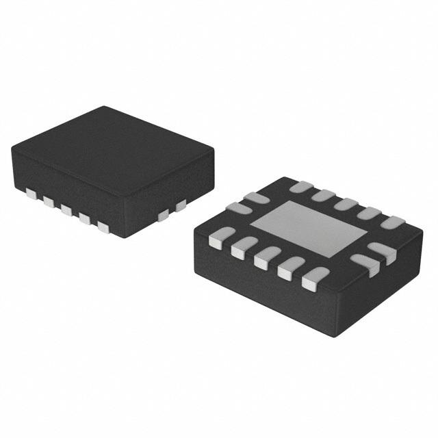
| 产品图片 |
|
| 产品型号 | PI4ULS5V102UEX |
| rohs | 无铅 / 符合限制有害物质指令(RoHS)规范要求 |
| 产品系列 | ULS |
| 传播延迟(最大值) | 4ns |
| 位数 | 2 |
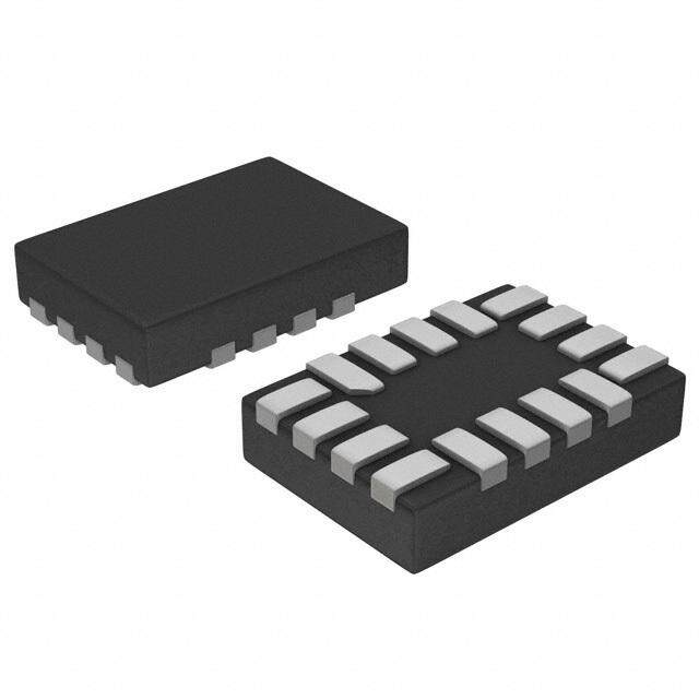
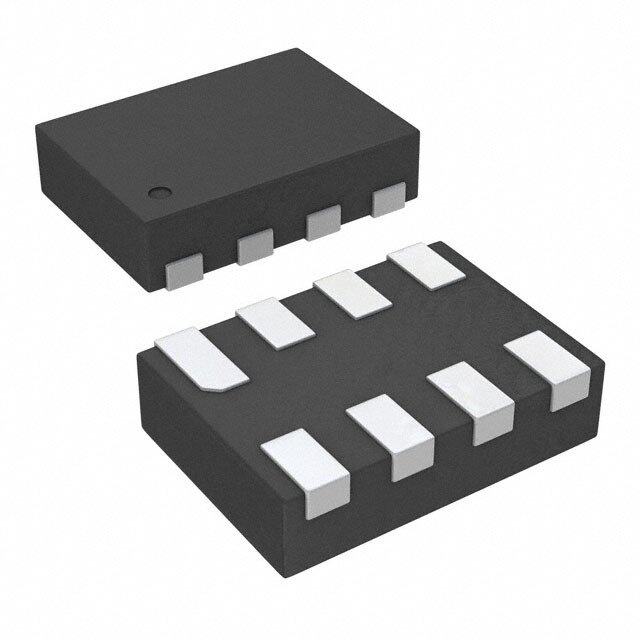
| 供应商器件封装 | 8-MSOP |
| 其它名称 | PI4ULS5V102UEXDKR |
| 包装 | Digi-Reel® |
| 安装类型 | 表面贴装 |
| 封装/外壳 | 8-TSSOP,8-MSOP(0.118",3.00mm 宽) |
| 工作温度 | -40°C ~ 85°C |
| 差分-输入:输出 | 无/无 |
| 数据速率 | 100Mbps |
| 标准包装 | 1 |
| 电压-电源 | 1.2 V ~ 3.6 V,1.65 V ~ 5.5 V |
| 输入类型 | 电压 |
| 输出/通道数 | 1 |
| 输出类型 | 电压 |
| 通道数 | 2 |
| 逻辑功能 | 电平移位器,双向,3 态 |


- 商务部:美国ITC正式对集成电路等产品启动337调查
- 曝三星4nm工艺存在良率问题 高通将骁龙8 Gen1或转产台积电
- 太阳诱电将投资9.5亿元在常州建新厂生产MLCC 预计2023年完工
- 英特尔发布欧洲新工厂建设计划 深化IDM 2.0 战略
- 台积电先进制程称霸业界 有大客户加持明年业绩稳了
- 达到5530亿美元!SIA预计今年全球半导体销售额将创下新高
- 英特尔拟将自动驾驶子公司Mobileye上市 估值或超500亿美元
- 三星加码芯片和SET,合并消费电子和移动部门,撤换高东真等 CEO
- 三星电子宣布重大人事变动 还合并消费电子和移动部门
- 海关总署:前11个月进口集成电路产品价值2.52万亿元 增长14.8%


PDF Datasheet 数据手册内容提取
PI4ULS5V102 2-Bit Universal Bi-directional Level Shifter with Automatic Direction Control & Advance Package Solution Features Description 1.2V to 3.6V on A Port and 1.65V to 5.5V on B Port This 2-bit non-inverting translator uses two separate (VCCA ≤ VCCB) configurable power-supply rails. The A port is designed to VCC Isolation Feature – If Either VCC Input Is at GND, track V . V accepts any supply voltage from 1.2V to 3.6V. CCA CCA All Outputs Are in the High-Impedance State The B port is designed to track V . V accepts any supply CCB CCB OE Input Circuit Referenced to VCCA voltage from 1.65V to 5.5V. This allows for universal Low Power Consumption, 5 μA Max ICC low-voltage bidirectional translation between any of the 1.2V, Ioff Supports Partial-Power-Down Mode Operation 1.5V, 1.8V, 2.5V, 3.3V, and 5V voltage nodes. V should not CCA Latch-Up Performance Exceeds 100mA Per JESD 78, exceed VCCB. Class II When the output-enable (OE) input is low, all outputs are ESD Protection Exceeds JESD 22 placed in the high-impedance state. A Port 2500-V Human-Body Model (A114-F) This device is fully specified for partial-power-down 200-V Machine Model (A115-A) applications using Ioff. The Ioff circuitry disables the outputs, 1500-V Charged-Device Model (C101D) preventing damaging current backflow through the device B Port when it is powered down. 15-kV Human-Body Model (A114-F) To ensure the high-impedance state during power up or 200-V Machine Model (A115-A) power down, OE should be tied to GND through a pull-down 1500-V Charged-Device Model (C101D) resistor; the minimum value of the resistor is determined by the current-sourcing capability of the driver. Pin Assignment Function Block Diagram 1 2 D A2 A1 C VCCA OE B GND VCCB A B2 B1 Pin Description Pin Name Description B1, B2 Input/output B. Referenced to V . CCB GND Ground. A port supply voltage. 1.2 V ≤V ≤ 3.6 V and V CCA CCA V ≤V CCA CCB. A1, A2 Input/output A. Referenced to V CCA. 3-State output. Pull OE low to place all outputs in OE 3-state mode. Referenced to V . CCA V B port supply voltage. 1.65 V ≤V ≤ 5.5 V. MSOP-8 (Top View) CCB CCB PI4ULS5V102 www.diodes.com December 2017 Document Number DS40264 Rev 1-2 1 © Diodes Incorporated
PI4ULS5V102 Maximum Ratings*1 Min Max Unit V -0.5 4.6 CCA Supply voltage range V V -0.5 6.5 CCB A port -0.5 4.6 V Input voltage range V I B port -0.5 6.5 Voltage range applied to any output in the high-impedance or A port -0.5 4.6 V V O power-off state B port -0.5 6.5 A port -0.5 V + 0.5 V Voltage range applied to any output in the high or low state*2 CCA V O B port -0.5 V + 0.5 CCB I Input clamp current, V < 0 -50 mA IK I I Output clamp current, V < 0 -50 mA OK O I Continuous output current ±50 mA O I Continuous current through V , V , or GND ±100 mA O CCA CCB T Storage temperature range -65 150 ℃ stg *1 Stresses greater than those listed under MAXIMUM RATINGS may cause permanent damage to the device. This is a stress rating only and functional operation of the device at these or any other conditions above those indicated in the operational sections of this specification is not implied. Exposure to absolute maximum rating conditions for extended periods may affect reliability. *2 The value of V and V are provided in the recommended operating conditions table. CCA CCB Recommend Operation Conditions (1)(2) Parameter Description V V Min Max Unit CCA CCB V - - 1.2 3.6 CCA Supply voltage V V - - 1.65 5.5 CCB Data 1.2V to 1.65V to V * CCI V inputs 3.6V 5.5V 0.65(3) CCI V High-level input voltage V IH 1.2V to 1.65V to V * OE input CCA 5.5 3.6V 5.5V 0.7 Data 1.2V to 1.65V to V * 0 CCI inputs 3.6V 5.5V 0.35(3) V Low-level input voltage V IL 1.2V to 1.65V to V * OE input 0 CCA 3.6V 5.5V 0.3 Voltage range applied to any output in the A port 1.2V to 1.65V to 0 3.6 V V O high-impedance or power-off state B port 3.6V 5.5V 0 5.5 A port 1.2V to 1.65V to - 40 inputs 3.6V 5.5V 1.65V to △t/△v Input transition rise or fall rate - 40 ns/V B port 1.2V to 3.6V inputs 3.6V 4.5V to - 30 5.5V T Operating free-air temperature - - -40 85 ℃ A (1) The A and B sides of an unused data I/O pair must be held in the same state, i.e., both at V or both at GND. CCI (2) V must be less than or equal to V and must not exceed 3.6 V. CCA CCB (3) V is the supply voltage associated with the input port. CCI PI4ULS5V102 www.diodes.com December 2017 Document Number DS40264 Rev 1-2 2 © Diodes Incorporated
PI4ULS5V102 DC Electrical Characteristics(1)(2) T = 25℃ -40 to 85℃ Parameter Test Conditions V V A Unit CCA CCB Min Typ Max Min Max 1.2V 1.0 1.1 1.2 - - V I = -20μA - V OHA OH V 1.4V to 3.6V - - - CCA - - 0.4 1.2V 0.0 0.09 0.4 - - V V I = 20μA - OLA OL 1.4V to 3.6V - - - - 0.4 V V V I = -20μA - 1.65V to 5.5V - - - CCB OHB OH - 0.4 V I = 20μA - 1.65V to 5.5V - - - - 0.4 V OLB OL V = V or I OE I CCI 1.2 to 3.6V 1.65V to 5.5V - - ±1 - ±2 μA I GND V or V = 0 to A port I O 0V 0V to 5.5V - - ±1 - ±2 3.6V I μA off V or V = 0 to B port I O 0 to 3.6V 0V - - ±1 - ±2 5.5V A or B I OE = GND 1.2 to 3.6V 1.65V to 5.5V - - ±1 - ±2 μA OZ port 1.2V 1.65V to 5.5V 0.0 0.06 5.0 - - V = V or 1.4V to 3.6V 1.65V to 5.5V - - - - 5 I I CCI μA CCA GND, Io = 0 3.6V 0V - - - - 2 0V 5.5V - - - - -2 1.2V 1.65V to 5.5V 0 2.3 5.0 - - V = V or 1.4V to 3.6V 1.65V to 5.5V - - - - 5 I I CCI μA CCB GND, Io = 0 3.6V 0V - - - - -2 0V 5.5V - - - - 2 V = V or 1.2V 1.65V to 5.5V 0.0 2.4 8.0 - - I + I I CCI μA CCA CCB GND, Io = 0 1.4V to 3.6V 1.65V to 5.5V - - - - 8 V = V or 1.2V 1.65V to 5.5V 0.0 0.05 0.4 - - I CCI I GND, Io = 0, OE μA CCZA = GND 1.4V to 3.6V 1.65V to 5.5V - - - - 3 V = V or 1.2V 1.65V to 5.5V 0.0 2.3 5.0 - - I CCI I GND, Io = 0, OE μA CCZB = GND 1.4V to 3.6V 1.65V to 5.5V - - - - 5 Ci OE - 1.2 to 3.6V 1.65V to 5.5V - 2.5 - - 3 pF A port - 5 - - 6 Cio - 1.2 to 3.6V 1.65V to 5.5V pF B port - 11 - - 14 (1) V is the supply voltage associated with the input port. CCI (2) V is the supply voltage associated with the output port. CCO PI4ULS5V102 www.diodes.com December 2017 Document Number DS40264 Rev 1-2 3 © Diodes Incorporated
PI4ULS5V102 AC Electrical Characteristics Timing requirements a. T = 25℃, V = 1.2V A CCA V = 1.8V V = 2.5V V = 3.3V V = 5V CCB CCB CCB CCB Unit TYP TYP TYP TYP Data rate 20 20 20 20 Mbps t Pulse duration Data inputs 50 50 50 50 ns W b. T = 25℃, V = 1.5±0.1V A CCA V =1.8±0.15V V =2.5±0.2V V =3.3±0.3V V =5±0.5V CCB CCB CCB CCB Unit MIN MAX MIN MAX MIN MAX MIN MAX Mbp Data rate - 40 - 40 - 40 - 40 s t Pulse duration Data inputs 25 - 25 - 25 - 25 - ns W c. T = 25℃, V = 1.8±0.15V A CCA V =1.8±0.15V V =2.5±0.2V V =3.3±0.3V V =5±0.5V CCB CCB CCB CCB Unit MIN MAX MIN MAX MIN MAX MIN MAX Data rate - 60 - 60 - 60 - 60 Mbps t Pulse duration Data inputs 17 - 17 - 17 - 17 - ns W d. T = 25℃, V = 2.5±0.2V A CCA V =2.5±0.2V V =3.3±0.3V V =5±0.5V CCB CCB CCB Unit MIN MAX MIN MAX MIN MAX Data rate - 100 - 100 - 100 Mbps t Pulse duration Data inputs 10 - 10 - 10 - ns W e. T = 25℃, V = 3.3±0.3V A CCA V =3.3±0.3V V =5±0.5V CCB CCB Unit MIN MAX MIN MAX Data rate - 100 - 100 Mbps t 10 - 10 - 10 - ns W Switching characteristics a. T = 25℃, V = 1.2V A CCA From To V =1.8V V =2.5V V =3.3V V =5V Parameter CCB CCB CCB CCB Unit (INPUT) (OUTPUT) TYP TYP TYP TYP A B 6.9 5.7 5.3 5.5 t ns pd B A 7.4 6.4 6 5.8 A 0.2 0.2 0.2 0.2 t OE μs en B 0.2 0.2 0.2 0.2 A 0.4 0.4 0.4 0.4 t OE μs dis B 0.2 0.2 0.2 0.2 A-port rise and fall t , t 4.2 4.2 4.2 4.2 ns rA fA times B-port rise and fall t , t 2.1 1.5 1.2 1.1 ns rB fB times Channel-to-channel t 0.5 0.5 0.5 1.4 ns SK(O) skew Max data rate - 20 20 20 20 Mbps PI4ULS5V102 www.diodes.com December 2017 Document Number DS40264 Rev 1-2 4 © Diodes Incorporated
PI4ULS5V102 b. T = 25℃, V = 1.5±0.1V A CCA From To V =1.8±0.15V V = 2.5±0.2V V =3.3±0.3V V = 5±0.5V Parameter CCB CCB CCB CCB Unit (INPUT) (OUTPUT) MIN MAX MIN MAX MIN MAX MIN MAX A B 1.4 12.9 1.2 10.1 1.1 10 0.8 9.9 t ns pd B A 0.9 14.2 0.7 12 0.4 11.7 0.3 13.7 A - 0.5 - 0.5 - 0.5 - 0.5 t OE μs en B - 0.5 - 0.5 - 0.5 - 0.5 A - 0.5 - 0.5 - 0.5 - 0.5 t OE μs dis B - 0.5 - 0.5 - 0.5 - 0.5 A-port rise and fall t , t 1.4 5.1 1.4 5.1 1.4 5.1 1.4 5.1 ns rA fA times B-port rise and fall t , t 0.9 4.5 0.6 3.2 0.5 2.8 0.4 2.7 ns rB fB times Channel-to-channel t - 0.5 - 0.5 - 0.5 - 0.5 ns SK(O) skew Max data rate 40 - 40 - 40 - 40 - Mbps c. T = 25℃, V = 1.8±0.15V A CCA From To V =1.8±0.15V V =2.5±0.2V V =3.3±0.3V V =5±0.5V Parameter CCB CCB CCB CCB Unit (INPUT) (OUTPUT) MIN MAX MIN MAX MIN MAX MIN MAX A B 1.6 11 1.4 7.7 1.3 6.8 1.2 6.5 t ns pd B A 1.5 12 1.3 8.4 1 7.6 0.9 7.1 A - 0.3 - 0.25 0.25 - 0.25 t OE μs en B - 0.3 - 0.25 0.25 - 0.25 A - 0.5 - 0.5 0.5 - 0.5 t OE μs dis B - 0.5 - 0.5 0.5 - 0.5 A-port rise and fall t , t 1 4.2 1 4.1 1 4.1 1 4.1 ns rA fA times B-port rise and fall t , t 0.9 4.5 0.6 3.2 0.5 2.8 0.4 2.7 ns rB fB times Channel-to-channel t - 0.5 - 0.5 - 0.5 - 0.5 ns SK(O) skew Max data rate 60 - 60 - 60 - 60 - Mbps d. T = 25℃, V = 2.5±0.2V A CCA From To V =2.5±0.2V V =3.3±0.3V V =5±0.5V Parameter CCB CCB CCB Unit (INPUT) (OUTPUT) MIN MAX MIN MAX MIN MAX A B 1.1 6.3 1.0 5.2 0.9 4.7 t ns pd B A 1.2 6.6 1.1 5.1 0.9 4.4 A - 0.25 - 0.2 - 0.2 t OE μs en B - 0.25 - 0.2 - 0.2 A - 0.5 - 0.4 - 035 t OE μs dis B - 0.5 - 0.4 - 0.35 t , t A-port rise and fall times 0.8 3.0 0.8 3.0 0.8 3.0 ns rA fA t , t B-port rise and fall times 0.7 3.0 0.5 2.8 0.4 2.7 ns rB fB t Channel-to-channel skew - 0.5 - 0.5 - 0.5 ns SK(O) Max data rate 100 - 100 - 100 - Mbps PI4ULS5V102 www.diodes.com December 2017 Document Number DS40264 Rev 1-2 5 © Diodes Incorporated
PI4ULS5V102 e. T = 25℃, V = 3.3±0.3V A CCA From To V =3.3±0.3V V =5±0.5V Parameter CCB CCB Unit (INPUT) (OUTPUT) MIN MAX MIN MAX A B 0.9 4.7 0.8 4.0 t ns pd B A 1.0 4.9 0.9 3.8 A - 0.2 - 0.2 t OE μs en B - 0.2 - 0.2 A - 0.3 - 0.3 t OE μs dis B - 0.3 - 0.3 t , t A-port rise and fall times 0.7 2.8 0.7 2.8 ns rA fA t , t B-port rise and fall times 0.5 2.7 0.4 2.7 ns rB fB t Channel-to-channel skew - 0.5 - 0.5 ns SK(O) Max data rate 100 - 100 - Mbps Operating characteristics V CCA 1.2V 1.2V 1.5V 1.8V 2.5V 2.5V 3.3V V CCB Parameter Test Conditions 3.3V Unit 5V 1.8V 1.8V 1.8V 2.5V 5V to 5.5V TYP TYP TYP TYP TYP TYP TYP A-port input, B-port output. C =0, f=10 MHz, 7.8 10 9 8 8 8 9 C L pdA B-port input, A-port output. tr = t =1ns, 12 11 11 11 11 11 11 f A-port input, B-port output. OE=V 38.1 28 28 28 29 30 30 C CCA pdB B-port input, A-port output. (outputs enabled) 25.4 18 18 18 18 21 21 pF A-port input, B-port output. C =0, f =10 MHz, 0.01 0.01 0.01 0.01 0.01 0.01 0.01 C L pdA B-port input, A-port output. tr = t =1ns, 0.01 0.01 0.01 0.01 0.01 0.01 0.01 f A-port input, B-port output. OE=GND 0.01 0.01 0.01 0.01 0.01 0.01 0.03 C pdB B-port input, A-port output. (outputs disabled) 0.01 0.01 0.01 0.01 0.01 0.02 0.04 PI4ULS5V102 www.diodes.com December 2017 Document Number DS40264 Rev 1-2 6 © Diodes Incorporated
PI4ULS5V102 Test circuit 1> Load circuit for Max data rate, pulse duration propagation delay output rise and fall time measurement 2> Load circuit for enable/disable time measurement 3> Timing Definitions for Propagation Delays and Enable/Disable Measurement 4> Voltage waveforms pulse duration 5> Notes A. C includes probe and jig capacitance. L B. All input pulses are supplied by generators having the following characteristics: PRR_10 MHz, Z = 50 W, dv/dt ≥ 1 V/ns. O C. The outputs are measured one at a time, with one transition per measurement. D. t and t are the same as tpd. PLH PHL E. V is the V associated with the input port. CCI CC F. V is the V associated with the output port. CCO CC G. All parameters and waveforms are not applicable to all devices. PI4ULS5V102 www.diodes.com December 2017 Document Number DS40264 Rev 1-2 7 © Diodes Incorporated
PI4ULS5V102 Principles of operation Applications The PI4ULS5V102 can be used in level-translation applications for interfacing devices or systems operating at different interface voltages with one another. Architecture The PI4ULS5V102 architecture (see Figure1) does not require a direction-control signal to control the direction of data flow from A to B or from B to A. In a dc state, the output drivers of the PI4ULS5V102 can maintain a high or low, but are designed to be weak, so that they can be overdriven by an external driver when data on the bus starts flowing the opposite direction. The output one shots detect rising or falling edges on the A or B ports. During a rising edge, the one shot turns on the PMOS transistors (T1, T3) for a short duration, which speeds up the low-to-high transition. Similarly, during a falling edge, the one shot turns on the NMOS transistors (T2, T4) for a short duration, which speeds up the high-to-low transition. The typical output impedance during output transition is 70 Ω at V =1.2 V to 1.8 V, 50 Ω at V =1.8 V to 3.3 V, and 40 Ω at V =3.3 V to 5 V. CCO CCO CCO Input Driver Requirements Typical I vs V characteristics of the PI4ULS5V102 are shown in Figure 2. For proper operation, the device driving the data IN IN I/Os of the PI4ULS5V102 must have drive strength of at least ±2mA. Power Up During operation, ensure that V ≤ V at all times. During power-up sequencing, VCCA ≥ VCCB does not damage the device, CCA CCB so any power supply can be ramped up first. The PI4ULS5V102 has circuitry that disables all output ports when either V is CC switched off (V = 0 V). CCA/B Enable and Disable The PI4ULS5V102 has an OE input that is used to disable the device by setting OE = low, which places all I/Os in the high-impedance (Hi-Z) state. The disable time (t ) indicates the delay between when OE goes low and when the outputs acutally dis get disabled (Hi-Z). The enable time (ten) indicates the amount of time the user must allow for the one-shot circuitry to become operational after OE is taken high. Pull-up or Pull-down Resistors on I/O Lines The PI4ULS5V102 is designed to drive capacitive loads of up to 70 pF. The output drivers of the PI4ULS5V102 have low dc drive strength. If pullup or pulldown resistors are connected externally to the data I/Os, their values must be kept higher than 50 kΩ to ensure that they do not contend with the output drivers of the PI4ULS5V102. For the same reason, the PI4ULS5V102 should not be used in applications such as I2C or 1-Wire where an open-drain driver is connected on the bidirectional data I/O. PI4ULS5V102 www.diodes.com December 2017 Document Number DS40264 Rev 1-2 8 © Diodes Incorporated
PI4ULS5V102 Figure 1. Architecture of PI4ULS5V102 I/O Cell Figure 2. Typical I vs V Curve IN IN Note: A. VT is the input threshold voltage of the PI4ULS5V102 (typically V /2). CCI B. VD is the supply voltage of the external driver. PI4ULS5V102 www.diodes.com December 2017 Document Number DS40264 Rev 1-2 9 © Diodes Incorporated
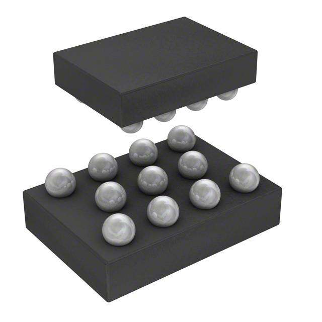
PI4ULS5V102 Mechanical Information CSP-8 PI4ULS5V102 www.diodes.com December 2017 Document Number DS40264 Rev 1-2 10 © Diodes Incorporated
PI4ULS5V102 MSOP-8 8 7 6 5 1 2 3 4 For latest package info. please check: http://www.diodes.com/design/support/packaging/pericom-packaging/packaging-mechanicals-and-thermal-characteristics/ Ordering Information Part Number Package Code Package PI4ULS5V102GAEX GA 8-Pin, 0.95x1.94 Wafer Level (CSP) PI4ULS5V102UEX U 8-Pin, Mini Small Outline Package (MSOP) Notes: Thermal characteristics can be found on the company web site at www.diodes.com/design/support/packaging/ E = Pb-free and Green X suffix = Tape/Reel PI4ULS5V102 www.diodes.com December 2017 Document Number DS40264 Rev 1-2 11 © Diodes Incorporated
PI4ULS5V102 IMPORTANT NOTICE DIODES INCORPORATED MAKES NO WARRANTY OF ANY KIND, EXPRESS OR IMPLIED, WITH REGARDS TO THIS DOCUMENT, INCLUDING, BUT NOT LIMITED TO, THE IMPLIED WARRANTIES OF MERCHANTABILITY AND FITNESS FOR A PARTICULAR PURPOSE (AND THEIR EQUIVALENTS UNDER THE LAWS OF ANY JURISDICTION). Diodes Incorporated and its subsidiaries reserve the right to make modifications, enhancements, improvements, corrections or other changes without further notice to this document and any product described herein. Diodes Incorporated does not assume any liability arising out of the application or use of this document or any product described herein; neither does Diodes Incorporated convey any license under its patent or trademark rights, nor the rights of others. Any Customer or user of this document or products described herein in such applications shall assume all risks of such use and will agree to hold Diodes Incorporated and all the companies whose products are represented on Diodes Incorporated website, harmless against all damages. Diodes Incorporated does not warrant or accept any liability whatsoever in respect of any products purchased through unauthorized sales channel. Should Customers purchase or use Diodes Incorporated products for any unintended or unauthorized application, Customers shall indemnify and hold Diodes Incorporated and its representatives harmless against all claims, damages, expenses, and attorney fees arising out of, directly or indirectly, any claim of personal injury or death associated with such unintended or unauthorized application. Products described herein may be covered by one or more United States, international or foreign patents pending. Product names and markings noted herein may also be covered by one or more United States, international or foreign trademarks. This document is written in English but may be translated into multiple languages for reference. Only the English version of this document is the final and determinative format released by Diodes Incorporated. LIFE SUPPORT Diodes Incorporated products are specifically not authorized for use as critical components in life support devices or systems without the express written approval of the Chief Executive Officer of Diodes Incorporated. As used herein: A. Life support devices or systems are devices or systems which: 1. are intended to implant into the body, or 2. support or sustain life and whose failure to perform when properly used in accordance with instructions for use provided in the labeling can be reasonably expected to result in significant injury to the user. B. A critical component is any component in a life support device or system whose failure to perform can be reasonably expected to cause the failure of the life support device or to affect its safety or effectiveness. Customers represent that they have all necessary expertise in the safety and regulatory ramifications of their life support devices or systems, and acknowledge and agree that they are solely responsible for all legal, regulatory and safety-related requirements concerning their products and any use of Diodes Incorporated products in such safety-critical, life support devices or systems, notwithstanding any devices- or systems-related information or support that may be provided by Diodes Incorporated. Further, Customers must fully indemnify Diodes Incorporated and its representatives against any damages arising out of the use of Diodes Incorporated products in such safety-critical, life support devices or systems. Copyright © 2016, Diodes Incorporated www.diodes.com PI4ULS5V102 www.diodes.com December 2017 Document Number DS40264 Rev 1-2 12 © Diodes Incorporated
Mouser Electronics Authorized Distributor Click to View Pricing, Inventory, Delivery & Lifecycle Information: D iodes Incorporated: PI4ULS5V102UEX