ICGOO在线商城 > 集成电路(IC) > 逻辑 - 缓冲器,驱动器,接收器,收发器 > 74LCXZ16244MTDX

 Datasheet下载
- 型号: 74LCXZ16244MTDX
- 制造商: Fairchild Semiconductor
- 库位|库存: xxxx|xxxx
- 要求:
| 数量阶梯 | 香港交货 | 国内含税 |
| +xxxx | $xxxx | ¥xxxx |
查看当月历史价格
查看今年历史价格
74LCXZ16244MTDX产品简介:
ICGOO电子元器件商城为您提供74LCXZ16244MTDX由Fairchild Semiconductor设计生产,在icgoo商城现货销售,并且可以通过原厂、代理商等渠道进行代购。 74LCXZ16244MTDX价格参考。Fairchild Semiconductor74LCXZ16244MTDX封装/规格:逻辑 - 缓冲器,驱动器,接收器,收发器, 缓冲器,非反向 4 Element 4 Bit per Element 三态 Output 48-TSSOP。您可以下载74LCXZ16244MTDX参考资料、Datasheet数据手册功能说明书,资料中有74LCXZ16244MTDX 详细功能的应用电路图电压和使用方法及教程。
ON Semiconductor的74LCXZ16244MTDX是一款16位缓冲器/驱动器,属于低电压CMOS逻辑系列,具有5V输入兼容和高噪声抑制能力。该器件适用于需要电平转换和信号驱动的数字系统,广泛应用于通信设备、工业控制、消费电子及计算机外设等领域。

典型应用场景包括:在微处理器系统中作为地址或数据总线的缓冲驱动,提升驱动能力并隔离负载影响;用于FPGA或ASIC与外围器件之间的信号接口,实现高速、低功耗的数据传输;在背板系统或多板互联系统中作为线路接收器或收发器,增强信号完整性。

其24引脚TSSOP封装(MTDX)节省空间,适合高密度PCB布局。工作温度范围为-40°C至+85°C,满足工业级环境要求。由于支持3.3V电源供电且兼容5V输入信号,74LCXZ16244MTDX可无缝集成于混合电压系统中,实现不同电压域间的可靠通信。此外,内部上拉电阻设计简化了外部电路,提升了系统稳定性。

综上,该器件适用于需高效信号调理与电平转换的中高密度数字系统,是工业自动化、网络设备及嵌入式系统中的理想选择。
| 参数 | 数值 |
| 产品目录 | 集成电路 (IC) |
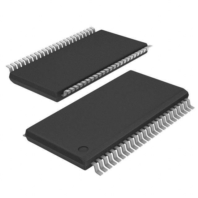
| 描述 | IC BUFF/DVR 16BIT LOW V 48TSSOP |
| 产品分类 | |
| 品牌 | Fairchild Semiconductor |
| 数据手册 | |
| 产品图片 |
|
| 产品型号 | 74LCXZ16244MTDX |
| rohs | 无铅 / 符合限制有害物质指令(RoHS)规范要求 |
| 产品系列 | 74LCXZ |
| 供应商器件封装 | 48-TSSOP |
| 元件数 | 4 |
| 其它名称 | 74LCXZ16244MTDXDKR |
| 包装 | Digi-Reel® |
| 安装类型 | 表面贴装 |
| 封装/外壳 | 48-TFSOP(0.240",6.10mm 宽) |
| 工作温度 | -40°C ~ 85°C |
| 标准包装 | 1 |
| 每元件位数 | 4 |
| 电压-电源 | 2.7 V ~ 3.6 V |
| 电流-输出高,低 | 24mA,24mA |
| 逻辑类型 | 缓冲器/线路驱动器,非反相 |


.jpg)


PDF Datasheet 数据手册内容提取
Is Now Part of To learn more about ON Semiconductor, please visit our website at www.onsemi.com Please note: As part of the Fairchild Semiconductor integration, some of the Fairchild orderable part numbers will need to change in order to meet ON Semiconductor’s system requirements. Since the ON Semiconductor product management systems do not have the ability to manage part nomenclature that utilizes an underscore (_), the underscore (_) in the Fairchild part numbers will be changed to a dash (-). This document may contain device numbers with an underscore (_). Please check the ON Semiconductor website to verify the updated device numbers. The most current and up-to-date ordering information can be found at www.onsemi.com. Please email any questions regarding the system integration to Fairchild_questions@onsemi.com. ON Semiconductor and the ON Semiconductor logo are trademarks of Semiconductor Components Industries, LLC dba ON Semiconductor or its subsidiaries in the United States and/or other countries. ON Semiconductor owns the rights to a number of patents, trademarks, copyrights, trade secrets, and other intellectual property. A listing of ON Semiconductor’s product/patent coverage may be accessed at www.onsemi.com/site/pdf/Patent-Marking.pdf. ON Semiconductor reserves the right to make changes without further notice to any products herein. ON Semiconductor makes no warranty, representation or guarantee regarding the suitability of its products for any particular purpose, nor does ON Semiconductor assume any liability arising out of the application or use of any product or circuit, and specifically disclaims any and all liability, including without limitation special, consequential or incidental damages. Buyer is responsible for its products and applications using ON Semiconductor products, including compliance with all laws, regulations and safety requirements or standards, regardless of any support or applications information provided by ON Semiconductor. “Typical” parameters which may be provided in ON Semiconductor data sheets and/or specifications can and do vary in different applications and actual performance may vary over time. All operating parameters, including “Typicals” must be validated for each customer application by customer’s technical experts. ON Semiconductor does not convey any license under its patent rights nor the rights of others. ON Semiconductor products are not designed, intended, or authorized for use as a critical component in life support systems or any FDA Class 3 medical devices or medical devices with a same or similar classification in a foreign jurisdiction or any devices intended for implantation in the human body. Should Buyer purchase or use ON Semiconductor products for any such unintended or unauthorized application, Buyer shall indemnify and hold ON Semiconductor and its officers, employees, subsidiaries, affiliates, and distributors harmless against all claims, costs, damages, and expenses, and reasonable attorney fees arising out of, directly or indirectly, any claim of personal injury or death associated with such unintended or unauthorized use, even if such claim alleges that ON Semiconductor was negligent regarding the design or manufacture of the part. ON Semiconductor is an Equal Opportunity/Affirmative Action Employer. This literature is subject to all applicable copyright laws and is not for resale in any manner.
7 4 September 2000 L Revised August 2001 C X Z 1 6 74LCXZ16244 2 4 4 Low Voltage 16-Bit Buffer/Line Driver L o with 5V Tolerant Inputs and Outputs w V o General Description Features l t a The LCXZ16244 contains sixteen non-inverting buffers (cid:1)5V tolerant inputs and outputs g woriyth a 3n-dS TaAdTdEre sosu tdpruivtse rd, ecsloigcnke ddr tivoe br,e o er mbpulso yoeride natse da tmraenms-- (cid:1)(cid:1)GSuupapraonrttse elivde p ionwseerrt iuopn//dwoitwhnd rhaiwgha limpedance e 16 mhaitst esre/rpeacreaivtee r3. -TShTeA TdEev cicoen tisro nl iibnbpluet sc ownhtricohll ecda.n E baec hs hnoibrtbeled (cid:1)2.7V–3.6V VCC specifications provided -B together for full 16-bit operation. (cid:1)4.5 ns tPD max (VCC = 3.0V), 20 µA ICC max it B When VCC is between 0 and 1.5V, the LCXZ12644 is in the (cid:1)±24 mA output drive (VCC = 3.0V) u high impedance state during power up or power down. This (cid:1)Implements patented noise/EMI reduction circuitry ff places the outputs in high impedance (Z) state preventing e iennteterdm iattpepnltic laotwio nims.pedance loading or glitching in bus ori- (cid:1)(cid:1)LEaStDch p-ueprf opremrfaonrmcea:nce exceeds 500 mA r/L i The LCXZ16244 is designed for low voltage (2.7V or 3.3V) Human body model > 2000V ne VCC applications with capability of interfacing to a 5V signal Machine model > 200V D environment. (cid:1)Also packaged in plastic Fine-Pitch Ball Grid Array r The LCXZ16244 is fabricated with an advanced CMOS (FBGA) (Preliminary) iv e technology to achieve high speed operation while maintain- r ing CMOS low power dissipation. w it h Ordering Code: 5 V T Order Number Package Number Package Description o 74LCXZ16244GX BGA54A 54-Ball Fine-Pitch Ball Grid Array (FBGA), JEDEC MO-205, 5.5mm Wide le (Note 1) (Preliminary) [TAPE and REEL] r a 74LCXZ16244MEA MS48A 48-Lead Small Shrink Outline Package (SSOP), JEDEC MO-118, 0.300" Wide n (Note 2) t In 74LCXZ16244MTD MTD48 48-Lead Thin Shrink Small Outline Package (TSSOP), JEDEC MO-153, 6.1mm Wide p (Note 2) u t Note 1: BGA package available in Tape and Reel only. s Note 2: Devices also available in Tape and Reel. Specify by appending the suffix letter “X” to the ordering code. a n Logic Symbol d O u t p u t s © 2001 Fairchild Semiconductor Corporation DS500252 www.fairchildsemi.com
4 4 Connection Diagrams Pin Descriptions 2 6 1 Z Pin Assignment for SSOP and TSSOP Pin Names Description X C OEn Output Enable Input (Active LOW) L 4 I0–I15 Inputs 7 O0–O15 Outputs NC No Connect FBGA Pin Assignments 1 2 3 4 5 6 A O0 NC OE1 OE2 NC I0 B O2 O1 NC NC I1 I2 C O4 O3 VCC VCC I3 I4 D O6 O5 GND GND I5 I6 E O8 O7 GND GND I7 I8 F O10 O9 GND GND I9 I10 G O12 O11 VCC VCC I11 I12 H O14 O13 NC NC I13 I14 J O15 NC OE4 OE3 NC I15 Truth Tables Inputs Outputs OE1 I0–I3 O0–O3 L L L Pin Assignment for FBGA L H H H X Z Inputs Outputs OE2 I4–I7 O4–O7 L L L L H H H X Z Inputs Outputs OE3 I8–I11 O8–O11 L L L (Top Thru View) L H H H X Z Inputs Outputs OE4 I12–I15 O12–O15 L L L L H H H X Z H = HIGH Voltage Level L = LOW Voltage Level X = Immaterial Z = High Impedance www.fairchildsemi.com 2
7 Functional Description 4 L The LCXZ16244 contains sixteen non-inverting buffers 3-STATE outputs are controlled by an Output Enable (OEn) CX with 3-STATE standard outputs. The device is nibble input for each nibble. When OEn is LOW, the outputs are in Z (b4utb itins)d ecpoenntrdoellnetd owf itthh ee aocthh enri.b bTlhee f ucnocntitoronli npgi nids ecnatinca lblye, 2-state mode. When OEn is HIGH, the outputs are in the 16 shorted together to obtain full 16-bit operation. The high impedance mode, but this does not interfere with 2 entering new data into the inputs. 4 4 Logic Diagram 3 www.fairchildsemi.com
4 4 Absolute Maximum Ratings 2 (Note 3) 6 1 Symbol Parameter Value Conditions Units Z X VCC Supply Voltage −0.5 to +7.0 V LC VI DC Input Voltage −0.5 to +7.0 V 74 VO DC Output Voltage −0.−50 t.o5 VtoC +C7 +.0 0.5 OOuuttppuutt iinn 3H-ISGTHA ToEr L oOr WVC SCt a=t e0 –(1N.o5tVe 4) V IIK DC Input Diode Current −50 VI < GND mA IOK DC Output Diode Current −50 VO < GND mA +50 VO > VCC IO DC Output Source/Sink Current ±50 mA ICC DC Supply Current per Supply Pin ±100 mA IGND DC Ground Current per Ground Pin ±100 mA TSTG Storage Temperature −65 to +150 °C Recommended Operating Conditions (Note 5) Symbol Parameter Min Max Units VCC Supply Voltage Operating 2.7 3.6 V VI Input Voltage 0 5.5 V VO Output Voltage HIGH or LOW State 0 VCC V 3-STATE or VCC = OFF 0 5.5 IOH/IOL Output Current VCC = 3.0V − 3.6V ±24 mA VCC = 2.7V − 3.0V ±12 TA Free-Air Operating Temperature −40 85 °C ∆t/∆V Input Edge Rate, VIN = 0.8V–2.0V, VCC = 3.0V 0 10 ns/V Note 3: The Absolute Maximum Ratings are those values beyond which the safety of the device cannot be guaranteed. The device should not be operated at these limits. The parametric values defined in the Electrical Characteristics tables are not guaranteed at the Absolute Maximum Ratings. The “Recom- mended Operating Conditions” table will define the conditions for actual device operation. Note 4: IO Absolute Maximum Rating must be observed. Note 5: Unused inputs must be held HIGH or LOW. They may not float. DC Electrical Characteristics VCC TA = −40°C to +85°C Symbol Parameter Conditions Units (V) Min Max VIH HIGH Level Input Voltage 2.7 − 3.6 2.0 V VIL LOW Level Input Voltage 2.7 − 3.6 0.8 V VOH HIGH Level Output Voltage IOH = −100 µA 2.7 − 3.6 VCC − 0.2 IOH = −12 mA 2.7 2.2 V IOH = −18 mA 3.0 2.4 IOH = −24 mA 3.0 2.2 VOL LOW Level Output Voltage IOL = 100 µA 2.7 − 3.6 0.2 IOL = 12 mA 2.7 0.4 V IOL = 16 mA 3.0 0.4 IOL = 24 mA 3.0 0.55 II Input Leakage Current 0 ≤ VI ≤ 5.5V 2.7 − 3.6 ±5.0 µA IOZ 3-STATE Output Leakage 0 ≤ VO ≤ 5.5V 2.7 − 3.6 ±5.0 µA VI = VIH or VIL IOFF Power-Off Leakage Current VI or VO = 5.5V 0 10 µA IPU/PD Power Up/Down VO = 0.5V to VCC 0 − 1.5 ±5.0 µA 3-STATE Output Current VI = GND or VCC ICC Quiescent Supply Current VI = VCC or GND 2.7 − 3.6 225 µA 3.6V ≤ VI, VO ≤ 5.5V (Note 6) 2.7 − 3.6 ±225 ∆ICC Increase in ICC per Input VIH = VCC −0.6V 2.7 − 3.6 500 µA Note 6: Outputs disabled or 3-STATE only. www.fairchildsemi.com 4
7 AC Electrical Characteristics 4 L C TA = −40°C to +85°C, RL = 500 Ω X Symbol Parameter VCC = 3.3V ± 0.3V VCC = 2.7V Units Z1 CL = 50 pF CL = 50 pF 62 Min Max Min Max 4 4 tPHL Propagation Delay 1.0 4.5 1.0 5.2 ns tPLH Data to Output 1.0 4.5 1.0 5.2 tPZL Output Enable Time 1.0 5.5 1.0 6.3 ns tPZH 1.0 5.5 1.0 6.3 tPLZ Output Disable Time 1.0 5.4 1.0 5.7 ns tPHZ 1.0 5.4 1.0 5.7 tOSHL Output to Output Skew (Note 7) 1.0 ns tOSLH 1.0 Note 7: Skew is defined as the absolute value of the difference between the actual propagation delay for any two separate outputs of the same device. The specification applies to any outputs switching in the same direction, either HIGH-to-LOW (tOSHL) or LOW-to-HIGH (tOSLH). Parameter guaranteed by design. Dynamic Switching Characteristics VCC TA = 25°C Symbol Parameter Conditions Units (V) Typical VOLP Quiet Output Dynamic Peak VOL CL = 50 pF, VIH = 3.3V, VIL = 0V 3.3 0.8 V VOLV Quiet Output Dynamic Valley VOL CL = 50 pF, VIH = 3.3V, VIL = 0V 3.3 −0.8 V Capacitance Symbol Parameter Conditions Typical Units CIN Input Capacitance VCC = Open, VI = 0V or VCC 7 pF COUT Output Capacitance VCC = 3.3V, VI = 0V or VCC 8 pF CPD Power Dissipation Capacitance VCC = 3.3V, VI = 0V or VCC, f = 10 MHz 20 pF 5 www.fairchildsemi.com
4 4 AC LOADING and WAVEFORMS 2 Generic for LCX Family 6 1 Z X C L 4 7 FIGURE 1. AC Test Circuit (CL includes probe and jig capacitance) VI CL 6V for VCC = 3.3V, 2.7V 50 pF Waveform for Inverting and Non-Inverting Functions 3-STATE Output High Enable and Disable Times for Logic Propagation Delay. Pulse Width and trec Waveforms Setup Time, Hold Time and Recovery Time for Logic 3-STATE Output Low Enable and trise and tfall Disable Times for Logic FIGURE 2. Waveforms (Input Characteristics; f = 1 MHz, tr = tf = 3 ns) VCC Symbol 3.3V ± 0.3V 2.7V Vmi 1.5V 1.5V Vmo 1.5V 1.5V Vx VOL + 0.3V VOL + 0.3V Vy VOH − 0.3V VOH − 0.3V www.fairchildsemi.com 6
7 Schematic Diagram 4 Generic for LCX Family L C X Z 1 6 2 4 4 7 www.fairchildsemi.com
4 4 Physical Dimensions 2 inches (millimeters) unless otherwise noted 6 1 Z X C L 4 7 54-Ball Fine-Pitch Ball Grid Array (FBGA), JEDEC MO-205, 5.5mm Wide Package Number BGA54A Preliminary www.fairchildsemi.com 8
7 Physical Dimensions 4 inches (millimeters) unless otherwise noted (Continued) L C X Z 1 6 2 4 4 48-Lead Small Shrink Outline Package (SSOP), JEDEC MO-118, 0.300" Wide Package Number MS48A 9 www.fairchildsemi.com
s t Physical Dimensions u inches (millimeters) unless otherwise noted (Continued) p t u O d n a s t u p n I t n a r e l o T V 5 h t i w r e v i r D e n Li / r e f f u B t i B - 6 1 e g a t l o V w o L 4 4 2 6 1 Z X C 48-Lead Thin Shrink Small Outline Package (TSSOP), JEDEC MO-153, 6.1mm Wide L Package Number MTD48 4 7 Fairchild does not assume any responsibility for use of any circuitry described, no circuit patent licenses are implied and Fairchild reserves the right at any time without notice to change said circuitry and specifications. LIFE SUPPORT POLICY FAIRCHILD’S PRODUCTS ARE NOT AUTHORIZED FOR USE AS CRITICAL COMPONENTS IN LIFE SUPPORT DEVICES OR SYSTEMS WITHOUT THE EXPRESS WRITTEN APPROVAL OF THE PRESIDENT OF FAIRCHILD SEMICONDUCTOR CORPORATION. As used herein: 1. Life support devices or systems are devices or systems 2. A critical component in any component of a life support which, (a) are intended for surgical implant into the device or system whose failure to perform can be rea- body, or (b) support or sustain life, and (c) whose failure sonably expected to cause the failure of the life support to perform when properly used in accordance with device or system, or to affect its safety or effectiveness. instructions for use provided in the labeling, can be rea- sonably expected to result in a significant injury to the www.fairchildsemi.com user. www.fairchildsemi.com 10
ON Semiconductor and are trademarks of Semiconductor Components Industries, LLC dba ON Semiconductor or its subsidiaries in the United States and/or other countries. ON Semiconductor owns the rights to a number of patents, trademarks, copyrights, trade secrets, and other intellectual property. A listing of ON Semiconductor’s product/patent coverage may be accessed at www.onsemi.com/site/pdf/Patent−Marking.pdf. ON Semiconductor reserves the right to make changes without further notice to any products herein. ON Semiconductor makes no warranty, representation or guarantee regarding the suitability of its products for any particular purpose, nor does ON Semiconductor assume any liability arising out of the application or use of any product or circuit, and specifically disclaims any and all liability, including without limitation special, consequential or incidental damages. Buyer is responsible for its products and applications using ON Semiconductor products, including compliance with all laws, regulations and safety requirements or standards, regardless of any support or applications information provided by ON Semiconductor. “Typical” parameters which may be provided in ON Semiconductor data sheets and/or specifications can and do vary in different applications and actual performance may vary over time. All operating parameters, including “Typicals” must be validated for each customer application by customer’s technical experts. ON Semiconductor does not convey any license under its patent rights nor the rights of others. ON Semiconductor products are not designed, intended, or authorized for use as a critical component in life support systems or any FDA Class 3 medical devices or medical devices with a same or similar classification in a foreign jurisdiction or any devices intended for implantation in the human body. Should Buyer purchase or use ON Semiconductor products for any such unintended or unauthorized application, Buyer shall indemnify and hold ON Semiconductor and its officers, employees, subsidiaries, affiliates, and distributors harmless against all claims, costs, damages, and expenses, and reasonable attorney fees arising out of, directly or indirectly, any claim of personal injury or death associated with such unintended or unauthorized use, even if such claim alleges that ON Semiconductor was negligent regarding the design or manufacture of the part. ON Semiconductor is an Equal Opportunity/Affirmative Action Employer. This literature is subject to all applicable copyright laws and is not for resale in any manner. PUBLICATION ORDERING INFORMATION LITERATURE FULFILLMENT: N. American Technical Support: 800−282−9855 Toll Free ON Semiconductor Website: www.onsemi.com Literature Distribution Center for ON Semiconductor USA/Canada 19521 E. 32nd Pkwy, Aurora, Colorado 80011 USA Europe, Middle East and Africa Technical Support: Order Literature: http://www.onsemi.com/orderlit Phone: 303−675−2175 or 800−344−3860 Toll Free USA/Canada Phone: 421 33 790 2910 Fax: 303−675−2176 or 800−344−3867 Toll Free USA/Canada Japan Customer Focus Center For additional information, please contact your local Email: orderlit@onsemi.com Phone: 81−3−5817−1050 Sales Representative © Semiconductor Components Industries, LLC www.onsemi.com www.onsemi.com 1
Mouser Electronics Authorized Distributor Click to View Pricing, Inventory, Delivery & Lifecycle Information: O N Semiconductor: 74LCXZ16244MTDX 74LCXZ16244MTD