ICGOO在线商城 > 集成电路(IC) > 时钟/计时 - 时钟发生器,PLL,频率合成器 > 74HC4046AD,653
 Datasheet下载
- 型号: 74HC4046AD,653
- 制造商: NXP Semiconductors
- 库位|库存: xxxx|xxxx
- 要求:
| 数量阶梯 | 香港交货 | 国内含税 |
| +xxxx | $xxxx | ¥xxxx |
查看当月历史价格
查看今年历史价格
74HC4046AD,653产品简介:
ICGOO电子元器件商城为您提供74HC4046AD,653由NXP Semiconductors设计生产,在icgoo商城现货销售,并且可以通过原厂、代理商等渠道进行代购。 74HC4046AD,653价格参考¥1.88-¥4.06。NXP Semiconductors74HC4046AD,653封装/规格:时钟/计时 - 时钟发生器,PLL,频率合成器, 。您可以下载74HC4046AD,653参考资料、Datasheet数据手册功能说明书,资料中有74HC4046AD,653 详细功能的应用电路图电压和使用方法及教程。
Nexperia USA Inc.生产的74HC4046AD,653是一款属于时钟/计时类别下的时钟发生器、PLL(锁相环)和频率合成器的集成电路。该型号的主要应用场景包括:

1. 信号生成与同步:
   74HC4046AD,653可以用于生成精确的时钟信号,适用于需要同步多个模块或设备的应用场景,例如音频处理、数据传输系统以及通信设备中的时钟同步。

2. 频率调制与解调:
   由于其内置了PLL电路,这款芯片非常适合用于频率调制(FM)和解调的应用,例如无线通信系统、遥控器和传感器信号处理。

3. 电机控制与伺服系统:
   在电机控制中,该芯片可用于生成PWM(脉宽调制)信号或作为反馈控制系统的一部分,实现速度和位置的精确控制。

4. 消费电子设备:
   如DVD播放器、电视、音响设备等,需要稳定的时钟源以确保音频和视频信号的同步输出,74HC4046AD,653能够满足此类需求。

5. 工业自动化与测量仪器:
   在工业领域,该芯片可用于数据采集系统、传感器接口和自动化控制设备中,提供精确的时钟信号和频率调节功能。

6. 通信与时钟恢复:
   在串行通信系统中,该芯片可用于时钟信号的恢复和再生,确保数据传输的稳定性和准确性。

总体而言,74HC4046AD,653凭借其多功能性(包含振荡器、相位比较器和分频器),广泛应用于需要精确频率控制和信号同步的各种电子系统中。
| 参数 | 数值 |
| 产品目录 | 集成电路 (IC)半导体 |
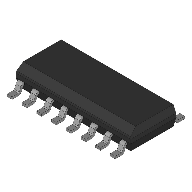
| 描述 | IC PHASE LOCK LOOP W/VCO 16SOIC锁相环 - PLL PHASE LOCKED LOOP W/VCO |
| 产品分类 | |
| 品牌 | NXP Semiconductors |
| 产品手册 | |
| 产品图片 |
|
| rohs | 符合RoHS无铅 / 符合限制有害物质指令(RoHS)规范要求 |
| 产品系列 | RF集成电路,锁相环 - PLL,NXP Semiconductors 74HC4046AD,65374HC |
| 数据手册 | |
| 产品型号 | 74HC4046AD,653 |
| PCN封装 | |
| PCN组件/产地 | |
| PLL | 是 |
| 产品种类 | 锁相环 - PLL |
| 供应商器件封装 | 16-SO |
| 其它名称 | 568-8149-1 |
| 分频器/倍频器 | 无/无 |
| 包装 | 剪切带 (CT) |
| 商标 | NXP Semiconductors |
| 安装类型 | 表面贴装 |
| 安装风格 | SMD/SMT |
| 封装 | Reel |
| 封装/外壳 | 16-SOIC(0.154",3.90mm 宽) |
| 封装/箱体 | SO-16 |
| 工作温度 | -40°C ~ 125°C |
| 工作电源电压 | 5 V |
| 工厂包装数量 | 2500 |
| 差分-输入:输出 | 无/无 |
| 最大工作温度 | + 125 C |
| 最小工作温度 | - 40 C |
| 标准包装 | 1 |
| 比率-输入:输出 | 2:3 |
| 电压-电源 | 3 V ~ 6 V |
| 电源电压-最大 | 6 V |
| 电源电压-最小 | 2 V |
| 电路数 | 1 |
| 电路数量 | 1 |
| 类型 | 锁相环路(PLL) |
| 输入 | 时钟 |
| 输出 | 时钟 |
| 零件号别名 | 74HC4046AD-T |
| 频率-最大值 | 21MHz |


- 商务部:美国ITC正式对集成电路等产品启动337调查
- 曝三星4nm工艺存在良率问题 高通将骁龙8 Gen1或转产台积电
- 太阳诱电将投资9.5亿元在常州建新厂生产MLCC 预计2023年完工
- 英特尔发布欧洲新工厂建设计划 深化IDM 2.0 战略
- 台积电先进制程称霸业界 有大客户加持明年业绩稳了
- 达到5530亿美元!SIA预计今年全球半导体销售额将创下新高
- 英特尔拟将自动驾驶子公司Mobileye上市 估值或超500亿美元
- 三星加码芯片和SET,合并消费电子和移动部门,撤换高东真等 CEO
- 三星电子宣布重大人事变动 还合并消费电子和移动部门
- 海关总署:前11个月进口集成电路产品价值2.52万亿元 增长14.8%


PDF Datasheet 数据手册内容提取
74HC4046A; 74HCT4046A Phase-locked loop with VCO Rev. 3 — 8 June 2016 Product data sheet 1. General description The 74HC4046A; 74HCT4046A is a high-speed Si-gate CMOS device. It is specified in compliance with JEDEC standard no7A. 2. Features and benefits Low power consumption VCO-Inhibit control for ON/OFF keying and for low standby power consumption Center frequency up to 17MHz(typical) at V =4.5V CC Choice of three phase comparators: PC1: EXCLUSIVE-OR PC2: Edge-triggered J-K flip-flop PC3: Edge-triggered RS flip-flop Excellent Voltage Controlled Oscillator (VCO) linearity Low frequency drift with supply voltage and temperature variations Operating power supply voltage range: VCO section 3.0 V to 6.0V Digital section 2.0 V to 6.0V Zero voltage offset due to operational amplifier buffering ESD protection: HBM JESD22-A114F exceeds 2000V MM JESD22-A115-A exceeds 200V 3. Applications FM modulation and demodulation Frequency synthesis and multiplication Frequency discrimination Tone decoding Data synchronization and conditioning Voltage-to-frequency conversion Motor-speed control
74HC4046A; 74HCT4046A Nexperia Phase-locked loop with VCO 4. Ordering information Table 1. Ordering info rmation Type number Package Name Description Version 74HC4046AD SO16 plastic small outline package; 16 leads; body width 3.9 mm SOT109-1 74HCT4046AD 74HC4046ADB SSOP16 plastic shrink small outline package; 16 leads; body width 5.3 mm SOT338-1 74HCT4046ADB 74HC4046APW TSSOP16 plastic thin shrink small outline package; 16 leads; body width 4.4 mm SOT403-1 5. Block diagram (cid:38)(cid:20) (cid:25) (cid:26) (cid:23) (cid:22) (cid:20)(cid:23) (cid:38)(cid:20)(cid:36) (cid:38)(cid:20)(cid:37) (cid:57)(cid:38)(cid:50)(cid:66)(cid:50)(cid:56)(cid:55) (cid:38)(cid:50)(cid:48)(cid:51)(cid:66)(cid:44)(cid:49) (cid:54)(cid:44)(cid:42)(cid:66)(cid:44)(cid:49) (cid:23)(cid:19)(cid:23)(cid:25)(cid:36) (cid:53)(cid:21) (cid:20)(cid:21) (cid:51)(cid:43)(cid:36)(cid:54)(cid:40) (cid:51)(cid:38)(cid:20)(cid:66)(cid:50)(cid:56)(cid:55) (cid:21) (cid:38)(cid:50)(cid:48)(cid:51)(cid:36)(cid:53)(cid:36)(cid:55)(cid:50)(cid:53) (cid:20) (cid:53)(cid:21) (cid:57)(cid:38)(cid:50) (cid:51)(cid:38)(cid:21)(cid:66)(cid:50)(cid:56)(cid:55) (cid:20)(cid:22) (cid:53)(cid:20) (cid:20)(cid:20) (cid:51)(cid:43)(cid:36)(cid:54)(cid:40) (cid:53)(cid:22) (cid:38)(cid:50)(cid:48)(cid:51)(cid:36)(cid:53)(cid:36)(cid:55)(cid:50)(cid:53) (cid:51)(cid:38)(cid:51)(cid:66)(cid:50)(cid:56)(cid:55) (cid:20) (cid:21) (cid:53)(cid:20) (cid:53)(cid:23) (cid:51)(cid:43)(cid:36)(cid:54)(cid:40) (cid:51)(cid:38)(cid:22)(cid:66)(cid:50)(cid:56)(cid:55) (cid:20)(cid:24) (cid:38)(cid:50)(cid:48)(cid:51)(cid:36)(cid:53)(cid:36)(cid:55)(cid:50)(cid:53) (cid:38)(cid:21) (cid:22) (cid:24) (cid:20)(cid:19) (cid:28) (cid:44)(cid:49)(cid:43) (cid:39)(cid:40)(cid:48)(cid:66)(cid:50)(cid:56)(cid:55) (cid:57)(cid:38)(cid:50)(cid:66)(cid:44)(cid:49) (cid:53)(cid:54) (cid:68)(cid:68)(cid:68)(cid:16)(cid:19)(cid:21)(cid:19)(cid:21)(cid:19)(cid:20) Fig 1. Block diagram 74HC_HCT4046A All information provided in this document is subject to legal disclaimers. © Nexperia B.V. 2017. All rights reserved Product data sheet Rev. 3 — 8 June 2016 2 of 50
74HC4046A; 74HCT4046A Nexperia Phase-locked loop with VCO 6. Functional diagram (cid:21) (cid:51)(cid:38)(cid:20)(cid:66)(cid:50)(cid:56)(cid:55) (cid:38)(cid:50)(cid:48)(cid:51)(cid:66)(cid:44)(cid:49) (cid:22) (cid:20)(cid:24) (cid:51)(cid:38)(cid:22)(cid:66)(cid:50)(cid:56)(cid:55) (cid:145) (cid:20)(cid:22) (cid:51)(cid:38)(cid:21)(cid:66)(cid:50)(cid:56)(cid:55) (cid:21) (cid:51)(cid:38)(cid:20)(cid:66)(cid:50)(cid:56)(cid:55) (cid:54)(cid:44)(cid:42)(cid:66)(cid:44)(cid:49) (cid:20)(cid:23) (cid:20) (cid:51)(cid:38)(cid:51)(cid:66)(cid:50)(cid:56)(cid:55) (cid:54)(cid:44)(cid:42)(cid:66)(cid:44)(cid:49) (cid:20)(cid:23) (cid:20)(cid:22) (cid:51)(cid:38)(cid:21)(cid:66)(cid:50)(cid:56)(cid:55) (cid:38)(cid:50)(cid:48)(cid:51)(cid:66)(cid:44)(cid:49) (cid:22) (cid:20)(cid:24) (cid:51)(cid:38)(cid:22)(cid:66)(cid:50)(cid:56)(cid:55) (cid:38)(cid:20)(cid:36) (cid:25) (cid:38)(cid:20)(cid:36) (cid:25) (cid:20) (cid:51)(cid:38)(cid:51)(cid:66)(cid:50)(cid:56)(cid:55) (cid:38)(cid:20)(cid:37) (cid:26) (cid:38)(cid:20)(cid:37) (cid:26) (cid:23)(cid:19)(cid:23)(cid:25)(cid:36) (cid:23) (cid:57)(cid:38)(cid:50)(cid:66)(cid:50)(cid:56)(cid:55) (cid:53)(cid:20) (cid:20)(cid:20) (cid:53)(cid:20) (cid:20)(cid:20) (cid:154) (cid:57)(cid:38)(cid:50) (cid:20)(cid:19) (cid:39)(cid:40)(cid:48)(cid:66)(cid:50)(cid:56)(cid:55) (cid:53)(cid:21) (cid:20)(cid:21) (cid:53)(cid:21) (cid:20)(cid:21) (cid:20)(cid:19) (cid:39)(cid:40)(cid:48)(cid:66)(cid:50)(cid:56)(cid:55) (cid:154) (cid:6) (cid:57)(cid:38)(cid:50)(cid:66)(cid:44)(cid:49) (cid:28) (cid:57)(cid:38)(cid:50)(cid:66)(cid:44)(cid:49) (cid:28) (cid:23) (cid:57)(cid:38)(cid:50)(cid:66)(cid:50)(cid:56)(cid:55) (cid:6) (cid:44)(cid:49)(cid:43) (cid:24) (cid:44)(cid:49)(cid:43) (cid:24) (cid:68)(cid:68)(cid:68)(cid:16)(cid:19)(cid:21)(cid:19)(cid:21)(cid:19)(cid:21) (cid:68)(cid:68)(cid:68)(cid:16)(cid:19)(cid:21)(cid:19)(cid:21)(cid:19)(cid:22) Fig 2. Logic symbol Fig 3. IEC logic symbol (cid:38)(cid:20) (cid:25) (cid:26) (cid:23) (cid:22) (cid:20)(cid:23) (cid:38)(cid:20)(cid:36) (cid:38)(cid:20)(cid:37) (cid:57)(cid:38)(cid:50)(cid:66)(cid:50)(cid:56)(cid:55) (cid:38)(cid:50)(cid:48)(cid:51)(cid:66)(cid:44)(cid:49) (cid:54)(cid:44)(cid:42)(cid:66)(cid:44)(cid:49) (cid:51)(cid:38)(cid:20)(cid:66)(cid:50)(cid:56)(cid:55) (cid:21) (cid:53)(cid:21) (cid:20)(cid:21) (cid:57)(cid:85)(cid:72)(cid:73) (cid:57)(cid:38)(cid:50) (cid:53)(cid:21) (cid:54)(cid:39) (cid:51)(cid:38)(cid:22)(cid:66)(cid:50)(cid:56)(cid:55) (cid:20)(cid:24) (cid:53)(cid:20) (cid:20)(cid:20) (cid:52) (cid:52) (cid:53)(cid:20) (cid:53)(cid:39) (cid:39)(cid:40)(cid:48)(cid:66)(cid:50)(cid:56)(cid:55) (cid:20)(cid:19) (cid:56)(cid:51) (cid:57)(cid:38)(cid:38) (cid:67)(cid:20)(cid:10) (cid:39) (cid:52) (cid:51) (cid:53)(cid:54) (cid:38)(cid:51) (cid:53)(cid:39)(cid:52) (cid:20)(cid:22) (cid:51)(cid:38)(cid:21)(cid:66)(cid:50)(cid:56)(cid:55) (cid:53)(cid:22) (cid:49) (cid:67)(cid:20)(cid:10) (cid:39) (cid:52) (cid:53)(cid:23) (cid:38)(cid:51) (cid:52) (cid:39)(cid:50)(cid:58)(cid:49) (cid:42)(cid:49)(cid:39)(cid:20) (cid:51)(cid:38)(cid:51)(cid:66)(cid:50)(cid:56)(cid:55) (cid:38)(cid:21) (cid:53)(cid:39) (cid:24) (cid:28) (cid:44)(cid:49)(cid:43) (cid:57)(cid:38)(cid:50)(cid:66)(cid:44)(cid:49) (cid:68)(cid:68)(cid:68)(cid:16)(cid:19)(cid:21)(cid:19)(cid:21)(cid:19)(cid:23) Fig 4. Logic diagram 74HC_HCT4046A All information provided in this document is subject to legal disclaimers. © Nexperia B.V. 2017. All rights reserved Product data sheet Rev. 3 — 8 June 2016 3 of 50
74HC4046A; 74HCT4046A Nexperia Phase-locked loop with VCO 7. Pinning information 7.1 Pinning (cid:26)(cid:23)(cid:43)(cid:38)(cid:23)(cid:19)(cid:23)(cid:25)(cid:36) (cid:26)(cid:23)(cid:43)(cid:38)(cid:55)(cid:23)(cid:19)(cid:23)(cid:25)(cid:36) (cid:51)(cid:38)(cid:51)(cid:66)(cid:50)(cid:56)(cid:55) (cid:20) (cid:20)(cid:25) (cid:57)(cid:38)(cid:38) (cid:51)(cid:38)(cid:20)(cid:66)(cid:50)(cid:56)(cid:55) (cid:21) (cid:20)(cid:24) (cid:51)(cid:38)(cid:22)(cid:66)(cid:50)(cid:56)(cid:55) (cid:38)(cid:50)(cid:48)(cid:51)(cid:66)(cid:44)(cid:49) (cid:22) (cid:20)(cid:23) (cid:54)(cid:44)(cid:42)(cid:66)(cid:44)(cid:49) (cid:57)(cid:38)(cid:50)(cid:66)(cid:50)(cid:56)(cid:55) (cid:23) (cid:20)(cid:22) (cid:51)(cid:38)(cid:21)(cid:66)(cid:50)(cid:56)(cid:55) (cid:44)(cid:49)(cid:43) (cid:24) (cid:20)(cid:21) (cid:53)(cid:21) (cid:38)(cid:20)(cid:36) (cid:25) (cid:20)(cid:20) (cid:53)(cid:20) (cid:38)(cid:20)(cid:37) (cid:26) (cid:20)(cid:19) (cid:39)(cid:40)(cid:48)(cid:66)(cid:50)(cid:56)(cid:55) (cid:42)(cid:49)(cid:39) (cid:27) (cid:28) (cid:57)(cid:38)(cid:50)(cid:66)(cid:44)(cid:49) (cid:68)(cid:68)(cid:68)(cid:16)(cid:19)(cid:21)(cid:19)(cid:21)(cid:19)(cid:24) Fig 5. Pin configuration 7.2 Pin description Table 2. Pin descripti on Symbol Pin Description PCP_OUT 1 phase comparator pulse output PC1_OUT 2 phase comparator 1 output COMP_IN 3 comparator input VCO_OUT 4 VCO output INH 5 inhibit input C1A 6 capacitor C1 connection A C1B 7 capacitor C1 connection B GND 8 ground (0 V) VCO_IN 9 VCO input DEM_OUT 10 demodulator output R1 11 resistor R1 connection R2 12 resistor R2 connection PC2_OUT 13 phase comparator 2 output SIG_IN 14 signal input PC3_OUT 15 phase comparator 3 output V 16 supply voltage CC 74HC_HCT4046A All information provided in this document is subject to legal disclaimers. © Nexperia B.V. 2017. All rights reserved Product data sheet Rev. 3 — 8 June 2016 4 of 50
74HC4046A; 74HCT4046A Nexperia Phase-locked loop with VCO 8. Functional description The 74HC4046A; 74HCT4046A is a phase-locked-loop circuit that comprises a linear voltage-controlled oscillator (VCO) and three different phase comparators (PC1, PC2 and PC3). It has a common signal input amplifier and a common comparator input (see Figure1). Thesignal input can be directly coupled to a large voltage signal, or indirectly coupled (with a series capacitor) to a small voltage signal. A self-bias input circuit keeps small voltage signals within the linear region of the input amplifiers. With a passive low-pass filter, the 74HC4046A; 74HCT4046A forms a second-order loop PLL. The excellent VCO linearity is achieved by the use of linear op amp techniques. 8.1 VCO The VCO requires one external capacitor C1 (between pinsC1A and C1B) and one external resistor R1 (between pinsR1 and GND). Alternatively, it requires two external resistors R1 and R2 (between pinsR1 and GND, and R2 and GND). ResistorR1 and capacitor C1 determine the frequency range of the VCO. Resistor R2 enables the VCO to have a frequency offset if necessary (see Figure4). The high input impedance of the VCO simplifies the design of the low-pass filters by giving the designer a wide choice of resistor/capacitor ranges. In order not to load the low-pass filter, a demodulator output of the VCO input voltage is provided at pinDEM_OUT. In contrast to conventional techniques, where the DEM_OUTvoltage is one threshold voltage lower than the VCO input voltage, the DEM_OUT voltage equals the VCO input. If DEM_OUT is used, a series resistor (R ) should be connected from pinDEM_OUT to s GND; if unused, DEM_OUT should be left open. The VCO output (pinVCO_OUT) can be connected directly to the comparator input (pinCOMP_IN), or connected via a frequency divider. When the VCO input DC level is held constant, theVCO output signal has a duty cycle of 50 % (maximum expected deviation 1%). A LOW-level at the inhibit input (pinINH) enables the VCO and demodulator, while a HIGH-level turns both off to minimize standby power consumption. The only difference between the 74HC4046A and 74HCT4046A is the input level specification of the INH input. This input disables the VCO section. The sections of the comparator are identical, so that there is no difference in the SIG_INor COMP_IN inputs between the 74HC4046A and 74HCT4046A. 8.2 Phase comparators The input signal can be coupled to the self-biasing amplifier at pinSIG_IN, when the signal swing is between the standard HC family input logic levels. Capacitive coupling is required for signals with smaller swings. 74HC_HCT4046A All information provided in this document is subject to legal disclaimers. © Nexperia B.V. 2017. All rights reserved Product data sheet Rev. 3 — 8 June 2016 5 of 50
74HC4046A; 74HCT4046A Nexperia Phase-locked loop with VCO 8.2.1 Phase Comparator 1 (PC1) This circuit is an EXCLUSIVE-OR network. The signal and comparator input frequencies (f) must have a 50% duty cycle to obtain the maximum locking range. The transfer i characteristic of PC1, assuming ripple (f =2f) is suppressed, is: r i V V = ----C----C-- – DEM_OUT SIG_IN COMP_IN where: V is the demodulator output at pin DEM_OUT DEM_OUT V =V (via low-pass filter) DEM_OUT PC1_OUT V The phase comparator gain is: K = ----C----C--Vr p PC1 is fed to the VCO input via the low-pass filter and seen at the demodulator output at pinDEM_OUT (V ). The average output voltage from PC1 is the result of the DEM_OUT phase differences of signals (SIG_IN) and the comparator input (COMP_IN). These phase differences are shown in Figure6. The average of V is equal to 0.5V when DEM_OUT CC there is no signal or noise at SIG_IN. Using this input, the VCO oscillates at the center frequency (f ). Typical waveforms for the PC1 loop locked at f are shown in Figure7. 0 0 The frequency capture range (2f ) is defined as the frequency range of input signals on c which the PLL locks when it was initially out-of-lock. The frequency lock range (2f ) is the L frequency range of the input signals on which the loop stays locked when it was initially in lock. Thecapture range is smaller or equal to the lock range. With PC1, the capture range depends on the low-pass filter characteristics and can be made as large as the lock range. This configuration remains locked even with very noisy input signals. Typical behavior of this type of phase comparator is that it can lock to input frequencies close to the harmonics of the VCO center frequency. 74HC_HCT4046A All information provided in this document is subject to legal disclaimers. © Nexperia B.V. 2017. All rights reserved Product data sheet Rev. 3 — 8 June 2016 6 of 50
74HC4046A; 74HCT4046A Nexperia Phase-locked loop with VCO (cid:57)(cid:38)(cid:38) (cid:57)(cid:39)(cid:40)(cid:48)(cid:66)(cid:50)(cid:56)(cid:55) (cid:11)(cid:36)(cid:57)(cid:12) (cid:20)(cid:18)(cid:21)(cid:3)(cid:57)(cid:38)(cid:38) (cid:19) (cid:19)(cid:131) (cid:28)(cid:19)(cid:131) (cid:20)(cid:27)(cid:19)(cid:131) (cid:145)(cid:39)(cid:40)(cid:48)(cid:66)(cid:50)(cid:56)(cid:55) (cid:68)(cid:68)(cid:68)(cid:16)(cid:19)(cid:21)(cid:19)(cid:21)(cid:19)(cid:25) V V = V = ----C----C-- – DEM_OUT PC1_OUT SIG_IN COMP_IN = – DEM_OUT SIG_IN COMP_IN Fig 6. Phase comparator 1; average output voltage as a function of input phase difference (cid:54)(cid:44)(cid:42)(cid:66)(cid:44)(cid:49) (cid:38)(cid:50)(cid:48)(cid:51)(cid:66)(cid:44)(cid:49) (cid:57)(cid:38)(cid:50)(cid:66)(cid:50)(cid:56)(cid:55) (cid:51)(cid:38)(cid:20)(cid:66)(cid:50)(cid:56)(cid:55) (cid:57)(cid:38)(cid:38) (cid:57)(cid:38)(cid:50)(cid:66)(cid:44)(cid:49) (cid:42)(cid:49)(cid:39) (cid:68)(cid:68)(cid:68)(cid:16)(cid:19)(cid:21)(cid:19)(cid:21)(cid:19)(cid:26) Fig 7. Typical waveforms for PLL using phase comparator1; loop-locked at f 0 74HC_HCT4046A All information provided in this document is subject to legal disclaimers. © Nexperia B.V. 2017. All rights reserved Product data sheet Rev. 3 — 8 June 2016 7 of 50
74HC4046A; 74HCT4046A Nexperia Phase-locked loop with VCO 8.2.2 Phase Comparator 2 (PC2) PC2 is a positive edge-triggered phase and frequency detector. When the PLL uses this comparator, positive signal transitions control the loop and the duty cycles of SIG_IN and COMP_IN are not important. PC2comprises two D-typeflip-flops, control gating and a 3-state output stage. The circuit functions as an up-down counter (see Figure4) where SIG_IN causes an up-count and COMP_IN a down count. The transfer function of PC2, assuming ripple (f =f) is suppressed, is: r i V V = ----C----C-- – DEM_OUT 4 SIG_IN COMP_IN where: V is the demodulator output at pin DEM_OUT DEM_OUT V =V (via low-pass filter) DEM_OUT PC2_OUT V The phase comparator gain is: K = ----C----C--Vr p 4 V is the resultant of the initial phase differences of SIG_IN and COMP_IN as DEM_OUT shown in Figure8. Typical waveforms for the PC2 loop locked at f are shown in Figure9. o When the SIG_IN and COMP_IN frequencies are equal but the phase of SIG_IN leads that of COMP_IN, the p-type output driver at PC2_OUT is held ‘ON’. The time that it is held ÓN’ corresponds to the phase difference ( ). When the phase of SIG_IN DEM_OUT lags that of COMP_IN, the n-type driver is held ‘ON’. When the SIG_IN frequency is higher than the COMP_IN frequency, the p-type output driver is held ‘ON’ for most of the input signal cycle time. For the remainder of the cycle time, both n- and p-type drivers are ‘OFF’ (3-state). If the SIG_IN frequency is lower than the COMP_IN frequency, then it is the n-type driver that is held ‘ON’ for most of the cycle. The voltage at capacitor (C2) of the low-pass filter, connected to PC2_OUT, varies until the phase and frequency of the signal and comparator inputs are equal. At this stable point, the voltage on C2 remains constant as the PC2 output is in 3-state and the VCO_IN input is in a high-impedance state. In this condition, the signal at the phase comparator pulse output (PCP_OUT) is a HIGH level and can be used for indicating a locked condition. Thus for PC2 no phase difference exists between SIG_IN and COMP_IN over the full frequency range of the VCO. The power dissipation due to the low-pass filter is reduced because both n- and p-type output drivers are ‘OFF’ for most of the signal input cycle. The PLL lock range for this type of phase comparator is equal to the capture range and is independent of the low-pass filter. With no signal present at SIG_IN the VCO adjust, via PC2, to its lowest frequency. 74HC_HCT4046A All information provided in this document is subject to legal disclaimers. © Nexperia B.V. 2017. All rights reserved Product data sheet Rev. 3 — 8 June 2016 8 of 50
74HC4046A; 74HCT4046A Nexperia Phase-locked loop with VCO (cid:57)(cid:38)(cid:38) (cid:57)(cid:39)(cid:40)(cid:48)(cid:66)(cid:50)(cid:56)(cid:55) (cid:11)(cid:36)(cid:57)(cid:12) (cid:20)(cid:18)(cid:21)(cid:3)(cid:57)(cid:38)(cid:38) (cid:19) (cid:16)(cid:22)(cid:25)(cid:19)(cid:131) (cid:19)(cid:131) (cid:22)(cid:25)(cid:19)(cid:131) (cid:145)(cid:39)(cid:40)(cid:48)(cid:66)(cid:50)(cid:56)(cid:55) (cid:68)(cid:68)(cid:68)(cid:16)(cid:19)(cid:21)(cid:19)(cid:21)(cid:19)(cid:27) V V = V = ----C----C-- – DEM_OUT PC2_OUT SIG_IN COMP_IN = – DEM_OUT SIG_IN COMP_IN Fig 8. Phase comparator 2; average output voltage as a function of input phase difference (cid:54)(cid:44)(cid:42)(cid:66)(cid:44)(cid:49) (cid:38)(cid:50)(cid:48)(cid:51)(cid:66)(cid:44)(cid:49) (cid:57)(cid:38)(cid:50)(cid:66)(cid:50)(cid:56)(cid:55) (cid:57)(cid:38)(cid:38) (cid:51)(cid:38)(cid:21)(cid:66)(cid:50)(cid:56)(cid:55) (cid:75)(cid:76)(cid:74)(cid:75)(cid:3)(cid:76)(cid:80)(cid:83)(cid:72)(cid:71)(cid:68)(cid:81)(cid:70)(cid:72)(cid:3)(cid:50)(cid:41)(cid:41)(cid:3)(cid:16)(cid:3)(cid:86)(cid:87)(cid:68)(cid:87)(cid:72) (cid:42)(cid:49)(cid:39) (cid:57)(cid:38)(cid:50)(cid:66)(cid:44)(cid:49) (cid:51)(cid:38)(cid:51)(cid:66)(cid:50)(cid:56)(cid:55) (cid:68)(cid:68)(cid:68)(cid:16)(cid:19)(cid:21)(cid:19)(cid:21)(cid:19)(cid:28) Fig 9. Typical waveforms for PLL using phase comparator2; loop-locked at f 0 74HC_HCT4046A All information provided in this document is subject to legal disclaimers. © Nexperia B.V. 2017. All rights reserved Product data sheet Rev. 3 — 8 June 2016 9 of 50
74HC4046A; 74HCT4046A Nexperia Phase-locked loop with VCO 8.2.3 Phase Comparator 3 (PC3) PC3 is a positive edge-triggered sequential phase detector using an RS-type flip-flop. When the PLL is using this comparator, positive signal transitions control the loop and the duty factors of SIG_INand COMP_INare not important. The transfer characteristic of PC3, assuming ripple (f =f) is suppressed, is: r i V V = ----C----C-- – DEM_OUT 2 SIG_IN COMP_IN where: V is the demodulator output at pin DEM_OUT DEM_OUT V =V (via low-pass filter) DEM_OUT PC3_OUT V The phase comparator gain is: K = ----C----C--Vr p 2 PC3 is fed to the VCO via the low-pass filter and seen at the demodulator output at pinDEM_OUT. The average output from PC3 is the resultant of the phase differences of SIG_INand COMP_IN, see Figure10. Typical waveforms for the PC3 loop locked at f are shown in Figure11. o The phase-to-output response characteristic of PC3 (Figure10) differs from PC2 in that the phase angle between SIG_INand COMP_INvaries between 0 and 360 It is 180 at the center frequency. Also PC3 gives a greater voltage swing than PC2 for input phase differences. As a result, the ripple content of the VCO input signal is higher. The PLL lock range for this type of phase comparator and the capture range are dependent on the low-pass filter. With no signal present at SIG_IN,the VCO adjusts to its lowest frequency via PC3. 74HC_HCT4046A All information provided in this document is subject to legal disclaimers. © Nexperia B.V. 2017. All rights reserved Product data sheet Rev. 3 — 8 June 2016 10 of 50
74HC4046A; 74HCT4046A Nexperia Phase-locked loop with VCO (cid:57)(cid:38)(cid:38) (cid:57)(cid:39)(cid:40)(cid:48)(cid:66)(cid:50)(cid:56)(cid:55) (cid:11)(cid:36)(cid:57)(cid:12) (cid:20)(cid:18)(cid:21)(cid:3)(cid:57)(cid:38)(cid:38) (cid:19) (cid:19)(cid:131) (cid:20)(cid:27)(cid:19)(cid:131) (cid:22)(cid:25)(cid:19)(cid:131) (cid:145)(cid:39)(cid:40)(cid:48)(cid:66)(cid:50)(cid:56)(cid:55) (cid:68)(cid:68)(cid:68)(cid:16)(cid:19)(cid:21)(cid:19)(cid:21)(cid:20)(cid:19) V V = V = ----C----C-- – DEM_OUT PC3_OUT SIG_IN COMP_IN = – DEM_OUT SIG_IN COMP_IN Fig 10. Phase comparator 3; average output voltage as a function of input phase difference (cid:54)(cid:44)(cid:42)(cid:66)(cid:44)(cid:49) (cid:38)(cid:50)(cid:48)(cid:51)(cid:66)(cid:44)(cid:49) (cid:57)(cid:38)(cid:50)(cid:66)(cid:50)(cid:56)(cid:55) (cid:51)(cid:38)(cid:22)(cid:66)(cid:50)(cid:56)(cid:55) (cid:57)(cid:38)(cid:38) (cid:57)(cid:38)(cid:50)(cid:66)(cid:44)(cid:49) (cid:42)(cid:49)(cid:39) (cid:68)(cid:68)(cid:68)(cid:16)(cid:19)(cid:21)(cid:19)(cid:21)(cid:20)(cid:20) Fig 11. Typical waveforms for PLL using phase comparator3; loop-locked at f 0 74HC_HCT4046A All information provided in this document is subject to legal disclaimers. © Nexperia B.V. 2017. All rights reserved Product data sheet Rev. 3 — 8 June 2016 11 of 50
74HC4046A; 74HCT4046A Nexperia Phase-locked loop with VCO 9. Limiting values Table 3. Limiting valu es In accordance with the Absolute Maximum Rating System (IEC 60134). Voltages are referenced to GND (ground = 0 V). Symbol Parameter Conditions Min Max Unit V supply voltage 0.5 +7 V CC I input clamping current V < 0.5V or V > V + 0.5V - 20 mA IK I I CC I output clamping current V < 0.5V or V > V + 0.5V - 20 mA OK O O CC I output current 0.5V < V < V + 0.5V - 25 mA O O CC I supply current - +50 mA CC I ground current 50 - mA GND T storage temperature 65 +150 C stg P total power dissipation T =40 Cto+125C tot amb SO16 and (T)SSOP16 [1] - 500 mW [1] For SO16 package: Ptot derates linearly with 8mW/K above 70 C. For SSOP16 and TSSOP16 packages: Ptot derates linearly with 5.5mW/K above 60 C. 10. Recommended operating conditions Table 4. Recommend ed operating conditions Symbol Parameter Conditions 74HC4046A 74HCT4046A Unit Min Typ Max Min Typ Max V supply voltage 3.0 5.0 6.0 4.5 5.0 5.5 V CC when VCO is not used 2.0 5.0 6.0 4.5 5.0 5.5 V V input voltage 0 - V 0 - V V I CC CC V output voltage 0 - V 0 - V V O CC CC t/V input transition rise and pin INH fall rate V =2.0V - - 625 - - - ns/V CC V =4.5V - 1.67 139 - 1.67 139 ns/V CC V =6.0V - - 83 - - - ns/V CC T ambient temperature 40 +25 +125 40 +25 +125 C amb 74HC_HCT4046A All information provided in this document is subject to legal disclaimers. © Nexperia B.V. 2017. All rights reserved Product data sheet Rev. 3 — 8 June 2016 12 of 50
74HC4046A; 74HCT4046A Nexperia Phase-locked loop with VCO 11. Static characteristics 11.1 Static characteristics 74HC4046A Table 5. Static charac teristics 74HC4046A At recommended operating conditions; voltages are referenced to GND (ground=0V). Symbol Parameter Conditions Min Typ Max Unit Phase comparator section; T = 25C amb V HIGH-level pins SIG_IN, COMP_IN; DCcoupled IH input voltage V =2.0V 1.5 1.2 - V CC V =4.5V 3.15 2.4 - V CC V =6.0V 4.2 3.2 - V CC V LOW-level pins SIG_IN, COMP_IN; DCcoupled IL input voltage V =2.0V - 0.8 0.5 V CC V =4.5V - 2.1 1.35 V CC V =6.0V - 2.8 1.8 V CC V HIGH-level pins PCP_OUT, PCn_OUT; V =V orV OH I IH IL output voltage I =20A; V =2.0V 1.9 2.0 - V O CC I =20A; V =4.5V 4.4 4.5 - V O CC I =20A; V =6.0V 5.9 6.0 - V O CC I =4mA; V =4.5V 3.98 4.32 - V O CC I =5.2mA; V =6.0V 5.48 5.81 - V O CC V LOW-level pins PCP_OUT, PCn_OUT; V =V orV OL I IH IL output voltage I =20A; V =2.0V - 0 0.1 V O CC I =20A; V =4.5V - 0 0.1 V O CC I =20A; V =6.0V - 0 0.1 V O CC I =4mA; V =4.5V - 0.15 0.26 V O CC I =5.2mA; V =6.0V - 0.16 0.26 V O CC I input leakage pins SIG_IN, COMP_IN; V =V or GND I I CC current V =2.0V - - 3 A CC V =3.0V - - 7 A CC V =4.5V - - 18 A CC V =6.0V - - 30 A CC I OFF-state pin PC2_OUT; V =V orV ; V =V orGND OZ I IH IL O CC output current V =6.0V - - 0.5 A CC R input pins SIG_IN, COMP_IN; V at self-bias operating point; I I resistance V =0.5V; seeFigure12, 13 and 14 I V =3.0V - 800 - k CC V =4.5V - 250 - k CC V =6.0V - 150 - k CC 74HC_HCT4046A All information provided in this document is subject to legal disclaimers. © Nexperia B.V. 2017. All rights reserved Product data sheet Rev. 3 — 8 June 2016 13 of 50
74HC4046A; 74HCT4046A Nexperia Phase-locked loop with VCO Table 5. Static characteristics 74HC4046A At recommended operating conditions; voltages are referenced to GND (ground=0V). Symbol Parameter Conditions Min Typ Max Unit VCO section; T = 25C amb V HIGH-level pin INH IH input voltage V =3.0V 2.1 1.7 - V CC V =4.5V 3.15 2.4 - V CC V =6.0V 4.2 3.2 - V CC V LOW-level pin INH IL input voltage V =3.0V - 1.3 0.9 V CC V =4.5V - 2.1 1.35 V CC V =6.0V - 2.8 1.8 V CC V HIGH-level pin VCO_OUT; V =V orV OH I IH IL output voltage I =20A; V =3.0V 2.9 3.0 - V O CC I =20A; V =4.5V 4.4 4.5 - V O CC I =20A; V =6.0V 5.9 6.0 - V O CC I =4mA; V =4.5V 3.98 4.32 - V O CC I =5.2mA; V =6.0V 5.48 5.81 - V O CC V LOW-level pin VCO_OUT; V =V orV OL I IH IL output voltage I =20A; V =3.0V - 0 0.1 V O CC I =20A; V =4.5V - 0 0.1 V O CC I =20A; V =6.0V - 0 0.1 V O CC I =4mA; V =4.5V - 0.15 0.26 V O CC I =5.2mA; V =6.0V - 0.16 0.26 V O CC pins C1A, C1B; V =V orV I IH IL I =4mA; V =4.5V - - 0.40 V O CC I =5.2mA; V =6.0V - - 0.40 V O CC I input leakage pins INH, VCO_IN; V =V or GND I I CC current V =6.0V - - 0.1 A CC R1 resistor 1 V = 3.0 V to 6.0 V [1] 3 - 300 k CC R2 resistor 2 V = 3.0 V to 6.0 V [1] 3 - 300 k CC C1 capacitor 1 V = 3.0 V to 6.0 V 40 - no pF CC limit V voltage on pin over the range specified forR1; for linearity VCO_IN VCO_IN seeFigure22and23 V =3.0V 1.1 - 1.9 V CC V =4.5V 1.1 - 3.4 V CC V =6.0V 1.1 - 4.9 V CC 74HC_HCT4046A All information provided in this document is subject to legal disclaimers. © Nexperia B.V. 2017. All rights reserved Product data sheet Rev. 3 — 8 June 2016 14 of 50
74HC4046A; 74HCT4046A Nexperia Phase-locked loop with VCO Table 5. Static characteristics 74HC4046A At recommended operating conditions; voltages are referenced to GND (ground=0V). Symbol Parameter Conditions Min Typ Max Unit Demodulator section; T = 25C amb R series at R > 300k, the leakage current can influence V s s DEM_OUT resistance V =3.0 V to 6.0V 50 - 300 k CC V offset voltage VCO_IN to V ; V =V =0.5V ; values taken offset DEM_OUT I VCO_IN CC over R range; see Figure15 s V =3.0V - 30 - mV CC V =4.5V - 20 - mV CC V =6.0V - 10 - mV CC R dynamic DEM_OUT; V = 0.5V dyn DEM_OUT CC resistance V =3.0V to 6.0 V - 25 - CC General; T = 25C amb I supply current VCO disabled; pinsCOMP_IN, INHand SIG_IN atV ; CC CC pinVCO_IN at GND; I at pins COMP_IN and SIGN_IN to be I excluded V =6.0V - - 8.0 A CC C input pin INH - 3.5 - pF I capacitance Phase comparator section; T =40 Cto+85C amb V HIGH-level pins SIG_IN, COMP_IN; DCcoupled IH input voltage V =2.0V 1.5 - - V CC V =4.5V 3.15 - - V CC V =6.0V 4.2 - - V CC V LOW-level pins SIG_IN, COMP_IN; DCcoupled IL input voltage V =2.0V - - 0.5 V CC V =4.5V - - 1.35 V CC V =6.0V - - 1.8 V CC V HIGH-level pins PCP_OUT, PCn_OUT; V =V orV OH I IH IL output voltage I =20A; V =2.0V 1.9 - - V O CC I =20A; V =4.5V 4.4 - - V O CC I =20A; V =6.0V 5.9 - - V O CC I =4mA; V =4.5V 3.84 - - V O CC I =5.2mA; V =6.0V 5.34 - - V O CC V LOW-level pins PCP_OUT, PCn_OUT; V =V orV OL I IH IL output voltage I =20A; V =2.0V - - 0.1 V O CC I =20A; V =4.5V - - 0.1 V O CC I =20A; V =6.0V - - 0.1 V O CC I =4mA; V =4.5V - - 0.33 V O CC I =5.2mA; V =6.0V - - 0.33 V O CC 74HC_HCT4046A All information provided in this document is subject to legal disclaimers. © Nexperia B.V. 2017. All rights reserved Product data sheet Rev. 3 — 8 June 2016 15 of 50
74HC4046A; 74HCT4046A Nexperia Phase-locked loop with VCO Table 5. Static characteristics 74HC4046A At recommended operating conditions; voltages are referenced to GND (ground=0V). Symbol Parameter Conditions Min Typ Max Unit I input leakage pins SIG_IN, COMP_IN; V =V or GND I I CC current V =2.0V - - 4 A CC V =3.0V - - 9 A CC V =4.5V - - 23 A CC V =6.0V - - 38 A CC I OFF-state pin PC2_OUT; V =V orV ; V =V orGND OZ I IH IL O CC output current V =6.0V - - 5 A CC VCO section; T =40 Cto+85C amb V HIGH-level pin INH IH input voltage V =3.0V 2.1 - - V CC V =4.5V 3.15 - - V CC V =6.0V 4.2 - - V CC V LOW-level pin INH IL input voltage V =3.0V - - 0.9 V CC V =4.5V - - 1.35 V CC V =6.0V - - 1.8 V CC V HIGH-level pin VCO_OUT; V =V orV OH I IH IL output voltage I =20A; V =3.0V 2.9 - - V O CC I =20A; V =4.5V 4.4 - - V O CC I =20A; V =6.0V 5.9 - - V O CC I =4mA; V =4.5V 3.84 - - V O CC I =5.2mA; V =6.0V 5.34 - - V O CC V LOW-level pin VCO_OUT; V =V orV OL I IH IL output voltage I =20A; V =3.0V - - 0.1 V O CC I =20A; V =4.5V - - 0.1 V O CC I =20A; V =6.0V - - 0.1 V O CC I =4mA; V =4.5V - - 0.33 V O CC I =5.2mA; V =6.0V - - 0.33 V O CC pins C1A, C1B; V =V orV I IH IL I =4mA; V =4.5V - - 0.47 V O CC I =5.2mA; V =6.0V - - 0.47 V O CC I input leakage pins INH, VCO_IN; V =V or GND I I CC current V =6.0V - - 1 A CC General; T =40 Cto+85C amb I supply current VCO disabled; pinsCOMP_IN, INHand SIG_IN atV ; CC CC pinVCO_IN at GND; I at pins COMP_IN and SIGN_IN to be I excluded V =6.0V - - 80.0 A CC 74HC_HCT4046A All information provided in this document is subject to legal disclaimers. © Nexperia B.V. 2017. All rights reserved Product data sheet Rev. 3 — 8 June 2016 16 of 50
74HC4046A; 74HCT4046A Nexperia Phase-locked loop with VCO Table 5. Static characteristics 74HC4046A At recommended operating conditions; voltages are referenced to GND (ground=0V). Symbol Parameter Conditions Min Typ Max Unit Phase comparator section; T =40 Cto+125C amb V HIGH-level pins SIG_IN, COMP_IN; DCcoupled IH input voltage V =2.0V 1.5 - - V CC V =4.5V 3.15 - - V CC V =6.0V 4.2 - - V CC V LOW-level pins SIG_IN, COMP_IN; DCcoupled IL input voltage V =2.0V - - 0.5 V CC V =4.5V - - 1.35 V CC V =6.0V - - 1.8 V CC V HIGH-level pins PCP_OUT, PCn_OUT; V =V orV OH I IH IL output voltage I =20A; V =2.0V 1.9 - - V O CC I =20A; V =4.5V 4.4 - - V O CC I =20A; V =6.0V 5.9 - - V O CC I =4mA; V =4.5V 3.7 - - V O CC I =5.2mA; V =6.0V 5.2 - - V O CC V LOW-level pins PCP_OUT, PCn_OUT; V =V orV OL I IH IL output voltage I =20A; V =2.0V - - 0.1 V O CC I =20A; V =4.5V - - 0.1 V O CC I =20A; V =6.0V - - 0.1 V O CC I =4mA; V =4.5V - - 0.4 V O CC I =5.2mA; V =6.0V - - 0.4 V O CC I input leakage pins SIG_IN, COMP_IN; V =V or GND I I CC current V =2.0V - - 5 A CC V =3.0V - - 11 A CC V =4.5V - - 27 A CC V =6.0V - - 45 A CC I OFF-state pin PC2_OUT; V =V orV ; V =V orGND OZ I IH IL O CC output current V =6.0V - - 10 A CC VCO section; T =40 Cto+125C amb V HIGH-level pin INH IH input voltage V =3.0V 2.1 - - V CC V =4.5V 3.15 - - V CC V =6.0V 4.2 - - V CC V LOW-level pin INH IL input voltage V =3.0V - - 0.9 V CC V =4.5V - - 1.35 V CC V =6.0V - - 1.8 V CC 74HC_HCT4046A All information provided in this document is subject to legal disclaimers. © Nexperia B.V. 2017. All rights reserved Product data sheet Rev. 3 — 8 June 2016 17 of 50
74HC4046A; 74HCT4046A Nexperia Phase-locked loop with VCO Table 5. Static characteristics 74HC4046A At recommended operating conditions; voltages are referenced to GND (ground=0V). Symbol Parameter Conditions Min Typ Max Unit V HIGH-level pin VCO_OUT; V =V orV OH I IH IL output voltage I =20A; V =3.0V 2.9 - - V O CC I =20A; V =4.5V 4.4 - - V O CC I =20A; V =6.0V 5.9 - - V O CC I =4mA; V =4.5V 3.7 - - V O CC I =5.2mA; V =6.0V 5.2 - - V O CC V LOW-level pin VCO_OUT; V =V orV OL I IH IL output voltage I =20A; V =3.0V - - 0.1 V O CC I =20A; V =4.5V - - 0.1 V O CC I =20A; V =6.0V - - 0.1 V O CC I =4mA; V =4.5V - - 0.4 V O CC I =5.2mA; V =6.0V - - 0.4 V O CC pins C1A, C1B; V =V orV I IH IL I =4mA; V =4.5V - - 0.54 V O CC I =5.2mA; V =6.0V - - 0.54 V O CC I input leakage pins INH, VCO_IN; V =V or GND I I CC current V =6.0V - - 1 A CC General; T =40 Cto+125C amb I supply current VCO disabled; pinsCOMP_IN, INHand SIG_IN atV ; CC CC pinVCO_IN at GND; I at pins COMP_IN and SIGN_IN to be I excluded V =6.0V - - 160.0 A CC [1] The parallel value of R1 and R2 should be more than 2.7 k. Optimum performance is achieved when R1 and/ or R2 are/is > 10 k. 74HC_HCT4046A All information provided in this document is subject to legal disclaimers. © Nexperia B.V. 2017. All rights reserved Product data sheet Rev. 3 — 8 June 2016 18 of 50
74HC4046A; 74HCT4046A Nexperia Phase-locked loop with VCO 11.2 Static characteristics 74HCT4046A Table 6. Static charac teristics 74HCT4046A At recommended operating conditions; voltages are referenced to GND (ground=0V). Symbol Parameter Conditions Min Typ Max Unit Phase comparator section; T = 25C amb V HIGH-level pins SIG_IN, COMP_IN; DCcoupled IH input voltage V =4.5V 3.15 2.4 - V CC V LOW-level pins SIG_IN, COMP_IN; DCcoupled IL input voltage V =4.5V - 2.1 1.35 V CC V HIGH-level pins PCP_OUT, PCn_OUT; V =V orV OH I IH IL output voltage I =20A; V =4.5V 4.4 4.5 - V O CC I =4A; V =4.5 V 3.98 4.32 - V O CC V LOW-level pins PCP_OUT, PCn_OUT; V =V orV OL I IH IL output voltage I =20A; V =4.5V - 0 0.1 V O CC I =4mA; V =4.5V - 0.15 0.26 V O CC I input leakage pins SIG_IN, COMP_IN; V =V or GND I I CC current V =5.5V - - 30 A CC I OFF-state pin PC2_OUT; V =V orV ; V =V orGND OZ I IH IL O CC output current V =5.5V - - 0.5 A CC R input pins SIG_IN, COMP_IN; V at self-bias operating point; I I resistance V =0.5V; seeFigure12, 13 and 14 I V =4.5V - 250 - k CC VCO section; T = 25C amb V HIGH-level pin INH IH input voltage V =4.5V to 5.5 V 2.0 1.6 - V CC V LOW-level pin INH IL input voltage V =4.5V to 5.5 V - 1.2 0.8 V CC V HIGH-level pin VCO_OUT; V =V orV OH I IH IL output voltage I =20A; V =4.5V 4.4 4.5 - V O CC I =4mA; V =4.5V 3.98 4.32 - V O CC V LOW-level pin VCO_OUT; V =V orV OL I IH IL output voltage I =20A; V =4.5V - 0 0.1 V O CC I =4mA; V =4.5V - 0.15 0.26 V O CC pins C1A, C1B; V =V orV I IH IL I =4mA; V =4.5V - - 0.40 V O CC I input leakage pins INH, VCO_IN; V =5.5V; V =V or GND - - 0.1 A I CC I CC current R1 resistor 1 V = 4.5 V [1] 3 - 300 k CC R2 resistor 2 V = 4.5 V [1] 3 - 300 k CC C1 capacitor 1 V = 4.5 V 40 - no pF CC limit V voltage on pin over the range specified forR1; VCO_IN VCO_IN forlinearityseeFigure22and23 V =4.5V 1.1 - 3.4 V CC 74HC_HCT4046A All information provided in this document is subject to legal disclaimers. © Nexperia B.V. 2017. All rights reserved Product data sheet Rev. 3 — 8 June 2016 19 of 50
74HC4046A; 74HCT4046A Nexperia Phase-locked loop with VCO Table 6. Static characteristics 74HCT4046A At recommended operating conditions; voltages are referenced to GND (ground=0V). Symbol Parameter Conditions Min Typ Max Unit Demodulator section; T = 25C amb R series at R > 300k, the leakage current can influence V s s DEM_OUT resistance V =4.5V 50 - 300 k CC V offset voltage VCO_IN to V ; V =V =0.5V ; values taken offset DEM_OUT I VCO_IN CC over R range; see Figure15 s V =4.5V - 20 - mV CC R dynamic DEM_OUT; V = 0.5V dyn DEM_OUT CC resistance V =4.5V - 25 - CC General; T = 25C amb I supply current VCO disabled; pinsCOMP_IN, INHand SIG_IN atV ; CC CC pinVCO_IN at GND; I at pins COMP_IN and SIGN_IN to be I excluded V =6V - - 8.0 A CC I additional pin INH; V = V 2.1 V; pinsCOMP_IN and SIG_IN atV ; CC I CC CC supply current pinVCO_IN at GND; I at pins COMP_IN and SIGN_IN to be I excluded V =4.5V to 5.5 V - 100 360 A CC C input pin INH - 3.5 - pF I capacitance Phase comparator section; T =40 Cto+85C amb V HIGH-level pins SIG_IN, COMP_IN; DCcoupled IH input voltage V =4.5V 3.15 - - V CC V LOW-level pins SIG_IN, COMP_IN; DCcoupled IL input voltage V =4.5V - - 1.35 V CC V HIGH-level pins PCP_OUT, PCn_OUT; V =V orV OH I IH IL output voltage I =20A; V =4.5V 4.4 - - V O CC I =4mA; V =4.5V 3.84 - - V O CC V LOW-level pins PCP_OUT, PCn_OUT; V =V orV OL I IH IL output voltage I =20A; V =4.5V - - 0.1 V O CC I =4mA; V =4.5V - - 0.33 V O CC I input leakage pins SIG_IN, COMP_IN; V =V or GND I I CC current V =5.5V - - 38 A CC I OFF-state pin PC2_OUT; V =V orV ; V =V orGND OZ I IH IL O CC output current V =5.5V - - 5 A CC 74HC_HCT4046A All information provided in this document is subject to legal disclaimers. © Nexperia B.V. 2017. All rights reserved Product data sheet Rev. 3 — 8 June 2016 20 of 50
74HC4046A; 74HCT4046A Nexperia Phase-locked loop with VCO Table 6. Static characteristics 74HCT4046A At recommended operating conditions; voltages are referenced to GND (ground=0V). Symbol Parameter Conditions Min Typ Max Unit VCO section; T =40 Cto+85C amb V HIGH-level pin INH IH input voltage V =4.5V to 5.5 V 2.0 - - V CC V LOW-level pin INH IL input voltage V =4.5V to 5.5 V - - 0.8 V CC V HIGH-level pin VCO_OUT; V =V orV OH I IH IL output voltage I =20A; V =4.5V 4.4 - - V O CC I =4mA; V =4.5V 3.84 - - V O CC V LOW-level pin VCO_OUT; V =V orV OL I IH IL output voltage I =20A; V =4.5V - - 0.1 V O CC I =4mA; V =4.5V - - 0.33 V O CC pins C1A, C1B; V =V orV I IH IL I =4mA; V =4.5V - - 0.47 V O CC I input leakage pins INH, VCO_IN; V =V or GND I I CC current V =5.5V - - 1 A CC General; T =40 Cto+85C amb I supply current VCO disabled; pinsCOMP_IN, INHand SIG_IN atV ; CC CC pinVCO_IN at GND; I at pins COMP_IN and SIGN_IN to be I excluded V =6V - - 80.0 A CC I additional pin INH; V = V 2.1 V; pinsCOMP_IN and SIG_IN atV ; CC I CC CC supply current pinVCO_IN at GND; I at pins COMP_IN and SIGN_IN to be I excluded V =4.5V to 5.5 V - - 450 A CC Phase comparator section; T =40 Cto+125C amb V HIGH-level pins SIG_IN, COMP_IN; DCcoupled IH input voltage V =4.5V 3.15 - - V CC V LOW-level pins SIG_IN, COMP_IN; DCcoupled IL input voltage V =4.5V - - 1.35 V CC V HIGH-level pins PCP_OUT, PCn_OUT; V =V orV OH I IH IL output voltage I =20A; V =4.5V 4.4 - - V O CC I =4mA; V =4.5V 3.7 - - V O CC V LOW-level pins PCP_OUT, PCn_OUT; V =V orV OL I IH IL output voltage I =20A; V =4.5V - - 0.1 V O CC I =4mA; V =4.5V - - 0.4 V O CC I input leakage pins SIG_IN, COMP_IN; V =V or GND I I CC current V =5.5V - - 45 A CC I OFF-state pin PC2_OUT; V =V orV ; V =V orGND OZ I IH IL O CC output current V =5.5V - - 10 A CC 74HC_HCT4046A All information provided in this document is subject to legal disclaimers. © Nexperia B.V. 2017. All rights reserved Product data sheet Rev. 3 — 8 June 2016 21 of 50
74HC4046A; 74HCT4046A Nexperia Phase-locked loop with VCO Table 6. Static characteristics 74HCT4046A At recommended operating conditions; voltages are referenced to GND (ground=0V). Symbol Parameter Conditions Min Typ Max Unit VCO section; T =40 Cto+125C amb V HIGH-level pin INH IH input voltage V =4.5V to 5.5 V 2.0 - - V CC V LOW-level pin INH IL input voltage V =4.5V to 5.5 V - - 0.8 V CC V HIGH-level pin VCO_OUT; V =V orV OH I IH IL output voltage I =20A; V =4.5V 4.4 - - V O CC I =4mA; V =4.5V 3.7 - - V O CC V LOW-level pin VCO_OUT; V =V orV OL I IH IL output voltage I =20A; V =4.5V - - 0.1 V O CC I =4mA; V =4.5V - - 0.4 V O CC pins C1A, C1B; V =V orV I IH IL I =4mA; V =4.5V - - 0.54 V O CC I input leakage pins INH, VCO_IN; V =V or GND I I CC current V =5.5V - - 1 A CC General; T =40 Cto+125C amb I supply current VCO disabled; pinsCOMP_IN, INHand SIG_IN atV ; CC CC pinVCO_IN at GND; I at pins COMP_IN and SIGN_IN to be I excluded V =6V - - 160.0 A CC I additional pin INH; V = V 2.1 V; pinsCOMP_IN and SIG_IN atV ; CC I CC CC supply current pinVCO_IN at GND; I at pins COMP_IN and SIGN_IN to be I excluded V =4.5V to 5.5 V - - 490 A CC [1] The parallel value of R1 and R2 should be more than 2.7 k. Optimum performance is achieved when R1 and/ or R2 are/is > 10 k. 74HC_HCT4046A All information provided in this document is subject to legal disclaimers. © Nexperia B.V. 2017. All rights reserved Product data sheet Rev. 3 — 8 June 2016 22 of 50
74HC4046A; 74HCT4046A Nexperia Phase-locked loop with VCO 11.3 Graphs (cid:68)(cid:68)(cid:68)(cid:16)(cid:19)(cid:21)(cid:19)(cid:21)(cid:20)(cid:22) (cid:27)(cid:19)(cid:19) (cid:44)(cid:44) (cid:53)(cid:44) (cid:11)(cid:78)(cid:525)(cid:12) (cid:57)(cid:44) (cid:25)(cid:19)(cid:19) (cid:57)(cid:38)(cid:38)(cid:3)(cid:32)(cid:3)(cid:22)(cid:17)(cid:19)(cid:3)(cid:57) (cid:23)(cid:19)(cid:19) (cid:23)(cid:17)(cid:24)(cid:3)(cid:57) (cid:21)(cid:19)(cid:19) (cid:86)(cid:72)(cid:79)(cid:73)(cid:16)(cid:69)(cid:76)(cid:68)(cid:86)(cid:3)(cid:82)(cid:83)(cid:72)(cid:85)(cid:68)(cid:87)(cid:76)(cid:81)(cid:74)(cid:3)(cid:83)(cid:82)(cid:76)(cid:81)(cid:87) (cid:25)(cid:17)(cid:19)(cid:3)(cid:57) (cid:19) (cid:19) (cid:57)(cid:44) (cid:20)(cid:18)(cid:21)(cid:3)(cid:57)(cid:38)(cid:38)(cid:3)(cid:16)(cid:19)(cid:17)(cid:21)(cid:24) (cid:20)(cid:18)(cid:21)(cid:3)(cid:57)(cid:38)(cid:38) (cid:20)(cid:18)(cid:21)(cid:3)(cid:57)(cid:38)(cid:38)(cid:3)(cid:14)(cid:19)(cid:17)(cid:21)(cid:24) (cid:68)(cid:68)(cid:68)(cid:16)(cid:19)(cid:21)(cid:19)(cid:21)(cid:20)(cid:21) (cid:57)(cid:44)(cid:3)(cid:11)(cid:57)(cid:12) Fig 12. Typical input resistance curve at SIG_IN and Fig 13. Input resistance at SIG_IN, COMP_IN with COMP_IN V =0.5V at self-bias point I (cid:68)(cid:68)(cid:68)(cid:16)(cid:19)(cid:21)(cid:19)(cid:21)(cid:20)(cid:23) (cid:68)(cid:68)(cid:68)(cid:16)(cid:19)(cid:21)(cid:19)(cid:21)(cid:20)(cid:24) (cid:14)(cid:24) (cid:14)(cid:25)(cid:19) (cid:44)(cid:44) (cid:57)(cid:38)(cid:38)(cid:3)(cid:32)(cid:3)(cid:25)(cid:17)(cid:19)(cid:3)(cid:57) (cid:57)(cid:11)(cid:80)(cid:82)(cid:73)(cid:73)(cid:57)(cid:86)(cid:72)(cid:12)(cid:87) (cid:11)(cid:151)(cid:36)(cid:12) (cid:23)(cid:17)(cid:24)(cid:3)(cid:57) (cid:14)(cid:23)(cid:19) (cid:22)(cid:17)(cid:19)(cid:3)(cid:57) (cid:57)(cid:38)(cid:38)(cid:3)(cid:32)(cid:3)(cid:22)(cid:17)(cid:19)(cid:3)(cid:57) (cid:14)(cid:21)(cid:19) (cid:19) (cid:22)(cid:17)(cid:19)(cid:3)(cid:57) (cid:19) (cid:23)(cid:17)(cid:24)(cid:3)(cid:57) (cid:23)(cid:17)(cid:24)(cid:3)(cid:57) (cid:25)(cid:17)(cid:19)(cid:3)(cid:57) (cid:16)(cid:21)(cid:19) (cid:25)(cid:17)(cid:19)(cid:3)(cid:57) (cid:16)(cid:24) (cid:16)(cid:23)(cid:19) (cid:20)(cid:18)(cid:21)(cid:3)(cid:57)(cid:38)(cid:38)(cid:3)(cid:16)(cid:19)(cid:17)(cid:21)(cid:24) (cid:20)(cid:18)(cid:21)(cid:3)(cid:57)(cid:38)(cid:38) (cid:20)(cid:18)(cid:21)(cid:3)(cid:57)(cid:38)(cid:38)(cid:3)(cid:14)(cid:19)(cid:17)(cid:21)(cid:24) (cid:20)(cid:18)(cid:21)(cid:3)(cid:57)(cid:38)(cid:38)(cid:3)(cid:16)(cid:21) (cid:20)(cid:18)(cid:21)(cid:3)(cid:57)(cid:38)(cid:38) (cid:20)(cid:18)(cid:21)(cid:3)(cid:57)(cid:38)(cid:38)(cid:3)(cid:14)(cid:21) (cid:57)(cid:44)(cid:3)(cid:11)(cid:57)(cid:12) (cid:57)(cid:57)(cid:38)(cid:50)(cid:66)(cid:44)(cid:49)(cid:3)(cid:11)(cid:57)(cid:12) ___ Rs = 50 k - - - Rs = 300 k Fig 14. Input current at SIG_IN, COMP_IN with Fig 15. Offset voltage at demodulator output as a V =0.5V at self-bias point function of VCO_IN and R I s 74HC_HCT4046A All information provided in this document is subject to legal disclaimers. © Nexperia B.V. 2017. All rights reserved Product data sheet Rev. 3 — 8 June 2016 23 of 50
74HC4046A; 74HCT4046A Nexperia Phase-locked loop with VCO 12. Dynamic characteristics 12.1 Dynamic characteristics 74HC4046A Table 7. Dynamic cha racteristics 74HC4046A[1] GND = 0 V; t = t = 6 ns; C = 50 pF. r f L Symbol Parameter Conditions Min Typ Max Unit Phase comparator section; T =25C amb t propagation pins SIG_IN, COMP_IN to PC1_OUT; see Figure16 [1] pd delay V =2.0V - 63 200 ns CC V =4.5V - 23 40 ns CC V =6.0V - 18 34 ns CC pins SIG_IN, COMP_IN to PCP_OUT; see Figure16 [1] V =2.0V - 96 340 ns CC V =4.5V - 35 68 ns CC V =6.0V - 28 58 ns CC pins SIG_IN, COMP_IN to PC3_OUT; see Figure16 [1] V =2.0V - 77 270 ns CC V =4.5V - 28 54 ns CC V =6.0V - 22 46 ns CC t enable time pins SIG_IN, COMP_IN to PC2_OUT; seeFigure17 [1] en V =2.0V - 83 280 ns CC V =4.5V - 30 56 ns CC V =6.0V - 24 48 ns CC t disable time pins SIG_IN, COMP_IN to PC2_OUT; seeFigure17 [1] dis V =2.0V - 99 325 ns CC V =4.5V - 36 65 ns CC V =6.0V - 29 55 ns CC t transition time see Figure16 [1] t V =2.0V - 19 75 ns CC V =4.5V - 7 15 ns CC V =6.0V - 6 13 ns CC V peak-to-peak pins SIGN_IN, COMP_IN; ACcoupled; f =1MHz i(p-p) i input voltage V =2.0V - 9 - mV CC V =3.0V - 11 - mV CC V =4.5V - 15 - mV CC V =6.0V - 33 - mV CC 74HC_HCT4046A All information provided in this document is subject to legal disclaimers. © Nexperia B.V. 2017. All rights reserved Product data sheet Rev. 3 — 8 June 2016 24 of 50
74HC4046A; 74HCT4046A Nexperia Phase-locked loop with VCO Table 7. Dynamic characteristics 74HC4046A[1] …continued GND = 0 V; t = t = 6 ns; C = 50 pF. r f L Symbol Parameter Conditions Min Typ Max Unit VCO section; T =25C amb f center V =0.5V ; dutycycle=50 %; R1=3k; 0 VCO_IN CC frequency R2=; C1=40pF; seeFigure20 and Figure21 V =3.0V 7.0 10.0 - MHz CC V =4.5V 11.0 17.0 - MHz CC V =5.0V - 19.0 - MHz CC V =6.0V 13.0 21.0 - MHz CC f/f relative R1=100k; R2=; C1=100pF; frequency seeFigure22andFigure23 variation V =3.0V - 1.0 - % CC V =4.5V - 0.4 - % CC V =6.0V - 0.3 - % CC duty cycle pin VCO_OUT; V = 3.0 V to 6.0 V - 50 - % CC General; T =25C amb C power [3] - 24 - pF PD dissipation capacitance Phase comparator section; T =40C to+85C amb t propagation pins SIG_IN, COMP_IN to PC1_OUT; see Figure16 [1] pd delay V =2.0V - - 250 ns CC V =4.5V - - 50 ns CC V =6.0V - - 43 ns CC pins SIG_IN, COMP_IN to PCP_OUT; see Figure16 [1] V =2.0V - - 425 ns CC V =4.5V - - 85 ns CC V =6.0V - - 72 ns CC pins SIG_IN, COMP_IN to PC3_OUT; see Figure16 [1] V =2.0V - - 340 ns CC V =4.5V - - 68 ns CC V =6.0V - - 58 ns CC t enable time pins SIG_IN, COMP_IN to PC2_OUT; seeFigure17 [1] en V =2.0V - - 350 ns CC V =4.5V - - 70 ns CC V =6.0V - - 60 ns CC t disable time pins SIG_IN, COMP_IN to PC2_OUT; seeFigure17 [1] dis V =2.0V - - 405 ns CC V =4.5V - - 81 ns CC V =6.0V - - 69 ns CC 74HC_HCT4046A All information provided in this document is subject to legal disclaimers. © Nexperia B.V. 2017. All rights reserved Product data sheet Rev. 3 — 8 June 2016 25 of 50
74HC4046A; 74HCT4046A Nexperia Phase-locked loop with VCO Table 7. Dynamic characteristics 74HC4046A[1] …continued GND = 0 V; t = t = 6 ns; C = 50 pF. r f L Symbol Parameter Conditions Min Typ Max Unit t transition time see Figure16 [1] t V =2.0V - - 95 ns CC V =4.5V - - 19 ns CC V =6.0V - - 16 ns CC VCO section; T =40C to+85C amb f/T frequency V =0.5V ; R1=100k; R2=k; VCO_IN CC variation with C1=100pF; seeFigure18 and Figure19 temperature V =3.0V - 0.20 - %/K CC V =4.5V - 0.15 - %/K CC V =6.0V - 0.14 - %/K CC Phase comparator section; T =40 C to+125C amb t propagation pins SIG_IN, COMP_IN to PC1_OUT; see Figure16 [1] pd delay V =2.0V - - 300 ns CC V =4.5V - - 60 ns CC V =6.0V - - 51 ns CC pins SIG_IN, COMP_IN to PCP_OUT; see Figure16 [1] V =2.0V - - 510 ns CC V =4.5V - - 102 ns CC V =6.0V - - 87 ns CC pins SIG_IN, COMP_IN to PC3_OUT; see Figure16 [1] V =2.0V - - 405 ns CC V =4.5V - - 81 ns CC V =6.0V - - 69 ns CC t enable time pins SIG_IN, COMP_IN to PC2_OUT; seeFigure17 [1] en V =2.0V - - 420 ns CC V =4.5V - - 84 ns CC V =6.0V - - 71 ns CC t disable time pins SIG_IN, COMP_IN to PC2_OUT; seeFigure17 [1] dis V =2.0V - - 490 ns CC V =4.5V - - 98 ns CC V =6.0V - - 83 ns CC 74HC_HCT4046A All information provided in this document is subject to legal disclaimers. © Nexperia B.V. 2017. All rights reserved Product data sheet Rev. 3 — 8 June 2016 26 of 50
74HC4046A; 74HCT4046A Nexperia Phase-locked loop with VCO Table 7. Dynamic characteristics 74HC4046A[1] …continued GND = 0 V; t = t = 6 ns; C = 50 pF. r f L Symbol Parameter Conditions Min Typ Max Unit t transition time see Figure16 [1] t V =2.0V - - 110 ns CC V =4.5V - - 22 ns CC V =6.0V - - 19 ns CC [1] t is the same as t and t . t is the same as t and t . t is the same as t and t . t is the same as t and t . pd PLH PHL dis PLZ PHZ en PZL PZH t TLH THL [2] Applies to the phase comparator section only (VCO disabled). For power dissipation of the VCO and demodulator sections, see Figure24, Figure25 and Figure26 [3] CPD is used to determine the dynamic power dissipation (PD in W). PD = CPD VCC2 fiN+ (CL VCC2 fo) where: f = input frequency in MHz; i f = output frequency in MHz; o C = output load capacitance in pF; L V = supply voltage in V; CC N=total load switching outputs; (CL VCC2 fo) = sum of outputs. 12.2 Dynamic characteristics 74HCT4046A Table 8. Dynamic cha racteristics 74HCT4046A[1] GND = 0 V; t = t = 6 ns; C = 50 pF. r f L Symbol Parameter Conditions Min Typ Max Unit Phase comparator section; T =25C amb t propagation pins SIG_IN, COMP_IN to PC1_OUT; V =4.5V; [1] - 23 40 ns pd CC delay seeFigure16 pins SIG_IN, COMP_IN to PCP_OUT; V =4.5V; [1] - 35 68 ns CC seeFigure16 pins SIG_IN, COMP_IN to PC3_OUT; V =4.5V; [1] - 28 54 ns CC seeFigure16 t enable time pins SIG_IN, COMP_IN to PC2_OUT; V =4.5V; [1] - 30 56 ns en CC seeFigure17 t disable time pins SIG_IN, COMP_IN to PC2_OUT; V =4.5V; [1] - 36 65 ns dis CC seeFigure17 t transition time V =4.5V; seeF igure16 [1] - 7 15 ns t CC V peak-to-peak pinsSIGN_IN, COMP_IN; ACcoupled; V =4.5V; - 15 - mV i(p-p) CC input voltage f =1MHz i VCO section; T =25C amb f center V =0.5V ; dutycycle=50 %; R1=3k; 0 VCO_IN CC frequency R2=; C1=40pF; see Figure20 and Figure21 V =4.5V 11.0 17.0 - MHz CC V =5.0V - 19.0 - MHz CC f/f relative R1=100k; R2=; C1=100pF; V = 4.5 V; - 0.4 - % CC frequency seeFigure22 and Figure23 variation duty cycle pin VCO_OUT; V = 4.5 V - 50 - % CC 74HC_HCT4046A All information provided in this document is subject to legal disclaimers. © Nexperia B.V. 2017. All rights reserved Product data sheet Rev. 3 — 8 June 2016 27 of 50
74HC4046A; 74HCT4046A Nexperia Phase-locked loop with VCO Table 8. Dynamic characteristics 74HCT4046A[1] …continued GND = 0 V; t = t = 6 ns; C = 50 pF. r f L Symbol Parameter Conditions Min Typ Max Unit General; T =25C amb C power [2][3] - 24 - pF PD dissipation capacitance Phase comparator section; T =40C to+85C amb t propagation pins SIG_IN, COMP_IN to PC1_OUT; V =4.5V; [1] - - 50 ns pd CC delay seeFigure16 pins SIG_IN, COMP_IN to PCP_OUT; V =4.5V; [1] - - 85 ns CC seeFigure16 pins SIG_IN, COMP_IN to PC3_OUT; V =4.5V; [1] - - 68 ns CC seeFigure16 t enable time pins SIG_IN, COMP_IN to PC2_OUT; V = 4.5 V; [1] - - 70 ns en CC seeFigure17 t disable time pins SIG_IN, COMP_IN to PC2_OUT; V = 4.5 V; [1] - - 81 ns dis CC seeFigure17 t transition time V = 4.5 V; see Figure16 [1] - - 19 ns t CC VCO section; T =40C to+85C amb f/T frequency V =0.5V ; R1=100k; R2=k; 0.15 - - %/K VCO_IN CC variation with C1=100pF; V = 4.5 V; see Figure18b CC temperature Phase comparator section; T =40 C to+125C amb t propagation pins SIG_IN, COMP_IN to PC1_OUT; V =4.5V; [1] - - 60 ns pd CC delay seeFigure16 pins SIG_IN, COMP_IN to PCP_OUT; V = 4.5 V; [1] - - 102 ns CC seeFigure16 pins SIG_IN, COMP_IN to PC3_OUT; V = 4.5 V; [1] - - 81 ns CC seeFigure16 t enable time pins SIG_IN, COMP_IN to PC2_OUT; V = 4.5 V; [1] - - 84 ns en CC seeFigure17 t disable time pins SIG_IN, COMP_IN to PC2_OUT; V = 4.5 V; [1] - - 98 ns dis CC seeFigure17 t transition time V = 4.5 V; see Figure16 [1] - - 22 ns t CC [1] t is the same as t and t . t is the same as t and t . t is the same as t and t . t is the same as t and t . pd PLH PHL dis PLZ PHZ en PZL PZH t TLH THL [2] Applies to the phase comparator section only (VCO disabled). For power dissipation of the VCO and demodulator sections, see Figure24, Figure25 and Figure26 [3] CPD is used to determine the dynamic power dissipation (PD in W). PD = CPD VCC2 fiN+ (CL VCC2 fo) where: f = input frequency in MHz; i f = output frequency in MHz; o C = output load capacitance in pF; L V = supply voltage in V; CC N=total load switching outputs; (CL VCC2 fo) = sum of outputs. 74HC_HCT4046A All information provided in this document is subject to legal disclaimers. © Nexperia B.V. 2017. All rights reserved Product data sheet Rev. 3 — 8 June 2016 28 of 50
74HC4046A; 74HCT4046A Nexperia Phase-locked loop with VCO 12.3 Waveforms and graphs (cid:54)(cid:44)(cid:42)(cid:66)(cid:44)(cid:49) (cid:44)(cid:49)(cid:51)(cid:56)(cid:55)(cid:54) (cid:38)(cid:50)(cid:48)(cid:51)(cid:66)(cid:44)(cid:49) (cid:57)(cid:48)(cid:11)(cid:20)(cid:12) (cid:51)(cid:38)(cid:20)(cid:66)(cid:50)(cid:56)(cid:55) (cid:87)(cid:51)(cid:43)(cid:47) (cid:87)(cid:51)(cid:47)(cid:43) (cid:50)(cid:56)(cid:55)(cid:51)(cid:56)(cid:55)(cid:54) (cid:51)(cid:38)(cid:22)(cid:66)(cid:50)(cid:56)(cid:55) (cid:51)(cid:38)(cid:51)(cid:66)(cid:50)(cid:56)(cid:55) (cid:57)(cid:48)(cid:11)(cid:20)(cid:12) (cid:87)(cid:55)(cid:43)(cid:47) (cid:87)(cid:55)(cid:47)(cid:43) (cid:68)(cid:68)(cid:68)(cid:16)(cid:19)(cid:21)(cid:19)(cid:21)(cid:20)(cid:25) V =0.5V ; V =GND to V . M CC I CC Fig 16. Waveforms showing input (SIG_IN, COMP_IN) to output (PC1_OUT, PC3_OUT, PCP_OUT) propagation delays and the output transition times (cid:57)(cid:48)(cid:11)(cid:20)(cid:12) (cid:54)(cid:44)(cid:42)(cid:66)(cid:44)(cid:49) (cid:44)(cid:49)(cid:51)(cid:56)(cid:55)(cid:54) (cid:57)(cid:48)(cid:11)(cid:20)(cid:12) (cid:38)(cid:50)(cid:48)(cid:51)(cid:66)(cid:44)(cid:49) (cid:87)(cid:51)(cid:61)(cid:43) (cid:87)(cid:51)(cid:61)(cid:47) (cid:87)(cid:51)(cid:43)(cid:61) (cid:87)(cid:51)(cid:47)(cid:61) (cid:50)(cid:56)(cid:55)(cid:51)(cid:56)(cid:55) (cid:28)(cid:19)(cid:3)(cid:8) (cid:57)(cid:48)(cid:11)(cid:20)(cid:12) (cid:20)(cid:19)(cid:3)(cid:8) (cid:51)(cid:38)(cid:21)(cid:66)(cid:50)(cid:56)(cid:55) (cid:68)(cid:68)(cid:68)(cid:16)(cid:19)(cid:21)(cid:19)(cid:21)(cid:20)(cid:27) V =0.5V ; V =GND to V . M CC I CC Fig 17. Waveforms showing the enable and disable times for PC2_OUT 74HC_HCT4046A All information provided in this document is subject to legal disclaimers. © Nexperia B.V. 2017. All rights reserved Product data sheet Rev. 3 — 8 June 2016 29 of 50
74HC4046A; 74HCT4046A Nexperia Phase-locked loop with VCO (cid:21)(cid:24) (cid:21)(cid:24) (cid:21)(cid:24) (cid:73) (cid:73) (cid:73) (cid:11)(cid:8)(cid:12) (cid:11)(cid:8)(cid:12) (cid:57)(cid:38)(cid:38)(cid:3)(cid:32)(cid:3)(cid:22)(cid:3)(cid:57) (cid:11)(cid:8)(cid:12) (cid:57)(cid:38)(cid:38)(cid:3)(cid:32)(cid:3)(cid:22)(cid:3)(cid:57) (cid:22)(cid:3)(cid:57) (cid:21)(cid:19) (cid:21)(cid:19) (cid:21)(cid:19) (cid:24)(cid:3)(cid:57) (cid:25)(cid:3)(cid:57) (cid:20)(cid:24) (cid:57)(cid:38)(cid:38)(cid:3)(cid:32)(cid:3)(cid:25)(cid:3)(cid:57) (cid:20)(cid:24) (cid:20)(cid:24) (cid:24)(cid:3)(cid:57) (cid:24)(cid:3)(cid:57) (cid:22)(cid:3)(cid:57) (cid:24)(cid:3)(cid:57) (cid:25)(cid:3)(cid:57) (cid:36) (cid:20)(cid:19) (cid:20)(cid:19) (cid:25)(cid:3)(cid:57) (cid:24)(cid:3)(cid:57) (cid:20)(cid:19) (cid:22)(cid:3)(cid:57) (cid:25)(cid:3)(cid:57) (cid:24) (cid:24) (cid:24) (cid:19) (cid:19) (cid:19) (cid:22)(cid:3)(cid:57) (cid:23)(cid:17)(cid:24)(cid:3)(cid:57) (cid:16)(cid:24) (cid:24)(cid:3)(cid:57) (cid:16)(cid:24) (cid:16)(cid:24) (cid:25)(cid:3)(cid:57) (cid:16)(cid:20)(cid:19) (cid:16)(cid:20)(cid:19) (cid:16)(cid:20)(cid:19) (cid:16)(cid:20)(cid:24) (cid:16)(cid:20)(cid:24) (cid:16)(cid:20)(cid:24) (cid:16)(cid:21)(cid:19) (cid:16)(cid:21)(cid:19) (cid:16)(cid:21)(cid:19) (cid:16)(cid:21)(cid:24) (cid:16)(cid:21)(cid:24) (cid:16)(cid:21)(cid:24) (cid:16)(cid:24)(cid:19) (cid:19) (cid:24)(cid:19) (cid:20)(cid:19)(cid:19) (cid:20)(cid:24)(cid:19) (cid:16)(cid:24)(cid:19) (cid:19) (cid:24)(cid:19) (cid:20)(cid:19)(cid:19) (cid:20)(cid:24)(cid:19) (cid:16)(cid:24)(cid:19) (cid:19) (cid:24)(cid:19) (cid:20)(cid:19)(cid:19) (cid:20)(cid:24)(cid:19) (cid:55)(cid:68)(cid:80)(cid:69)(cid:3)(cid:11)(cid:131)(cid:38)(cid:12) (cid:55)(cid:68)(cid:80)(cid:69)(cid:3)(cid:11)(cid:131)(cid:38)(cid:12) (cid:55)(cid:68)(cid:80)(cid:69)(cid:3)(cid:11)(cid:131)(cid:38)(cid:12) (cid:11)(cid:68)(cid:12) (cid:11)(cid:69)(cid:12) (cid:11)(cid:70)(cid:12) (cid:68)(cid:68)(cid:68)(cid:16)(cid:19)(cid:21)(cid:19)(cid:21)(cid:24)(cid:28) To obtain optimum temperature stability, C1 must be as small as possible but larger than 100 pF. In (b), the frequency stability for R1 = R2 = 10 k at 5 V is also given (curve A). The total VCO bias current sets this curve, and is not simply the addition of the two 10 k stability curves. C1 = 100 pF; VVCO_IN = 0.5VCC; This curve is set as follows: ___ Without offset R2 = k: (a) R1 = 3 k; (b) R1 = 10 k; (c) R1 = 300 k. - - - With offset R1 = k: (a) R2 = 3 k; (b) R2 = 10 k; (c) R2 = 300 k. Fig 18. Frequency stability of the VCO as a function of ambient temperature 74HC_HCT4046A All information provided in this document is subject to legal disclaimers. © Nexperia B.V. 2017. All rights reserved Product data sheet Rev. 3 — 8 June 2016 30 of 50
74HC4046A; 74HCT4046A Nexperia Phase-locked loop with VCO (cid:21)(cid:24) (cid:21)(cid:24) (cid:21)(cid:24) (cid:73) (cid:73) (cid:73) (cid:11)(cid:8)(cid:12) (cid:11)(cid:8)(cid:12) (cid:57)(cid:38)(cid:38)(cid:3)(cid:32)(cid:3)(cid:22)(cid:3)(cid:57) (cid:11)(cid:8)(cid:12) (cid:57)(cid:38)(cid:38)(cid:3)(cid:32)(cid:3)(cid:22)(cid:3)(cid:57) (cid:21)(cid:19) (cid:21)(cid:19) (cid:21)(cid:19) (cid:20)(cid:24) (cid:57)(cid:38)(cid:38)(cid:3)(cid:32)(cid:3)(cid:25)(cid:3)(cid:57) (cid:20)(cid:24) (cid:20)(cid:24) (cid:24)(cid:3)(cid:57) (cid:24)(cid:3)(cid:57) (cid:24)(cid:3)(cid:57) (cid:25)(cid:3)(cid:57) (cid:20)(cid:19) (cid:20)(cid:19) (cid:25)(cid:3)(cid:57) (cid:20)(cid:19) (cid:22)(cid:3)(cid:57) (cid:24) (cid:24) (cid:24) (cid:19) (cid:19) (cid:19) (cid:16)(cid:24) (cid:16)(cid:24) (cid:16)(cid:24) (cid:16)(cid:20)(cid:19) (cid:16)(cid:20)(cid:19) (cid:16)(cid:20)(cid:19) (cid:16)(cid:20)(cid:24) (cid:16)(cid:20)(cid:24) (cid:16)(cid:20)(cid:24) (cid:16)(cid:21)(cid:19) (cid:16)(cid:21)(cid:19) (cid:16)(cid:21)(cid:19) (cid:16)(cid:21)(cid:24) (cid:16)(cid:21)(cid:24) (cid:16)(cid:21)(cid:24) (cid:16)(cid:24)(cid:19) (cid:19) (cid:24)(cid:19) (cid:20)(cid:19)(cid:19) (cid:20)(cid:24)(cid:19) (cid:16)(cid:24)(cid:19) (cid:19) (cid:24)(cid:19) (cid:20)(cid:19)(cid:19) (cid:20)(cid:24)(cid:19) (cid:16)(cid:24)(cid:19) (cid:19) (cid:24)(cid:19) (cid:20)(cid:19)(cid:19) (cid:20)(cid:24)(cid:19) (cid:55)(cid:68)(cid:80)(cid:69)(cid:3)(cid:11)(cid:131)(cid:38)(cid:12) (cid:55)(cid:68)(cid:80)(cid:69)(cid:3)(cid:11)(cid:131)(cid:38)(cid:12) (cid:55)(cid:68)(cid:80)(cid:69)(cid:3)(cid:11)(cid:131)(cid:38)(cid:12) (cid:11)(cid:68)(cid:12) (cid:11)(cid:69)(cid:12) (cid:11)(cid:70)(cid:12) (cid:68)(cid:68)(cid:68)(cid:16)(cid:19)(cid:21)(cid:19)(cid:22)(cid:25)(cid:21) To obtain optimum temperature stability, C1 must be as small as possible but larger than 100 pF. ___ With offset; R1 = k: (a) R2 = 3 k; (b) R2 = 10 k; (c) R2 = 300 k. Fig 19. Frequency stability of the VCO as a function of ambient temperature 74HC_HCT4046A All information provided in this document is subject to legal disclaimers. © Nexperia B.V. 2017. All rights reserved Product data sheet Rev. 3 — 8 June 2016 31 of 50
74HC4046A; 74HCT4046A Nexperia Phase-locked loop with VCO (cid:22)(cid:19) (cid:27)(cid:19) (cid:73)(cid:57)(cid:38)(cid:50) (cid:57)(cid:38)(cid:38)(cid:3)(cid:32)(cid:3)(cid:25)(cid:3)(cid:57) (cid:11)(cid:48)(cid:43)(cid:93)(cid:12) (cid:73)(cid:57)(cid:38)(cid:50) (cid:21)(cid:24) (cid:11)(cid:48)(cid:43)(cid:93)(cid:12) (cid:57)(cid:38)(cid:38)(cid:3)(cid:32)(cid:3)(cid:25)(cid:3)(cid:57) (cid:23)(cid:17)(cid:24)(cid:3)(cid:57) (cid:25)(cid:19) (cid:21)(cid:19) (cid:23)(cid:17)(cid:24)(cid:3)(cid:57) (cid:22)(cid:3)(cid:57) (cid:20)(cid:24) (cid:23)(cid:19) (cid:22)(cid:3)(cid:57) (cid:20)(cid:19) (cid:21)(cid:19) (cid:24) (cid:19) (cid:19) (cid:19) (cid:21) (cid:23) (cid:25) (cid:19) (cid:21) (cid:23) (cid:25) (cid:57)(cid:57)(cid:38)(cid:50)(cid:66)(cid:44)(cid:49)(cid:3)(cid:11)(cid:57)(cid:12) (cid:57)(cid:57)(cid:38)(cid:50)(cid:66)(cid:44)(cid:49)(cid:3)(cid:11)(cid:57)(cid:12) (cid:11)(cid:68)(cid:12) (cid:11)(cid:69)(cid:12) (cid:68)(cid:68)(cid:68)(cid:16)(cid:19)(cid:21)(cid:19)(cid:22)(cid:25)(cid:22) To obtain optimum temperature stability, C1 must be as small as possible but larger than 100 pF. (a) R1 = 3 k; C1 = 40 pF (b) R1 = 3 k; C1 = 100 nF Fig 20. Graphs showing VCO frequency as a function of the VCO input voltage 74HC_HCT4046A All information provided in this document is subject to legal disclaimers. © Nexperia B.V. 2017. All rights reserved Product data sheet Rev. 3 — 8 June 2016 32 of 50
74HC4046A; 74HCT4046A Nexperia Phase-locked loop with VCO (cid:20)(cid:19)(cid:19)(cid:19) (cid:24)(cid:19)(cid:19) (cid:73)(cid:57)(cid:38)(cid:50) (cid:57)(cid:38)(cid:38)(cid:3)(cid:32)(cid:3)(cid:25)(cid:3)(cid:57) (cid:73)(cid:57)(cid:38)(cid:50) (cid:11)(cid:48)(cid:43)(cid:93)(cid:12) (cid:11)(cid:48)(cid:43)(cid:93)(cid:12) (cid:57)(cid:38)(cid:38)(cid:3)(cid:32)(cid:3)(cid:25)(cid:3)(cid:57) (cid:27)(cid:19)(cid:19) (cid:23)(cid:19)(cid:19) (cid:23)(cid:17)(cid:24)(cid:3)(cid:57) (cid:23)(cid:17)(cid:24)(cid:3)(cid:57) (cid:25)(cid:19)(cid:19) (cid:22)(cid:19)(cid:19) (cid:22)(cid:3)(cid:57) (cid:22)(cid:3)(cid:57) (cid:23)(cid:19)(cid:19) (cid:21)(cid:19)(cid:19) (cid:21)(cid:19)(cid:19) (cid:20)(cid:19)(cid:19) (cid:19) (cid:19) (cid:19) (cid:21) (cid:23) (cid:25) (cid:19) (cid:21) (cid:23) (cid:25) (cid:57)(cid:57)(cid:38)(cid:50)(cid:66)(cid:44)(cid:49)(cid:3)(cid:11)(cid:57)(cid:12) (cid:57)(cid:57)(cid:38)(cid:50)(cid:66)(cid:44)(cid:49)(cid:3)(cid:11)(cid:57)(cid:12) (cid:11)(cid:68)(cid:12) (cid:11)(cid:69)(cid:12) (cid:68)(cid:68)(cid:68)(cid:16)(cid:19)(cid:21)(cid:19)(cid:22)(cid:25)(cid:23) To obtain optimum temperature stability, C1 must be as small as possible but larger than 100 pF. (a) R1 = 300 k; C1 = 40 pF (b) R1 = 300 k; C1 = 100 nF Fig 21. Graphs showing VCO frequency as a function of the VCO input voltage 74HC_HCT4046A All information provided in this document is subject to legal disclaimers. © Nexperia B.V. 2017. All rights reserved Product data sheet Rev. 3 — 8 June 2016 33 of 50
74HC4046A; 74HCT4046A Nexperia Phase-locked loop with VCO (cid:20)(cid:19) (cid:57)(cid:38)(cid:38)(cid:3)(cid:32)(cid:3)(cid:22)(cid:3)(cid:57) (cid:73)(cid:57)(cid:38)(cid:50) (cid:11)(cid:8)(cid:12) (cid:38)(cid:20)(cid:3)(cid:32)(cid:3)(cid:20)(cid:3)(cid:151)(cid:41) (cid:24) (cid:23)(cid:17)(cid:24)(cid:3)(cid:57) (cid:25)(cid:3)(cid:57) (cid:73) (cid:57)(cid:38)(cid:38)(cid:3)(cid:32)(cid:3)(cid:23)(cid:17)(cid:24)(cid:3)(cid:57) (cid:73)(cid:21) (cid:19) (cid:38)(cid:20)(cid:3)(cid:32)(cid:3)(cid:20)(cid:19)(cid:19)(cid:3)(cid:83)(cid:41) (cid:73)(cid:19) (cid:25)(cid:3)(cid:57) (cid:73)(cid:19)(cid:10) (cid:23)(cid:17)(cid:24)(cid:3)(cid:57) (cid:73)(cid:20) (cid:38)(cid:20)(cid:3)(cid:32)(cid:3)(cid:23)(cid:19)(cid:3)(cid:83)(cid:41) (cid:57) (cid:57) (cid:22)(cid:3)(cid:57) (cid:19) (cid:16)(cid:24) (cid:20) (cid:20)(cid:19) (cid:20)(cid:19)(cid:21) (cid:20)(cid:19)(cid:22) (cid:80)(cid:76)(cid:81) (cid:20)(cid:18)(cid:21)(cid:3)(cid:57)(cid:38)(cid:38) (cid:80)(cid:68)(cid:91) (cid:57)(cid:57)(cid:38)(cid:50)(cid:66)(cid:44)(cid:49) (cid:53)(cid:20)(cid:3)(cid:11)(cid:78)(cid:525)(cid:12) (cid:68)(cid:68)(cid:68)(cid:16)(cid:19)(cid:21)(cid:19)(cid:22)(cid:25)(cid:24) (cid:68)(cid:68)(cid:68)(cid:16)(cid:19)(cid:21)(cid:19)(cid:22)(cid:25)(cid:26) V=0.5V over the VCC range. R2=; V=0.5V f +f f‘ = --1-----------2- 0 2 f‘ –f linearity = -----0----------0-100 % f‘ 0 Fig 22. Definition of VCO frequency linearity Fig 23. Frequency linearity as a function of R1, C1 (cid:20)(cid:19)(cid:25) (cid:68)(cid:68)(cid:68)(cid:16)(cid:19)(cid:21)(cid:19)(cid:22)(cid:25)(cid:27) (cid:20)(cid:19)(cid:25) (cid:68)(cid:68)(cid:68)(cid:16)(cid:19)(cid:21)(cid:19)(cid:22)(cid:25)(cid:28) (cid:51)(cid:53)(cid:20) (cid:51)(cid:53)(cid:21) (cid:11)(cid:151)(cid:58)(cid:12) (cid:11)(cid:151)(cid:58)(cid:12) (cid:20)(cid:19)(cid:24) (cid:20)(cid:19)(cid:24) (cid:20)(cid:19)(cid:23) (cid:20)(cid:19)(cid:23) (cid:57)(cid:38)(cid:38)(cid:3)(cid:32) (cid:57)(cid:38)(cid:38)(cid:3)(cid:32) (cid:25)(cid:3)(cid:57) (cid:25)(cid:3)(cid:57) (cid:23)(cid:17)(cid:24)(cid:3)(cid:57) (cid:23)(cid:17)(cid:24)(cid:3)(cid:57) (cid:20)(cid:19)(cid:22) (cid:20)(cid:19)(cid:22) (cid:22)(cid:3)(cid:57) (cid:22)(cid:3)(cid:57) (cid:20)(cid:19)(cid:21) (cid:20)(cid:19)(cid:21) (cid:20) (cid:20)(cid:19) (cid:20)(cid:19)(cid:21) (cid:20)(cid:19)(cid:22) (cid:20) (cid:20)(cid:19) (cid:20)(cid:19)(cid:21) (cid:20)(cid:19)(cid:22) (cid:53)(cid:20)(cid:3)(cid:11)(cid:78)(cid:525)(cid:12) (cid:53)(cid:21)(cid:3)(cid:11)(cid:78)(cid:525)(cid:12) R2=; CL = 50 pF; VVCO_IN = 0.5VCC; Tamb=25C R1=; CL = 50 pF; VVCO_IN = GND; Tamb=25C ___ C1 = 40 pF; - - - C1 = 1 F ___ C1 = 40 pF; - - - C1 = 1 F Fig 24. Power dissipation as a function of R1 Fig 25. Power dissipation as a function of R2 74HC_HCT4046A All information provided in this document is subject to legal disclaimers. © Nexperia B.V. 2017. All rights reserved Product data sheet Rev. 3 — 8 June 2016 34 of 50
74HC4046A; 74HCT4046A Nexperia Phase-locked loop with VCO (cid:20)(cid:19)(cid:22) (cid:68)(cid:68)(cid:68)(cid:16)(cid:19)(cid:21)(cid:19)(cid:22)(cid:26)(cid:19) (cid:51)(cid:39)(cid:40)(cid:48) (cid:11)(cid:151)(cid:58)(cid:12) (cid:20)(cid:19)(cid:21) (cid:57)(cid:38)(cid:38)(cid:3)(cid:32) (cid:25)(cid:3)(cid:57) (cid:23)(cid:17)(cid:24)(cid:3)(cid:57) (cid:22)(cid:3)(cid:57) (cid:20)(cid:19) (cid:20)(cid:19) (cid:20)(cid:19)(cid:21) (cid:20)(cid:19)(cid:22) (cid:53)(cid:54)(cid:3)(cid:11)(cid:78)(cid:525)(cid:12) R1= R2 =; VVCO_IN = 0.5VCC; Tamb=25C Fig 26. Typical power dissipation of demodulator sections as a function ofR s 74HC_HCT4046A All information provided in this document is subject to legal disclaimers. © Nexperia B.V. 2017. All rights reserved Product data sheet Rev. 3 — 8 June 2016 35 of 50
74HC4046A; 74HCT4046A Nexperia Phase-locked loop with VCO 13. Application information This information is a guide for the approximation of values of external components to be used with the 74HC4046A; 74HCT4046A in a phase-locked-loop system. References should be made to Figure30, Figure31 and Figure32 as indicated in Table10. Values of the selected components should be within the ranges shown in Table9. Table 9. Survey of co mponents Component Value R1 between 3k and 300k R2 between 3k and 300k R1 + R2 parallel value > 2.7k C1 > 40pF Table 10. Design cons iderations for VCO section Subject Phase Design consideration comparator VCO frequency PC1, PC2 or PC3 VCO frequency characteristic. With R2= and R1 within the range 3k<R1< without extra 300k, the characteristics of the VCO operation is as shown in Figure27a. (Due to offset R1, C1 time constant a small offset remains when R2=). PC1 Selection of R1 and C1. Given f , determine the values of R1 and C1 using 0 Figure30. PC2 or PC3 Given f and f , determine the values of R1 and C1 using Figure30; use Figure32 max 0 to obtain 2f and then use it to calculate f . L min VCO frequency PC1, PC2 or PC3 VCO frequency characteristic with R1 and R2 within the ranges 3k<R1< 300k, withextra offset 3k < R2 < 300k. The characteristics of the VCO operation are as shown in Figure27b. PC1, PC2 or PC3 Selection of R1, R2 and C1. Given f and f determine the value of product R1C1 by 0 L using Figure32. Calculate f from the equation f =f 1.6f . Obtain the values of off off 0 L C1 and R2 by using Figure31. Calculate the value of R1 from the value of C1 and the product R1C1. PLL conditions PC1 VCO adjusts to f with =90 and V =0.5V , see Figure6 0 DEM_OUT VCO_IN CC nosignal at pin PC2 VCO adjusts to f with =360 and V =minimum, see Figure8 0 DEM_OUT VCO_IN SIG_IN PC3 VCO adjusts to f with =360 and V =minimum, see Figure10 0 DEM_OUT VCO_IN 74HC_HCT4046A All information provided in this document is subject to legal disclaimers. © Nexperia B.V. 2017. All rights reserved Product data sheet Rev. 3 — 8 June 2016 36 of 50
74HC4046A; 74HCT4046A Nexperia Phase-locked loop with VCO (cid:73)(cid:57)(cid:38)(cid:50) (cid:73)(cid:80)(cid:68)(cid:91) (cid:73)(cid:19) (cid:21)(cid:73)(cid:47) (cid:71)(cid:88)(cid:72)(cid:3)(cid:87)(cid:82) (cid:53)(cid:20)(cid:15)(cid:3)(cid:38)(cid:20) (cid:73)(cid:80)(cid:76)(cid:81) (cid:19)(cid:17)(cid:28)(cid:3)(cid:57) (cid:20)(cid:18)(cid:21)(cid:3)(cid:57)(cid:38)(cid:38) (cid:57)(cid:38)(cid:38)(cid:3)(cid:16)(cid:19)(cid:17)(cid:28)(cid:3)(cid:57) (cid:57)(cid:38)(cid:38) (cid:57)(cid:38)(cid:50)(cid:66)(cid:44)(cid:49) (cid:68)(cid:68)(cid:68)(cid:16)(cid:19)(cid:21)(cid:19)(cid:22)(cid:26)(cid:20) a. Operating without offset; f =center frequency; 2f =frequency lock range. 0 L (cid:73)(cid:57)(cid:38)(cid:50) (cid:73)(cid:80)(cid:68)(cid:91) (cid:73)(cid:19) (cid:21)(cid:73)(cid:47) (cid:71)(cid:88)(cid:72)(cid:3)(cid:87)(cid:82) (cid:53)(cid:20)(cid:15)(cid:3)(cid:38)(cid:20) (cid:73)(cid:80)(cid:76)(cid:81) (cid:73)(cid:82)(cid:73)(cid:73) (cid:71)(cid:88)(cid:72)(cid:3)(cid:87)(cid:82) (cid:53)(cid:21)(cid:15)(cid:3)(cid:38)(cid:20) (cid:19)(cid:17)(cid:28)(cid:3)(cid:57) (cid:20)(cid:18)(cid:21)(cid:3)(cid:57)(cid:38)(cid:38) (cid:57)(cid:38)(cid:38)(cid:3)(cid:16)(cid:19)(cid:17)(cid:28)(cid:3)(cid:57) (cid:57)(cid:38)(cid:38) (cid:57)(cid:38)(cid:50)(cid:66)(cid:44)(cid:49) (cid:68)(cid:68)(cid:68)(cid:16)(cid:19)(cid:21)(cid:19)(cid:22)(cid:26)(cid:21) b. Operating with offset; f =center frequency; 2f =frequency lock range. 0 L Fig 27. Frequency characteristic of VCO 74HC_HCT4046A All information provided in this document is subject to legal disclaimers. © Nexperia B.V. 2017. All rights reserved Product data sheet Rev. 3 — 8 June 2016 37 of 50
74HC4046A; 74HCT4046A Nexperia Phase-locked loop with VCO Table 11. General desi gn considerations Subject Phase comparator Design consideration PLL frequency capture range PC1, PC2 or PC3 Loop filter component selection, see Figure28 and 29 PLL locks on harmonics at PC1 or PC3 yes center frequency PC2 no Noise rejection at signal input PC1 high PC2 or PC3 low AC ripple content when PLL is PC1 f =2f; large ripple content at =90 r i DEM_OUT locked PC2 f =f; small ripple content at =0 r i DEM_OUT PC3 f =f; large ripple content at =180 r i DEM_OUT (cid:41)(cid:11)(cid:77)(cid:550)(cid:12) (cid:53)(cid:22) (cid:16)(cid:20)(cid:18)(cid:306) (cid:76)(cid:81)(cid:83)(cid:88)(cid:87) (cid:38)(cid:21) (cid:82)(cid:88)(cid:87)(cid:83)(cid:88)(cid:87) (cid:550) (cid:11)(cid:68)(cid:12) (cid:11)(cid:69)(cid:12) (cid:11)(cid:70)(cid:12) (cid:68)(cid:68)(cid:68)(cid:16)(cid:19)(cid:21)(cid:19)(cid:23)(cid:23)(cid:25) R3 500 . 1 A small capture range (2fc) is obtained if 2fc= --- 2fL (a) = R3 x C2 (b) amplitude characteristics (c) pole-zero diagram Fig 28. Simple loop filter for PLL without offset (cid:41)(cid:11)(cid:77)(cid:550)(cid:12) (cid:53)(cid:22) (cid:16)(cid:20)(cid:18)(cid:306)(cid:21) (cid:16)(cid:20)(cid:18)(cid:306)(cid:22) (cid:53)(cid:23) (cid:76)(cid:81)(cid:83)(cid:88)(cid:87) (cid:82)(cid:88)(cid:87)(cid:83)(cid:88)(cid:87) (cid:53)(cid:23) (cid:38)(cid:21) (cid:80) (cid:80)(cid:3)(cid:32)(cid:53)(cid:22)(cid:3)(cid:14)(cid:3)(cid:53)(cid:23) (cid:20)(cid:18)(cid:306)(cid:22) (cid:20)(cid:18)(cid:306)(cid:21) (cid:550) (cid:11)(cid:68)(cid:12) (cid:11)(cid:69)(cid:12) (cid:11)(cid:70)(cid:12) (cid:68)(cid:68)(cid:68)(cid:16)(cid:19)(cid:21)(cid:19)(cid:23)(cid:23)(cid:26) R3 + R4 500 . (a) 1 = R3 x C2; 2 = R4 x C2; 3 = (R3 + R4) x C2 (b) amplitude characteristics (c) pole-zero diagram Fig 29. Simple loop filter for PLL with offset 74HC_HCT4046A All information provided in this document is subject to legal disclaimers. © Nexperia B.V. 2017. All rights reserved Product data sheet Rev. 3 — 8 June 2016 38 of 50
74HC4046A; 74HCT4046A Nexperia Phase-locked loop with VCO (cid:20)(cid:19)(cid:27) (cid:68)(cid:68)(cid:68)(cid:16)(cid:19)(cid:21)(cid:19)(cid:23)(cid:23)(cid:27) (cid:73)(cid:82) (cid:11)(cid:43)(cid:93)(cid:12) (cid:53)(cid:20)(cid:3)(cid:32)(cid:3)(cid:22)(cid:3)(cid:78)(cid:525) (cid:20)(cid:19)(cid:26) (cid:20)(cid:19)(cid:3)(cid:78)(cid:525) (cid:20)(cid:19)(cid:25) (cid:20)(cid:24)(cid:19)(cid:3)(cid:78)(cid:525) (cid:24)(cid:57)(cid:3)(cid:38)(cid:57)(cid:38)(cid:3)(cid:32) (cid:22)(cid:19)(cid:19)(cid:3)(cid:78)(cid:525) (cid:23)(cid:17)(cid:24)(cid:3)(cid:57) (cid:20)(cid:19)(cid:24) (cid:25)(cid:3)(cid:57) (cid:24)(cid:3)(cid:57) (cid:23)(cid:17)(cid:24)(cid:3)(cid:57) (cid:22)(cid:3)(cid:57) (cid:20)(cid:19)(cid:23) (cid:20)(cid:19)(cid:22) (cid:24)(cid:3)(cid:57) (cid:23)(cid:17)(cid:24)(cid:3)(cid:57) (cid:22)(cid:3)(cid:57) (cid:20)(cid:19)(cid:21) (cid:24)(cid:3)(cid:57) (cid:23)(cid:17)(cid:24)(cid:3)(cid:57) (cid:22)(cid:3)(cid:57) (cid:20)(cid:19) (cid:20) (cid:20)(cid:19) (cid:20)(cid:19)(cid:21) (cid:20)(cid:19)(cid:22) (cid:20)(cid:19)(cid:23) (cid:20)(cid:19)(cid:24) (cid:20)(cid:19)(cid:25) (cid:20)(cid:19)(cid:26) (cid:38)(cid:20)(cid:3)(cid:11)(cid:83)(cid:41)(cid:12) To obtain optimum VCO performance, C1 must be as small as possible but larger than 100 pF. Interpolation for various values of R1 can be easily calculated because a constant R1C1 product produces almost the same VCO output frequency. R2=; VVCO_IN=0.5VCC; INH=GND; Tamb=25C. Fig 30. Typical value of VCO center frequency (f ) as a function of C1 0 (cid:20)(cid:19)(cid:27) (cid:68)(cid:68)(cid:68)(cid:16)(cid:19)(cid:21)(cid:19)(cid:23)(cid:23)(cid:28) (cid:73)(cid:82)(cid:73)(cid:73) (cid:53)(cid:21)(cid:3)(cid:32)(cid:3)(cid:22)(cid:3)(cid:78)(cid:525) (cid:11)(cid:43)(cid:93)(cid:12) (cid:20)(cid:19)(cid:26) (cid:20)(cid:19)(cid:3)(cid:78)(cid:525) (cid:57)(cid:38)(cid:38)(cid:3)(cid:32) (cid:24)(cid:3)(cid:57) (cid:20)(cid:19)(cid:25) (cid:20)(cid:24)(cid:19)(cid:3)(cid:78)(cid:525) (cid:23)(cid:17)(cid:24)(cid:3)(cid:57) (cid:22)(cid:19)(cid:19)(cid:3)(cid:78)(cid:525) (cid:25)(cid:3)(cid:57) (cid:24)(cid:3)(cid:57) (cid:20)(cid:19)(cid:24) (cid:23)(cid:17)(cid:24)(cid:3)(cid:57) (cid:22)(cid:3)(cid:57) (cid:20)(cid:19)(cid:23) (cid:20)(cid:19)(cid:22) (cid:24)(cid:3)(cid:57) (cid:23)(cid:17)(cid:24)(cid:3)(cid:57) (cid:24)(cid:3)(cid:57) (cid:20)(cid:19)(cid:21) (cid:23)(cid:17)(cid:24)(cid:3)(cid:57) (cid:3)(cid:3)(cid:22)(cid:3)(cid:57) (cid:20)(cid:19) (cid:20) (cid:20)(cid:19) (cid:20)(cid:19)(cid:21) (cid:20)(cid:19)(cid:22) (cid:20)(cid:19)(cid:23) (cid:20)(cid:19)(cid:24) (cid:20)(cid:19)(cid:25) (cid:20)(cid:19)(cid:26) (cid:38)(cid:20)(cid:3)(cid:11)(cid:83)(cid:41)(cid:12) To obtain optimum VCO performance, C1 must be as small as possible but larger than 100 pF. Interpolation for various values of R2 can be easily calculated because a constant R2C1 product produces almost the same VCO output frequency. R1=; VVCO_IN=0.5VCC; INH=GND; Tamb=25C. Fig 31. Typical value of frequency offset as a function of C1 74HC_HCT4046A All information provided in this document is subject to legal disclaimers. © Nexperia B.V. 2017. All rights reserved Product data sheet Rev. 3 — 8 June 2016 39 of 50
74HC4046A; 74HCT4046A Nexperia Phase-locked loop with VCO (cid:20)(cid:19)(cid:27) (cid:68)(cid:68)(cid:68)(cid:16)(cid:19)(cid:21)(cid:19)(cid:23)(cid:24)(cid:19) (cid:21)(cid:73)(cid:47) (cid:11)(cid:43)(cid:93)(cid:12) (cid:20)(cid:19)(cid:26) (cid:20)(cid:19)(cid:25) (cid:57)(cid:38)(cid:38)(cid:3)(cid:32)(cid:3)(cid:25)(cid:25)(cid:3)(cid:3)(cid:57)(cid:57)(cid:3) (cid:20)(cid:19)(cid:24) (cid:24)(cid:3)(cid:57) (cid:23)(cid:17)(cid:24)(cid:3)(cid:57) (cid:22)(cid:3)(cid:57) (cid:20)(cid:19)(cid:23) (cid:20)(cid:19)(cid:22) (cid:20)(cid:19)(cid:21) (cid:20)(cid:19) (cid:20)(cid:19)(cid:16)(cid:26) (cid:20)(cid:19)(cid:16)(cid:25) (cid:20)(cid:19)(cid:16)(cid:24) (cid:20)(cid:19)(cid:16)(cid:23) (cid:20)(cid:19)(cid:16)(cid:22) (cid:20)(cid:19)(cid:16)(cid:21) (cid:20)(cid:19)(cid:16)(cid:20) (cid:20) (cid:53)(cid:20)(cid:38)(cid:20)(cid:3)(cid:11)(cid:83)(cid:41)(cid:12) VVCO_IN = 0.9 V to (VCC 0.9) V; R2 = . 2f VCO gain: K = ----------------------L-----------------2rsV v V range VCO_IN Fig 32. Typical frequency lock range (2f ) as a function of the product R1C1 L 74HC_HCT4046A All information provided in this document is subject to legal disclaimers. © Nexperia B.V. 2017. All rights reserved Product data sheet Rev. 3 — 8 June 2016 40 of 50
74HC4046A; 74HCT4046A Nexperia Phase-locked loop with VCO 13.1 PLL design example The frequency synthesizer used in the design example shown in Figure33 has the following parameters: Output frequency: 2MHz to 3MHz Frequency steps: 100kHz Settling time: 1ms Overshoot: < 20 % The open loop gain is: H(s)G(s) = K K K K p f o n where: K =phase comparator gain p K =low-pass filter transfer gain f K =K /s VCO gain o v K =1⁄ divider ratio n n The programmable counter ratio K can be found as follows: n N = f--O----U----T- = --2--- --M------H----z--- = 20 min f 100 kHz step N = f--O----U----T- = --3---- --M-----H-----z--- = 30 max f 100 kHz step The values of R1, R2 and C1; R2=10k (adjustable) set the VCO. The values can be determined using the information in Table10 and Table11. With f =2.5MHz and f =500kHz, the following values (V =5.0V) are given: 0 L CC R1=10k R2=10k C1=500pF The VCO gain is: K = -----------2----f-L---------2----------------- = 1---- --M-----H-----z-22106rsV v V –0.9–0.9 3.2 CC The gain of the phase comparator is: V K = ------C---C--- = 0.4 Vr p 4 74HC_HCT4046A All information provided in this document is subject to legal disclaimers. © Nexperia B.V. 2017. All rights reserved Product data sheet Rev. 3 — 8 June 2016 41 of 50
74HC4046A; 74HCT4046A Nexperia Phase-locked loop with VCO The transfer gain of the filter is calculated as follows: 1+ s K = ----------------------2------------- f 1+ + s 1 2 Where: = R3C2 1 = R4C2 2 The characteristic equation is: 1 + H(s)G(s) = 0 It results in: 1+K K K K K K S2+--------------p-------------v------------n------------2-S+-----p------------v-------------n-= 0 + + 1 2 1 2 The natural frequency defined as: n K K K = -----p-------------v------------n- n + 1 2 and the damping value () given as: = ----1-----1-----+-----K----p---------K----v--------K----n------------2- 2 + n 1 2 In Figure34, the output frequency response to a step of input frequency is shown. The overshoot and settling time percentages are now used to determine . n Figure34 shows that the damping ratio =0.45 produces an overshoot of less than 20 % and settle to within 5 % at t=5. The required settling time is 1ms. It results in: n 5 5 3 = --- = ------------- = 510 rs n t 0.001 Rewriting the equation for natural frequency results in: K K K + = -----p-------------v------------n- 1 2 2 n The maximum overshoot occurs at N : max 6 0.4210 + = ------------------------------- = 0.0011 s 1 2 2 5000 30 When C2=470nF, then: + 2 –1 R4 = ------1-----------2-------------------------n------------------- = 315 K K K C2 p v n R3 can be calculated: R3 = ----1---–R4 = 2 k C2 74HC_HCT4046A All information provided in this document is subject to legal disclaimers. © Nexperia B.V. 2017. All rights reserved Product data sheet Rev. 3 — 8 June 2016 42 of 50
74HC4046A; 74HCT4046A Nexperia Phase-locked loop with VCO (cid:46)(cid:83) (cid:46)(cid:73) (cid:46)(cid:82) (cid:20)(cid:19)(cid:19)(cid:3)(cid:78)(cid:43)(cid:93) (cid:50)(cid:54)(cid:38)(cid:44)(cid:47)(cid:47)(cid:36)(cid:55)(cid:50)(cid:53) (cid:39)(cid:44)(cid:57)(cid:44)(cid:39)(cid:40)(cid:3)(cid:16)(cid:3)(cid:37)(cid:60)(cid:3)(cid:20)(cid:19) (cid:20)(cid:23) (cid:38)(cid:50)(cid:48)(cid:51)(cid:51)(cid:43)(cid:36)(cid:36)(cid:53)(cid:54)(cid:36)(cid:40)(cid:55)(cid:50)(cid:53) (cid:20)(cid:22) (cid:53)(cid:22) (cid:28) (cid:57)(cid:38)(cid:50) (cid:23) (cid:73)(cid:82)(cid:88)(cid:87) (cid:43)(cid:38)(cid:56)(cid:19)(cid:23) (cid:20)(cid:28)(cid:19) (cid:51)(cid:38)(cid:21) (cid:20)(cid:20) (cid:20)(cid:21) (cid:25) (cid:26) (cid:24) (cid:22) (cid:53)(cid:23) (cid:38)(cid:21) (cid:53)(cid:20) (cid:53)(cid:21) (cid:46)(cid:81) (cid:38)(cid:20) (cid:20)(cid:3)(cid:48)(cid:43)(cid:93) (cid:51)(cid:53)(cid:50)(cid:42)(cid:53)(cid:36)(cid:48)(cid:48)(cid:36)(cid:37)(cid:47)(cid:40) (cid:39)(cid:44)(cid:57)(cid:44)(cid:39)(cid:40)(cid:53) (cid:23)(cid:19)(cid:24)(cid:28) (cid:68)(cid:68)(cid:68)(cid:16)(cid:19)(cid:21)(cid:19)(cid:23)(cid:24)(cid:20) For an extensive description and application example, refer to “Applicationnote” ordering number 939864990011. Fig 33. Frequency synthesizer (cid:68)(cid:68)(cid:68)(cid:16)(cid:19)(cid:21)(cid:19)(cid:23)(cid:24)(cid:21) (cid:20)(cid:17)(cid:25) (cid:16)(cid:19)(cid:17)(cid:25) (cid:535)(cid:3)(cid:32)(cid:19)(cid:17)(cid:22) (cid:550)(cid:72)(cid:3)(cid:11)(cid:87)(cid:12) (cid:19)(cid:17)(cid:24) (cid:300)(cid:72)(cid:3)(cid:11)(cid:87)(cid:12) (cid:550)(cid:72)(cid:18)(cid:550)(cid:81) (cid:19)(cid:17)(cid:26)(cid:19)(cid:26) (cid:300)(cid:72)(cid:18)(cid:550)(cid:81) (cid:20)(cid:17)(cid:21) (cid:535)(cid:3)(cid:32)(cid:3)(cid:24)(cid:17)(cid:19) (cid:20)(cid:17)(cid:19) (cid:16)(cid:19)(cid:17)(cid:21) (cid:19)(cid:17)(cid:27) (cid:535)(cid:3)(cid:32)(cid:3)(cid:21)(cid:17)(cid:19) (cid:19)(cid:17)(cid:21) (cid:19)(cid:17)(cid:23) (cid:19)(cid:17)(cid:25) (cid:19) (cid:20)(cid:17)(cid:19) (cid:19) (cid:21) (cid:23) (cid:25) (cid:27) (cid:550)(cid:81)(cid:3)(cid:11)(cid:87)(cid:12) Fig 34. Type 2, second order frequency step response (cid:68)(cid:68)(cid:68)(cid:16)(cid:19)(cid:21)(cid:19)(cid:23)(cid:24)(cid:22) (cid:22)(cid:17)(cid:20) (cid:41)(cid:85)(cid:72)(cid:84)(cid:88)(cid:72)(cid:81)(cid:70)(cid:92)(cid:11)(cid:20)(cid:12) (cid:49)(cid:3)(cid:32)(cid:3)(cid:22)(cid:19) (cid:11)(cid:48)(cid:43)(cid:93)(cid:12) (cid:22)(cid:17)(cid:19) (cid:49)(cid:3)(cid:86)(cid:87)(cid:72)(cid:83)(cid:83)(cid:72)(cid:71)(cid:3)(cid:73)(cid:85)(cid:82)(cid:80)(cid:3)(cid:21)(cid:28)(cid:3)(cid:87)(cid:82)(cid:3)(cid:22)(cid:19) (cid:21)(cid:17)(cid:28) (cid:86)(cid:87)(cid:72)(cid:83)(cid:3)(cid:76)(cid:81)(cid:83)(cid:88)(cid:87) (cid:21)(cid:17)(cid:20) (cid:49)(cid:3)(cid:86)(cid:87)(cid:72)(cid:83)(cid:83)(cid:72)(cid:71)(cid:3)(cid:73)(cid:85)(cid:82)(cid:80)(cid:3)(cid:21)(cid:20)(cid:3)(cid:87)(cid:82)(cid:3)(cid:21)(cid:19) (cid:21)(cid:17)(cid:19) (cid:20)(cid:17)(cid:28) (cid:19) (cid:19)(cid:17)(cid:24) (cid:20) (cid:20)(cid:17)(cid:24) (cid:21) (cid:21)(cid:17)(cid:24) (cid:87)(cid:76)(cid:80)(cid:72)(cid:3)(cid:11)(cid:80)(cid:86)(cid:12) The output frequency is proportional to the VCO control voltage. As a result, the PLL frequency response can be observed with an oscilloscope by monitoring pin VCO_IN of the VCO. The average frequency response, as calculated by the Laplace method, is found experimentally by smoothing this voltage at pin VCO_IN using a simple RC filter. The filter has a long time constant when compared with the phase detector sampling rate but short when compared with the PLL response time. Fig 35. Frequency compared to the time response 74HC_HCT4046A All information provided in this document is subject to legal disclaimers. © Nexperia B.V. 2017. All rights reserved Product data sheet Rev. 3 — 8 June 2016 43 of 50
74HC4046A; 74HCT4046A Nexperia Phase-locked loop with VCO 14. Package outline (cid:54)(cid:50)(cid:20)(cid:25)(cid:29)(cid:3)(cid:83)(cid:79)(cid:68)(cid:86)(cid:87)(cid:76)(cid:70)(cid:3)(cid:86)(cid:80)(cid:68)(cid:79)(cid:79)(cid:3)(cid:82)(cid:88)(cid:87)(cid:79)(cid:76)(cid:81)(cid:72)(cid:3)(cid:83)(cid:68)(cid:70)(cid:78)(cid:68)(cid:74)(cid:72)(cid:30)(cid:3)(cid:20)(cid:25)(cid:3)(cid:79)(cid:72)(cid:68)(cid:71)(cid:86)(cid:30)(cid:3)(cid:69)(cid:82)(cid:71)(cid:92)(cid:3)(cid:90)(cid:76)(cid:71)(cid:87)(cid:75)(cid:3)(cid:22)(cid:17)(cid:28)(cid:3)(cid:80)(cid:80)(cid:3) (cid:54)(cid:50)(cid:55)(cid:20)(cid:19)(cid:28)(cid:16)(cid:20)(cid:3) (cid:39)(cid:3) (cid:40)(cid:3) (cid:36)(cid:3) (cid:59)(cid:3) (cid:70)(cid:3) (cid:92)(cid:3) (cid:43)(cid:3)(cid:40)(cid:3) (cid:89)(cid:3)(cid:48)(cid:3) (cid:36)(cid:3) (cid:61)(cid:3) (cid:20)(cid:25)(cid:3) (cid:28)(cid:3) (cid:52)(cid:3) (cid:36)(cid:3)(cid:21)(cid:3)(cid:36)(cid:3)(cid:20)(cid:3) (cid:11)(cid:36)(cid:3)(cid:22)(cid:3)(cid:3)(cid:12)(cid:3) (cid:36)(cid:3) (cid:83)(cid:76)(cid:81)(cid:3)(cid:20)(cid:3)(cid:76)(cid:81)(cid:71)(cid:72)(cid:91)(cid:3) (cid:537)(cid:3) (cid:47)(cid:3)(cid:83)(cid:3) (cid:20)(cid:3) (cid:27)(cid:3) (cid:47)(cid:3) (cid:72)(cid:3) (cid:90)(cid:3)(cid:48)(cid:3) (cid:71)(cid:72)(cid:87)(cid:68)(cid:76)(cid:79)(cid:3)(cid:59)(cid:3) (cid:69)(cid:3)(cid:83)(cid:3) (cid:19)(cid:3) (cid:21)(cid:17)(cid:24)(cid:3) (cid:24)(cid:3)(cid:80)(cid:80)(cid:3) (cid:86)(cid:70)(cid:68)(cid:79)(cid:72)(cid:3) (cid:39)(cid:44)(cid:48)(cid:40)(cid:49)(cid:54)(cid:44)(cid:50)(cid:49)(cid:54)(cid:3)(cid:11)(cid:76)(cid:81)(cid:70)(cid:75)(cid:3)(cid:71)(cid:76)(cid:80)(cid:72)(cid:81)(cid:86)(cid:76)(cid:82)(cid:81)(cid:86)(cid:3)(cid:68)(cid:85)(cid:72)(cid:3)(cid:71)(cid:72)(cid:85)(cid:76)(cid:89)(cid:72)(cid:71)(cid:3)(cid:73)(cid:85)(cid:82)(cid:80)(cid:3)(cid:87)(cid:75)(cid:72)(cid:3)(cid:82)(cid:85)(cid:76)(cid:74)(cid:76)(cid:81)(cid:68)(cid:79)(cid:3)(cid:80)(cid:80)(cid:3)(cid:71)(cid:76)(cid:80)(cid:72)(cid:81)(cid:86)(cid:76)(cid:82)(cid:81)(cid:86)(cid:12)(cid:3) (cid:56)(cid:49)(cid:44)(cid:55)(cid:3) (cid:80)(cid:36)(cid:68)(cid:91)(cid:3)(cid:17)(cid:3) (cid:36)(cid:3)(cid:20)(cid:3) (cid:36)(cid:3)(cid:21)(cid:3) (cid:36)(cid:3)(cid:22)(cid:3) (cid:69)(cid:3)(cid:83)(cid:3) (cid:70)(cid:3) (cid:39)(cid:3)(cid:11)(cid:20)(cid:12)(cid:3) (cid:40)(cid:3)(cid:11)(cid:20)(cid:12)(cid:3) (cid:72)(cid:3) (cid:43)(cid:3)(cid:40)(cid:3) (cid:47)(cid:3) (cid:47)(cid:3)(cid:83)(cid:3) (cid:52)(cid:3) (cid:89)(cid:3) (cid:90)(cid:3) (cid:92)(cid:3) (cid:61)(cid:3)(cid:11)(cid:20)(cid:12)(cid:3) (cid:537)(cid:3) (cid:80)(cid:80)(cid:3) (cid:20)(cid:17)(cid:26)(cid:24)(cid:3) (cid:19)(cid:17)(cid:21)(cid:24)(cid:3) (cid:20)(cid:17)(cid:23)(cid:24)(cid:3) (cid:19)(cid:17)(cid:21)(cid:24)(cid:3) (cid:19)(cid:17)(cid:23)(cid:28)(cid:3) (cid:19)(cid:17)(cid:21)(cid:24)(cid:3) (cid:20)(cid:19)(cid:17)(cid:19)(cid:3) (cid:23)(cid:17)(cid:19)(cid:3) (cid:20)(cid:17)(cid:21)(cid:26)(cid:3) (cid:25)(cid:17)(cid:21)(cid:3) (cid:20)(cid:17)(cid:19)(cid:3)(cid:24)(cid:3) (cid:20)(cid:17)(cid:19)(cid:3) (cid:19)(cid:17)(cid:26)(cid:3) (cid:19)(cid:17)(cid:21)(cid:3)(cid:24)(cid:3) (cid:19)(cid:17)(cid:21)(cid:24)(cid:3) (cid:19)(cid:17)(cid:20)(cid:3) (cid:19)(cid:17)(cid:26)(cid:3) (cid:19)(cid:17)(cid:20)(cid:19)(cid:3) (cid:20)(cid:17)(cid:21)(cid:24)(cid:3) (cid:19)(cid:17)(cid:22)(cid:25)(cid:3) (cid:19)(cid:17)(cid:20)(cid:28)(cid:3) (cid:28)(cid:17)(cid:27)(cid:3) (cid:22)(cid:17)(cid:27)(cid:3) (cid:24)(cid:17)(cid:27)(cid:3) (cid:19)(cid:17)(cid:23)(cid:3) (cid:19)(cid:17)(cid:25)(cid:3) (cid:19)(cid:17)(cid:22)(cid:3) (cid:27)(cid:3)(cid:82)(cid:3) (cid:19)(cid:17)(cid:19)(cid:20)(cid:19)(cid:3) (cid:19)(cid:17)(cid:19)(cid:24)(cid:26)(cid:3) (cid:19)(cid:17)(cid:19)(cid:20)(cid:28)(cid:3)(cid:19)(cid:17)(cid:19)(cid:20)(cid:19)(cid:19)(cid:3) (cid:19)(cid:17)(cid:22)(cid:28)(cid:3) (cid:19)(cid:17)(cid:20)(cid:25)(cid:3) (cid:19)(cid:17)(cid:21)(cid:23)(cid:23)(cid:3) (cid:19)(cid:17)(cid:19)(cid:22)(cid:28)(cid:3) (cid:19)(cid:17)(cid:19)(cid:21)(cid:27)(cid:3) (cid:19)(cid:17)(cid:19)(cid:21)(cid:27)(cid:3) (cid:19)(cid:3)(cid:82)(cid:3) (cid:76)(cid:81)(cid:70)(cid:75)(cid:72)(cid:86)(cid:3) (cid:19)(cid:17)(cid:19)(cid:25)(cid:28)(cid:3) (cid:19)(cid:17)(cid:19)(cid:20)(cid:3) (cid:19)(cid:17)(cid:19)(cid:24)(cid:3) (cid:19)(cid:17)(cid:19)(cid:23)(cid:20)(cid:3) (cid:19)(cid:17)(cid:19)(cid:20)(cid:3) (cid:19)(cid:17)(cid:19)(cid:20)(cid:3) (cid:19)(cid:17)(cid:19)(cid:19)(cid:23)(cid:3) (cid:19)(cid:17)(cid:19)(cid:19)(cid:23)(cid:3) (cid:19)(cid:17)(cid:19)(cid:23)(cid:28)(cid:3) (cid:19)(cid:17)(cid:19)(cid:20)(cid:23)(cid:3)(cid:19)(cid:17)(cid:19)(cid:19)(cid:26)(cid:24)(cid:3) (cid:19)(cid:17)(cid:22)(cid:27)(cid:3) (cid:19)(cid:17)(cid:20)(cid:24)(cid:3) (cid:19)(cid:17)(cid:21)(cid:21)(cid:27)(cid:3) (cid:19)(cid:17)(cid:19)(cid:20)(cid:25)(cid:3) (cid:19)(cid:17)(cid:19)(cid:21)(cid:19)(cid:3) (cid:19)(cid:17)(cid:19)(cid:20)(cid:21)(cid:3) (cid:49)(cid:82)(cid:87)(cid:72)(cid:3) (cid:20)(cid:17)(cid:3)(cid:51)(cid:79)(cid:68)(cid:86)(cid:87)(cid:76)(cid:70)(cid:3)(cid:82)(cid:85)(cid:3)(cid:80)(cid:72)(cid:87)(cid:68)(cid:79)(cid:3)(cid:83)(cid:85)(cid:82)(cid:87)(cid:85)(cid:88)(cid:86)(cid:76)(cid:82)(cid:81)(cid:86)(cid:3)(cid:82)(cid:73)(cid:3)(cid:19)(cid:17)(cid:20)(cid:24)(cid:3)(cid:80)(cid:80)(cid:3)(cid:11)(cid:19)(cid:17)(cid:19)(cid:19)(cid:25)(cid:3)(cid:76)(cid:81)(cid:70)(cid:75)(cid:12)(cid:3)(cid:80)(cid:68)(cid:91)(cid:76)(cid:80)(cid:88)(cid:80)(cid:3)(cid:83)(cid:72)(cid:85)(cid:3)(cid:86)(cid:76)(cid:71)(cid:72)(cid:3)(cid:68)(cid:85)(cid:72)(cid:3)(cid:81)(cid:82)(cid:87)(cid:3)(cid:76)(cid:81)(cid:70)(cid:79)(cid:88)(cid:71)(cid:72)(cid:71)(cid:17)(cid:3)(cid:3) (cid:50)(cid:56)(cid:55)(cid:47)(cid:44)(cid:49)(cid:40)(cid:3) (cid:3)(cid:53)(cid:40)(cid:41)(cid:40)(cid:53)(cid:40)(cid:49)(cid:38)(cid:40)(cid:54)(cid:3) (cid:40)(cid:56)(cid:53)(cid:50)(cid:51)(cid:40)(cid:36)(cid:49)(cid:3) (cid:44)(cid:54)(cid:54)(cid:56)(cid:40)(cid:3)(cid:39)(cid:36)(cid:55)(cid:40)(cid:3) (cid:57)(cid:40)(cid:53)(cid:54)(cid:44)(cid:50)(cid:49)(cid:3) (cid:3)(cid:44)(cid:40)(cid:38)(cid:3) (cid:3)(cid:45)(cid:40)(cid:39)(cid:40)(cid:38)(cid:3) (cid:3)(cid:45)(cid:40)(cid:44)(cid:55)(cid:36)(cid:3) (cid:51)(cid:53)(cid:50)(cid:45)(cid:40)(cid:38)(cid:55)(cid:44)(cid:50)(cid:49)(cid:3) (cid:28)(cid:28)(cid:16)(cid:20)(cid:21)(cid:16)(cid:21)(cid:26)(cid:3) (cid:3)(cid:54)(cid:50)(cid:55)(cid:20)(cid:19)(cid:28)(cid:16)(cid:20)(cid:3) (cid:3)(cid:19)(cid:26)(cid:25)(cid:40)(cid:19)(cid:26)(cid:3) (cid:3)(cid:48)(cid:54)(cid:16)(cid:19)(cid:20)(cid:21)(cid:3) (cid:19)(cid:22)(cid:16)(cid:19)(cid:21)(cid:16)(cid:20)(cid:28)(cid:3) Fig 36. Package outline SOT109-1 (SO16) 74HC_HCT4046A All information provided in this document is subject to legal disclaimers. © Nexperia B.V. 2017. All rights reserved Product data sheet Rev. 3 — 8 June 2016 44 of 50
74HC4046A; 74HCT4046A Nexperia Phase-locked loop with VCO (cid:54)(cid:54)(cid:50)(cid:51)(cid:20)(cid:25)(cid:29)(cid:3)(cid:83)(cid:79)(cid:68)(cid:86)(cid:87)(cid:76)(cid:70)(cid:3)(cid:86)(cid:75)(cid:85)(cid:76)(cid:81)(cid:78)(cid:3)(cid:86)(cid:80)(cid:68)(cid:79)(cid:79)(cid:3)(cid:82)(cid:88)(cid:87)(cid:79)(cid:76)(cid:81)(cid:72)(cid:3)(cid:83)(cid:68)(cid:70)(cid:78)(cid:68)(cid:74)(cid:72)(cid:30)(cid:3)(cid:20)(cid:25)(cid:3)(cid:79)(cid:72)(cid:68)(cid:71)(cid:86)(cid:30)(cid:3)(cid:69)(cid:82)(cid:71)(cid:92)(cid:3)(cid:90)(cid:76)(cid:71)(cid:87)(cid:75)(cid:3)(cid:24)(cid:17)(cid:22)(cid:3)(cid:80)(cid:80)(cid:3) (cid:54)(cid:50)(cid:55)(cid:22)(cid:22)(cid:27)(cid:16)(cid:20)(cid:3) (cid:39)(cid:3) (cid:40)(cid:3) (cid:36)(cid:3) (cid:59)(cid:3) (cid:70)(cid:3) (cid:92)(cid:3) (cid:43)(cid:40)(cid:3)(cid:3) (cid:89)(cid:3)(cid:48)(cid:3) (cid:36)(cid:3) (cid:61)(cid:3) (cid:20)(cid:25)(cid:3) (cid:28)(cid:3) (cid:52)(cid:3) (cid:36)(cid:3)(cid:21)(cid:3)(cid:36)(cid:3)(cid:20)(cid:3) (cid:11)(cid:36)(cid:3)(cid:22)(cid:3)(cid:3)(cid:12)(cid:3) (cid:36)(cid:3) (cid:83)(cid:76)(cid:81)(cid:3)(cid:20)(cid:3)(cid:76)(cid:81)(cid:71)(cid:72)(cid:91)(cid:3) (cid:537)(cid:3) (cid:47)(cid:3)(cid:83)(cid:3) (cid:47)(cid:3) (cid:20)(cid:3) (cid:27)(cid:3) (cid:71)(cid:72)(cid:87)(cid:68)(cid:76)(cid:79)(cid:3)(cid:59)(cid:3) (cid:90)(cid:3)(cid:48)(cid:3) (cid:72)(cid:3) (cid:69)(cid:3)(cid:83)(cid:3) (cid:19)(cid:3) (cid:21)(cid:17)(cid:24)(cid:3) (cid:24)(cid:3)(cid:80)(cid:80)(cid:3) (cid:86)(cid:70)(cid:68)(cid:79)(cid:72)(cid:3) (cid:39)(cid:44)(cid:48)(cid:40)(cid:49)(cid:54)(cid:44)(cid:50)(cid:49)(cid:54)(cid:3)(cid:11)(cid:80)(cid:80)(cid:3)(cid:68)(cid:85)(cid:72)(cid:3)(cid:87)(cid:75)(cid:72)(cid:3)(cid:82)(cid:85)(cid:76)(cid:74)(cid:76)(cid:81)(cid:68)(cid:79)(cid:3)(cid:71)(cid:76)(cid:80)(cid:72)(cid:81)(cid:86)(cid:76)(cid:82)(cid:81)(cid:86)(cid:12)(cid:3) (cid:56)(cid:49)(cid:44)(cid:55)(cid:3) (cid:80)(cid:36)(cid:68)(cid:91)(cid:3)(cid:17)(cid:3) (cid:36)(cid:3)(cid:20)(cid:3) (cid:36)(cid:3)(cid:21)(cid:3) (cid:36)(cid:3)(cid:22)(cid:3) (cid:69)(cid:3)(cid:83)(cid:3) (cid:70)(cid:3) (cid:39)(cid:3)(cid:11)(cid:20)(cid:12)(cid:3) (cid:40)(cid:3)(cid:11)(cid:20)(cid:12)(cid:3) (cid:72)(cid:3) (cid:43)(cid:3)(cid:40)(cid:3) (cid:47)(cid:3) (cid:47)(cid:3)(cid:83)(cid:3) (cid:52)(cid:3) (cid:89)(cid:3) (cid:90)(cid:3) (cid:92)(cid:3) (cid:61)(cid:3)(cid:11)(cid:20)(cid:12)(cid:3) (cid:537)(cid:3) (cid:19)(cid:17)(cid:21)(cid:20)(cid:3) (cid:20)(cid:17)(cid:27)(cid:19)(cid:3) (cid:19)(cid:17)(cid:22)(cid:27)(cid:3) (cid:19)(cid:17)(cid:21)(cid:19)(cid:3) (cid:25)(cid:17)(cid:23)(cid:3) (cid:24)(cid:17)(cid:23)(cid:3) (cid:26)(cid:17)(cid:28)(cid:3) (cid:20)(cid:17)(cid:19)(cid:22)(cid:3) (cid:19)(cid:17)(cid:28)(cid:3) (cid:20)(cid:17)(cid:19)(cid:19)(cid:3) (cid:27)(cid:3)(cid:82)(cid:3) (cid:80)(cid:80)(cid:3) (cid:21)(cid:3) (cid:19)(cid:17)(cid:19)(cid:24)(cid:3) (cid:20)(cid:17)(cid:25)(cid:24)(cid:3) (cid:19)(cid:17)(cid:21)(cid:24)(cid:3) (cid:19)(cid:17)(cid:21)(cid:24)(cid:3) (cid:19)(cid:17)(cid:19)(cid:28)(cid:3) (cid:25)(cid:17)(cid:19)(cid:3) (cid:24)(cid:17)(cid:21)(cid:3) (cid:19)(cid:17)(cid:25)(cid:24)(cid:3) (cid:26)(cid:17)(cid:25)(cid:3) (cid:20)(cid:17)(cid:21)(cid:24)(cid:3) (cid:19)(cid:17)(cid:25)(cid:22)(cid:3) (cid:19)(cid:17)(cid:26)(cid:3) (cid:19)(cid:17)(cid:21)(cid:3) (cid:19)(cid:17)(cid:20)(cid:22)(cid:3) (cid:19)(cid:17)(cid:20)(cid:3) (cid:19)(cid:17)(cid:24)(cid:24)(cid:3) (cid:19)(cid:3)(cid:82)(cid:3) (cid:49)(cid:82)(cid:87)(cid:72)(cid:3) (cid:20)(cid:17)(cid:3)(cid:51)(cid:79)(cid:68)(cid:86)(cid:87)(cid:76)(cid:70)(cid:3)(cid:82)(cid:85)(cid:3)(cid:80)(cid:72)(cid:87)(cid:68)(cid:79)(cid:3)(cid:83)(cid:85)(cid:82)(cid:87)(cid:85)(cid:88)(cid:86)(cid:76)(cid:82)(cid:81)(cid:86)(cid:3)(cid:82)(cid:73)(cid:3)(cid:19)(cid:17)(cid:21)(cid:24)(cid:3)(cid:80)(cid:80)(cid:3)(cid:80)(cid:68)(cid:91)(cid:76)(cid:80)(cid:88)(cid:80)(cid:3)(cid:83)(cid:72)(cid:85)(cid:3)(cid:86)(cid:76)(cid:71)(cid:72)(cid:3)(cid:68)(cid:85)(cid:72)(cid:3)(cid:81)(cid:82)(cid:87)(cid:3)(cid:76)(cid:81)(cid:70)(cid:79)(cid:88)(cid:71)(cid:72)(cid:71)(cid:17)(cid:3)(cid:3) (cid:50)(cid:56)(cid:55)(cid:47)(cid:44)(cid:49)(cid:40)(cid:3) (cid:3)(cid:53)(cid:40)(cid:41)(cid:40)(cid:53)(cid:40)(cid:49)(cid:38)(cid:40)(cid:54)(cid:3) (cid:40)(cid:56)(cid:53)(cid:50)(cid:51)(cid:40)(cid:36)(cid:49)(cid:3) (cid:44)(cid:54)(cid:54)(cid:56)(cid:40)(cid:3)(cid:39)(cid:36)(cid:55)(cid:40)(cid:3) (cid:57)(cid:40)(cid:53)(cid:54)(cid:44)(cid:50)(cid:49)(cid:3) (cid:3)(cid:44)(cid:40)(cid:38)(cid:3) (cid:3)(cid:45)(cid:40)(cid:39)(cid:40)(cid:38)(cid:3) (cid:3)(cid:45)(cid:40)(cid:44)(cid:55)(cid:36)(cid:3) (cid:51)(cid:53)(cid:50)(cid:45)(cid:40)(cid:38)(cid:55)(cid:44)(cid:50)(cid:49)(cid:3) (cid:28)(cid:28)(cid:16)(cid:20)(cid:21)(cid:16)(cid:21)(cid:26)(cid:3) (cid:3)(cid:54)(cid:50)(cid:55)(cid:22)(cid:22)(cid:27)(cid:16)(cid:20)(cid:3) (cid:3)(cid:48)(cid:50)(cid:16)(cid:20)(cid:24)(cid:19)(cid:3) (cid:19)(cid:22)(cid:16)(cid:19)(cid:21)(cid:16)(cid:20)(cid:28)(cid:3) Fig 37. Package outline SOT338-1 (SSOP16) 74HC_HCT4046A All information provided in this document is subject to legal disclaimers. © Nexperia B.V. 2017. All rights reserved Product data sheet Rev. 3 — 8 June 2016 45 of 50
74HC4046A; 74HCT4046A Nexperia Phase-locked loop with VCO (cid:55)(cid:54)(cid:54)(cid:50)(cid:51)(cid:20)(cid:25)(cid:29)(cid:3)(cid:83)(cid:79)(cid:68)(cid:86)(cid:87)(cid:76)(cid:70)(cid:3)(cid:87)(cid:75)(cid:76)(cid:81)(cid:3)(cid:86)(cid:75)(cid:85)(cid:76)(cid:81)(cid:78)(cid:3)(cid:86)(cid:80)(cid:68)(cid:79)(cid:79)(cid:3)(cid:82)(cid:88)(cid:87)(cid:79)(cid:76)(cid:81)(cid:72)(cid:3)(cid:83)(cid:68)(cid:70)(cid:78)(cid:68)(cid:74)(cid:72)(cid:30)(cid:3)(cid:20)(cid:25)(cid:3)(cid:79)(cid:72)(cid:68)(cid:71)(cid:86)(cid:30)(cid:3)(cid:69)(cid:82)(cid:71)(cid:92)(cid:3)(cid:90)(cid:76)(cid:71)(cid:87)(cid:75)(cid:3)(cid:23)(cid:17)(cid:23)(cid:3)(cid:80)(cid:80)(cid:3) (cid:54)(cid:50)(cid:55)(cid:23)(cid:19)(cid:22)(cid:16)(cid:20)(cid:3) (cid:39)(cid:3) (cid:40)(cid:3) (cid:36)(cid:3) (cid:59)(cid:3) (cid:70)(cid:3) (cid:92)(cid:3) (cid:43)(cid:3)(cid:40)(cid:3) (cid:89)(cid:3)(cid:48)(cid:3) (cid:36)(cid:3) (cid:61)(cid:3) (cid:20)(cid:25)(cid:3) (cid:28)(cid:3) (cid:52)(cid:3) (cid:36)(cid:3)(cid:21)(cid:3) (cid:11)(cid:36)(cid:3)(cid:22)(cid:3)(cid:3)(cid:12)(cid:3) (cid:36)(cid:3) (cid:83)(cid:76)(cid:81)(cid:3)(cid:20)(cid:3)(cid:76)(cid:81)(cid:71)(cid:72)(cid:91)(cid:3) (cid:36)(cid:3)(cid:20)(cid:3) (cid:537)(cid:3) (cid:47)(cid:3)(cid:83)(cid:3) (cid:47)(cid:3) (cid:20)(cid:3) (cid:27)(cid:3) (cid:71)(cid:72)(cid:87)(cid:68)(cid:76)(cid:79)(cid:3)(cid:59)(cid:3) (cid:90)(cid:3)(cid:48)(cid:3) (cid:72)(cid:3) (cid:69)(cid:3)(cid:83)(cid:3) (cid:19)(cid:3) (cid:21)(cid:17)(cid:24)(cid:3) (cid:24)(cid:3)(cid:80)(cid:80)(cid:3) (cid:86)(cid:70)(cid:68)(cid:79)(cid:72)(cid:3) (cid:39)(cid:44)(cid:48)(cid:40)(cid:49)(cid:54)(cid:44)(cid:50)(cid:49)(cid:54)(cid:3)(cid:11)(cid:80)(cid:80)(cid:3)(cid:68)(cid:85)(cid:72)(cid:3)(cid:87)(cid:75)(cid:72)(cid:3)(cid:82)(cid:85)(cid:76)(cid:74)(cid:76)(cid:81)(cid:68)(cid:79)(cid:3)(cid:71)(cid:76)(cid:80)(cid:72)(cid:81)(cid:86)(cid:76)(cid:82)(cid:81)(cid:86)(cid:12)(cid:3) (cid:56)(cid:49)(cid:44)(cid:55)(cid:3) (cid:80)(cid:36)(cid:68)(cid:91)(cid:3)(cid:17)(cid:3) (cid:36)(cid:3)(cid:20)(cid:3) (cid:36)(cid:3)(cid:21)(cid:3) (cid:36)(cid:3)(cid:22)(cid:3) (cid:69)(cid:3)(cid:83)(cid:3) (cid:70)(cid:3) (cid:39)(cid:3)(cid:11)(cid:20)(cid:12)(cid:3) (cid:40)(cid:3)(cid:11)(cid:21)(cid:12)(cid:3) (cid:72)(cid:3) (cid:43)(cid:3)(cid:40)(cid:3) (cid:47)(cid:3) (cid:47)(cid:3)(cid:83)(cid:3) (cid:52)(cid:3) (cid:89)(cid:3) (cid:90)(cid:3) (cid:92)(cid:3) (cid:61)(cid:3)(cid:11)(cid:20)(cid:12)(cid:3) (cid:537)(cid:3) (cid:19)(cid:17)(cid:20)(cid:24)(cid:3) (cid:19)(cid:17)(cid:28)(cid:24)(cid:3) (cid:19)(cid:17)(cid:22)(cid:19)(cid:3) (cid:19)(cid:17)(cid:21)(cid:3) (cid:24)(cid:17)(cid:20)(cid:3) (cid:23)(cid:17)(cid:24)(cid:3) (cid:25)(cid:17)(cid:25)(cid:3) (cid:19)(cid:17)(cid:26)(cid:24)(cid:3) (cid:19)(cid:17)(cid:23)(cid:3) (cid:19)(cid:17)(cid:23)(cid:19)(cid:3) (cid:27)(cid:3)(cid:82)(cid:3) (cid:80)(cid:80)(cid:3) (cid:20)(cid:17)(cid:20)(cid:3) (cid:19)(cid:17)(cid:19)(cid:24)(cid:3) (cid:19)(cid:17)(cid:27)(cid:19)(cid:3) (cid:19)(cid:17)(cid:21)(cid:24)(cid:3) (cid:19)(cid:17)(cid:20)(cid:28)(cid:3) (cid:19)(cid:17)(cid:20)(cid:3) (cid:23)(cid:17)(cid:28)(cid:3) (cid:23)(cid:17)(cid:22)(cid:3) (cid:19)(cid:17)(cid:25)(cid:24)(cid:3) (cid:25)(cid:17)(cid:21)(cid:3) (cid:20)(cid:3) (cid:19)(cid:17)(cid:24)(cid:19)(cid:3) (cid:19)(cid:17)(cid:22)(cid:3) (cid:19)(cid:17)(cid:21)(cid:3) (cid:19)(cid:17)(cid:20)(cid:22)(cid:3) (cid:19)(cid:17)(cid:20)(cid:3) (cid:19)(cid:17)(cid:19)(cid:25)(cid:3) (cid:19)(cid:3)(cid:82)(cid:3) (cid:49)(cid:82)(cid:87)(cid:72)(cid:86)(cid:3) (cid:20)(cid:17)(cid:3)(cid:51)(cid:79)(cid:68)(cid:86)(cid:87)(cid:76)(cid:70)(cid:3)(cid:82)(cid:85)(cid:3)(cid:80)(cid:72)(cid:87)(cid:68)(cid:79)(cid:3)(cid:83)(cid:85)(cid:82)(cid:87)(cid:85)(cid:88)(cid:86)(cid:76)(cid:82)(cid:81)(cid:86)(cid:3)(cid:82)(cid:73)(cid:3)(cid:19)(cid:17)(cid:20)(cid:24)(cid:3)(cid:80)(cid:80)(cid:3)(cid:80)(cid:68)(cid:91)(cid:76)(cid:80)(cid:88)(cid:80)(cid:3)(cid:83)(cid:72)(cid:85)(cid:3)(cid:86)(cid:76)(cid:71)(cid:72)(cid:3)(cid:68)(cid:85)(cid:72)(cid:3)(cid:81)(cid:82)(cid:87)(cid:3)(cid:76)(cid:81)(cid:70)(cid:79)(cid:88)(cid:71)(cid:72)(cid:71)(cid:17)(cid:3) (cid:21)(cid:17)(cid:3)(cid:51)(cid:79)(cid:68)(cid:86)(cid:87)(cid:76)(cid:70)(cid:3)(cid:76)(cid:81)(cid:87)(cid:72)(cid:85)(cid:79)(cid:72)(cid:68)(cid:71)(cid:3)(cid:83)(cid:85)(cid:82)(cid:87)(cid:85)(cid:88)(cid:86)(cid:76)(cid:82)(cid:81)(cid:86)(cid:3)(cid:82)(cid:73)(cid:3)(cid:19)(cid:17)(cid:21)(cid:24)(cid:3)(cid:80)(cid:80)(cid:3)(cid:80)(cid:68)(cid:91)(cid:76)(cid:80)(cid:88)(cid:80)(cid:3)(cid:83)(cid:72)(cid:85)(cid:3)(cid:86)(cid:76)(cid:71)(cid:72)(cid:3)(cid:68)(cid:85)(cid:72)(cid:3)(cid:81)(cid:82)(cid:87)(cid:3)(cid:76)(cid:81)(cid:70)(cid:79)(cid:88)(cid:71)(cid:72)(cid:71)(cid:17)(cid:3) (cid:50)(cid:56)(cid:55)(cid:47)(cid:44)(cid:49)(cid:40)(cid:3) (cid:3)(cid:53)(cid:40)(cid:41)(cid:40)(cid:53)(cid:40)(cid:49)(cid:38)(cid:40)(cid:54)(cid:3) (cid:40)(cid:56)(cid:53)(cid:50)(cid:51)(cid:40)(cid:36)(cid:49)(cid:3) (cid:44)(cid:54)(cid:54)(cid:56)(cid:40)(cid:3)(cid:39)(cid:36)(cid:55)(cid:40)(cid:3) (cid:57)(cid:40)(cid:53)(cid:54)(cid:44)(cid:50)(cid:49)(cid:3) (cid:3)(cid:44)(cid:40)(cid:38)(cid:3) (cid:3)(cid:45)(cid:40)(cid:39)(cid:40)(cid:38)(cid:3) (cid:3)(cid:45)(cid:40)(cid:44)(cid:55)(cid:36)(cid:3) (cid:51)(cid:53)(cid:50)(cid:45)(cid:40)(cid:38)(cid:55)(cid:44)(cid:50)(cid:49)(cid:3) (cid:28)(cid:28)(cid:16)(cid:20)(cid:21)(cid:16)(cid:21)(cid:26)(cid:3) (cid:3)(cid:54)(cid:50)(cid:55)(cid:23)(cid:19)(cid:22)(cid:16)(cid:20)(cid:3) (cid:3)(cid:48)(cid:50)(cid:16)(cid:20)(cid:24)(cid:22)(cid:3) (cid:19)(cid:22)(cid:16)(cid:19)(cid:21)(cid:16)(cid:20)(cid:27)(cid:3) Fig 38. Package outline SOT403-1 (TSSOP16) 74HC_HCT4046A All information provided in this document is subject to legal disclaimers. © Nexperia B.V. 2017. All rights reserved Product data sheet Rev. 3 — 8 June 2016 46 of 50
74HC4046A; 74HCT4046A Nexperia Phase-locked loop with VCO 15. Abbreviations Table 12. Abbreviation s Acronym Description CMOS Complementary Metal Oxide Semiconductors DUT Device Under Test ESD ElectroStatic Discharge HBM Human Body Model MM Machine Model PLL Phase-Locked Loop VCO Voltage Controlled Oscillator 16. Revision history Table 13. Revision history Document ID Release date Data sheet status Change notice Supersedes 74HC_HCT4046A v.3 20160608 Product data sheet - 74HC_HCT4046A_CNV v.2 Modifications: • The format of this data sheet has been redesigned to comply with the new identity guidelines of NXP Semiconductors. • Legal texts have been adapted to the new company name where appropriate. 74HC_HCT4046A_CNV v.2 19971125 Product specification - 74HC_HCT4046A v.1 74HC_HCT4046A v.1 19930901 Objective specification - - 74HC_HCT4046A All information provided in this document is subject to legal disclaimers. © Nexperia B.V. 2017. All rights reserved Product data sheet Rev. 3 — 8 June 2016 47 of 50
74HC4046A; 74HCT4046A Nexperia Phase-locked loop with VCO 17. Legal information 17.1 Data sheet status Document status[1][2] Product status[3] Definition Objective [short] data sheet Development This document contains data from the objective specification for product development. Preliminary [short] data sheet Qualification This document contains data from the preliminary specification. Product [short] data sheet Production This document contains the product specification. [1] Please consult the most recently issued document before initiating or completing a design. [2] The term ‘short data sheet’ is explained in section “Definitions”. [3] The product status of device(s) described in this document may have changed since this document was published and may differ in case of multiple devices. The latest product status information is available on the Internet at URLhttp://www.nexperia.com. 17.2 Definitions Suitability for use — Nexperia products are not designed, authorized or warranted to be suitable for use in life support, life-critical or safety-critical systems or equipment, nor in applications where failure or Draft — The document is a draft version only. The content is still under malfunction of a Nexperia product can reasonably be expected internal review and subject to formal approval, which may result in to result in personal injury, death or severe property or environmental modifications or additions. Nexperia does not give any damage. Nexperia and its suppliers accept no liability for representations or warranties as to the accuracy or completeness of inclusion and/or use of Nexperia products in such equipment or information included herein and shall have no liability for the consequences of applications and therefore such inclusion and/or use is at the customer’s own use of such information. risk. Short data sheet — A short data sheet is an extract from a full data sheet Limiting values — Stress above one or more limiting values (as defined in with the same product type number(s) and title. A short data sheet is intended the Absolute Maximum Ratings System of IEC60134) will cause permanent for quick reference only and should not be relied upon to contain detailed and damage to the device. Limiting values are stress ratings only and (proper) full information. For detailed and full information see the relevant full data operation of the device at these or any other conditions above those given in sheet, which is available on request via the local Nexperia sales the Recommended operating conditions section (if present) or the office. In case of any inconsistency or conflict with the short data sheet, the Characteristics sections of this document is not warranted. Constant or full data sheet shall prevail. repeated exposure to limiting values will permanently and irreversibly affect Product specification — The information and data provided in a Product the quality and reliability of the device. data sheet shall define the specification of the product as agreed between Applications — Applications that are described herein for any of these Nexperia and its customer, unless Nexperia and products are for illustrative purposes only. Nexperia makes no customer have explicitly agreed otherwise in writing. In no event however, representation or warranty that such applications will be suitable for the shall an agreement be valid in which the Nexperia product is specified use without further testing or modification. deemed to offer functions and qualities beyond those described in the Product data sheet. Customers are responsible for the design and operation of their applications and products using Nexperia products, and Nexperia accepts no liability for any assistance with applications or customer product 17.3 Disclaimers design. It is customer’s sole responsibility to determine whether the Nexperia product is suitable and fit for the customer’s applications and products planned, as well as for the planned application and use of Limited warranty and liability — Information in this document is believed to customer’s third party customer(s). Customers should provide appropriate be accurate and reliable. However, Nexperia does not give any design and operating safeguards to minimize the risks associated with their representations or warranties, expressed or implied, as to the accuracy or applications and products. completeness of such information and shall have no liability for the consequences of use of such information. Nexperia takes no Nexperia does not accept any liability related to any default, responsibility for the content in this document if provided by an information damage, costs or problem which is based on any weakness or default in the source outside of Nexperia. customer’s applications or products, or the application or use by customer’s third party customer(s). Customer is responsible for doing all necessary In no event shall Nexperia be liable for any indirect, incidental, testing for the customer’s applications and products using Nexperia punitive, special or consequential damages (including - without limitation - lost products in order to avoid a default of the applications and profits, lost savings, business interruption, costs related to the removal or the products or of the application or use by customer’s third party replacement of any products or rework charges) whether or not such customer(s). Nexperia does not accept any liability in this respect. damages are based on tort (including negligence), warranty, breach of contract or any other legal theory. Terms and conditions of commercial sale — Nexperia products are sold subject to the general terms and conditions of commercial Notwithstanding any damages that customer might incur for any reason whatsoever, Nexperia’s aggregate and cumulative liability towards sale, as published at http://www.nexperia.com/profile/terms, unless otherwise customer for the products described herein shall be limited in accordance agreed in a valid written individual agreement. In case an individual with the Terms and conditions of commercial sale of Nexperia. agreement is concluded only the terms and conditions of the respective agreement shall apply. Nexperia hereby expressly objects to Right to make changes — Nexperia reserves the right to make applying the customer’s general terms and conditions with regard to the changes to information published in this document, including without purchase of Nexperia products by customer. limitation specifications and product descriptions, at any time and without notice. This document supersedes and replaces all information supplied prior No offer to sell or license — Nothing in this document may be interpreted or to the publication hereof. construed as an offer to sell products that is open for acceptance or the grant, conveyance or implication of any license under any copyrights, patents or other industrial or intellectual property rights. 74HC_HCT4046A All information provided in this document is subject to legal disclaimers. © Nexperia B.V. 2017. All rights reserved Product data sheet Rev. 3 — 8 June 2016 48 of 50
74HC4046A; 74HCT4046A Nexperia Phase-locked loop with VCO Quick reference data — The Quick reference data is an extract of the product for such automotive applications, use and specifications, and (b) product data given in the Limiting values and Characteristics sections of this whenever customer uses the product for automotive applications beyond document, and as such is not complete, exhaustive or legally binding. Nexperia’s specifications such use shall be solely at customer’s own risk, and (c) customer fully indemnifies Nexperia for any Export control — This document as well as the item(s) described herein liability, damages or failed product claims resulting from customer design and may be subject to export control regulations. Export might require a prior use of the product for automotive applications beyond Nexperia’s authorization from competent authorities. standard warranty and Nexperia’s product specifications. Non-automotive qualified products — Unless this data sheet expressly Translations — A non-English (translated) version of a document is for states that this specific Nexperia product is automotive qualified, reference only. The English version shall prevail in case of any discrepancy the product is not suitable for automotive use. It is neither qualified nor tested between the translated and English versions. in accordance with automotive testing or application requirements. Nexperia accepts no liability for inclusion and/or use of non-automotive qualified products in automotive equipment or applications. 17.4 Trademarks In the event that customer uses the product for design-in and use in automotive applications to automotive specifications and standards, customer Notice: All referenced brands, product names, service names and trademarks (a) shall use the product without Nexperia’s warranty of the are the property of their respective owners. 18. Contact information For more information, please visit: http://www.nexperia.com For sales office addresses, please send an email to: salesaddresses@nexperia.com 74HC_HCT4046A All information provided in this document is subject to legal disclaimers. © Nexperia B.V. 2017. All rights reserved Product data sheet Rev. 3 — 8 June 2016 49 of 50
74HC4046A; 74HCT4046A Nexperia Phase-locked loop with VCO 19. Contents 1 General description. . . . . . . . . . . . . . . . . . . . . . 1 2 Features and benefits . . . . . . . . . . . . . . . . . . . . 1 3 Applications. . . . . . . . . . . . . . . . . . . . . . . . . . . . 1 4 Ordering information. . . . . . . . . . . . . . . . . . . . . 2 5 Block diagram . . . . . . . . . . . . . . . . . . . . . . . . . . 2 6 Functional diagram . . . . . . . . . . . . . . . . . . . . . . 3 7 Pinning information. . . . . . . . . . . . . . . . . . . . . . 4 7.1 Pinning . . . . . . . . . . . . . . . . . . . . . . . . . . . . . . . 4 7.2 Pin description . . . . . . . . . . . . . . . . . . . . . . . . . 4 8 Functional description . . . . . . . . . . . . . . . . . . . 5 8.1 VCO . . . . . . . . . . . . . . . . . . . . . . . . . . . . . . . . . 5 8.2 Phase comparators. . . . . . . . . . . . . . . . . . . . . . 5 8.2.1 Phase Comparator 1 (PC1) . . . . . . . . . . . . . . . 6 8.2.2 Phase Comparator 2 (PC2) . . . . . . . . . . . . . . . 8 8.2.3 Phase Comparator 3 (PC3) . . . . . . . . . . . . . . 10 9 Limiting values. . . . . . . . . . . . . . . . . . . . . . . . . 12 10 Recommended operating conditions. . . . . . . 12 11 Static characteristics. . . . . . . . . . . . . . . . . . . . 13 11.1 Static characteristics 74HC4046A . . . . . . . . . 13 11.2 Static characteristics 74HCT4046A . . . . . . . . 19 11.3 Graphs . . . . . . . . . . . . . . . . . . . . . . . . . . . . . . 23 12 Dynamic characteristics. . . . . . . . . . . . . . . . . 24 12.1 Dynamic characteristics 74HC4046A. . . . . . . 24 12.2 Dynamic characteristics 74HCT4046A. . . . . . 27 12.3 Waveforms and graphs. . . . . . . . . . . . . . . . . . 29 13 Application information. . . . . . . . . . . . . . . . . . 36 13.1 PLL design example. . . . . . . . . . . . . . . . . . . . 41 14 Package outline. . . . . . . . . . . . . . . . . . . . . . . . 44 15 Abbreviations. . . . . . . . . . . . . . . . . . . . . . . . . . 47 16 Revision history. . . . . . . . . . . . . . . . . . . . . . . . 47 17 Legal information. . . . . . . . . . . . . . . . . . . . . . . 48 17.1 Data sheet status . . . . . . . . . . . . . . . . . . . . . . 48 17.2 Definitions. . . . . . . . . . . . . . . . . . . . . . . . . . . . 48 17.3 Disclaimers. . . . . . . . . . . . . . . . . . . . . . . . . . . 48 17.4 Trademarks. . . . . . . . . . . . . . . . . . . . . . . . . . . 49 18 Contact information. . . . . . . . . . . . . . . . . . . . . 49 19 Contents. . . . . . . . . . . . . . . . . . . . . . . . . . . . . . 50 © Nexperia B.V. 2017. All rights reserved For more information, please visit: http://www.nexperia.com For sales office addresses, please send an email to: salesaddresses@nexperia.com Date of release: 08 June 2016