ICGOO在线商城 > 74AHCT594T16-13

 Datasheet下载
- 型号: 74AHCT594T16-13
- 制造商: Diodes Inc.
- 库位|库存: xxxx|xxxx
- 要求:
| 数量阶梯 | 香港交货 | 国内含税 |
| +xxxx | $xxxx | ¥xxxx |
查看当月历史价格
查看今年历史价格
74AHCT594T16-13产品简介:
ICGOO电子元器件商城为您提供74AHCT594T16-13由Diodes Inc.设计生产,在icgoo商城现货销售,并且可以通过原厂、代理商等渠道进行代购。 提供74AHCT594T16-13价格参考以及Diodes Inc.74AHCT594T16-13封装/规格参数等产品信息。 你可以下载74AHCT594T16-13参考资料、Datasheet数据手册功能说明书, 资料中有74AHCT594T16-13详细功能的应用电路图电压和使用方法及教程。
| 参数 | 数值 |
| 产品目录 | 集成电路 (IC) |
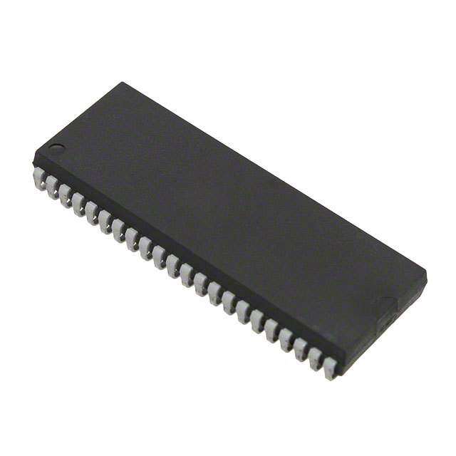
| 描述 | AHC HIGH PIN COUNT 16TSSOP |
| 产品分类 | |
| 品牌 | Diodes Incorporated |
| 数据手册 | |
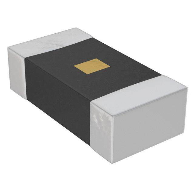
| 产品图片 |
|
| 产品型号 | 74AHCT594T16-13 |
| rohs | 无铅 / 符合限制有害物质指令(RoHS)规范要求 |
| RoHS指令信息 | http://diodes.com/download/4349 |
| 产品系列 | 74AHCT |
| 供应商器件封装 | 16-TSSOP |
| 元件数 | 1 |
| 其它名称 | 74AHCT594T16-13DICT |
| 功能 | 串行至并行,串行 |
| 包装 | 剪切带 (CT) |
| 安装类型 | 表面贴装 |
| 封装/外壳 | 16-TSSOP(0.173",4.40mm 宽) |
| 工作温度 | -40°C ~ 125°C |
| 标准包装 | 1 |
| 每元件位数 | 8 |
| 特色产品 | http://www.digikey.com/product-highlights/cn/zh/diodes-shift-registers-decoders/3896 |
| 电压-电源 | 4.5 V ~ 5.5 V |
| 输出类型 | 推挽式 |
| 逻辑类型 | 移位寄存器 |


PDF Datasheet 数据手册内容提取
74AHCT594 8-BIT SHIFT REGISTER WITH 8-BIT OUTPUT REGISTER Description Pin Assignments The 74AHCT594 is an advanced high speed CMOS device that is designed to be pin compatable with 74LS low power Schottky types. (Top View) An eight bit shift register accepts data from the serial input (DS) on Q1 1 16 Vcc each positive transition of the shift register clock (SHCP). When Q2 2 15 Q0 asserted low the shift register reset function (SHR) sets all shift register values to zero and is independent of all clocks. Also when Q3 3 14 DS asserted low, the storage register reset function (STR) sets all shift register values to zero and is independent of all clocks. Q4 4 13 STR Q5 5 12 STCP Data from the input serial shift register is placed in the output register with a rising pulse on the storages resister clock (STCP). The Q6 6 11 SHCP storage resister includes output Q7S which is used for cascading information between devices. As the information moves into the Q7 7 10 SHR storage register, it is asserted on the push-pull outputs Q0-Q7. GND 8 9 Q7S All registers capture data on rising edge and change output on the SO-16 /TSSOP-16 falling edge. If both clocks are connected together, the input shift register is always one clock cycle ahead of the output register. Features Applications Wide Supply Voltage Range from 4.5V to 5.5V General Purpose Logic Sinks or sources 8mA at VCC = 4.5V Serial to Parallel Data conversion CMOS low power consumption Capture and hold data for extended periods of time. Schmitt Trigger Action at All Inputs Allow simple serial bit streams from a microcontroller to control as Inputs accept up to 6.0V many peripheral lines as needed. ESD Protection Tested per JESD 22 Wide array of products such as: Exceeds 200-V Machine Model (A115-A) Computer Peripherals Exceeds 2000-V Human Body Model (A114-A) Appliances Exceeds 1000-V Charged Device Model (C101C) Industrial control Latch-Up Exceeds 250mA per JESD 78, Class II Totally Lead-Free & Fully RoHS Compliant (Notes 1 & 2) Halogen and Antimony Free. “Green” Device (Note 3) Notes: 1. No purposely added lead. Fully EU Directive 2002/95/EC (RoHS) & 2011/65/EU (RoHS 2) compliant. 2. See http://www.diodes.com/quality/lead_free.html for more information about Diodes Incorporated’s definitions of Halogen- and Antimony-free, "Green" and Lead-free. 3. Halogen- and Antimony-free "Green” products are defined as those which contain <900ppm bromine, <900ppm chlorine (<1500ppm total Br + Cl) and <1000ppm antimony compounds. Click here for ordering information, located at the end of datasheet 74AHCT594 1 of 10 June 2013 Document number: DS35485 Rev. 2 - 2 www.diodes.com © Diodes Incorporated
74AHCT594 Pin Descriptions Functional Diagram Pin Number Pin Name Description 1 Q1 Parallel Data Output 1 2 Q2 Parallel Data Output 2 3 Q3 Parallel Data Output 3 4 Q4 Parallel Data Output 4 5 Q5 Parallel Data Output 5 6 Q6 Parallel Data Output 6 7 Q7 Parallel Data Output 7 8 GND Ground 9 Q7S Serial Data Output 10 SHR Shift Register Reset active low 11 SHCP Shift Register Clock Input 12 STCP Storage Register Clock Input 13 STR Storage Register Reset active low 14 DS Serial Data input 15 Q0 Parallel Data Output 0 16 Vcc Supply Voltage Logic Diagram STAGE 0 STAGES 1 TO 6 STAGE 7 DS D Q D Q D Q FF0 FF7 CP CP R R SHCP SHR D Q D Q LATCH LATCH CP CP R R STCP STR Q0 Q1 Q2 Q3 Q4 Q5 Q6 Q7 74AHCT594 2 of 10 June 2013 Document number: DS35485 Rev. 2 - 2 www.diodes.com © Diodes Incorporated
74AHCT594 Functional Description and Timing Diagram Control Input Output Function SHR STR SHCP STCP DS Q7S Qn L X X X X L NC Clear Shift Register X L X X X NC L Clear Storage Register H X L H or L Q6S NC Loads DS into shift register stage 0. All QS shifted H H X X NC Qs Contents of shift register moved to starge register all QS -> QN H H H or L Q6S QnS Shift Register one pulse count ahead of storage register. H=HIGH voltage state L=LOW voltage state =LOW to HIGH transition X= don’t care – high or low (not floating) NC= No change Absolute Maximum Ratings (Note 4) (@TA = +25°C, unless otherwise specified.) Symbol Parameter Rating Unit ESD HBM Human Body Model ESD Protection 2 KV ESD CDM Charged Device Model ESD Protection 1 KV ESD MM Machine Model ESD Protection 200 V VCC Supply Voltage Range -0.5 to +7.0 V VI Input Voltage Range -0.5 to +7.0 V Vo Voltage applied to output in high or low state -0.3 to VCC +0.5 V IIK Input Clamp Current VI< -0.5V -20 mA IOK Output Clamp Current VO<-0.5V -20 mA IOK Output Clamp Current VO> VCC +0.5V 20 mA IO Continuous output current ±25 mA ICC Continuous current through Vcc 75 mA IGND Continuous current through GND -75 mA TJ Operating Junction Temperature -40 to +150 °C TSTG Storage Temperature -65 to +150 °C PTOT Total Power Dissipation 500 mW Notes: 4. Stresses beyond the absolute maximum may result in immediate failure or reduced reliability. These are stress values and device operation should be within recommend values. 74AHCT594 3 of 10 June 2013 Document number: DS35485 Rev. 2 - 2 www.diodes.com © Diodes Incorporated
74AHCT594 Recommended Operating Conditions (Note 5) (@TA = +25°C, unless otherwise specified.) Symbol Parameter Conditions Min Max Unit VCC Supply Voltage 4.5 5.5 V VI Input Voltage 0 5.5 V VO Output Voltage Active Mode 0 VCC V t/V Input transition Rise or Fall Rate VCC = 4.5V to 5.5V 20 ns/V TA Operating Free-Air Temperature -40 +125 °C Note: 5. Unused inputs should be held at V or Ground. CC Electrical Characteristics (@TA = +25°C, unless otherwise specified.) Symbol Parameter Test Conditions VCC TA = +25°C TA = -40°C to +85°C TA = -40°C to +125°C Unit Min Typ Max Min Max Min Max High-level Input VIH Voltage 4.5V to 5.5V 2.0 2.0 2.0 V Low-level input VIL voltage 4.5V to 5.5V 0.8 0.8 0.8 V High Level IOH = -50μA 4.5V 4.4 4.5 4.4 4.4 VOH Output Voltage IOH = -8mA 4.5V 3.94 3.80 3.70 V Low-level IOL = 50μA 4.5V 0 0.1 0.1 0.1 VOL Output Voltage IOL = 8mA 4.5V 0.36 0.44 0.55 V II Input Current VI = GND or 5.5V 0V to 5.5V 0.1 ±0.1 ± 1 ± 2 μA ICC Supply Current VIOI == 0 G ND or VCC 5.5V 4.0 40 80 μA Additional ∆ICC Supply Current VI = VCC -2.1V 4.5V to 5.5V 1.35 1.5 1.5 mA per Input IO = 0 Input Ci Capacitance Vi = VCC or GND 5.5V 3.5 10 10 10 pF 74AHCT594 4 of 10 June 2013 Document number: DS35485 Rev. 2 - 2 www.diodes.com © Diodes Incorporated
74AHCT594 Switching Characteristics PSayrmambeotle /r Pins Test Conditions VCC Min TA =T +yp25 °C Max -M40in°C to +8M5a°xC -4M0i°nC to +1M25a°xC Unit fMAX SHCP or Maximum STCP Figure 2 CL = 15pF 4.5V to 5.0V 90 160 80 70 MHz Frequency SHCP HIGH or LOW Figure 2 CL = 50pF 4.5V to 5.0V 5.5 6.0 6.5 PulsetW W idth HIGHST oCr PL OW Figure 2 CL = 50pF 4.5V to 5.0V 5.5 6.0 6.5 ns SHR and STR HIGH or LOW Figure 2 CL = 50pF 4.5V to 5.0V 5.2 5.5 6.0 DS to SHCP Figure 2 CL = 50pF 4.5V to 5.0V 3.0 3.0 3.5 tSU SHR to STCP Figure 2 CL = 50pF 4.5V to 5.0V 5.0 5.0 5.5 ns Set-up Time SHCP to STCP Figure 2 CL = 50pF 4.5V to 5.0V 5.0 5.0 5.5 Holdt HT ime DS to SHCP Figure 2 CL = 50pF 4.5V to 5.0V 5 2.0 2.0 2.5 ns SHR to SHCP RecovtReEryC Time and STR to Figure 2 CL = 50pF 4.5V to 5.0V 10 2.9 3.3 3.8 ns STCP Figure 2 CL = 15pF 4.5V to 5.0V 4.1 6.7 1.8 7.6 1.8 8.3 SHCP toQ7S tPLH Figure 2 CL = 50pF 4.5V to 5.0V 5.4 8.8 2.4 10.1 2.4 11.0 Propagation ns Delay STCP to Qn Figure 2 CL = 15pF 4.5V to 5.0V 3.7 6.1 1.9 6.9 1.9 7.2 Figure 2 CL = 50pF 4.5V to 5.0V 5.2 8.5 2.6 9.7 2.6 10.5 Figure 2 CL = 15pF 4.5V to 5.0V 4.1 6.7 1.8 7.6 1.8 8.3 SHCP to Q7S Figure 2 CL = 50pF 4.5V to 5.0V 5.4 8.8 2.4 10.1 2.4 11.0 ns Figure 2 CL = 15pF 4.5V to 5.0V 3.7 6.1 1.9 6.9 1.9 7.2 STCP to Qn tPHl Figure 2 CL = 50pF 4.5V to 5.0V 5.2 8.5 2.6 9.7 2.6 10.5 Propagation Delay SHR to Q7S Figure 2 CL = 15pF 4.5V to 5.0V 4.3 7.0 2.4 8.0 2.4 8.7 ns Figure 2 CL = 50pF 4.5V to 5.0V 5.4 8.8 2.7 10.1 2.7 11.0 Figure 2 CL = 15pF 4.5V to 5.0V 4.5 7.4 2.3 8.4 2.3 9.2 STR to Qn ns Figure 2 CL = 50pF 4.5V to 5.0V 5.7 9.4 3.1 10.7 3.1 11.7 Operating Characteristics (@TA = +25°C, unless otherwise specified.) Parameter Test VCC = 5V Unit Conditions Typ Power dissipation f = 1 MHz all outputs switching-no load Cpd capacitance VI = GND TO VCC -1.5V 51 pF 74AHCT594 5 of 10 June 2013 Document number: DS35485 Rev. 2 - 2 www.diodes.com © Diodes Incorporated
74AHCT594 Parameter Measurement Information Inputs VCC VM VI tr/tf 4.5V VCC 6ns VCC/2 5.0V VCC 6ns VCC/2 Voltage Waveform Voltage Waveform Pulse Duration and Recovery Time Set-up and Hold Times Voltage Waveform Propagation Delay Times Inverting and Non Inverting Outputs Notes: A. Includes test lead and test apparatus capacitance. B. All pulses are supplied at pulse repetition rate ≤ 10 MHz. C. Inputs are measured separately one transition per measurement. D. tPLH and tPHL are the same as tPD. Figure 2 Load Circuit and Voltage Waveforms 74AHCT594 6 of 10 June 2013 Document number: DS35485 Rev. 2 - 2 www.diodes.com © Diodes Incorporated
74AHCT594 Ordering Information 7” Tape and Reel (Note 6) Device Package Code Packaging Quantity Part Number Suffix 74AHCT594S16-13 S16 SO-16 2500/Tape & Reel -13 74AHCT594T16-13 T16 TSSOP-16 2500/Tape & Reel -13 Note: 6. The taping orientation is located on our website at http://www.diodes.com/datasheets/ap02007.pdf Marking Information (1) SO-16, TSSOP16 Part Number Package 74AHCT594S16 SO-16 74AHCT594T16 TSSOP-16 74AHCT594 7 of 10 June 2013 Document number: DS35485 Rev. 2 - 2 www.diodes.com © Diodes Incorporated
74AHCT594 Package Outline Dimensions (All dimensions in mm.) Please see AP02002 at http://www.diodes.com/datasheets/ap02002.pdf for latest version. Package Type: SO-16 SO-16 Dim Min Max E H Gauge Plane A 1.40 1.75 A1 0.10 0.25 L A2 1.30 1.50 B 0.33 0.51 Detail ‘A’ C 0.19 0.25 D 9.80 10.00 E 3.80 4.00 D A e 1.27 Typ A2 H 5.80 6.20 L 0.38 1.27 Θ 0 8 B e A1 C All Dimensions in mm Detail ‘A’ Package Type: TSSOP-16 TSSOP-16 Dim Min Max Typ A - 1.08 - A1 0.05 0.15 - E/2 A2 0.80 0.93 - SEE DETAIL 'A' b 0.19 0.30 - E E1 c 0.09 0.20 - Y D 4.90 5.10 - E 6.40 BSC E1 4.30 4.50 - X e 0.65 BSC PIN 1 L 0.45 0.75 - L1 1.00 REF e b x) L2 0.25 BSC Ø0.760Depth0.050±0.02 R 0.09 - - R1 0.09 - - A2 D R1 X - - 1.350 L2 R GAUGE Y - - 1.050 A C PLANE Θ 0° 8° - Θ1 5° 15° - SEATING PLANE L Θ2 0° - - All Dimensions in mm A1 L1 DETAIL 'A' 74AHCT594 8 of 10 June 2013 Document number: DS35485 Rev. 2 - 2 www.diodes.com © Diodes Incorporated
74AHCT594 Suggested Pad Layout Please see AP02001 at http://www.diodes.com/datasheets/ap02001.pdf for the latest version. Package Type: SO-16 X1 Dimensions Value (in mm) Y1 C 1.270 X 0.670 X1 9.560 Y 1.450 Y Y1 6.400 Pin 1 X C Package Type: TSSOP-16 X1 Dimensions Value (in mm) C 0.650 X 0.350 Y1 X1 4.900 Y (16x) Y 1.400 Y1 6.800 1 X (16x) C 74AHCT594 9 of 10 June 2013 Document number: DS35485 Rev. 2 - 2 www.diodes.com © Diodes Incorporated
74AHCT594 IMPORTANT NOTICE DIODES INCORPORATED MAKES NO WARRANTY OF ANY KIND, EXPRESS OR IMPLIED, WITH REGARDS TO THIS DOCUMENT, INCLUDING, BUT NOT LIMITED TO, THE IMPLIED WARRANTIES OF MERCHANTABILITY AND FITNESS FOR A PARTICULAR PURPOSE (AND THEIR EQUIVALENTS UNDER THE LAWS OF ANY JURISDICTION). Diodes Incorporated and its subsidiaries reserve the right to make modifications, enhancements, improvements, corrections or other changes without further notice to this document and any product described herein. Diodes Incorporated does not assume any liability arising out of the application or use of this document or any product described herein; neither does Diodes Incorporated convey any license under its patent or trademark rights, nor the rights of others. Any Customer or user of this document or products described herein in such applications shall assume all risks of such use and will agree to hold Diodes Incorporated and all the companies whose products are represented on Diodes Incorporated website, harmless against all damages. Diodes Incorporated does not warrant or accept any liability whatsoever in respect of any products purchased through unauthorized sales channel. Should Customers purchase or use Diodes Incorporated products for any unintended or unauthorized application, Customers shall indemnify and hold Diodes Incorporated and its representatives harmless against all claims, damages, expenses, and attorney fees arising out of, directly or indirectly, any claim of personal injury or death associated with such unintended or unauthorized application. Products described herein may be covered by one or more United States, international or foreign patents pending. Product names and markings noted herein may also be covered by one or more United States, international or foreign trademarks. This document is written in English but may be translated into multiple languages for reference. Only the English version of this document is the final and determinative format released by Diodes Incorporated. LIFE SUPPORT Diodes Incorporated products are specifically not authorized for use as critical components in life support devices or systems without the express written approval of the Chief Executive Officer of Diodes Incorporated. As used herein: A. Life support devices or systems are devices or systems which: 1. are intended to implant into the body, or 2. support or sustain life and whose failure to perform when properly used in accordance with instructions for use provided in the labeling can be reasonably expected to result in significant injury to the user. B. A critical component is any component in a life support device or system whose failure to perform can be reasonably expected to cause the failure of the life support device or to affect its safety or effectiveness. Customers represent that they have all necessary expertise in the safety and regulatory ramifications of their life support devices or systems, and acknowledge and agree that they are solely responsible for all legal, regulatory and safety-related requirements concerning their products and any use of Diodes Incorporated products in such safety-critical, life support devices or systems, notwithstanding any devices- or systems-related information or support that may be provided by Diodes Incorporated. Further, Customers must fully indemnify Diodes Incorporated and its representatives against any damages arising out of the use of Diodes Incorporated products in such safety-critical, life support devices or systems. Copyright © 2013, Diodes Incorporated www.diodes.com 74AHCT594 10 of 10 June 2013 Document number: DS35485 Rev. 2 - 2 www.diodes.com © Diodes Incorporated