ICGOO在线商城 > 隔离器 > 光隔离器 - 晶体管,光电输出 > 6N136SM
 Datasheet下载
- 型号: 6N136SM
- 制造商: Fairchild Semiconductor
- 库位|库存: xxxx|xxxx
- 要求:
| 数量阶梯 | 香港交货 | 国内含税 |
| +xxxx | $xxxx | ¥xxxx |
查看当月历史价格
查看今年历史价格
6N136SM产品简介:
ICGOO电子元器件商城为您提供6N136SM由Fairchild Semiconductor设计生产,在icgoo商城现货销售,并且可以通过原厂、代理商等渠道进行代购。 6N136SM价格参考¥4.39-¥13.56。Fairchild Semiconductor6N136SM封装/规格:光隔离器 - 晶体管,光电输出, 光隔离器 有基极的晶体管 输出 5000Vrms 1 通道 8-SMD。您可以下载6N136SM参考资料、Datasheet数据手册功能说明书,资料中有6N136SM 详细功能的应用电路图电压和使用方法及教程。
ON Semiconductor的6N136SM是一款光隔离器(光电耦合器),属于光隔离器 - 晶体管、光电输出类别。其主要功能是通过光信号实现输入与输出之间的电气隔离,同时提供高速信号传输能力。以下是该型号的一些典型应用场景:

 1. 工业自动化控制
   - 在工业控制系统中,6N136SM可用于隔离传感器信号与控制器之间的连接,防止噪声干扰或高电压对敏感电路的影响。
   - 例如,在PLC(可编程逻辑控制器)中,用于数字输入/输出接口的信号隔离。

 2. 通信设备
   - 用于隔离通信接口(如RS-232、RS-485等)中的数据信号,确保信号完整性并保护系统免受浪涌或地电位差的影响。
   - 在光纤通信系统中,作为电信号与光信号转换后的隔离元件。

 3. 医疗设备
   - 在医疗电子设备中(如心电图仪、血压监测仪等),6N136SM可用于隔离患者接触部分与设备主控板之间的信号,确保患者和设备的安全。

 4. 电源管理
   - 在开关电源或DC-DC转换器中,用于反馈信号的隔离,避免高压侧对低压控制电路的干扰。
   - 适用于需要高可靠性和低噪声的电源设计。

 5. 汽车电子
   - 在汽车电子控制系统中,用于隔离传感器信号(如氧传感器、轮速传感器等)与ECU(电子控制单元)之间的连接。
   - 提供抗电磁干扰能力,确保信号的稳定传输。

 6. 家用电器
   - 在智能家电中,用于隔离用户界面与主控板之间的信号,提高系统的安全性和可靠性。
   - 例如,在洗衣机、空调等设备中,用于电机驱动信号的隔离。

 7. 音频设备
   - 在音频设备中,用于隔离音频信号路径,减少噪声干扰,提升音质表现。

 特性总结
6N136SM具有以下关键特性:
- 高速响应(典型传播延迟为5μs)。
- 高共模抑制能力(>25kV/μs)。
- 输入LED与输出晶体管之间的良好隔离性能(额定隔离电压通常为2500Vrms)。
- 工作温度范围广(-40°C至+105°C),适合多种环境条件。

这些特性使其成为需要高可靠性和电气隔离的应用的理想选择。
| 参数 | 数值 |
| 产品目录 | |
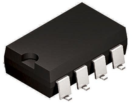
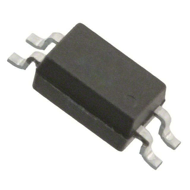
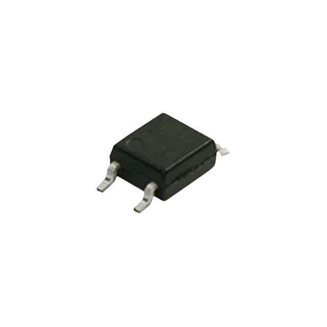
| 描述 | OPTOISO 5KV TRANS W/BASE 8SMD高速光耦合器 8P-DIP SM HI SPEED TRANSISTOR OPTOCOUP |
| 产品分类 | |
| 品牌 | Fairchild Semiconductor |
| 产品手册 | |
| 产品图片 |
|
| rohs | 符合RoHS无铅 / 符合限制有害物质指令(RoHS)规范要求 |
| 产品系列 | 光耦合器/光电耦合器,高速光耦合器,Fairchild Semiconductor 6N136SM- |
| 数据手册 | |
| 产品型号 | 6N136SM |
| Vce饱和值(最大值) | - |
| 上升/下降时间(典型值) | - |
| 上升时间 | 0.8 us |
| 下降时间 | 0.8 us |
| 产品种类 | 高速光耦合器 |
| 供应商器件封装 | 8-SMD |
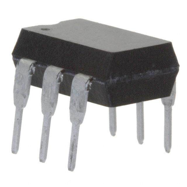
| 包装 | 管件 |
| 单位重量 | 720 mg |
| 商标 | Fairchild Semiconductor |
| 安装类型 | 表面贴装 |
| 封装 | Bulk |
| 封装/外壳 | 8-SMD,鸥翼型 |
| 封装/箱体 | SMD-8 |
| 工作温度 | -40°C ~ 100°C |
| 工厂包装数量 | 1000 |
| 打开/关闭时间(典型值) | 800ns, 800ns (最小值) |
| 数据速率 | 1 MBd |
| 最大功率耗散 | 100 mW |
| 最大反向二极管电压 | 5 V |
| 最大工作温度 | + 100 C |
| 最大正向二极管电压 | 1.7 V |
| 最小工作温度 | - 55 C |
| 标准包装 | 1,000 |
| 正向电流 | 25 mA |
| 每芯片的通道数量 | 1 Channel |
| 电压-正向(Vf)(典型值) | 1.45V |
| 电压-输出(最大值) | 20V |
| 电压-隔离 | 5000Vrms |
| 电流-DC正向(If) | 25mA |
| 电流-输出/通道 | 8mA |
| 电流传输比(最大值) | 50% @ 16mA |
| 电流传输比(最小值) | 19% @ 16mA |
| 电流传递比 | 38 % |
| 系列 | 6N136M |
| 绝缘电压 | 5000 Vrms |
| 输入类型 | DC |
| 输出类型 | 有基极的晶体管 |
| 输出设备 | Phototransistor |
| 通道数 | 1 |


.jpg)


- 商务部:美国ITC正式对集成电路等产品启动337调查
- 曝三星4nm工艺存在良率问题 高通将骁龙8 Gen1或转产台积电
- 太阳诱电将投资9.5亿元在常州建新厂生产MLCC 预计2023年完工
- 英特尔发布欧洲新工厂建设计划 深化IDM 2.0 战略
- 台积电先进制程称霸业界 有大客户加持明年业绩稳了
- 达到5530亿美元!SIA预计今年全球半导体销售额将创下新高
- 英特尔拟将自动驾驶子公司Mobileye上市 估值或超500亿美元
- 三星加码芯片和SET,合并消费电子和移动部门,撤换高东真等 CEO
- 三星电子宣布重大人事变动 还合并消费电子和移动部门
- 海关总署:前11个月进口集成电路产品价值2.52万亿元 增长14.8%
.jpg)

PDF Datasheet 数据手册内容提取
Is Now Part of To learn more about ON Semiconductor, please visit our website at www.onsemi.com Please note: As part of the Fairchild Semiconductor integration, some of the Fairchild orderable part numbers will need to change in order to meet ON Semiconductor’s system requirements. Since the ON Semiconductor product management systems do not have the ability to manage part nomenclature that utilizes an underscore (_), the underscore (_) in the Fairchild part numbers will be changed to a dash (-). This document may contain device numbers with an underscore (_). Please check the ON Semiconductor website to verify the updated device numbers. The most current and up-to-date ordering information can be found at www.onsemi.com. Please email any questions regarding the system integration to Fairchild_questions@onsemi.com. ON Semiconductor and the ON Semiconductor logo are trademarks of Semiconductor Components Industries, LLC dba ON Semiconductor or its subsidiaries in the United States and/or other countries. ON Semiconductor owns the rights to a number of patents, trademarks, copyrights, trade secrets, and other intellectual property. A listing of ON Semiconductor’s product/patent coverage may be accessed at www.onsemi.com/site/pdf/Patent-Marking.pdf. ON Semiconductor reserves the right to make changes without further notice to any products herein. ON Semiconductor makes no warranty, representation or guarantee regarding the suitability of its products for any particular purpose, nor does ON Semiconductor assume any liability arising out of the application or use of any product or circuit, and specifically disclaims any and all liability, including without limitation special, consequential or incidental damages. Buyer is responsible for its products and applications using ON Semiconductor products, including compliance with all laws, regulations and safety requirements or standards, regardless of any support or applications information provided by ON Semiconductor. “Typical” parameters which may be provided in ON Semiconductor data sheets and/or specifications can and do vary in different applications and actual performance may vary over time. All operating parameters, including “Typicals” must be validated for each customer application by customer’s technical experts. ON Semiconductor does not convey any license under its patent rights nor the rights of others. ON Semiconductor products are not designed, intended, or authorized for use as a critical component in life support systems or any FDA Class 3 medical devices or medical devices with a same or similar classification in a foreign jurisdiction or any devices intended for implantation in the human body. Should Buyer purchase or use ON Semiconductor products for any such unintended or unauthorized application, Buyer shall indemnify and hold ON Semiconductor and its officers, employees, subsidiaries, affiliates, and distributors harmless against all claims, costs, damages, and expenses, and reasonable attorney fees arising out of, directly or indirectly, any claim of personal injury or death associated with such unintended or unauthorized use, even if such claim alleges that ON Semiconductor was negligent regarding the design or manufacture of the part. ON Semiconductor is an Equal Opportunity/Affirmative Action Employer. This literature is subject to all applicable copyright laws and is not for resale in any manner.
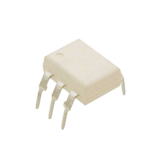
DS uin ag l -l January 2016 Ce h-C ah n a nn en Single-Channel: 6N135M, 6N136M, HCPL4503M l :e Hl: Dual-Channel: HCPL2530M, HCPL2531M C 6 PN 8-Pin DIP High Speed Transistor Optocouplers L1 23 55 3M 0, Features Description M 6 ,N • High Speed – 1 MBit/s The 6N135M, 6N136M, HCPL4503M, HCPL2530M, and H1 C3 • Dual-Channel: HCPL2530M, HCPL2531M HCPL2531M optocouplers consist of an AlGaAs LED P6 M optically coupled to a high speed photodetector transis- L • CTR Guaranteed 0°C to 70°C tor for each channel. 25, H • No Base Connection for Improved Noise Immunity 3C (HCPL4503M) A separate connection for the bias of the photodiode 1P M improves the speed by several orders of magnitude over L •• SSuafpeetyri oarn CdM RRe gouf la15to,r0y0 A0 pVp/μrosv Malsinimum (HCPL4503M) conventional phototransistor optocouplers by reducing —45 the base-collector capacitance of the input transistor. 8 0 – UL1577, 5,000 VACRMS for 1 Minute -P3M – DIN EN/IEC60747-5-5 The HCPL4503M has no internal connection to the pho- in totransistor base for improved noise immunity. An inter- D nal noise shield provides superior common mode I P rejection of up to 50,000 V/μs. Applications H Related Resources ig • Line Receivers h • Pulse Transformer Replacement • www.fairchildsemi.com/products/optoelectronics/ S p • Output Interface to CMOS-LSTTL-TTL • www.fairchildsemi.com/pf/HC/HCPL0500.html e e • Wide-Bandwidth Analog Coupling • www.fairchildsemi.com/pf/FO/FODM452.html d • www.fairchildsemi.com/pf/FO/FOD050L.html T r a n Schematics Package Outlines s i s t o r O p N/C 1 8 VCC + 1 8 VCC 8 8 to c V 1 1 o F1 u _ p + 2 7 V 2 7 V l B 01 e r V s F 8 _ 3 6 V _ 3 6 V 8 O 02 1 1 V F2 Figure 2. Package Outlines N/C 4 5 GND + 4 5 GND 6N135M, 6N136M, HCPL4503M HCPL2530M, HCPL2531M Pin 7 is not connected in the HCPL4503M Figure 1. Schematics ©2008 Fairchild Semiconductor Corporation www.fairchildsemi.com 6N13XM, HCPLXXXXM Rev. 1.7
DS uin Safety and Insulation Ratings ag l -l Ce As per DIN EN/IEC 60747-5-5, this optocoupler is suitable for “safe electrical insulation” only within the safety limit h-C data. Compliance with the safety ratings shall be ensured by means of protective circuits. ah n a Parameter Characteristics nn en l < 150 VRMS I–IV : Hel: Installation Classifications per DIN VDE < 300 VRMS I–IV C 6 PN 0110/1.89 Table 1, For Rated Mains Voltage < 450 VRMS I–III L1 23 < 600 V I–III 55 RMS 3M Climatic Classification 40/100/21 0, M 6 Pollution Degree (DIN VDE 0110/1.89) 2 ,N H1 Comparative Tracking Index 175 C3 P6 M L 2, 5H Symbol Parameter Value Unit 3C 1P M Input-to-Output Test Voltage, Method A, V x 1.6 = V , L Type and Sample Test with tm = 10 s, PartIiOaRl DMischarge <P R5 pC 1,335 Vpeak —45 VPR 8 0 I1n0p0u%t-t oP-rOoduutpcutito Tne Tset sVt owltiathg et, M =e 1th so, dP Bar, tViaIlO DRiMs cxh 1a.r8g7e5 < = 5 V pPCR, 1,669 Vpeak -P3M m in VIORM Maximum Working Insulation Voltage 890 Vpeak D I V Highest Allowable Over-Voltage 6,000 V P IOTM peak External Creepage ≥ 8.0 mm H i g External Clearance ≥ 7.4 mm h External Clearance (for Option TV, 0.4" Lead Spacing) ≥ 10.16 mm S p DTI Distance Through Insulation (Insulation Thickness) ≥ 0.5 mm ee d TS Case Temperature(1) 150 °C T IS,INPUT Input Current(1) 200 mA ra n P Output Power (Duty Factor ≤ 2.7%)(1) 300 mW s S,OUTPUT i RIO Insulation Resistance at TS, VIO = 500 V(1) > 109 Ω sto r Note: O 1. Safety limit value - maximum values allowed in the event of a failure. p t o c o u p l e r s ©2008 Fairchild Semiconductor Corporation www.fairchildsemi.com 6N13XM, HCPLXXXXM Rev. 1.7 2
DS uin Absolute Maximum Ratings ag l -l Stresses exceeding the absolute maximum ratings may damage the device. The device may not function or be Ce operable above the recommended operating conditions and stressing the parts to these levels is not recommended. h-C In addition, extended exposure to stresses above the recommended operating conditions may affect device reliability. ah n The absolute maximum ratings are stress ratings only. TA = 25°C unless otherwise specified. nan en Symbol Parameter Test Conditions Value Unit l:e Hl: TSTG Storage Temperature -40 to +125 °C C 6 PN TOPR Operating Temperature -40 to +100 °C L1 23 TJ Junction Temperature -40 to +125 °C 55 3M TSOL Lead Solder Temperature 260 for 10 sec °C 0M, 6 EMITTER ,N H1 DC/Average Forward Input Current C3 IF (avg) Each Channel(2) 25 mA PL6M Peak Forward Input Current 50% Duty Cycle, 25, H I (pk) 50 mA F Each Channel(3) 1 ms P.W. 3C 1P M IF (trans) Peak Transient Input Current Each Channel ≤ 1 μs P.W., 300 pps 1.0 A —L4 5 V Reverse Input Voltage Each Channel 5 V R 8 0 PD Input Power Dissipation Each Channel(4) 45 mW -P3M DETECTOR in D IO (avg) Average Output Current Each Channel 8 mA IP IO (pk) Peak Output Current Each Channel 16 mA H i V Emitter-Base Reverse Voltage 6N135M and 6N136M 5 V g EBR h VCC Supply Voltage -0.5 to 30 V S p VO Output Voltage -0.5 to 20 V e e I Base Current 6N135M and 6N136M 5 mA d B PD Output Power Dissipation Each Channel(5) 100 mW Tr a n Notes: s 2. Derate linearly above 70°C free-air temperature at a rate of 0.8 mA/°C. is 3. Derate linearly above 70°C free-air temperature at a rate of 1.6 mA/°C. to 4. Derate linearly above 70°C free-air temperature at a rate of 0.9 mW/°C. r O 5. Derate linearly above 70°C free-air temperature at a rate of 2.0 mW/°C. p t o c o u Recommended Operating Conditions p l The Recommended Operating Conditions table defines the conditions for actual device operation. Recommended e r operating conditions are specified to ensure optimal performance to the datasheet specifications. Fairchild does not s recommend exceeding them or designing to absolute maximum ratings. Symbol Parameter Min. Max. Unit V Supply Voltage 4.5 20.0 V CC T Ambient Operating Temperature 0 70 °C A I Input Current, Low Level 0 250 μA FL I Input Current, High Level(6) 6.3 20.0 mA FH Note: 6. 6.3 mA is a guard banded value which allows for at least 20% CTR degradation. Initial input current threshold value is 5.0 mA or less. ©2008 Fairchild Semiconductor Corporation www.fairchildsemi.com 6N13XM, HCPLXXXXM Rev. 1.7 3
DS uin Electrical Characteristics ag l -l V = 5.0 V, T = 0°C to 70°C unless otherwise specified. Ce CC A h-C Individual Component Characteristics ah n a Symbol Parameter Device Test Conditions Min. Typ. Max. Unit nenn l :e EMITTER Hl: All I = 16 mA, T = 25°C 1.45 1.70 C 6 V Input Forward Voltage F A V PN F All I = 16 mA 1.80 L1 F 23 B Input Reverse All I = 10 µA 5 21 V 535M VR Breakdown Voltage R 0, M 6 ΔVF/ΔTA Toef mFoprewraatrudr eV oCltoaegfeficient All IF = 16 mA -1.7 mV/°C , HN1 C3 DETECTOR P6 M L I = 0 mA, V = V = 5.5 V, 2, All F O CC 0.0007 0.5 5H TA = 25°C 3C 1P I Logic High Output 6N135M, I = 0 mA, V = V = 15 V, µA ML OH Current 6N136M, F O CC 0.0019 1 —4 T = 25°C 5 HCPL4503M A 8 0 -3 All I = 0 mA, V = V = 15 V 50 PM F O CC in 6N135M, 6N136M, IF = 16 mA, VO = Open, 163 200 D ICCL LCougrrice nLtow Supply HCPL4503M VCC = 15 V µA IP H HCPL2530M, IF1 = IF2 = 16 mA, 400 ig HCPL2531M VO = Open, VCC = 15 V h 6N135M, S I = 0 mA, V = Open, p 6N136M, F O 0.0004 2 e ICCH LCougrrice nHtigh Supply HCPL4503M VCC = 15 V µA ed HCPL2530M, I = 0 mA, V = Open, T F O 4 r HCPL2531M V = 15 V a CC n s i s t o r O p t o c o u p l e r s ©2008 Fairchild Semiconductor Corporation www.fairchildsemi.com 6N13XM, HCPLXXXXM Rev. 1.7 4
DS uin Electrical Characteristics (continued) ag l -l T = 0°C to 70°C unless otherwise specified. Ce A h-C Transfer Characteristics ah n a Symbol Parameter Device Test Conditions Min. Typ. Max. Unit nenn l :e COUPLED Hl: 6N135M, C 6 7 38 50 % PN HCPL2530M L1 IF = 16 mA, VO = 0.4 V, 23 6N136M, V = 4.5 V, T = 25°C 55 CC A 3M HCPL4503M, 19 38 50 % 0, HCPL2531M M 6 CTR CRautriroe(n7)t Transfer 6N135M VOL = 0.4 V , HN1 5 % C3 HCPL2530M VOL = 0.5 V P6 I = 16 mA, M F L 6HNC1P3L64M50,3M VCC = 4.5 V VOL = 0.4 V 15 % 25, H 3C HCPL2531M V = 0.5 V 1P OL M L 6N135M I = 16 mA, I = 1.1 mA, 0.4 —4 F O 0.12 5 HCPL2530M VCC = 4.5 V, TA = 25°C 0.5 8 0 -3 PM 6N136M, HCPL4503M IF = 16 mA, IO = 3 mA, 0.20 0.4 in Logic LOW Output V = 4.5 V, T = 25°C D VOL Voltage HCPL2531M CC A 0.5 V IP 6N135M, IF = 16 mA, IO = 0.8 mA, 0.11 0.5 H HCPL2530M VCC = 4.5 V ig h HCPL4503M, IF = 16 mA, IO = 2.4 mA, 0.18 0.5 S HCPL2531M VCC = 4.5 V p e Note: e d 7. Current Transfer Ratio is defined as a ratio of output collector current, IO, to the forward LED input current, IF, times T 100%. r a n s i s t o r O p t o c o u p l e r s ©2008 Fairchild Semiconductor Corporation www.fairchildsemi.com 6N13XM, HCPLXXXXM Rev. 1.7 5
DS uin Electrical Characteristics (continued) ag l -l T = 0°C to 70°C unless otherwise specified. Ce A h-C Switching Characteristics ah n a Symbol Parameter Device Test Conditions Min. Typ. Max. Unit nenn l :e H6NC1P3L52M530M TIFA = = 1 265 m°CA, (R8)L ( F=i g4u.1re k Ω15,) 00..2253 1.5 µs HCl: 6 PN 6N136M, L1 T = 25°C, R = 1.9 kΩ, 0.25 23 HCPL4503M A L 0.8 µs 55 tPHL PTirmopea tgoa Ltioogni cD LeOlaWy HCPL2531M IF = 16 mA(9) (Figure 15) 0.28 30MM, 6 6N135M, RL = 4.1 kΩ, IF = 16 mA(8) 2.0 µs , N HCPL2530M (Figure 15) H1 C3 6N136M, P6 HCPL4503M, R(FLig =u r1e.9 1 k5Ω), IF = 16 mA(9) 1.0 µs L2M, HCPL2531M 5H 3C H6NC1P3L52M530M TIFA = = 1 265 m°CA, (R8)L ( F=i g4u.1re k Ω15,) 00..2495 1.5 µs 1M —PL4 5 6N136M, 8 0 HCPL4503M TA = 25°C, RL = 1.9 kΩ, 0.26 0.8 µs -P3M Propagation Delay HCPL2531M IF = 16 mA(9) (Figure 15) 0.18 in tPLH Time to Logic HIGH D 6N135M, RL = 4.1 kΩ, IF = 16 mA(8) 2.0 µs IP HCPL2530M (Figure 15) H 6N136M, i R = 1.9 kΩ, I = 16 mA(9) g HCPL4503M, L F 1.0 µs h (Figure 15) HCPL2531M S p I = 0 mA, V = 10 V , e 6HNC1P3L52M53,0M RFL = 4.1 kΩ,C TMA = 25°CP(-1P0) 10,000 ed (Figure 16) T r Common Mode I = 0 mA, V = 10 V , a 6N136M, F CM P-P n |CM | Transient Immunity at R = 1.9 kΩ, T = 25°C(10) 10,000 V/µs s H HCPL2531M L A i Logic High (Figure 16) s t o IF = 0 mA, VCM = 1,500 VP-P, r HCPL4503M R = 4.1 kΩ, T = 25°C(10) 15,000 50,000 O L A (Figure 16) p t o 6N135M, IRF = = 1 46. 1m kAΩ, ,V TCM = = 2 150°C V(P10-P), 10,000 co HCPL2530M L A u (Figure 16) p l e Common Mode I = 16 mA, V = 10 V , |CM | Transient Immunity at 6N136M, RF = 1.9 kΩ(10C)M P-P 10,000 V/µs rs L HCPL2531M L Logic Low (Figure 16) I = 0 mA, V = 1,500 V , F CM P-P HCPL4503M R = 4.1 kΩ, T = 25°C(10) 15,000 50,000 L A (Figure 16) Notes: 8. The 4.1 kΩ load represents 1 LSTTL unit load of 0.36 mA and 6.1 kΩ pull-up resistor. 9. The 1.9 kΩ load represents 1 TTL unit load of 1.6 mA and 5.6 kΩ pull-up resistor. 10.Common mode transient immunity in logic high level is the maximum tolerable (positive) dV /dt on the leading edge cm of the common mode pulse signal, V , to assure that the output will remain in a logic high state (i.e., V > 2.0 V). CM O Common mode transient immunity in logic low level is the maximum tolerable (negative) dV /dt on the trailing edge cm of the common mode pulse signal, V , to assure that the output will remain in a logic low state (i.e., V < 0.8 V). CM O ©2008 Fairchild Semiconductor Corporation www.fairchildsemi.com 6N13XM, HCPLXXXXM Rev. 1.7 6
DS uin Isolation Characteristics (T = 25°C unless otherwise specified.) ag A l -l Ce Symbol Parameter Device Test Conditions Min. Typ. Max. Unit h-C V Withstand Isolation All Rt =H 1 ≤ m 5i0n%ut,e I,I -O ≤ 10 µA 5,000 VAC annhan ISO Test Voltage f = 50 Hz(11)(13) RMS eln :e R Resistance All V = 500 V (11) 1011 Ω HCl: 6 I-O (Input to Output) I-O DC PN L1 CI-O C(Inappuatc titoa nOcuet put) All f = 1 MHz, VI-O = 0 VDC(11) 1 pF 2535 3M I Input-Input Insulation HCPL2530M, RH ≤ 45%, < 1 nA 0M, 6 I-I Leakage Current HCPL2531M VI-I = 500 VDC, t = 5 s(12) , N H1 RI-I Input-Input Resistance HHCCPPLL22553301MM, VI-I = 500 VDC(12) 1012 Ω CP36 M L CI-I Input-Input Capacitance HHCCPPLL22553301MM, f = 1 MHz(12) 0.2 pF 253, HC 1P M Notes: L 11.Device is considered a two terminal device: pins 1, 2, 3 and 4 are shorted together and pins 5, 6, 7 and 8 are shorted —45 together. 8 0 -3 12.Measured between pins 1 and 2 shorted together, and pins 3 and 4 shorted together. PM 13. 5000 V for 1 minute duration is equivalent to 6000 V for 1 second duration. in RMS RMS D I P H i g h S p e e d T r a n s i s t o r O p t o c o u p l e r s ©2008 Fairchild Semiconductor Corporation www.fairchildsemi.com 6N13XM, HCPLXXXXM Rev. 1.7 7
DS uin Typical Performance Curves ag l -l Ce For single-channel devices; 6N135M, 6N136M, and HCPL4503M. h-C ah n a )Am 61 = I( RTC / )I(RFF1111....6420 )Am 61 = T( RTC / )T(RAA 011...802 nel: HCPL253nnel: 6N135M TC )D 0.8 TC )D 0.6 0M, 6 EZILAMRO 00..64 NIFo =rm 1a6l imzeAd to: VVTAOC C == = 20 5.54° VC V EZILAMRO 00..24 NTAo r=m 2a5li°zCed to: IVVFCO =C = 1= 06 .4m4.V5AV , HCPN136M N 0.2 N L ( RT ( RT 25, H C 0.0 C 0.0 3C 0.1 1 10 100 -40 -20 0 20 40 60 80 100 120 1P IF - FORWARD CURRENT (mA) TA - TEMPERATURE (°C) ML Figure 3. Normalized CTR vs. Forward Current Figure 4. Normalized CTR vs. Temperature —45 8 0 -P3M 25 1000 in )Am( TN 20 TVAC C= =2 55° VC IF = 433050 mmmAAA )An( TNERRUC 100 IVVFCO =C = 0= 5 m.55.A 5V V DIP Hig ERRUC T 15 2250 mmAA TUPTUO 10 h Sp UPTU 10 15 mA HGIH eed O –I O 5 150 m mAA CIGOL 1 Tra – H n O s 0 I 0.1 i 0 2 4 6 8 10 12 14 16 18 20 -40 -20 0 20 40 60 80 100 120 s t VO – OUTPUT VOLTAGE (V) TA – TEMPERATURE (°C) o r Figure 5. Output Current vs. Output Voltage Figure 6. Logic High Output Current vs. Temperature O p t o 800 c )sn( YALED 567000000 FDVrCuetCqy u =Ce 5ync cVlye == 1100 %kHz RL = 4.1 kΩ (tPLH) )sn( YALED 1000 FDVrCuetCqy u =Ce 5ync cVlye == 1100 %kHz IF = 16 mA (tPLH) ouplers NOITAGAPO 340000 RL R=L 1 =.9 1 k.9Ω k (ΩtP (LtHP)HL) NOITAGAPO IFI F= 1=0 1 m0 Am (AtP (HtPLL)H) RP – P200 RL = 4.1 kΩ (tPHL) TPRP - IF = 16 mA (tPHL) t 100 0 100 -40 -20 0 20 40 60 80 100 120 1 10 TA – TEMPERATURE (°C) RL – LOAD RESISTANCE (kΩ) Figure 7. Propagation Delay vs. Temperature Figure 8. Propagation Delay vs. Load Resistance ©2008 Fairchild Semiconductor Corporation www.fairchildsemi.com 6N13XM, HCPLXXXXM Rev. 1.7 8
DS uin Typical Performance Curves (Continued) ag l -l Ce For dual-channel devices; HCPL2530M and HCPL2531M. h-C ah n a )Am 61 = I( RTC / )I(RTFF11110.....64208 ° )C52 = T( RTC / )T(RTAA 0011....6802 nel: HCPL253nnel: 6N135M C )D C )D 0M, 6 EZILAMRO 00..64 NIFo =rm 1a6l imzeAd to: VTVAOC C == = 20 5.54° VC V EZILAMRO 00..24 NTAo r=m 2a5li°zCed to: IVVFCO =C = 1= 06 .4 4m. 5VA V , HCPN136 N( RTC 00..20 N( RTC 0.0 L25M, H 0.1 1 10 100 -40 -20 0 20 40 60 80 100 120 3C IF - FORWARD CURRENT (mA) TA - TEMPERATURE (°C) 1MP L Figure 9. Normalized CTR vs. Forward Current Figure 10. Normalized CTR vs. Temperature —4 5 8 0 -3 PM 20 VTAC C= =2 55° VC )An( T1000 IVFC =C 0= m5.A5 V in D )A NE VO = 5.5 V IP m( T 15 IF = 40 mA RRU 100 H NERRUC 10 3350 mmAA C TUPTU 10 igh S TUPTUO –I O 5 221155050 m mmmmAAAAA O HGIH CIGOL – 1 peed Tra HO n 0 I 0.1 s 0 2 4 6 8 10 12 14 16 18 20 -40 -20 0 20 40 60 80 100 120 is VO – OUTPUT VOLTAGE (V) TA – TEMPERATURE (°C) to r Figure 11. Output Current vs. Output Voltage Figure 12. Logic High Output Current vs. Temperature O p t o 600 c Frequency = 10 kHz Frequency = 10 kHz o )sn( YALED N 540000 DVCutCy =C 5yc Vle = 10% RRLL == 41..19 kkΩΩ ((ttPPLHHL)) )sn( YALED N 1000 TDVACu tC=y =2C 55y°c CVle = 10% uplers OITAG 300 OITAG IF = 10 mA (tPHL) APORP – tP210000 RRLL == 41..19 kkΩΩ ((ttPPHLHL)) TPAPORP - IIFF == 1166 mmAA ((ttPPHLLH)) IF = 10 mA (tPLH) 0 100 -40 -20 0 20 40 60 80 100 120 1 10 TA – TEMPERATURE (°C) RL – LOAD RESISTANCE (kΩ) Figure 13. Propagation Delay vs. Temperature Figure 14. Propagation Delay vs. Load Resistance ©2008 Fairchild Semiconductor Corporation www.fairchildsemi.com 6N13XM, HCPLXXXXM Rev. 1.7 9
DS uin Test Circuits ag l -l Ce h-C I1tGPZ/r f0 u Oe =<% ln=s 51e e5Dn0r0as0.Ct Ωoμ.sr IF V+F- 321 SNhoiiesled 678 VVVOBCC RL +V5O V 1I/0f %<PGtZ 1rD u Oe0 =U ln=0s 5Te eμ5 YrnS0a sCtΩoYrCLEIF --V+F1 123 NShoiiesled 876 VVVC0012C RL C L = +1V55O VpF annel: HCPhannel: 6N I F MonitoRrm 4 5 GND 0.1 μF C L = 15 pF MONIIFTOR Rm +VF2 4 5 GND 0.1 μF L253135M 0, M 6 Test Circuit for HCPL2530M and HCPL2531M , N H1 Test Circuit for 6N135M, 6N136M, and HCPL4503M C3 P6 M L IF 2, 0 5H 3C 1P M VO 5 V —L4 5 1.5 V 1.5 V 8 0 VOL -P3M TPHL TPLH in D Figure 15. Switching Time Test Circuit I P H i g h IF Noise Noise S 1 Shield 8 VCC +5 V + 1 Shield 8 VCC +5 V pe + 2 7 VB RL IF V-F1 2 7 V01 RL VO ed T VFF B A VF- 3 6 GVOND 0.1 μFVO VFF BA +-VF2 3 6 GV0N2D 0.1 μF ransis 4 5 – 4 5 t o r + V-CM O VCM p Pulse Gen + - t o Pulse Gen c o Test Circuit for 6N135M, 6N136M, and HCPL4503M Test Circuit for HCPL2530M and HCPL2531M u p l e r s VC M 10 V 90% 90% 10% 10% 0 V tr tf VO 5 V Switch at A : I F = 0 mA VO VOL Switch at A : I F = 16 mA Figure 16. Common Mode Immunity Test Circuit ©2008 Fairchild Semiconductor Corporation www.fairchildsemi.com 6N13XM, HCPLXXXXM Rev. 1.7 10
DS uin Reflow Profile ag l -l Ce h-C ah n a TP MMaxaixmimumum R Ramamp-pd-ouwp nR Rataet e= =3 °6C°C/S/S nelnn 260 :e 240 tP HCl: 6 220 TL PN L1 200 Tsmax 23 ) 180 Preheat Area tL 535M C 0, e (° 116400 Tsmin M, 6N ur ts H1 t 120 C3 a P6 er 100 LM mp 80 25, H Te 60 31CP M 40 L —4 20 5 8 0 0 -3 PM 120 240 360 in Time 25°C to Peak D Time (seconds) IP H i g h S p e Profile Freature Pb-Free Assembly Profile e d Temperature Min. (Tsmin) 150°C T r Temperature Max. (Tsmax) 200°C a n Time (t ) from (Tsmin to Tsmax) 60 to 120 s s S i s Ramp-up Rate (tL to tP) 3°C/second maximum to Liquidous Temperature (TL) 217°C r O Time (t ) Maintained Above (T ) 60 to 150 s p L L t o Peak Body Package Temperature 260°C +0°C / –5°C c o Time (tP) within 5°C of 260°C 30 s u p Ramp-down Rate (TP to TL) 6°C/s maximum le r Time 25°C to Peak Temperature 8 minutes maximum s Figure 17. Relow Profile ©2008 Fairchild Semiconductor Corporation www.fairchildsemi.com 6N13XM, HCPLXXXXM Rev. 1.7 11
DS uin Ordering Information ag l -l Ce Part Number Package Packing Method h-C ah 6N135M DIP 8-Pin Tube (50 units per tube) n a nn 6N135SM SMT 8-Pin (Lead Bend) Tube (50 units per tube) en l :e 6N135SDM SMT 8-Pin (Lead Bend) Tape and Reel (1,000 units per reel) Hl: 6N135VM DIP 8-Pin, DIN EN/IEC 60747-5-5 Option Tube (50 units per tube) C 6 PN 6N135SVM SMT 8-Pin (Lead Bend), DIN EN/IEC 60747-5-5 Option Tube (50 units per tube) L1 23 6N135SDVM SMT 8-Pin (Lead Bend), DIN EN/IEC 60747-5-5 Option Tape and Reel (1,000 units per reel) 55 3M 6N135TVM DIP 8-Pin, 0.4” Lead Spacing, DIN EN/IEC 60747-5-5 Option Tube (50 units per tube) 0, M 6 6N135TSVM SMT 8-Pin, 0.4” Lead Spacing, DIN EN/IEC 60747-5-5 Option Tube (50 units per tube) ,N H1 6N135TSR2VM SMT 8-Pin, 0.4” Lead Spacing, DIN EN/IEC 60747-5-5 Option Tape and Reel (1,000 units per reel) C3 P6 M Note: L 2, The product orderable part number system listed in this table also applies to the 6N136M, HCPL4503M, HCPL2530M, 5H 3C and HCPL2531M product families. 1P M L —4 5 8 0 Marking Information -3 PM in D I P H 1 ig h S 6N135 2 p e e V XX YY B 6 d T r a n s i 3 4 5 s t o Figure 14. Top Mark r O p t Definitions o c o 1 Fairchild Logo u p 2 Device Number l e r DIN EN/IEC60747-5-5 Option (only appears on component s 3 ordered with this option) 4 Two Digit Year Code, e.g., ‘15’ 5 Two Digit Work Week Ranging from ‘01’ to ‘53’ 6 Assembly Package Code ©2008 Fairchild Semiconductor Corporation www.fairchildsemi.com 6N13XM, HCPLXXXXM Rev. 1.7 12
DS uin Carrier Tape Specifications (Option SD) ag l -l Ce D h-C 0 ah t P0 P2 E nnan K0 en l :e Hl: C 6 PN F L1 A0 23 W1 B0 W 535M 0, M 6 ,N H1 C3 P6 P M d UserDirectionofFeed D1 L2, 5H 3C 1P M Symbol Description Dimension in mm L —4 5 W Tape Width 16.0 ± 0.3 8 0 t Tape Thickness 0.30 ± 0.05 -P3M P Sprocket Hole Pitch 4.0 ± 0.1 in 0 D D0 Sprocket Hole Diameter 1.55 ± 0.05 IP E Sprocket Hole Location 1.75 ± 0.10 H i F Pocket Location 7.5 ± 0.1 g h P2 2.0 ± 0.1 S p P Pocket Pitch 12.0 ± 0.1 e e A Pocket Dimensions 10.30 ±0.20 d 0 T B0 10.30 ±0.20 r a K 4.90 ±0.20 n 0 s W1 Cover Tape Width 13.2 ± 0.2 is t d Cover Tape Thickness 0.1 Maximum o r Maximum Component Rotation or Tilt 10° O p R Minimum Bending Radius 30 t o c o u p l e r s ©2008 Fairchild Semiconductor Corporation www.fairchildsemi.com 6N13XM, HCPLXXXXM Rev. 1.7 13
DS uin Carrier Tape Specifications (Option TSR2) ag l -l Ce D h-C 0 ah t P0 P2 E nnan K0 en l :e Hl: C 6 PN F L1 A0 23 W1 B0 W 535M 0, M 6 ,N H1 C3 P6 P M d UserDirectionofFeed D1 L2, 5H 3C 1P M Symbol Description Dimension in mm L —4 5 W Tape Width 24.0 ± 0.3 8 0 t Tape Thickness 0.40 ± 0.1 -P3M P Sprocket Hole Pitch 4.0 ± 0.1 in 0 D D0 Sprocket Hole Diameter 1.55 ± 0.05 IP E Sprocket Hole Location 1.75 ± 0.10 H i F Pocket Location 11.5 ± 0.1 g h P2 2.0 ± 0.1 S p P Pocket Pitch 16.0 ± 0.1 e e A Pocket Dimensions 12.80 ± 0.1 d 0 T B0 10.35 ± 0.1 r a K 5.7 ±0.1 n 0 s W1 Cover Tape Width 21.0 ± 0.1 is t d Cover Tape Thickness 0.1 Maximum o r Maximum Component Rotation or Tilt 10° O p R Minimum Bending Radius 30 t o c o u p l e r s ©2008 Fairchild Semiconductor Corporation www.fairchildsemi.com 6N13XM, HCPLXXXXM Rev. 1.7 14
None
None
None
None
ON Semiconductor and are trademarks of Semiconductor Components Industries, LLC dba ON Semiconductor or its subsidiaries in the United States and/or other countries. ON Semiconductor owns the rights to a number of patents, trademarks, copyrights, trade secrets, and other intellectual property. A listing of ON Semiconductor’s product/patent coverage may be accessed at www.onsemi.com/site/pdf/Patent−Marking.pdf. ON Semiconductor reserves the right to make changes without further notice to any products herein. ON Semiconductor makes no warranty, representation or guarantee regarding the suitability of its products for any particular purpose, nor does ON Semiconductor assume any liability arising out of the application or use of any product or circuit, and specifically disclaims any and all liability, including without limitation special, consequential or incidental damages. Buyer is responsible for its products and applications using ON Semiconductor products, including compliance with all laws, regulations and safety requirements or standards, regardless of any support or applications information provided by ON Semiconductor. “Typical” parameters which may be provided in ON Semiconductor data sheets and/or specifications can and do vary in different applications and actual performance may vary over time. All operating parameters, including “Typicals” must be validated for each customer application by customer’s technical experts. ON Semiconductor does not convey any license under its patent rights nor the rights of others. ON Semiconductor products are not designed, intended, or authorized for use as a critical component in life support systems or any FDA Class 3 medical devices or medical devices with a same or similar classification in a foreign jurisdiction or any devices intended for implantation in the human body. Should Buyer purchase or use ON Semiconductor products for any such unintended or unauthorized application, Buyer shall indemnify and hold ON Semiconductor and its officers, employees, subsidiaries, affiliates, and distributors harmless against all claims, costs, damages, and expenses, and reasonable attorney fees arising out of, directly or indirectly, any claim of personal injury or death associated with such unintended or unauthorized use, even if such claim alleges that ON Semiconductor was negligent regarding the design or manufacture of the part. ON Semiconductor is an Equal Opportunity/Affirmative Action Employer. This literature is subject to all applicable copyright laws and is not for resale in any manner. PUBLICATION ORDERING INFORMATION LITERATURE FULFILLMENT: N. American Technical Support: 800−282−9855 Toll Free ON Semiconductor Website: www.onsemi.com Literature Distribution Center for ON Semiconductor USA/Canada 19521 E. 32nd Pkwy, Aurora, Colorado 80011 USA Europe, Middle East and Africa Technical Support: Order Literature: http://www.onsemi.com/orderlit Phone: 303−675−2175 or 800−344−3860 Toll Free USA/Canada Phone: 421 33 790 2910 Fax: 303−675−2176 or 800−344−3867 Toll Free USA/Canada Japan Customer Focus Center For additional information, please contact your local Email: orderlit@onsemi.com Phone: 81−3−5817−1050 Sales Representative © Semiconductor Components Industries, LLC www.onsemi.com www.onsemi.com 1
Mouser Electronics Authorized Distributor Click to View Pricing, Inventory, Delivery & Lifecycle Information: O N Semiconductor: 6N136SDM 6N136SM 6N136SVM 6N136TVM 6N136VM 6N136TSVM 6N136TSR2VM 6N136SDVM 6N136M