ICGOO在线商城 > 集成电路(IC) > 线性 - 放大器 - 仪表,运算放大器,缓冲器放大器 > 5962-9211701MPA
 Datasheet下载
- 型号: 5962-9211701MPA
- 制造商: Analog
- 库位|库存: xxxx|xxxx
- 要求:
| 数量阶梯 | 香港交货 | 国内含税 |
| +xxxx | $xxxx | ¥xxxx |
查看当月历史价格
查看今年历史价格
5962-9211701MPA产品简介:
ICGOO电子元器件商城为您提供5962-9211701MPA由Analog设计生产,在icgoo商城现货销售,并且可以通过原厂、代理商等渠道进行代购。 5962-9211701MPA价格参考¥399.80-¥461.30。Analog5962-9211701MPA封装/规格:线性 - 放大器 - 仪表,运算放大器,缓冲器放大器, 放大器 电路 8-CERDIP。您可以下载5962-9211701MPA参考资料、Datasheet数据手册功能说明书,资料中有5962-9211701MPA 详细功能的应用电路图电压和使用方法及教程。
Analog Devices Inc.(ADI)生产的5962-9211701MPA是一款高性能的线性放大器,属于仪表、运算放大器和缓冲器放大器类别。该型号在多种应用场景中具有广泛的应用,尤其是在需要高精度、低噪声和高稳定性的场合。

 应用场景:

1. 工业自动化与控制:
   该放大器适用于各种工业控制系统,如传感器信号调理、数据采集系统等。它能够精确放大微弱的传感器信号,确保数据的准确性和可靠性。其低噪声特性使得它在精密测量和控制系统中表现出色。

2. 医疗设备:
   在医疗领域,5962-9211701MPA可用于心电图(ECG)、脑电图(EEG)等生物医学信号的放大和处理。这些信号通常非常微弱且容易受到干扰,因此需要高精度和低噪声的放大器来保证信号的完整性。

3. 测试与测量仪器:
   该型号常用于高端测试仪器中,如示波器、频谱分析仪等。它能够提供稳定的增益和带宽,确保测量结果的准确性。其高共模抑制比(CMRR)使其在复杂电磁环境中也能保持良好的性能。

4. 航空航天与军事:
   由于其高可靠性和抗辐射能力,5962-9211701MPA在航空航天和军事应用中也有广泛应用。例如,在卫星通信、雷达系统和导弹制导系统中,它能够承受极端环境条件,同时提供稳定的信号放大功能。

5. 汽车电子:
   在现代汽车中,传感器和控制系统越来越复杂,5962-9211701MPA可以用于车速传感器、压力传感器等信号的放大和处理。其低温漂移特性和高稳定性确保了车辆在不同环境下的正常运行。

6. 电力系统监测:
   在电力系统中,该放大器可用于电流互感器、电压互感器等设备的信号调理,确保电力参数的精确测量。其高输入阻抗和低功耗特性使得它在长时间连续工作中表现出色。

总之,5962-9211701MPA凭借其卓越的性能和可靠性,适用于各种对精度和稳定性要求极高的应用场景,特别是在工业、医疗、军事等领域中发挥着重要作用。
| 参数 | 数值 |
| 品牌 | Analog Devices |
| 产品目录 | 半导体 |
| 描述 | 精密放大器 DUAL HIGH Spd OP AMP IC |
| 产品分类 | 集成电路 - IC |
| 产品手册 | |
| 产品图片 |
|
| rohs | 否 |
| 产品系列 | 放大器 IC,精密放大器,Analog Devices 5962-9211701MPA |
| 产品型号 | 5962-9211701MPA |
| 产品种类 | 精密放大器 |
| 共模抑制比—最小值 | 95 dB |
| 关闭 | No |
| 双重电源电压 | +/- 5 V, +/- 9 V, +/- 12 V, +/- 15 V |
| 商标 | Analog Devices |
| 增益带宽生成 | 30 MHz |
| 安装风格 | Through Hole |
| 封装 | Tube |
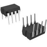
| 封装/箱体 | CDIP-8 |
| 工作电源电压 | 9 V to 36 V |
| 工厂包装数量 | 48 |
| 最大功率耗散 | 1300 mW |
| 最大双重电源电压 | +/- 18 V |
| 最大工作温度 | + 125 C |
| 最小双重电源电压 | +/- 4.5 V |
| 最小工作温度 | - 55 C |
| 电压增益dB | 70.88 dB |
| 电源电压-最大 | 36 V |
| 电源电压-最小 | 9 V |
| 电源电流 | 13.5 mA |
| 电源类型 | Dual |
| 系列 | AD827 |
| 转换速度 | 200 V/us at +/- 5 V |
| 输入偏压电流—最大 | 7 uA |
| 输入补偿电压 | 500 uV |
| 输出类型 | No |
| 通道数量 | 2 Channel |


- 商务部:美国ITC正式对集成电路等产品启动337调查
- 曝三星4nm工艺存在良率问题 高通将骁龙8 Gen1或转产台积电
- 太阳诱电将投资9.5亿元在常州建新厂生产MLCC 预计2023年完工
- 英特尔发布欧洲新工厂建设计划 深化IDM 2.0 战略
- 台积电先进制程称霸业界 有大客户加持明年业绩稳了
- 达到5530亿美元!SIA预计今年全球半导体销售额将创下新高
- 英特尔拟将自动驾驶子公司Mobileye上市 估值或超500亿美元
- 三星加码芯片和SET,合并消费电子和移动部门,撤换高东真等 CEO
- 三星电子宣布重大人事变动 还合并消费电子和移动部门
- 海关总署:前11个月进口集成电路产品价值2.52万亿元 增长14.8%


PDF Datasheet 数据手册内容提取
a High Speed, Low Power Dual Op Amp AD827 CONNECTION DIAGRAMS FEATURES High Speed 8-Lead Plastic (N) and Cerdip 16-Lead Small Outline 50 MHz Unity Gain Stable Operation (Q) Packages (R) Package 300 V/ms Slew Rate 120 ns Settling Time Drives Unlimited Capacitive Loads Excellent Video Performance 0.04% Differential Gain @ 4.4 MHz 0.198 Differential Phase @ 4.4 MHz Good DC Performance 2 mV max Input Offset Voltage 15 mV/8C Input Offset Voltage Drift Available in Tape and Reel in Accordance with EIA-481A Standard Low Power Only 10 mA Total Supply Current for Both Amplifiers 20-Lead LCC (E) Package (cid:1)5 V to (cid:1)15 V Supplies PRODUCT DESCRIPTION The AD827 is a dual version of Analog Devices’ industry- standard AD847 op amp. Like the AD847, it provides high speed, low power performance at low cost. The AD827 achieves a 300 V/µs slew rate and 50 MHz unity-gain bandwidth while consuming only 100 mW when operating from ±5 volt power supplies. Performance is specified for operation using ±5 V to ±15 V power supplies. The AD827 offers an open-loop gain of 3,500 V/V into 500 Ω loads. It also features a low input voltage noise of 15 nV/√Hz, and a low input offset voltage of 2 mV maximum. Common- mode rejection ratio is a minimum of 80 dB. Power supply APPLICATION HIGHLIGHTS rejection ratio is maintained at better than 20 dB with input 1. Performance is fully specified for operation using ±5 V to frequencies as high as 1 MHz, thus minimizing noise ±15 V supplies. feedthrough from switching power supplies. 2. A 0.04% differential gain and 0.19° differential phase error at The AD827 is also ideal for use in demanding video applica- the 4.4 MHz color subcarrier frequency, together with its low tions, driving coaxial cables with less than 0.04% differential cost, make it ideal for many video applications. gain and 0.19° differential phase errors for 643 mV p-p into a 3. The AD827 can drive unlimited capacitive loads, while its 75 Ω reverse terminated cable. 30 mA output current allows 50 Ω and 75 Ω reverse- The AD827 is also useful in multichannel, high speed data terminated loads to be driven. conversion systems where its fast (120 ns to 0.1%) settling time 4. The AD827’s 50 MHz unity-gain bandwidth makes it an is of importance. In such applications, the AD827 serves as an ideal candidate for multistage active filters. input buffer for 8-bit to 10-bit A/D converters and as an output 5. The AD827 is available in 8-lead plastic mini-DIP and cerdip, amplifier for high speed D/A converters. 20-lead LCC, and 16-lead SOIC packages. Chips and MIL-STD-883B processing are also available. REV. C Information furnished by Analog Devices is believed to be accurate and reliable. However, no responsibility is assumed by Analog Devices for its use, nor for any infringements of patents or other rights of third parties that One Technology Way, P.O. Box 9106, Norwood, MA 02062-9106, U.S.A. may result from its use. No license is granted by implication or otherwise Tel: 781/329-4700 www.analog.com under any patent or patent rights of Analog Devices. Fax: 781/326-8703 © Analog Devices, Inc., 2002
AD827–SPECIFICATIONS (@ T = +25(cid:2)C, unless otherwise noted.) A AD827J AD827A/S Model Conditions V Min Typ Max Min Typ Max Unit S DC PERFORMANCE Input Offset Voltage1 ±5 V 0.5 2 0.3 2 mV T to T 3.5 4 mV MIN MAX ±15 V 4 4 mV T to T 6 6 mV MIN MAX Offset Voltage Drift ±5 V to ±15 V 15 15 µV/°C Input Bias Current ±5 V to ±15 V 3.3 7 3.3 7 µA T to T 8.2 9.5 µA MIN MAX Input Offset Current ±5 V to ±15 V 50 300 50 300 nA T to T 400 400 nA MIN MAX Offset Current Drift ±5 V to ±15 V 0.5 0.5 nA/°C Common-Mode Rejection Ratio V = ±2.5 V ±5 V 78 95 80 95 dB CM V = ±12 V ±15 V 78 95 80 95 dB CM T to T ±5 V to ±15 V 75 75 dB MIN MAX Power Supply Rejection Ratio ±5 V to ±15 V 75 86 75 86 dB T to T 72 72 dB MIN MAX Open-Loop Gain V = ±2.5 V ±5 V O R = 500 Ω 2 3.5 2 3.5 V/mV LOAD T to T 1 1 V/mV MIN MAX R = 150 Ω 1.6 1.6 V/mV LOAD V = ±10 V ±15 V OUT R = 1 kΩ 3 5.5 3 5.5 V/mV LOAD T to T 1.5 1.5 V/mV MIN MAX MATCHING CHARACTERISTICS Input Offset Voltage ±5 V 0.4 0.2 mV Crosstalk f = 5 MHz ±5 V 85 85 dB DYNAMIC PERFORMANCE Unity-Gain Bandwidth ±5 V 35 35 MHz ±15 V 50 50 MHz Full Power Bandwidth2 V = 5 V p-p, O R = 500 Ω ±5 V 12.7 12.7 MHz LOAD V = 20 V p-p, O R = 1 kΩ ±15 V 4.7 4.7 MHz LOAD Slew Rate3 R = 500 Ω ±5 V 200 200 V/µs LOAD R = 1 kΩ ±15 V 300 300 V/µs LOAD Settling Time to 0.1% A = –1 V –2.5 V to +2.5 V ±5 V 65 65 ns –5 V to +5 V ±15 V 120 120 ns Phase Margin C = 10 pF ±15 V LOAD R = 1 kΩ 50 50 Degrees LOAD Differential Gain Error f = 4.4 MHz ±15 V 0.04 0.04 % Differential Phase Error f = 4.4 MHz ±15 V 0.19 0.19 Degrees Input Voltage Noise f = 10 kHz ±15 V 15 15 nV/√Hz Input Current Noise f = 10 kHz ±15 V 1.5 1.5 pA/√Hz Input Common-Mode Voltage Range ±5 V +4.3 +4.3 V –3.4 –3.4 V ±15 V +14.3 +14.3 V –13.4 –13.4 V Output Voltage Swing R = 500 Ω ±5 V 3.0 3.6 3.0 3.6 ±V LOAD R = 150 Ω ±5 V 2.5 3.0 2.5 3.0 ±V LOAD R = 1 kΩ ±15 V 12 13.3 12 13.3 ±V LOAD R = 500 Ω ±15 V 10 12.2 10 12.2 ±V LOAD Short-Circuit Current Limit ±5 V to ±15 V 32 32 mA INPUT CHARACTERISTICS Input Resistance 300 300 kΩ Input Capacitance 1.5 1.5 pF –2– REV. C
AD827 AD827J AD827A/S Model Conditions V Min Typ Max Min Typ Max Unit S OUTPUT RESISTANCE Open Loop 15 15 Ω POWER SUPPLY Operating Range ±4.5 ±18 ±4.5 ±18 V Quiescent Current ±5 V 10 13 10 13 mA T to T 16 16.5/17.5 mA MIN MAX ±15 V 10.5 13.5 10.5 13.5 mA T to T 16.5 17/18 mA MIN MAX TRANSISTOR COUNT 92 92 NOTES 1Offset voltage for the AD827 is guaranteed after power is applied and the device is fully warmed up. All other specifications are measured using high speed test equipment, approximately 1 second after power is applied. 2Full Power Bandwidth = Slew Rate/2 π V . PEAK 3Gain = +1, rising edge. All min and max specifications are guaranteed. Specifications subject to change without notice. ABSOLUTE MAXIMUM RATINGS1 ORDERING GUIDE Supply Voltage . . . . . . . . . . . . . . . . . . . . . . . . . . . . . . . .±18 V Internal Power Dissipation2 Temperature Package Package Plastic (N) Package (Derate at 10 mW/°C) . . . . . . . . 1.5 W Model Range Description Option Cerdip (Q) Package (Derate at 8.7 mW/°C) . . . . . . . 1.3 W AD827JN 0°C to +70°C 8-Lead Plastic DIP N-8 Small Outline (R) Package (Derate at 10 mW/°C) . . . 1.5 W AD827JR 0°C to +70°C 16-Lead Plastic SO R-16 LCC (E) Package (Derate at 6.7 mW/°C) . . . . . . . . . 1.0 W AD827AQ –40°C to +85°C 8-Lead Cerdip Q-8 Input Common-Mode Voltage . . . . . . . . . . . . . . . . . . . . .±V AD827SQ –55°C to +125°C 8-Lead Cerdip Q-8 S Differential Input Voltage . . . . . . . . . . . . . . . . . . . . . . . . . 6 V AD827SQ/883B –55°C to +125°C 8-Lead Cerdip Q-8 Output Short Circuit Duration3 . . . . . . . . . . . . . . . . Indefinite 5962-9211701MPA –55°C to +125°C 8-Lead Cerdip Q-8 Storage Temperature Range (N, R) . . . . . . . –65°C to +125°C AD827SE/883B –55°C to +125°C 20-Lead LCC E-20A Storage Temperature Range (Q) . . . . . . . . . –65°C to +150°C 5962-9211701M2A –55°C to +125°C 20-Lead LCC E-20A AD827JR-REEL 0°C to +70°C Tape & Reel Operating Temperature Range AD827JChips 0°C to +70°C Die AD827J . . . . . . . . . . . . . . . . . . . . . . . . . . . . . . 0°C to 70°C AD827SChips –55°C to +125°C Die AD827A . . . . . . . . . . . . . . . . . . . . . . . . . . . –40°C to +85°C AD827S . . . . . . . . . . . . . . . . . . . . . . . . . . –55°C to +125°C METALLIZATION PHOTOGRAPH Lead Temperature Range (Soldering to 60 sec) . . . . . . . . . . . . . . . . . . . . . . . . .300°C Contact factory for latest dimensions. Dimensions shown in inches and (mm). NOTES Substrate is connected to V+. 1Stresses above those listed under Absolute Maximum Ratings may cause perma- nent damage to the device. This is a stress rating only, and functional operation of the device at these or any other conditions above those indicated in the operational section of this specification is not implied. Exposure to absolute maximum ratings for extended periods may affect device reliability. 2Maximum internal power dissipation is specified so that T does not exceed 175°C J at an ambient temperature of 25°C. Thermal Characteristics: MiniDIP: θ = 100°C/W; θ = 33°C/ W JA JC Cerdip: θ = 110°C/W; θ = 30°C/W JA JC 16-Lead Small Outline Package: θ = 100°C/W JA 20-Lead LCC: θ = 150°C/W; θ = 35°C/W JA JC 3Indefinite short circuit duration is only permissible as long as the absolute maximum power rating is not exceeded. REV. C –3–
AD827–Typical Performance Characteristics (@ +25(cid:2)C & (cid:1)15 V, unless otherwise noted) 20 20 RANGE – Volts15 +VIN WING – Volts15 +VOUT ODE 10 GE S10 ON-M –VIN OLTA –VOUT M V T COM 5 UTPUT 5 RLOAD = 1kΩ U O P N I 0 0 0 5 10 15 20 0 5 10 15 20 SUPPLY VOLTAGE ± Volts SUPPLY VOLTAGE ± Volts Figure1.InputCommon-Mode Figure 2.Output Voltage Figure 3.Output Voltage Range vs. Supply Voltage Swing vs. Supply Voltage Swing vs. Load Resistance Figure 4.Quiescent Current Figure 5.Input Bias Current Figure 6.Closed-Loop Output vs. Supply Voltage vs. Temperature Impedance vs. Frequency, Gain = +1 14 A12 m ENT – VS = ±15V R R U NT C10 VS = ±5V E C S E UI Q 8 0 –60 –40 –20 0 20 40 60 80 100 120 140 TEMPERATURE – °C Figure 7.Quiescent Current Figure 8.Short-Circuit Figure 9.Gain Bandwidth vs. vs. Temperature Current Limit vs. Temperature Temperature –4– REV. C
AD827 Figure 12.Power Supply Rejection Figure 10.Open-Loop Gain and Figure 11.Open-Loop Gain Ratio vs. Frequency Phase Margin vs. Frequency vs. Load Resistance Figure 15.Output Swing and Figure 13.Common-Mode Figure 14.Large Signal Error vs. Settling Time Rejection Ratio vs. Frequency Frequency Response 400 RISE 350 AV = +1 SLEW RATE 10 – 90% s/µs 300 FALL – Volt VS = ±15V ATE 250 RISE R W LE 200 S VS = ±5V FALL 150 100 –60 –40 –20 0 20 40 60 80 100 120 140 TEMPERATURE – °C Figure 16.Harmonic Distortion Figure 17.Input Voltage Figure 18.Slew Rate vs. vs. Frequency Noise Spectral Density Temperature REV. C –5–
AD827 Figure 19.Crosstalk vs. Frequency Figure 20.Crosstalk Test Circuit INPUT PROTECTION PRECAUTIONS For high performance circuits, it is recommended that a second An input resistor (resistor R of Figure 21a) is recommended in resistor (R in Figures 21a and 22a) be used to reduce bias- IN B circuits where the input common-mode voltage to the AD827 current errors by matching the impedance at each input. This may exceed (on a transient basis) the positive supply voltage. resistor reduces the error caused by offset voltages by more than This resistor provides protection for the input transistors by an order of magnitude. limiting the maximum current that can be forced into their bases. Figure 21b.Follower Large Figure 21c.Follower Small Figure 21a.Follower Connection Signal Pulse Response Signal Pulse Response Figure 22b.Inverter Large Figure 22c.Inverter Small Figure 22a.Inverter Connection Signal Pulse Response Signal Pulse Response –6– REV. C
AD827 VIDEO LINE DRIVER A HIGH SPEED THREE OP AMP INSTRUMENTATION The AD827 functions very well as a low cost, high speed line AMPLIFIER CIRCUIT driver for either terminated or unterminated cables. Figure 23 The instrumentation amplifier circuit shown in Figure 24 can shows the AD827 driving a doubly terminated cable in a provide a range of gains. Table II details performance. follower configuration. +VS TRIM FOR BEST +VS 0.1µF SETTLING TIME 2 – 8pF VIN 0.1 µF –VIN 3 +1/28 1 2kΩ 50Ω AD18/227 R 5B0TΩ RT VOUT 2 A–D18k2Ω7 +VS0.1µF 0.1 µF 500Ω 50Ω RG TORPITMIM FUOMR 2kΩ 2 –AD7847 6 –VS BA7N –D 1W5 IpDFTH 2kΩ3pF 2k3Ω+ 4 0.1µF 2RkΩLVOUT 1kΩ 6 – CC 500Ω +VIN 5+AD1/822470.1µ7F CIRCUI–TV GSAIN =2000+ 1 RG –VS NOTE: PINOUT SHOWN IS FOR MINIDIP PACKAGE Figure 23.A Video Line Driver Figure 24.A High Bandwidth Three Op Amp The termination resistor, R , (when equal to the cable’s Instrumentation Amplifier T characteristic impedance) minimizes reflections from the far end of the cable. While operating from ±5 V supplies, the AD827 Table II. Performance Specifications for the maintains a typical slew rate of 200 V/µs, which means it can Three Op Amp Instrumentation Amplifier drive a ±1 V, 30 MHz signal into a terminated cable. Small Signal Table I. Video Line Driver Performance Summary Bandwidth Gain R @ 1 V p-p Output G Over- 1 Open 16.1 MHz V * V C –3 dB B shoot IN SUPPLY C W 2 2 k 14.7 MHz 0 dB or ±500 mV Step ±15 20 pF 23 MHz 4% 10 226 Ω 4.9 MHz 0 dB or ±500 mV Step ±15 15 pF 21 MHz 0% 100 20 Ω 660 kHz 0 dB or ±500 mV Step ±15 0 pF 13 MHz 0% 0 dB or ±500 mV Step ±5 20 pF 18 MHz 2% 0 dB or ±500 mV Step ±5 15 pF 16 MHz 0% 0 dB or ±500 mV Step ±5 0 pF 11 MHz 0% *–3 dB bandwidth numbers are for the 0 dBm signal input. Overshoot numbers are the percent overshoot of the 1 V step input. A back-termination resistor (R , also equal to the characteristic BT impedance of the cable) may be placed between the AD827 output and the cable input, in order to damp any reflected signals caused by a mismatch between R and the cable’s T characteristic impedance. This will result in a flatter frequency response, although this requires that the op amp supply ±2 V to the output in order to achieve a ±1 V swing at resistor R . T REV. C –7–
AD827 A TWO-CHIP VOLTAGE-CONTROLLED AMPLIFIER between the CH1 output and Z1, the other between the CH1 (VCA) WITH EXPONENTIAL RESPONSE output and W1. Likewise, in the CH2 multiplier, one of the Voltage-controlled amplifiers are often used as building blocks feedback resistors is connected between CH2 and Z2 and the in automatic gain control systems. Figure 25 shows a two-chip other is connected between CH2 and Z2. In Figure 25, Z1 and VCA built using the AD827 and the AD539, a dual, current- W1 are tied together, as are Z2 and W2, providing a 3 kΩ output multiplier. As configured, the circuit has its two feedback resistor for the op amp. The 2 pF capacitors connected between the AD539’s W1 and CH1 and W2 and CH2 pins are in parallel with the feedback resistors and thus reduce peaking in the VCA’s frequency response. Increasing the values of C3 and C4 can further reduce the peaking at the expense of reduced bandwidth. The 1.25 mA full-scale output current of the AD539 and the 3 kΩ feedback resistor set the full-scale output voltage of each multiplier at 3.25 V p-p. Current limiting in the AD827 (typically 30 mA) limits the out- put voltage in this application to about 3 V p-p across a 100Ω load. Driving a 50 Ω reverse-terminated load divides this value by two, limiting the maximum signal delivered to a 50Ω load to about 1.5 V p-p, which suffices for video signal levels. The dynamic range of this circuit is approximately 55dB and is primarily limited by feedthrough at low input levels and by the maximum output voltage at high levels. Figure 25.A Wide Range Voltage-Controlled Guidelines for Grounding and Bypassing Amplifier Circuit When designing practical high frequency circuits using the AD827, some special precautions are in order. Both short interconnection leads and a large ground plane are needed whenever possible to multipliers connected in series. They could also be placed in provide low resistance, low inductance circuit paths. One should parallel with an increase in bandwidth and a reduction in gain. remember to minimize the effects of capacitive coupling The gain of the circuit is controlled by V , which can range X between circuits. Furthermore, IC sockets should be avoided. from 0 to 3 V dc. Measurements show that this circuit easily Feedback resistors should be of a low enough value that the supplies 2 V p-p into a 100 Ω load while operating from ±5 V time constant formed with stray circuit capacitances at the supplies. The overall bandwidth of the circuit is approximately amplifier summing junction will not limit circuit performance. 7 MHz with 0.5 dB of peaking. As a rule of thumb, use feedback resistor values that are less Each half of the AD827 serves as an I/V converter and converts than 5 kΩ. If a larger resistor value is necessary, a small (<10pF) the output current of one of the two multipliers in the AD539 feedback capacitor in parallel with the feedback resistor may be into an output voltage. Each of the AD539’s two multipliers used. The use of 0.1 µF ceramic disc capacitors is recommended contains two internal 6 kΩ feedback resistors; one is connected for bypassing the op amp’s power supply leads. –8– REV. C
AD827 OUTLINE DIMENSIONS 8-Lead Plastic Dual-in-Line Package [PDIP] 8-Lead Ceramic DIP-Glass Hermetic Seal Package [CERDIP] (N-8) (Q-8) Dimensions shown in millimeters and (inches) Dimensions shown in millimeters and (inches) 10.92 (0.4299) 0.13 (0.0051)1.40 (0.0551) 8.84 (0.3480) MIN MAX 8 5 8 5 7.11 (0.2799) 7.87 (0.3089) 6.10 (0.2402) 1 4 PIN 1 5.59 (0.2201) 1 4 PIN 1 8.25 (0.3248) 2.54 (0.1000) 7.62 (0.3000) 2.54 (0.1000) BSC BSC 10.29 (0.4051) MAX 8.13 (0.3201) 5.33 1.52 (0.0598) 4.95 (0.1949) 1.52 (0.0600) 7.37 (0.2902) (0.2098) 0.38 (0.0150) 2.93 (0.1154) 5.08 (0.2000) 0.38 (0.0150) MAX ( 3.30 MAX 4.06 (0.1598) (0.1299) 0.38 (0.0150) 2.93 (0.1154) MIN 0.20 (0.0079) 53..0188 ((00..21020502)) 3M.I8N1 (0.1500) 0.56 (0.0220) SEATING 0.36 (0.0142) 11..7175 ((00..00649573)) PLANE 00..5386 ((00..00212482)) 10..7786 ((00..00720919))SPELAANTIENG 1 05 00..3280 ((00..00105709)) CONTROLLING DIMENSIONS ARE IN MILLIMETERS; INCH DIMENSIONS (IN PARENTHESES) ARE ROUNDED-OFF MILLIMETER EQUIVALENTS FOR CONTROLLING DIMENSIONS ARE IN MILLIMETERS; INCH DIMENSIONS REFERENCE ONLY AND ARE NOT APPROPRIATE FOR USE IN DESIGN (IN PARENTHESES) ARE ROUNDED-OFF MILLIMETER EQUIVALENTS FOR REFERENCE ONLY AND ARE NOT APPROPRIATE FOR USE IN DESIGN 16-Lead Standard Small Outline Package [SOIC] 20-Terminal Ceramic Leadless Chip Carrier [LCC] Wide Body (E-20A) (R-16) Dimensions shown in millimeters and (inches) Dimensions shown in millimeters and (inches) 1.91 5.08 (0.2000) (0.0752) BSC 10.50 (0.4134) 2.54 (0.1000) REF 10.10 (0.3976) 1.63 (0.0642) 2.41 (0.0949) 2.54 (0.1000) BSC 1.90 (0.0748) 0.38 (0.0150) 19 3 MIN 16 9 18 20 4 0.71 (0.0278) 1 8 77..6400 ((00..2211990091..602350)) ((00..43199337)) 98..0699 S((00Q..33547291))(0.3M59S7.A09QX9) 100.9..21188 R( 0(( 00.T0..Y007RP105E172F01))) 1314BOVTIE1TWOM89 1B.S02.C75 6(0 (.00.500202)0) 45 TYP 2.24 (0.0882) 1.40 (0.0551) 3.81 (0.1500) PIN 1 1.27B (0S.C0500) 22..6355 ((00..10094235)) 00..7255 ((00..00209958))(cid:3) 45(cid:2) CON1T.3R7O (L0L.0IN53G9 )DIMENSIONS1 .A1R4 E(0 I.N04 M49IL)LIMETERS; INBCSHC DIMENSIONS 0.30 (0.0118) (IN PARENTHESES) ARE ROUNDED-OFF MILLIMETER EQUIVALENTS FOR 0.10 (0.0039) REFERENCE ONLY AND ARE NOT APPROPRIATE FOR USE IN DESIGN 8(cid:2) COPL0A.1N0ARITY 00..5313 ((00..00210310)) SPELAANTIENG 00..3223 ((00..00102961)) 0(cid:2) 10..2470 ((00..00510507)) CONTROLLING DIMENSIONS ARE IN MILLIMETERS; INCH DIMENSIONS (IN PARENTHESES) ARE ROUNDED-OFF MILLIMETER EQUIVALENTS FOR REFERENCE ONLY AND ARE NOT APPROPRIATE FOR USE IN DESIGN COMPLIANT TO JEDEC STANDARDS MS-013AA REV. C –9–
AD827 Revision History Location Page 8/02—Data Sheet changed from REV. B to REV. C. Updated Outline Dimensions . . . . . . . . . . . . . . . . . . . . . . . . . . . . . . . . . . . . . . . . . . . . . . . . . . . . . . . . . . . . . . . . . . . . . . . . . . . . . .9 –10– REV. C
–11–
C) 2( 0 8/ – 0 – 8 7 8 0 0 C A. S. U. N D I E T N RI P –12–