
 Datasheet下载
- 型号: 500R14N331JV4T
- 制造商: Johanson Dielectrics Inc.
- 库位|库存: xxxx|xxxx
- 要求:
| 数量阶梯 | 香港交货 | 国内含税 |
| +xxxx | $xxxx | ¥xxxx |
查看当月历史价格
查看今年历史价格
500R14N331JV4T产品简介:
ICGOO电子元器件商城为您提供500R14N331JV4T由Johanson Dielectrics Inc.设计生产,在icgoo商城现货销售,并且可以通过原厂、代理商等渠道进行代购。 500R14N331JV4T价格参考¥0.64-¥3.35。Johanson Dielectrics Inc.500R14N331JV4T封装/规格:陶瓷电容器, 330pF ±5% 50V 陶瓷电容器 C0G,NP0 0603(1608 公制)。您可以下载500R14N331JV4T参考资料、Datasheet数据手册功能说明书,资料中有500R14N331JV4T 详细功能的应用电路图电压和使用方法及教程。
Johanson Dielectrics Inc. 生产的陶瓷电容器型号为 500R14N331JV4T,属于高频应用领域的片式多层陶瓷电容器(MLCC)。以下是该型号可能的应用场景:

 1. 射频滤波与匹配电路
   - 该型号电容器适用于射频(RF)前端模块中的滤波和阻抗匹配电路。其高Q值特性和低等效串联电阻(ESR)使其适合用于无线通信设备中,如蜂窝基站、Wi-Fi路由器、蓝牙模块等。
   - 在射频滤波器中,可有效去除不需要的频率成分,确保信号的纯净性。

 2. 谐振电路
   - 在射频谐振电路中,该电容器常与电感配合使用,形成LC谐振回路。这种应用场景常见于无线通信系统、雷达设备以及无线能量传输装置。

 3. 电源去耦
   - 在高频电源设计中,该电容器可用于去耦以抑制噪声和干扰。例如,在射频放大器或高速数字电路中,它能稳定电压并减少高频纹波。

 4. 天线调谐
   - 在天线设计中,此型号电容器可以用来调整天线的谐振频率,优化其在特定频段内的性能。这在移动通信设备、物联网(IoT)设备和卫星通信系统中非常常见。

 5. 无线能量传输
   - 在无线充电系统中,该电容器可用于调节谐振频率,提高能量传输效率,并减少电磁干扰(EMI)。

 6. 航空航天与国防
   - Johanson Dielectrics 的产品以其高可靠性和稳定性著称,因此该型号也可能应用于航空航天和国防领域,例如卫星通信、雷达系统和军用无线电设备。

 总结
型号 500R14N331JV4T 的陶瓷电容器凭借其优异的高频性能和可靠性,广泛应用于射频通信、无线技术、电源管理和高端工业及军事领域。具体选择时需结合实际电路需求和工作环境进行评估。
| 参数 | 数值 |
| 产品目录 | |
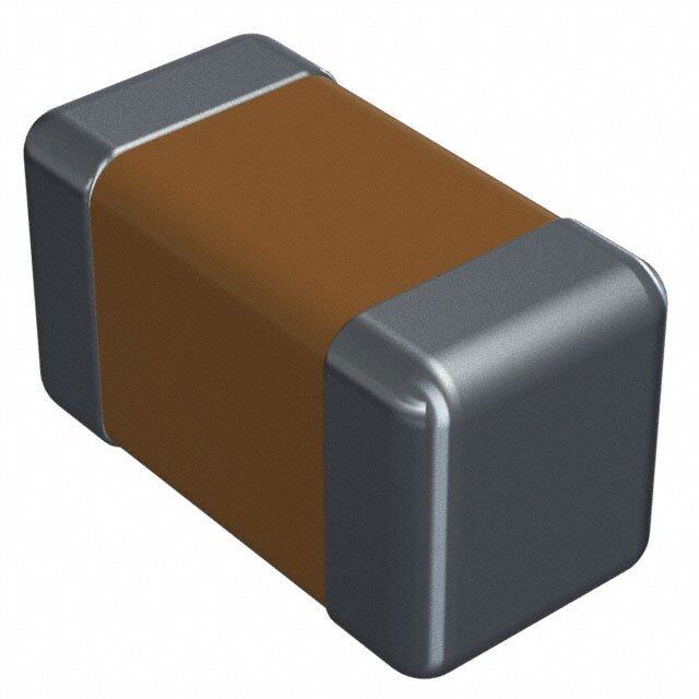
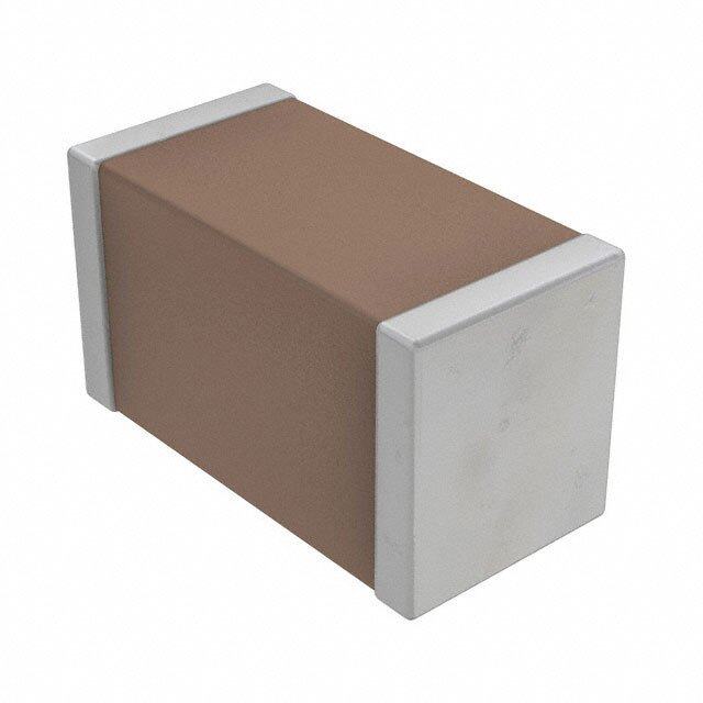
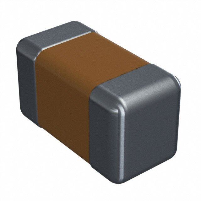
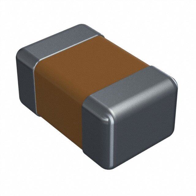
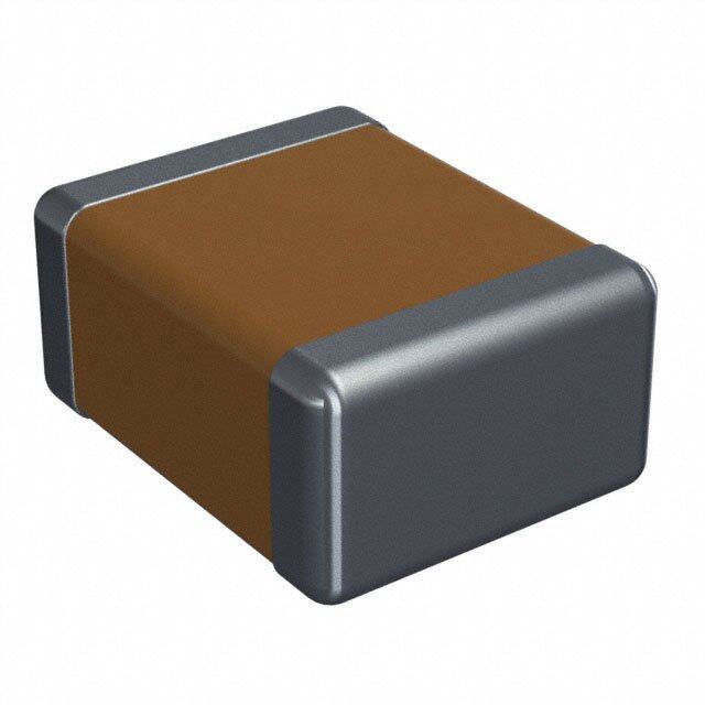
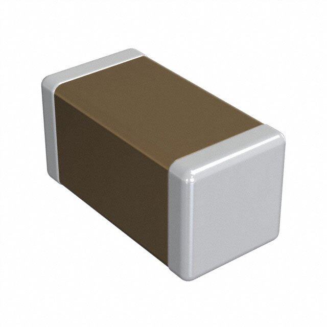
| 描述 | CAP CER 330PF 50V 5% NP0 0603 |
| 产品分类 | |
| 品牌 | Johanson Dielectrics Inc |
| 数据手册 | |
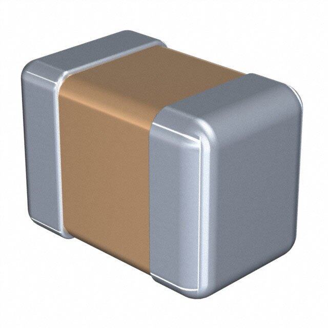
| 产品图片 |
|
| 产品型号 | 500R14N331JV4T |
| rohs | 无铅 / 符合限制有害物质指令(RoHS)规范要求 |
| 产品系列 | - |
| 产品目录绘图 |
|
| 产品目录页面 | |
| 其它名称 | 709-1149-1 |
| 包装 | 剪切带 (CT) |
| 厚度(最大值) | 0.035"(0.89mm) |
| 大小/尺寸 | 0.063" 长 x 0.032" 宽(1.60mm x 0.81mm) |
| 安装类型 | 表面贴装,MLCC |
| 容差 | ±5% |
| 封装/外壳 | 0603(1608 公制) |
| 工作温度 | -55°C ~ 125°C |
| 工具箱 | /product-detail/zh/S-0603-DIGI/709-1110-ND/1859442 |
| 应用 | 通用 |
| 引线形式 | - |
| 引线间距 | - |
| 标准包装 | 1 |
| 温度系数 | C0G,NP0 |
| 特性 | - |
| 电压-额定 | 50V |
| 电容 | 330pF |
| 等级 | - |
| 高度-安装(最大值) | - |


- 商务部:美国ITC正式对集成电路等产品启动337调查
- 曝三星4nm工艺存在良率问题 高通将骁龙8 Gen1或转产台积电
- 太阳诱电将投资9.5亿元在常州建新厂生产MLCC 预计2023年完工
- 英特尔发布欧洲新工厂建设计划 深化IDM 2.0 战略
- 台积电先进制程称霸业界 有大客户加持明年业绩稳了
- 达到5530亿美元!SIA预计今年全球半导体销售额将创下新高
- 英特尔拟将自动驾驶子公司Mobileye上市 估值或超500亿美元
- 三星加码芯片和SET,合并消费电子和移动部门,撤换高东真等 CEO
- 三星电子宣布重大人事变动 还合并消费电子和移动部门
- 海关总署:前11个月进口集成电路产品价值2.52万亿元 增长14.8%

PDF Datasheet 数据手册内容提取
R o H CoS/ mR Ceramic pliE aA ncC eH Component Solutions AC Safety Certified High Voltage SMT High Capacitance High Temperature EMI Filters (X2Y®) LICC Low ESL SMPS Stacks High Voltage Radials Precision Power Resistors Power Inductors Planar Array Discoidal CapStrate® Custom Solutions
Y T P OUR ECHNOLOGY ARTNER The mission of the Johanson Companies is to Customized solutions in the areas of High Tem- translate our customer needs into quality electronic perature and High AC power ceramic capacitors are components, produced in factories that are models available to customers who require a partnered tech- of excellence, supported by innovative service. With nology solution. over 30 years of experience, Johanson Dielectrics Johanson Dielectrics design and manufacturing provides both standard and custom technology solu- operations are located in Sylmar, California and tions tailored to your specific electronic applications. Zhoaqing, PRC. Our quality minded management Our standard product range includes High Voltage system utilizes continuous improvement programs and AC Safety Capacitors providing solutions for focused on increased product reliability, manufac- Lighting, IT and Business Equipment designs. Our turing through-put, and product performance. Our X2Y® Capacitor line provides advanced EMI fil- broad experience, applications support, and respon- tering and IC decoupling solutions and our High sive service enhance our ability to drive down your Capacitance Tanceram® products provide the highest total cost of procurement and speed your time to capacitance values in the smallest cases sizes. market. HIGH FREQUENCY CERAMIC SOLUTIONS Johanson Technology Inc., Camarillo CA. Products include High Q Capacitors, Ceramic and Wire- wound Chip Inductors, and a broad range of LTCC based RF IPCs such as Antennas, Filters, Baluns, Couplers, Matched Filter Baluns, etc. www.johansontechnology.com Johanson Dielectrics, Inc. reserves the right to make design and price changes without notice. All sales are subject to the Johanson terms and conditions, including a limited warranty and remedies for non- conforming goods or defective goods. Download the Johanson terms and conditions from our website at https://www.johansondielectrics.com/terms-and-conditions. 2 www.johansondielectrics.com
I P NDEX OF RODUCTS SURFACE MOUNT CERAMIC CAPACITORS Ceramic Capacitor Prototyping Kits 4-5 High Voltage Capacitors 250 - 6,000 VDC 6-7 Safety Capacitors 250 VAC, Y2, X1, X2 8-9 EMI - X2Y® Filter & Decoupling Capacitors 10-13 Low Inductance Capacitors 14 Chip Feedthru Filter Capacitors 15 High Temperature 200°C Capacitors 16-17 High Capacitance Tanceram® Capacitors 18-19 SMT Multi-layer Ceramic Capacitors 10 - 200 VDC 20-21 LEADED CERAMIC CAPACITORS SMPS Stacked Capacitors, 125°C & 200°C versions 22-23 Mini-SMPS Stacked Capacitors 24-25 BME Mini SMPS Capacitors 26-27 Switch-mode Radial Leaded Capacitors 28-29 High Voltage Radial Leaded Capacitors, 125°C, 200°C versions 30-31 PRECISION POWER RESISTORS Resistor Wirewound Precision 32-33 Resistor Wirewound Precision SMT 34-35 Resistor Wirewound High Power Rating 36-39 Resistor Wirewound Chassis Mount 40-42 Resistor Thin Film Precision 43-46 Resistor Metal Element Current Sense SMT 47-49 Resistor High Power Low Inductance 50-53 Resistor Thick Film, High Temperature 54-56 Resistor Metal Element Current Sense 57-58 Resistor Power Thin Film 59-61 POWER INDUCTORS Semi-shielded (Coated) & Shielded 62-69 Shielded LPM Series 70-74 PLANAR CAPACITORS & CUSTOM CERAMIC SOLUTIONS Planar Array Capacitors 75-76 CAPSTRATE & CUSTOMER CERAMIC SOLUTIONS CapStrate® & Customer Ceramic Solutions 77-78 PART NUMBER, DIELECTRIC, PACKAGING SPECIFICATIONS Capacitor General Electrical Characteristics and PN breakdown 79 www.johansondielectrics.com 3
C C E D K ERAMIC APACITOR NGINEERING ESIGN ITS Johanson Dielectrics, Inc. offers a variety of multi-layer chip capacitor sample kits for proto-type design work. Each kit is grouped by type, size, or voltage and contains a selection of popular values and tolerances. The chips are individually packaged in labeled plastic compartments for easy access. The general range of kit contents is described below. Specific part number details may be found at www.johansondielectrics.com 0402 Ceramic Chip Capacitor Kit P/N: S-0402 1400 piece sample assortment of selected values from 1.0pF to 0.22µF Chip Size Voltage Rating Dielectric Capacitance Range Qty / Value Total Qty 0402 50 VDC - 6.3 VDC NP0, X7R 1.0pF to 0.22µF 50 pcs 1400 pcs 0603 Ceramic Chip Capacitor Kit P/N: S-0603 1400 piece sample assortment of selected values from 1.0pF to 0.22µF Chip Size Voltage Rating Dielectric Capacitance Range Qty / Value Total Qty 0603 50 VDC - 16 VDC NP0, X7R 10pF to 0.22µF 50 pcs 1400 pcs 0805 Ceramic Chip Capacitor Kit P/N: S-0805 1400 piece sample assortment of selected values from 1.0pF to 0.47µF Chip Size Voltage Rating Dielectric Capacitance Range Qty / Value Total Qty 0805 100 VDC - 16 VDC NP0, X7R 10pF to 0.47µF 50 pcs 1400 pcs 500 VDC Ceramic Chip Capacitor Kit P/N: S-500 400 piece sample assortment of selected values from 33pF to 0.1µF Chip Size Voltage Rating Dielectric Capacitance Range Qty / Value Total Qty 0805 - 1812 500 VDC NP0, X7R 33pF to 0.1µF 10-20 pcs 400 pcs 1000 VDC Ceramic Chip Capacitor Kit P/N: S-1KV 400 piece sample assortment of selected values from 22pF to 0.1µF Chip Size Voltage Rating Dielectric Capacitance Range Qty / Value Total Qty 0805 - 2225 1000 VDC NP0, X7R 22pF to 0.1µF 10-20 pcs 400 pcs Johanson may from time-time adjust actual kit contents based on design demand trends. Check the Johanson web site for design kit updates and kit content changes. 4 www.johansondielectrics.com
C C E D K ERAMIC APACITOR NGINEERING ESIGN ITS 2000 VDC Ceramic Chip Capacitor Kit P/N: S-2KV 300 piece sample assortment of selected values from 22pF to 0.022µF Chip Size Voltage Rating Dielectric Capacitance Range Qty / Value Total Qty 1206 - 2225 2000 VDC NP0, X7R 22pF to 0.022µF 10-20 pcs 300 pcs X2 SAFETY CERTIFIED Ceramic Chip Capacitor Kit P/N: S-SY3 240 piece sample assortment of selected values from 10pF to 1500 pF Chip Size Voltage Rating Dielectric Capacitance Range Qty / Value Total Qty 1808 3KV DC / 250 AC NP0, X7R 10pF to 1500 pF 20 pcs 240 pcs X1/Y2 SAFETY CERTIFIED Ceramic Chip Capacitor Kit P/N: S-SY2 200 piece sample assortment of selected values from 10pF to 2200 pF Chip Size Voltage Rating Dielectric Capacitance Range Qty / Value Total Qty 1808 - 2220 5KV DC / 250 VAC NP0, X7R 10pF to 2200pF 20 pcs 200 pcs X2Y® EMI FILTER Capacitor Kit - 0402 Size P/N: S-X07CBK 600 piece sample assortment of selected values from 1.0pF to 0.01µF Chip Size Voltage Rating Dielectric Capacitance Range Qty / Value Total Qty 0402 10 - 50 VDC NP0, X7R 1.0pF to 0.01µF 50 pcs 600 pcs X2Y® EMI FILTER Capacitor Kit - 0603 Size P/N: S-X14CBK 700 piece sample assortment of selected values from 1.0pF to 0.01µF Chip Size Voltage Rating Dielectric Capacitance Range Qty / Value Total Qty 0603 50 - 100 VDC NP0, X7R 1.0pF to 0.01µF 50 pcs 700 pcs X2Y® POWER BYPASS Capacitor Kit - 0603 Size P/N: S-X14-PBP 300 piece sample assortment of selected values from 1.0nF to 1.0µF Chip Size Voltage Rating Dielectric Capacitance Range Qty / Value Total Qty 0603 6.3 - 100 VDC X7R, X5R 1.0nF to 1.0µF 20 pcs 300 pcs X2Y® EMI FILTER Capacitor Kit - 0805 Size P/N: S-X15-EMI 300 piece sample assortment of selected values from 1.0pF to 0.01µF Chip Size Voltage Rating Dielectric Capacitance Range Qty / Value Total Qty 0805 50 - 100 VDC NP0, X7R 1.0pF to 0.01µF 20 pcs 300 pcs X2Y® AUTOMOTIVE QUALIFIED capacitor kit P/N: S-X2Y-AEC 420 piece sample assortment of selected values from 100pF to 0.22µF Chip Size Voltage Rating Dielectric Capacitance Range Qty / Value Total Qty 0603, 0805, 1206 10 - 100 VDC X7R 100pF to 0.22µF 30 pcs 420 pcs Johanson may from time-time adjust actual kit contents based on design demand trends. Check the Johanson web site for design kit updates and kit content changes. www.johansondielectrics.com 5
H V S M MLCC 250 - 6,000 VDC IGH OLTAGE URFACE OUNT S These high voltage capacitors feature a special internal electrode design which reduces voltage concentrations by distributing voltage gradients throughout the entire capacitor. This unique design also affords increased capacitance values in a given case size and voltage rating. The capacitors are designed and manufactured to the general requirement of EIA198 and are subjected to a 100% electrical testing making them well suited for a wide variety of telecommunication, commercial, and industrial applications. APPLICATIONS • Analog & Digital Modems • LAN/WAN Interface • Lighting Ballast Circuits • Voltage Multipliers • DC-DC Converters • Back-lighting Inverters Polyterm® soft termination option for demanding environments & processes available on select parts, please contact the factory. CASE SIZE CAPACITANCE SELECTION RATED NP0 DIELECTRIC X7R DIELECTRIC JDI /EIA INCHES (MM) VOLTAGE MINIMUM MAXIMUM MINIMUM MAXIMUM L .080 ±.010 (2.03 ±.25) 250 VDC - - 1000 pF 0.022 µF R15/0805 W .050 ±.010 (1.27 ±.25) 500 VDC 10 pF 680 pF 1000 pF 0.010 µF T .055 Max. (1.40) 630 VDC 10 pF 560 pF 1000 pF 6800 pF E/B .020 ±.010 (0.51±.25) 1000 VDC 10 pF 390 pF 100 pF 2700 pF 250 VDC - - 1000 pF 0.068 µF R18/1206 L .125 ±.010 (3.18 ±.25) 500 VDC 10 pF 1500 pF 1000 pF 0.033 µF W .062 ±.010 (1.57 ±.25) 630 VDC 10 pF 1200 pF 1000 pF 0.027 µF T .067 Max. (1.70) 1000 VDC 10 pF 1000 pF 100 pF 0.010 µF E/B .020 ±.010 (0.51±.25) 2000 VDC 10 pF 220 pF 100 pF 4700 pF 3000 VDC 10 pF 82 pF 100 pF 1000 pF 250 VDC - - 1000 pF 0.150 µF S41/1210 L .125 ±.010 (3.18 ±.25) 500 VDC 10 pF 3900 pF 1000 pF 0.068 µF W .095 ±.010 (2.41 ±.25) 630 VDC 10 pF 2700 pF 1000 pF 0.047 µF T .080 Max. (2.03) 1000 VDC 10 pF 1800 pF 100 pF 0.015 µF E/B .020 ±.010 (0.51±.25) 2000 VDC 10 pF 560 pF 100 pF 4700 pF 3000 VDC 10 pF 220 pF 100 pF 1000 pF 500 VDC 10 pF 4700 pF 1000 pF 0.100 µF R29/1808 630 VDC 10 pF 3300 pF 1000 pF 0.047 µF L .185 ±.020 (4.70 ±.51) 1000 VDC 1.0 pF 2200 pF 100 pF 0.022 µF W .080 ±.010 (2.03 ±.25) 2000 VDC 1.0 pF 820 pF 100 pF 0.010 µF T .085 Max. (2.16) 3000 VDC 1.0 pF 470 pF 100 pF 3300 pF E/B .020 ±.010 (0.51±.25) 4000 VDC 1.0 pF 180 pF 100 pF 1800 pF 5000 VDC 1.0 pF 75 pF 47 pF 390 pF 6000 VDC 1.0 pF 75 pF 47 pF 150 pF Available cap. values include these significant retma values and their multiples: 1.0 1.2 1.5 1.8 2.2 2.7 3.3 3.9 4.7 5.6 6.8 8.2 ( 1.0 = 1.0, 10, 100, 1000, etc.) Consult factory for non-retma values and sizes or voltages not shown. 6 www.johansondielectrics.com
H V S M MLCC 250 - 6,000 VDC IGH OLTAGE URFACE OUNT S CASE SIZE CAPACITANCE SELECTION RATED NP0 DIELECTRIC X7R DIELECTRIC JDI /EIA INCHES (MM) VOLTAGE MINIMUM MAXIMUM MINIMUM MAXIMUM 250 VDC - - 0.010µF 0.470uF S43 / 1812 500 VDC 100pF 8200pF 1000pF 0.330uF 630 VDC 100pF 6800pF 1000pF 0.120µF L .177 ±.012 (4.50 ±.30) 1000 VDC 10pF 5600pF 1000pF 0.100µF W .125 ±.010 (3.18 ±.25) 2000 VDC 10pF 1800pF 100pF 0.010µF T .110 Max. (2.80) E/B .025 ±.015 (0.64±.38) 3000 VDC 10pF 1000pF 100pF 4700pF 4000 VDC 10pF 390pF 100pF 1200pF 5000 VDC 10pF 150pF 100pF 820pF 6000 VDC 10pF 150pF 10pF 330pF 500 VDC 100pF 0.018µF 0.01µF 0.390µF S49 / 1825 630 VDC 100pF 0.015µF 0.01µF 0.270µF L .180 ±.010 (4.57 ±.25) 1000 VDC 10pF 0.012µF 1000pF 0.180µF W .250 ±.010 (6.35 ±.25) 2000 VDC 10pF 5600pF 100pF 0.039µF T .140 Max. (3.56) 3000 VDC 10pF 2200pF 100pF 8200pF E/B .025 ±.015 (0.64±.38) 4000 VDC 10pF 1200pF 100pF 2200pF 5000 VDC 10pF 390pF 100pF 1500pF 6000 VDC 10pF 390pF 100pF 820pF 500 VDC 1000pF 0.018µF 0.01µF 0.470µF S47 / 2220 630 VDC 1000pF 0.018µF 0.01µF 0.270µF L .225 ±.015 (5.72 ±.38) 1000 VDC 100pF 0.015µF 1000pF 0.120µF W .200 ±.015 (5.08 ±.38) 2000 VDC 100pF 5600pF 1000pF 0.039µF T .150 Max. (3.81) 3000 VDC 10pF 2700pF 100pF 0.010µF E/B .025 ±.015 (0.64±.38) 4000 VDC 10pF 1500pF 100pF 2700pF 5000 VDC 10pF 470pF 100pF 1500pF 6000 VDC 10pF 470pF 100pF 820pF 500 VDC 1000pF 0.027µF 0.01µF 0.560µF S48 / 2225 630 VDC 1000pF 0.022µF 0.01µF 0.390µF L .225 ±.010 (5.72 ±.25) 1000 VDC 100pF 0.018µF 1000pF 0.180µF W .255 ±.015 (6.48 ±.38) 2000 VDC 100pF 8200pF 1000pF 0.056µF T .160 Max. (4.06) 3000 VDC 10pF 3300pF 100pF 0.012µF E/B .025 ±.015 (0.64±.38) 4000 VDC 10pF 1800pF 100pF 3300pF 5000 VDC 10pF 470pF 100pF 2700pF 6000 VDC 10pF 470pF 100pF 1200pF Available cap. values include these significant retma values and their multiples: 1.0 1.2 1.5 1.8 2.2 2.7 3.3 3.9 4.7 5.6 6.8 8.2 ( 1.0 = 1.0, 10, 100, 1000, etc.) Consult factory for non-retma values and sizes or voltages not shown. ELECTRICAL CHARACTERISTICS W L Meets the standard NP0 & X7R dielectric specifications listed on page 79 DIELECTRIC WITHSTANDING VOLTAGE DWV = 1.5 X rated WVDC for ratings 500-999 WVDC, T E/B DWV = 1.2 X rated WVDC for ratings ≥ 1,000 WVDC NOTE: Capacitors may require a surface coating to prevent external arcing. Solder mask should not be used beneath capacitors. For more information see JDI Tech Note “Surface Arc Season” HOW TO ORDER HIGH VOLTAGE SURFACE MOUNT P/N written: 202R18W102KV4E 202 R18 W 102 K V 4 E VOLTAGE SIZE DIELECTRIC CAPACITANCE TOLERANCE TERMINATION MARKING PACKING 501 = 500 V R15 = 0805 N = NP0 1st two digits are signifi- J = ± 5% V = NI Barrier with 100% 4 = Unmarked E = Embossed 7” 631 = 630 V R18 = 1206 W = X7R cant; third digit denotes K = ± 10% Sn Plating (Matte) 6 = EIA Code T = Punched 7” 102 = 1000 V R29 = 1808 number of zeros. M = ± 20% 202 = 2000 V S41 = 1210 102 = 1000 pF F = Polyterm No code = bulk 302 = 3000 V S43 = 1812 104 = 0.10 µF flexible termination Tape specs. 402 = 4000 V S47 = 2220 T = SnPb per EIA RS481 502 = 5000 V S48 = 2225 602 = 6000 V S49 = 1825 www.johansondielectrics.com 7
AC S C AFETY APACITORS Johanson Dielectrics Type SC ceramic chip capacitors are designed for AC voltage surge and lightning protection in line- to-ground interface applications in computer networks, modem, facsimile and other equipment. Johanson’s safety capacitor offering includes four different case sizes in NP0 and X7R dielectric materials. These devices are surface mount ready with barrier terminations and tape and reel packaging. Information on capacitor safety ratings and certification details may be found below. Polyterm® soft termination W L option for demanding environments & processes T E/B available on select parts, please contact the factory. SAFETY VOLTAGE WITHSTANDING IMPULSE CASE JOHANSON RATING RATING VOLTAGE VOLTAGE SIZE ORDERING P/N X2 250 VAC 1,500 VAC 2,500 V 1808 302R29______V3E-****-SC STANDARDS: IEC/EN 60384-14:2013 EN 60950 2006 • UL 60384-14, UL 60950-01 CERTIFICATIONS: TUV R 50227900 & T 72140662 • UL File E472557 & E212609 X2 250 VAC 1,500 VAC 2,500 V 1812 302S43______V3E-****-SC STANDARDS: IEC/EN 60384-14:2013 EN 60950 2006 • UL 60384-14, UL 60950-01 CERTIFICATIONS: TUV R 50227900 & T 72140662 • UL File E472557 & E212609 X1/Y2 250 VAC 1,500 VAC 5,000 V 1808 502R29______V3E-****-SC STANDARDS: IEC/EN 60384-14:2013 EN 60950 2006 • UL 60384-14, UL 60950-01 CERTIFICATIONS: TUV R 50227900 & T 72140662 • UL File E472557 & E212609 X1/Y2 250 VAC 1,500 VAC 2,500 V 1812 502S43______V3E-****-SC STANDARDS: IEC/EN 60384-14:2013 EN 60950 2006 • UL 60384-14, UL 60950-01 CERTIFICATIONS: TUV R 50227900 & T 72140662 • UL File E472557 & E212609 X1/Y2 250 VAC 1,500 VAC 5,000 V 2211 502R30______V3E-****-SC STANDARDS: IEC/EN 60384-14:2013 EN 60950 2006 • UL 60384-14, UL 60950-01 CERTIFICATIONS: TUV R 50227900 & T 72140662 • UL File E472557 & E212609 X1/Y2 250 VAC 1,500 VAC 5,000 V 2220 502S47______V3E-****-SC STANDARDS: IEC/EN 60384-14:2013 EN 60950 2006 • UL 60384-14, UL 60950-01 CERTIFICATIONS: TUV R 50227900 & T 72140662 • UL File E472557 & E212609 X Capacitors are defined as suitable for use in situations where failure of the capacitor would not lead to danger of electric shock. Y Capacitors are defined as suitable for use in situations where failure of the capacitor could lead to danger of electric shock. 8 www.johansondielectrics.com
AC S C AFETY APACITORS SAFETY CERTIFIED F F F F F F F F F F pF pF pF pF pF pF pF pF INCHES (MM) 5 pF 10 pF 12 pF 15 pF 18 pF 22 pF 27 pF 33 pF 47 pF 56 pF 68 pF 100 p 120 p 150 p 180 p 220 p 270 p 330 p 470 p 560 p 680 p 1000 1200 1500 1800 2200 2700 3300 4700 R29 / 1808 L .185 ±.015 (4.70 ±.38) DIELECTRIC W .080 ±.010 (2.03 ±.25) NP0 T .085 Max. (2.16) X7R E/B .020 ±.010 (0.51±.25) X2 S43 / 1812 L .175 ±.010 (4.45 ±.25) W .125 ±.010 (3.18 ±.25) T .115 Max. (2.92) E/B .025 ±.015 (0.64±.38) X2 R29 / 1808 L .185 ±.015 (4.70 ±.38) W .080 ±.015 (2.03 ±.38) T .085 Max. (2.16) E/B .020 ±.010 (0.51±.25) X1/Y2 S43 / 1812 L .175 ±.010 (4.45 ±.25) W .125 ±.010 (3.18 ±.25) T .115 Max. (2.92) E/B .025 ±.015 (0.64±.38) X1/Y2 R30 / 2211 L .225 ±.016 5.72 ±.40) W .110 ±.010 (2.80 ±.25) T .115 Max. (2.92) E/B .020 ±.010 (0.51±.25) X1/Y2 S47 / 2220 L .225 ±.015 (5.72 ±.38) W .200 ±.015 (5.08 ±.38) T .150 Max. (3.81) E/B .025 ±.015 (0.64±.38) X1/Y2 HOW TO ORDER AC SAFETY CAPACITORS P/N written: 302R29W102MV3E-****-SC 502 R29 W 102 M V 3 E -****-SC VOLTAGE SIZE DIELECTRIC CAPACITANCE TOLERANCE TERMINATION MARKING PACKING TYPE 302 = 250VAC R29=1808 N = NP0 1st two digits are J = ± 5% V = NI Barrier with 3 = Required E = Embossed 7” SC = Safety [2500V Impulse] R30=2211 W = X7R significant; third digit K = ± 10% 100% Sn Plating Safety Mark U = Embossed 13” Certified 502 = 250VAC S43=1812 denotes number of M = ± 20% (Matte) No code = bulk [5000V Impulse] S47=2220 zeros, R = decimal. F = Polyterm AC2=2220 102 = 1000 pF Tape specs. flexible termination 104 = 0.10 µF per EIA RS481 5R0 = 5.0pF www.johansondielectrics.com 9
X2Y® F & D C ILTER ECOUPLING APACITORS X2Y® filter capacitors employ a unique, patented low inductance design featuring two balanced capacitors that are immune to temperature, voltage and aging performance differences. These components offer superior decoupling and EMI filtering performance, virtually eliminate parasitics, and can replace multiple capacitors and inductors saving board space and reducing assembly costs. ADVANTAGES APPLICATIONS • One device for EMI suppression or decoupling • Amplifier Filter & Decoupling • Replace up to 7 components with one X2Y • High Speed Data Filtering • Differential and common mode attenuation • EMC I/O Filtering • Matched capacitance line to ground, both lines • FPGA / ASIC / µ-P Decoupling • Low inductance due to cancellation effect • DDR Memory Decoupling EM(1 IY F-iCltaepri.n)g <10pF 10pF 22pF 27pF 33pF 47pF 100pF 220pF 470pF 1000pF 1500pF 2200pF 4700pF .010µF .015µF .022µF .039µF .047µF 0.10µF 0.18µF 0.22µF 0.33µF 0.40µF 0.47µF 1.0µF Po(2w Ye-rC Bayppsa.)ss <20pF 20pF 44pF 54pF 66pF 94pF 200pF 440pF 940pF 2000pF 3000pF 4400pF 9400pF .020µF .030µF .044µF .078µF .094µF 0.20µF 0.36µF 0.44µF 0.66µF 0.80µF 0.94µF 2.0µF SIZE CAP. CODE XRX 100 220 270 330 470 101 221 471 102 152 222 472 103 153 223 393 473 104 184 224 334 404 474 105 NP0 50 50 50 50 50 50 50 0402 (X07) X7R 50 50 50 50 50 50 16 NP0 100 100 100 100 100 50 50 50 0603 (X14) X7R 100 100 100 100 100 100 100 100 50 25 25 16 10 10 NP0 100 100 100 100 100 100 100 50 0805 (X15) X7R 100 100 100 100 100 100 100 100 50 50 50 25 NP0 VOLTAGE 100 1206 (X18 RATINGS X7R 6.3 = 6.3 VDC 100 100 100 100 100 16 16 10 10 = 10 VDC 1210 (X41) X7R 16 = 16 VDC 500 100 100 100 25 16 25 = 25 VDC 1410 (X44) X7R 50 = 50 VDC 500 100 100 = 100 VDC 1812 (X43) X7R 500 = 500 VDC 500 100 Contact factory for part combinations not shown. Filtering capacitance is specified as Line-to-Ground ( Terminal A or B to G) Power Bypass capacitance is specified Power-to-Ground (A + B to G) Rated voltage is from line to ground in Circuit 1, power to ground in Circuit 2 . HOW TO ORDER X2Y® CAPACITORS P/N written: 101X14W102MV4T 100 X14 W 102 M V 4 T +AQ VOLTAGE SIZE DIELECTRIC CAPACITANCE TOLERANCE TERMINATION MARKING PACKING QUALIFICATION 6R3 = 6.3 V X07 = 0402 N = NP0 1st two digits are M = ± 20% V = NI Barrier with 4 = Unmarked E = Embossed 7” AEC-Q200 100 = 10 V X14 = 0603 W = X7R significant; third digit * D = ± 0.50 pF 100% Tin Plating T = Punched 7” Qualification * 160 = 16 V X15 = 0805 denotes number of (Matte) (Not available) (optional) 250 = 25 V X18 = 1206 zeros, R = decimal. *Values < 10 pF No code = bulk 510001 == 5100 0V V XX4414 == 11241100 110024 == 100.1000 µpFF only flexFi b=le Pteorlmytienramti o n pTear pEeIA s RpeSc4s8.1 501 = 500 V X43 = 1812 5R6 = 5.6pF T = SnPb X2Y® technology patents and registered trademark under license from X2Y ATTENUATORS, LLC 10 www.johansondielectrics.com
X2Y® F & D C ILTER ECOUPLING APACITORS EMI Filtering Scc21 Power Bypass S21 Labeled capacitance values below follow the P/N order code (single Y cap value) Effective capacitance measured in Circuit 2 is 2X of the labled single Y cap value. 10.0Ω 10.0Ω Ω) Ω) 1.00Ω mpedance ( 1.00Ω mpedance ( mate I 0.10Ω mate I 0.10Ω Approxi Approxi 0.01Ω 0.01Ω More data at https://s21plotter.johansondielectrics.com/ ELECTRICAL CHARACTERISTICS NP0 X7R TEMPERATURE COEFFICIENT: 0±30ppm/°C (-55 to +125°C) ±15% (-55 to +125°C) Vrated ≤100VDC: DWV = 2.5 X WVDC, 25°C, 50mA max. DIELECTRIC STRENGTH: Vrated = 500VDC: DWV = 1.5 X WVDC, 25°C, 50mA max. WVDC ≥ 50 VDC: 2.5% max. WVDC = 25 VDC: 3.5% max. DISSIPATION FACTOR: 0.1% max. WVDC = 10-16 VDC: 5.0% max. WVDC = 6.3 VDC: 10% max. INSULATION RESISTANCE C≤ 0.047µF: 1000 ΩF or 100 GΩ, whichever is less (MIN. @ 25°C, WVDC) C> 0.047µF: 500 ΩF or 10 GΩ, whichever is less C > 100 pF; 1kHz ±50Hz; 1.0±0.2 VRMS TEST CONDITIONS: 1.0kHz±50Hz @ 1.0±0.2 Vrms C ≤ 100 pF; 1Mhz ±50kHz; 1.0±0.2 VRMS CB OTHER: See page 79 for additional dielectric specifications. W Cross-sectional View Dimensional View G CB EB A B W T L G CASE SIZE EB 0402 (X07) 0603 (X14) 0805 (X15) 1206 (X18) 1T210 (X41) 1410 (X44) 1812 (X43) IN MM IN MM IN MM IN M LM IN MM IN MM IN MM 0.045 ± 1.143 ± 0.064 ± 1.626 ± 0.080 ± 2.032 ± 0.124 ± 3.150 ± 0.125 ± 3.175 ± 0.140 ± 3.556 ± 0.174 ± 4.420 ± L 0.003 0.076 0.005 0.127 0.008 0.203 0.010 0.254 0.010 0.254 0.010 0.254 0.010 0.254 0.025 ± 0.635 ± 0.035 ± 0.889 ± 0.050 ± 1.270 ± 0.063 ± 1.600 ± 0.098 ± 2.489 ± 0.098 ± 2.490 ± 0.125 ± 3.175 ± W 0.003 0.076 0.005 0.127 0.008 0.203 0.010 0.254 0.010 0.254 0.010 0.254 0.010 0.254 0.020 0.508 0.026 0.660 0.040 1.016 0.050 1.270 0.070 1.778 0.070 1.778 0.090 2.286 T max max max max max max max max max max max max max max 0.008 ± 0.203 ± 0.010 ± 0.254 ± 0.012 ± 0.305 ± 0.016 ± 0.406 ± 0.018 ± 0.457 ± 0.018 ± 0.457 ± 0.022 ± 0.559 ± EB 0.003 0.076 0.006 0.152 0.008 0.203 0.010 0.254 0.010 0.254 0.010 0.254 0.012 0.305 0.012 ± 0.305 ± 0.018 ± 0.457 ± 0.022 ± 0.559 ± 0.040 ± 1.016 ± 0.045 ± 1.143 ± 0.045 ± 1.143 ± 0.045 ± 1.143 ± CB 0.003 0.076 0.004 0.102 0.005 0.127 0.005 0.127 0.005 0.127 0.005 0.127 0.005 0.127 www.johansondielectrics.com 11
X2Y® F & D C ILTER ECOUPLING APACITORS THE X2Y® DESIGN - A BALANCED, LOW ESL, “CAPACITOR CIRCUIT” The X2Y® capacitor design starts with standard 2 terminal MLC capacitor’s opposing electrode sets, A & B, and adds a third electrode set (G) which surround each A & B electrode. The result is a highly vesatile three node capacitive circuit containing two tightly matched, low inductance capacitors in a compact, four-terminal SMT chip. EMI FILTERING: The X2Y® component contains two shunt or “line-to-ground” Y capacitors. Ultra-low ESL (equivalent series inductance) and tightly matched inductance of these capacitors provides unequaled high frequency Common-Mode noise filtering with low noise mode conversion. X2Y® components reduce EMI emissions far better than unbalanced discrete shunt capacitors or series inductive filters. Differential signal loss is determined by the cut off frequency of the single line-to-ground (Y) capacitor value of an X2Y®. POWER BYPASS / DECOUPLING For Power Bypass applications, X2Ys® two “Y” capacitors are connected in parallel. This doubles the total capacitance and reduces their mounted inductance by 80% or 1/5th the mounted inductance of similar sized MLC capacitors enabling high-performance bypass networks with far fewer components and vias. Low ESL delivers improved High Frequency performance into the GHz range. GSM RFI ATTENUATION IN AUDIO & ANALOG GSM handsets transmit in the 850 and 1850 MHz bands using a TDMA pulse rate of 217Hz. These signals cause the GSM buzz heard in a wide range of audio products from headphones to concert hall PA systems or “silent” signal errors created in medical, industrial process control, and security applications. Testing was conducted where an 840MHz GSM handset signal was delivered to the inputs of three different amplifier test circuit configurations shown below whose outputs were measured on a HF spectrum analyzer. 1) No input filter, 2 discrete MLC 100nF power bypass caps. 2) 2 discrete MLC 1nF input filter, 2 discrete MLC 100nF power bypass caps. 3) A single X2Y 1nF input filter, a single X2Y 100nF power bypass cap. X2Y configuration provided a nearly flat response above the ambient and up to 10 dB imrpoved rejection than the conventional MLCC configuration. AMPLIFIER INPUT FILTER EXAMPLE In this example, a single Johanson X2Y® component was used to filter noise at the input of a DC instrumentation amplifier. This reduced component count by 3-to-1 and costs by over 70% vs. conventional filter components that included 1% film Y-capacitors. Parameter X2Y® Discrete Comments 10nF 10nF, 2 @ 220 pF DC offset shift < 0.1 µV < 0.1 µV Referred to input Common mode rejection 91 dB 92 dB Source: Analog Devices, “A Designer’s Guide to Instrumentation Amplifiers (2nd Edition)” by Charles Kitchin and Lew Counts 12 www.johansondielectrics.com
X2Y® F & D C ILTER ECOUPLING APACITORS COMMON MODE CHOKE REPLACEMENT Measured Common Mode Rejection • Superior High Frequency Emissions Reduction • Smaller Sizes, Lighter Weight • No Current Limitation • Vibration Resistant • No Saturation Concerns See our website for a detailed application note with component test comparisons and circuit emissions measurements. PARALLEL CAPACITOR SOLUTION A common design practice is to parallel decade capacitance values to extend the high frequency performance of the filter network. This causes an unintended and often over-looked effect of anti-resonant peaks in the filter networks combined impedance. X2Y’s very low mounted inductance allows designers to use a single, higher value part and completely avoid the anti- resonance problem. The impedance graph on right shows the combined mounted impedance of a 1nF, 10nF & 100nF 0402 MLC in parrallel in RED. The MLC networks anti-resonance peaks are nearly 10 times the desired impedance. A 100nF and 47nF X2Y are plotted in BLUE and GREEN. (The total capacitance of X2Y (Circuit 2) is twice the value, or 200nF and 98nF in this example.) The sigle X2Y is clearly superior to the three paralleled MLCs. X2Y HIGH PERFORMANCE POWER BYPASS - IMPROVE PERFORMANCE, REDUCE SPACE & VIAS Actual measured performance of two high performance SerDes FPGA designs demonstrate how a 13 component X2Y bypass network significantly out performs a 38 component MLC network. For more information see https://johansondielectrics.com/downloads/JDI_X2Y_STXII.pdf www.johansondielectrics.com 13
L I C C (LICC) OW NDUCTANCE HIP APACITORS LICC capacitors are specially designed to exhibit lower inductance by altering the aspect ratio of the terminations. The smaller current loop length results in Equivalent Series Inductance (ESL) that is typically 60% lower then standard MLCs of the same size. This ESL improvement is extremely advantageous in the high frequency power decoupling of high speed digital MPU, FPGA, DSP, etc.. FEATURES • Low Inductance • Surface Mount • High Series Resonant Frequency • Small Size • Sn-Pb and Polyterm® Termination Options • RoHS Compliant STD W L LICC MLC L W CASE SIZE AVAILABLE CAPACITANCE JDI EIA MM DIELECTRIC 10nF 22nF 47nF 0.10uF 0.22uF 0.47uF 1.00uF 2.2uF 4.7uF 10uF X7R 25V 25V 25V 16V 6.3V B14 0306 0816 X5R 10V 10V 6.3V 6.3V 6.3V X7R 50V 50V 25V 25V 16V 6.3V 6.3V B15 0508 1220 X5R 10V 10V 6.3V X7R 50V 50V 50V 50V 25V 16V 6.3V B18 0612 1632 X5R 10V 10V 6.3V 6.3V Please visit our website for complete specifications HOW TO ORDER LICC CAPACITORS P/N written: 160B14W104MV4T 160 B14 W 104 M V 4 T VOLTAGE SIZE DIELECTRIC CAPACITANCE TOLERANCE TERMINATION MARKING PACKING 6R3 = 6.3 V B14 = 0306 W = X7R 1st two digits are signifi- M = ± 20% V = NI Barrier with 100% 4 = Unmarked E = Embossed 7” 100 = 10 V B15 = 0508 X = X5R cant; third digit denotes Tin Plating (Matte) T = Punched 7” 160 = 16 V B18 = 0612 number of zeros *Values < 10 pF only (Not available) 250 = 25 V 103 = 0.01 µF (10NF) T = SnPb No code = bulk 500 = 50 V 104 = 0.10 µF Tape specs. per EIA RS481 14 www.johansondielectrics.com
C F / F -T C HIP ILTER EED HRU APACITORS Our Feed-Thru Capacitors provide excellent EMI, I/O & Power Line filtering exhibiting much lower inductance than standard SMT capacitors which results in broader frequency response. These are Precious Metal Electrode (PME) products with higher current ratings than comparable Base Metal Electrode (BME) parts. FEATURES APPLICATIONS • 1 Amp Current Rating • DC Power Line EMI Filter • Low Inductance, High SRF • RF Immunity FIlter • Surface Mount Non-polarized • RF Amplifier Gain Filter • Sn-Pb and Polyterm® Options Inser(cid:31)on Loss vs Frequency 0 -10 ) B (d-20 1nF ss 2.2nF o L n -30 (cid:31)o 22nF r e ns-40 I -50 -60 -70 0 1 10 100 1,000 10,000 Frequency (MHz) CASE SIZE AVAILABLE CAPACITANCE JDI EIA MM DIELECTRIC 22pF 47pF 100pF 220pF 470pF 1.0nF 2.2nF 4.7nF 10nF 22nF 47nF 100nF 220nF NP0 50V 50V 50V 50V F14 0603 1608 X7R 25V 25V 25V 25V 25V 25V 25V NP0 100V 100V 100V 100V 100V F15 0805 2012 X7R 50V 50V 50V 50V 50V 50V 50V NP0 100V 100V 100V 100V 100V 100V F18 1206 3216 X7R 50V 50V 50V 50V 50V 50V 50V Please visit our website for complete specifications HOW TO ORDER CHIP FILTER / FEED-THRU P/N written: 250F14W103YV4E 250 F14 W 103 Y V 4 E VOLTAGE SIZE DIELECTRIC CAPACITANCE TOLERANCE TERMINATION MARKING PACKING 250 = 25 V F14 = 0603 N = NP0 1st two digits are signifi- K = ± 10% V = Ni Barrier w/ 4 = Unmarked E =Embossed 7” 500 = 50 V F15 = 0805 W = X7R cant; third digit denotes M = ± 20% 100% Sn Plating (Not available) T =Punched 7” 120011 == 120000 VV F18 = 1206 number of zeros. Y = + 50% -20% T = Ni Barrier w/ No code = bulk 102 = 1000 pF 95%Sn/5%Pb Plating 103 = 0.01 µF Tape specs. 104 = 0.10 µF per EIA RS481 www.johansondielectrics.com 15
H T S M MLCC 200°C IGH EMPERATURE URFACE OUNT S Johanson’s high temperature MLCC series exhibit stable performance across an extended operating temperature range of -55°C to +200°C. Both Class I and Class II parts are available with DC voltage ratings of 50,100 and 200V satisfying a wide range of demanding applications. FEATURES APPLICATIONS • Stable 200°C Operation • Deep Hole Drilling Electronics • Compact SMD Chip • High Temperature Modules • Polyterm® Termination Option • Industrial Equipment • Sn-Pb Termination Option • Automotive • Avionics ELECTRICAL CHARACTERISTICS NP0 X7R OPERATING RANGE: -55 to +200°C -55 to +200°C TEMPERATURE 0±30ppm/°C 0±15% (-55to+125°C) COEFFICIENT: (-55to+125°C) 200°C CAP. DROP: -0.5% max. -45% max. DISSIPATION FACTOR: 0.001 (0.1%) max. 0.020 (2.0%) max. AGING RATE: None <1.0% per decade INSULATION RESISTANCE: 25°C IR >100GΩ or 1000ΩF (whichever X7R Temp. Only 200°C IR >1ΩF or 100MΩ is less) X7R Temp. & Rated Voltage (100%) 2.5 X WVDC for ratings ≤ 200 VDC NP0 Temp. & Rated Voltage (100%) WITHSTANDING VOLTAGE: 1.5 X WVDC for ratings 201-500 VDC C > 100 pF; 1kHz ±50Hz; 1.0±0.2 VRMS TEST CONDITIONS: C ≤ 100 pF; 1Mhz ±50kHz; 1.0±0.2 VRMS MECHANICAL CHARACTERISTICS RATED NP0 DIELECTRIC X7R DIELECTRIC VOLTAGE MINIMUM MAXIMUM MINIMUM MAXIMUM Inches (mm) 25 VDC 10 pF 270 pF 100 pF 4700 pF T07/0402 L .040 ±.004 (1.02 ±.10) 50 VDC 10 pF 120 pF 100 pF 1500 pF W .020 ±.004 (0.51 ±.10) T .025 Max. (0.64) 100 VDC 10 pF 82 pF 10 pF 390 pF E/B .008±.004 (.20±.10) 200 VDC 10 pF 50 pF 10 pF 100 pF Inches (mm) 25 VDC 10 pF 820 pF 1000 pF 0.022 µF T14/0603 L .063 ±.008 (1.60 ±.20) 50 VDC 10 pF 330 pF 1000 pF 0.010 µF W .032 ±.008 (0.81 ±.20) T .035 Max. (0.89) 100 VDC 10 pF 220 pF 100 pF 2200 pF E/B .010±.005 (.25±.13) 200 VDC 10 pF 120 pF 100 pF 560 pF Inches (mm) 25 VDC 100 pF 2200 pF 1000 pF 0.100 µF T15/0805 L .080 ±.010 (2.03 ±.25) 50 VDC 100 pF 1500 pF 1000 pF 0.033 µF W .050 ±.010 (1.27 ±.25) T .055 Max. (1.40) 100 VDC 100 pF 1000 pF 1000 pF 0.010 µF E/B .020±.010 (0.51±.25 ) 200 VDC 10 pF 680 pF 100 pF 2200 pF 16 www.johansondielectrics.com
H T S M MLCC 200°C IGH EMPERATURE URFACE OUNT S MECHANICAL CHARACTERISTICS RATED NP0 DIELECTRIC X7R DIELECTRIC VOLTAGE MINIMUM MAXIMUM MINIMUM MAXIMUM Inches (mm) 25 VDC 100 pF 6800 pF 1000 pF 0.220 µF T18/1206 L .125 ±.010 (3.17 ±.25) 50 VDC 100 pF 3300 pF 1000 pF 0.100 µF W .062 ±.010 (1.57 ±.25) T .067 Max. (1.70) 100 VDC 100 pF 2200 pF 1000 pF 0.022 µF E/B .020±.010 (0.51±.25 ) 200 VDC 100 pF 1500 pF 1000 pF 5600 pF Inches (mm) 25 VDC 1000 pF 0.015 µF 0.047 µF 0.470 µF T41/1210 L .125 ±.010 (3.18 ±.25) 50 VDC 1000 pF 5600 pF 0.047 µF 0.220 µF W .095 ±.010 (2.41 ±.25) T .090 Max. (2.28) 100 VDC 100 pF 4700 pF 0.047 µF 0.056 µF E/B .020±.010 (0.51±.25 ) 200 VDC 100 pF 3300 pF 0.0047 µF 0.015 µF Inches (mm) 25 VDC 1000 pF 0.033 µF 0.047 µF 1.000 µF T43/1812 L .175 ±.010 (4.45 ±.25) 50 VDC 1000 pF 0.012 µF 0.047 µF 0.470 µF W .125 ±.010 (3.17 ±.25) T .110 Max. (2.80) 100 VDC 1000 pF 0.010 µF 0.047 µF 0.180 µF E/B .025±.015 (0.64±.38) 200 VDC 1000 pF 8200 pF 0.047 µF 0.047 µF Inches (mm) 25 VDC 1000 pF 0.033 µF 0.10 µF 2.200 µF T49/1825 L .180 ±.010 (4.57 ±.25) 50 VDC 1000 pF 0.027 µF 0.10 µF 1.000 µF W .250 ±.010 (6.35 ±.25) T .140 Max. (3.56) 100 VDC 1000 pF 0.022 µF 0.10 µF 0.560 µF E/B .025±.015 (0.64±.38) 200 VDC 1000 pF 0.018 µF 0.10 µF 0.150 µF Inches (mm) 25 VDC 1000 pF 0.100 µF 0.10 µF 3.300 µF T48/2225 L .225 ±.010 (5.72 ±.25) 50 VDC 1000 pF 0.039 µF 0.10 µF 1.500 µF W .255 ±.015 (6.48 ±.38) T .160 Max. (4.06) 100 VDC 1000 pF 0.033 µF 0.10 µF 0.820 µF E/B .025±.015 (0.64±.38) 200 VDC 1000 pF 0.022 µF 0.10 µF 0.220 µF W L T E/B See page 79 for additional dielectric specifications. HOW TO ORDER 200°C MLCCS P/N written: 500T14W103KV4E 500 T14 W 103 K V 4 E VOLTAGE SIZE DIELECTRIC CAPACITANCE TOLERANCE TERMINATION MARKING PACKING 250 = 25 V T07 = 0402 N = NP0 1st two digits are signifi- NP0 V = Ni Barrier w/ 4 = Unmarked E = Embossed 7” 500 = 50 V T14 = 0603 W = X7R cant; third digit denotes J = ± 5% 100% Sn Plating (150°C) (Not available) T = Punched 7” 120011 == 120000 VV TT1158 == 01820056 number of zeros. K = ± 10% T = Ni Barrier w/ No code = bulk TTT444139 === 111288112025 111000234 === 1 000..001010 pµµFFF K =X 7±R 1 0% 95%SnE/ 5=% NPib B Palrariteinr gw (/150°C) pTear pEeIA s RpeSc4s8.1 T48 = 2225 M = ± 20% 100% Sn Plating (180°C) P = Palladium Silver Pd-Ag (200°C) www.johansondielectrics.com 17
T ® C C ANCERAM HIP APACITORS TANCERAM® chip capacitors can replace tantalum capacitors in many applications and offer several key advantages over traditional tantalums. Because TANCERAM® capacitors exhibit extremely low ESR, equivalent circuit performance can often be achieved using considerably lower capacitance values. Low DC leakage reduces current drain, extending the battery life of portable products. TANCERAM® high DC breakdown voltage ratings offer improved reliability and eliminate large voltage de-rating common when designing with tantalums. ADVANTAGES • Low ESR • Low DC Leakage • Higher Surge Voltage • Non-polarized Devices • Reduced CHIP Size • Improved Reliability • Higher Insulation Resistance • Higher Ripple Current APPLICATIONS • Switching Power Supply Smoothing (Input/Output) • Backlighting Inverters • DC/DC Converter Smoothing (Input/Output) • General Digital Circuits HOW TO ORDER TANCERAM® Part number written: 100R15X106MV4E 100 R15 X 106 M V 4 E VOLTAGE SIZE DIELECTRIC CAPACITANCE TOLERANCE TERMINATION MARKING PACKING 6R3 = 6.3 V See Chart W = X7R 1st two digits are K = ±10% V = Nickel Barrier 4 = Unmarked Code Type Reel 100 = 10 V X = X5R significant; third digit M = ±20% with 100% Tin E Plastic 7” 160 = 16 V denotes number of Plating (Matte) T Paper 7” 250 = 25 V zeros. Tape specifications 500 = 50 V 105 = 1.00 µF T = SnPb* conform to EIA 101 = 100 V 476 = 47.0 µF (*available on RS481 107 = 100 µF select parts) 18 www.johansondielectrics.com
DIELECTRIC T ® C C W L ANCERAM HIP APACITORS W (X7R) T E/B X (X5R) CASE SIZE CAPACITANCE SELECTION EIA / JDI INCHES (mm) VDC 1.0 µF 2.2 µF 3.3 µF 4.7 µF 10 µF 22 µF 47 µF 100 µF 105 225 335 475 106 226 476 107 L .040 ±.004 (1.02 ±.10) 16 0402 W .020 ±.004 (0.51 ±.10) 10 R07 T .025 Max. (0.64) EB .008 ±.004 (0.20±.10) 6.3 25 L .063 ±.008 (1.60 ±.20) 0603 W .032 ±.008 (0.81 ±.20) 16 R14 T .035 Max. (0.89) 10 EB .010±.005 (.25±.13) 6.3 50 0805 L .080 ±.010 (2.03 ±.25) 25 W .050 ±.010 (1.27 ±.25) 16 R15 T .060 Max. (1.52) EB .020±.010 (0.51±.25 ) 10 6.3 50 35 L .125 ±.013 (3.17 ±.35) 1206 W .062 ±.010 (1.57 ±.25) 25 R18 T .070 Max. (1.78) 16 EB .020 +.015-0.01 (0.51+.38-.25) 10 6.3 100 50 1210 L .126 ±.016 (3.20 ±.40) 35 W .098 ±.012 (2.50 ±.30) 25 S41 T .110 Max. (2.8) EB .020 +.015-.010 (0.51+.38-.25) 16 10 6.3 L .177 ±.016 (4.50 ±.40) 100 1812 W .126 ±.015 (3.20 ±.38) 50 S43 T .140 Max. (3.55) EB .035 ±.020 (0.89 ±0.51) 25 W X W X W X W X W X W X W X W X “K” OR “M” TOLERANCE ONLY “M” TOLERANCE ELECTRICAL CHARACTERISTICS DIELECTRIC: X7R X5R TEMPERATURE COEFFICIENT: ±15% (-55 to +125°C) ±15% (-55 to +85°C) For ≥ 50 VDC: 5% max. For ≥ 50 VDC: 5% max. DISSIPATION FACTOR: For ≤ 35 VDC: 10% max. For ≤ 35 VDC: 10% max. INSULATION RESISTANCE (MIN. @ 25°C, WVDC) 100 ΩF or 10 GΩ, whichever is less DIELECTRIC STRENGTH: 2.5 X WVDC, 25°C, 50mA max. Capacitance values ≤ 10 µF: 1.0kHz±50Hz @ 1.0±0.2 Vrms TEST CONDITIONS: Capacitance values > 10 µF: 120Hz±10Hz @ 0.5V±0.1 Vrms OTHER: See page 79 for additional dielectric specifications. www.johansondielectrics.com 19
S M MLCC 10 - 200 VDC URFACE OUNT S CASE SIZE ge AVAILABLE CAPACITANCE CODE a t JDI Inches (mm) Vol 0R5 XRX 100 120 150 180 220 270 330 390 470 560 680 820 101 121 151 181 221 271 331 391 471 561 681 821 102 R05 0201 (0603) L .024 ±.001 (0.60 ±.03) 25V W .012 ±.001 (0.30 ±.03) T .012 ±.001 (0.30 ±.03) 16V EB .006 ±.002 (0.15±.05) 10V R07 0402 (1005) 50V L .040 ±.004 (1.02 ±.10) 25V W .020 ±.004 (0.51 ±.10) T .025 Max. (0.64) 16V EB .008 ±.004 (0.20±.10) 10V R14 0603 (1608) 200V L .063 ±.008 (1.60 ±.20) 100V W .032 ±.008 (0.81 ±.20) T .035 Max. (0.89) 50V EB .010±.005 (.25±.13) 25V 16V R15 0805 (2012) 200V L .080 ±.010 (2.03 ±.25) 100V W .050 ±.010 (1.27 ±.25) T .050 Max. (1.27) 50V EB .020±.010 (0.51±.25 ) 25V 16V R18 1206 (3216) 200V L .125 ±.010 (3.17 ±.25) 100V W .062 ±.010 (1.57 ±.25) 50V T .050 Max. (1.27) EB .020 ±.010 (0.51 ±.25) 25V S41 1210 (3224) 200V L .125 ±.010 (3.18 ±.25) 100V NP0 W .095 ±.010 (2.41 ±.25) T .065 Max. (1.65) 50V X7R EB .020 ±.010 (0.51 ±.25) 25V W L X5R 16V S43 1812 (4532) 200V T E/B L .175 ±.010 (4.45 ±.25) 100V W .125 ±.010 (3.17 ±.25) T .085 Max. (2.16) 50V EB .025 ±.015 (0.64 ±.38) 25V 5 X 0 0 0 0 0 0 0 0 0 0 0 0 1 1 1 1 1 1 1 1 1 1 1 1 2 R R 0 2 5 8 2 7 3 9 7 6 8 2 0 2 5 8 2 7 3 9 7 6 8 2 0 0 X 1 1 1 1 2 2 3 3 4 5 6 8 1 1 1 1 2 2 3 3 4 5 6 8 1 HOW TO ORDER - SURFACE MOUNT MLCC Part number written: 100R07W104KV4E 100 R 07 W 104 K V 4 E VOLTAGE SERIES/SIZE DIELECTRIC CAPACITANCE TOLERANCE TERMINATION MARKING PACKING 100 = 10 V DC R05 = 0201 N = NP0 1st two digits are * B = ± 0.10 pF V = Nickel Barrier 3 = Special E = Embossed 7” 160 = 16 V DC R07 = 0402 W = X7R significant; third * C = ± 0.25 pF with 100% Tin 4 = Unmarked T = Punched 7” 250 = 25 V DC R14 = 0603 X = X5R digit denotes * D = ± 0.50 pF Plating (Matte) 6 = EIA Code* U = Embossed 13” 500 = 50 V DC R15 = 0805 number of zeros, * F = ± 1 % R = Punched 13” 101 = 100 V DC R18 = 1206 R = decimal. * G = ± 2% T = SnPb *Not available No code = bulk 201 = 200 V DC S41 = 1210 * J = ± 5% on sizes S43 = 1812 5R6 = 5.6 pF * K = ± 10% ≤ 0402 Tape specifications 100 = 10 pF * M = ± 20% on page 48. Not all 102 = 1,000 pF tape styles are avail- 474 = 0.47 µF *Values < 10 pF able on all parts. only 20 www.johansondielectrics.com
S M MLCC 10 - 200 VDC URFACE OUNT S AVAILABLE CAPACITANCE CODE ge CASE a 2 2 2 2 2 2 2 2 2 2 3 3 3 3 3 3 3 3 3 3 3 4 4 4 4 5 5 5 5 6 6 7 olt SIZE 12 15 18 22 27 33 39 47 56 82 10 12 15 18 22 27 33 47 56 68 82 10 22 33 47 10 22 33 47 10 47 10 V NP0 25V 0201 X7R 16V R05 X5R 10V 50V 25V 0402 16V R07 10V 200V 100V 0603 50V R14 25V 16V 200V 100V 0805 50V R15 See Tanceram High 25V Capacitance Series 16V for values ≥ 1.0µF 200V 100V 1206 50V R18 25V 200V 100V 1210 50V S41 25V 16V 200V 100V 1812 50V S43 25V 2 2 2 2 2 2 2 2 2 2 3 3 3 3 3 3 3 3 3 3 3 4 4 4 4 5 5 5 5 6 6 7 2 5 8 2 7 3 9 7 6 2 0 2 5 8 2 7 3 7 6 8 2 0 2 3 7 0 2 3 7 0 7 0 1 1 1 2 2 3 3 4 5 8 1 1 1 1 2 2 3 4 5 6 8 1 2 3 4 1 2 3 4 1 4 1 ELECTRICAL CHARACTERISTICS Please refer to page 79 of the catalog or www.johansondielectrics.com www.johansondielectrics.com 21
S SMPS C C TACKED ERAMIC APACITORS Stacked Switch-Mode ceramic capacitors feature large capacitance values and exhibit low ESR (equivalent series resistance) and low ESL (equivalent series inductance) making them well suited for high power and high frequency applications where tantalum or aluminum electrolytic capacitors may not be suitable. The P-Series feature mechanical and pin-out configurations per DSCC 87106 and 88011 drawings while the E-Series feature mechanical and pin-out configurations more common in European design applications. KEY FEATURES • P-Series Approved to DSCC Drawings 87106 & 88011 MIL-PRF-49470 • New T-Series 200°C for downhole tools and aircraft engine control applications. • E-Series Common European Lead Styles available to MIL-PRF-49470 requirements. • NP0 & X7R Dielectrics, 50 to 500 VDC Ratings • Low ESR / Low ESL, Ideal for SMPS Filtering Applications • Custom Sizes, Voltages, and Values Available D E B A CASE SIZE .250" MIN F .055" ± .010 .010" ± .002 .020" ± .002 C .10S0"T MRAAXIGHT LEAD .100" TYPL-LEAD J-LEAD .025" MIN D E .070"± .010 B A .050" min .050" min .250" MIN F .055" ± .010 .010" ± .002 .020" ± .002 C .100" MAX .100" TYP .025" MIN HOW TO ORDER STACKED SMP.07S0"± .010 Part number written: 201P03W275KJ4H .050" min .050" min 201 P03 W 275 K J 4 H VOLTAGE SIZE DIELECTRIC CAPACITANCE TOLERANCE TERMINATION MARKING PACKING 500 = 50 V See Chart N = NP0 1st two digits are J = ±5% J = “J” Leads 4 = Standard T = Tape and Reel 101 = 100 V B = BX significant; third digit K= ±10% (formed in) 3 = Specified 201 = 200 V W = X7R denotes number of L = ±15% H = High Reliability K = “J” Leads with 501 = 500 V zeros. M = ±20% testing per customer reduced height of 101 = 100 pF N = ±30% requirements .045” ±.010” 102 = 1000 pF Z = +80% -20% 103 = 0.01 µF P = +100% -0% L = “L” Leads S = Special Part 105 = 1.00 µF (formed out) M = “L” Leads with reduced height of .045” ±.010” N = Straight Lead 22 www.johansondielectrics.com
S SMPS C C TACKED ERAMIC APACITORS P-SERIES DSCC STYLE X7R CAPACITANCE / VOLTAGE SELECTION CASE CHIP LEADS MECHANICAL SIZE RANGE (IN.) X7R MAX CAPACITANCE (µF) SIZE LAYERS /SIDE LENGTH (D) WIDTH (E) TMAX (B) 50V 100V 200V 500V P05 1 .185 3.0 2.2 1.0 0.50 3 0.275 0.300 P55 5 .715 15 11 5.0 2.5 P04 1 .185 9.0 6.5 3.0 1.5 4 0.425 0.440 P54 5 .715 45 32 15 7.5 P03 1 .185 28 20 9.5 4.7 10 1.075 0.500 P53 5 .715 140 100 47 23 P01 1 .185 50 40 19 9.4 20 2.075 0.500 P51 5 .715 250 200 95 46 P02 1 .185 75 55 25 14 15 1.535 0.870 P52 5 .715 370 270 125 70 P06 1 .185 160 110 50 25 20 2.075 1.350 P56 5 .715 800 550 250 125 Please refer to our website for complete offering including NP0 & BX capacitance ranges. NEW 200°C T-SERIES CAPACITANCE / VOLTAGE SELECTION CASE CHIP LEADS MECHANICAL SIZE RANGE (IN.) MAX CAPACITANCE (µF) SIZE LAYERS /SIDE LENGTH (D) WIDTH (E) TMAX (B) 50V 100V 200V T05 1 .185 1.20 0.68 0.33 3 0.275 0.300 T55 5 .715 5.60 3.30 1.50 T04 1 .185 2.70 1.50 0.82 4 0.425 0.440 T54 5 .715 15.0 8.20 3.90 T03 1 .185 10.0 5.60 2.70 10 1.075 0.500 T53 5 .715 47.0 27.0 12.0 Please refer to our website for complete offering including NP0 capacitance ranges. E-SERIES EUROPEAN STYLE X7R CAPACITANCE / VOLTAGE SELECTION CASE CHIP LEADS MECHANICAL SIZE RANGE (MM) X7R MAX CAPACITANCE (µF) SIZE LAYERS /SIDE LENGTH (D) WIDTH (E) TMAX (B) 50V 100V 200V 500V E24 1 3.8 5.0 4.0 2.5 1.0 3 8.7 9.2 E54 4 14.8 20 16 10 4.0 E26 1 3. 16 12 7.5 3.3 5 13.6 14.9 E56 4 14.8 64 48 30 13 E21 1 3.8 30 22 14 6.0 6 16.6 21.6 E51 4 14.8 120 88 56 24 E28 1 3.8 35 25 16 7.0 14 38.2 12.0 E58 4 14.8 140 100 64 28 E29 1 3.8 75 50 35 16 14 40.6 24.0 E59 4 14.8 300 200 140 64 Please refer to our website for complete offering including NP0 & BX capacitance ranges. www.johansondielectrics.com 23
M -S -M ® C INI WITCH ODE APACITORS JDI’s Mini Switch-Mode® ceramic capacitors combine the advantages of high capacitance found in tantalum capacitors with very low ESR performance of ceramic capacitors. The “J” and “L” lead configurations replace 1825 and 2225 SMT chips to provide stress relief and prevent cracking due to thermal cycling or mechanical board flexing. Another plus of the J-lead style is that this configuration allows use of the same solder lands as the SMT chips. See the Stacked Switch-Mode section for larger values. See also the Technical Notes on soldering and handling and suggested solder lands. FEATURES • High Capacitance, Small Size • Low ESR/ESL • Leadframe reduces thermal & mechanical stress due to board flexure and TCE mismatch APPLICATIONS • DC-DC Converters • Power Supply Input & Output Filters CAPACITANCE SELECTION SIZE EIA CHIP NP0 Max Capacitance (uF) X7R Max Capacitance (uF) CODE SIZE 25V 50V 100V 200V 500V 25V 50V 100V 200V 500V P09 1825 0.056 0.047 0.039 0.027 0.018 1.5 1.2 0.75 0.56 0.27 P29 1825 0.11 0.094 0.078 0.054 0.036 3.0 2.4 1.5 1.1 0.54 P39 1825 0.16 0.14 0.11 0.081 0.054 4.5 3.6 2.2 1.6 0.81 P49 1825 0.22 0.18 0.15 0.10 0.07 6.0 4.8 3.0 2.2 1.0 P08 2225 0.068 0.056 0.047 0.033 0.027 2.7 2.2 1.5 1.2 0.39 P28 2225 0.13 0.11 0.094 0.066 0.054 5.4 4.4 3.0 2.4 0.78 P38 2225 0.20 0.16 0.14 0.10 0.081 8.1 6.6 4.5 3.6 1.1 P48 2225 0.27 0.22 0.18 0.13 0.10 10 8.8 6.0 4.8 1.5 24 www.johansondielectrics.com
M -S -M ® C INI WITCH ODE APACITORS CASE SIZE DIMENSIONS APPLICABLE W L TO ALL SIZES: W L W L IN. MM W T T T H ± .010 .070 1.78 T h h h h C TYP. .100 2.54 c P ± .015 .065 1.65 L p p c p c p c DIMENSIONS P08 P09 P28 P29 P38 P39 P48 P49 APPLICABLE TO SPECIFIC SIZES: IN. MM IN. MM IN. MM IN. MM IN. MM IN. MM IN. MM IN. MM L MAX .280 7.11 0.24 6.1 0.28 7.11 0.24 6.1 0.28 7.11 0.24 6.1 0.28 7.11 0.24 6.1 W MAX .270 6.86 0.27 6.86 0.27 6.86 0.27 6.86 0.27 6.86 0.27 6.86 0.27 6.86 0.27 6.86 T MAX .095 2.41 0.095 2.41 0.19 4.83 0.19 4.83 0.285 7.24 0.285 7.24 0.38 9.65 0.38 9.65 Note: J-Lead and L-Lead options are available on all sizes above ELECTRICAL CHARACTERISTICS DIELECTRIC: NP0 X7R TEMPERATURE COEFFICIENT: 0 ±30ppm/°C (-55 to +125°C) ±15% (-55 to +125°C) DISSIPATION FACTOR: 0.1% max. 2.5% max. AGING: None -2.5% per decade hour INSULATION RESISTANCE (MIN. @ 25°C, WVDC) 1000 ΩF or 100 GΩ, whichever is less 500 ΩF or 50 GΩ, whichever is less For 500V Ratings: 750VDC, 25ºC, 50mA max DIELECTRIC STRENGTH: For 200V Ratings: 2xWVDC, 25ºC, 50mA max For 25-100V Ratings: 2.5xWVDC, 25ºC, 50mA max TEST CONDITIONS: 1kHz ±50Hz;1.0±0.2 VRMS OTHER: See page 79 for additional dielectric specifications. HOW TO ORDER - MINI SWITCHMODE® Part number written: 500P28W395KJ4U 500 P28 W 395 K J 4 U VOLTAGE SIZE DIELECTRIC CAPACITANCE TOLERANCE TERMINATION MARKING PACKING 250 = 25 V See Chart N = NP0 1st two digits are J = ±5% J = “J” Leads 3 = Standard U = Tape and Reel 500 = 50 V W = X7R significant; third digit K = ±10% (formed in) 4 = Unmarked 16mm, 13” Reel 101 = 100 V denotes number of M = ±20% L = “L” Leads NONE = Bulk pack 201 = 200 V zeros. Z = +80% -20% 501 = 500 V 103 = 0.01 μF (formed out) H = High Reliability 105 = 1.0 μF testing per customer 106 = 10 uF requirements S = Special Part www.johansondielectrics.com 25
BME M -S -M ® C INI WITCH ODE APACITORS This new series of miniature switchmode power supply filter capacitors uses BME (Base Metal Electrode) construction to achieve 300-400% capacitance increases and component size reductions compared to their PME (Precious Metal Electrode) counterparts per the comparison examples below. BME Size / Capacitance Comparison Technology Chips Volts Max. Cap. PME 1x 1825 50V 1.2µF BME 1x 1812 50V 4.7µF PME 2x 2225 100V 4.4µF BME 2x 2220 100V 10µF FEATURES APPLICATIONS • High Capacitance, Small SIze • DC-DC Converters • Low ESR/ESL • Power Supply Input & Output Filters • Leadframe reduces thermal & mechanical stress • High Capacitance Applications Where Increased due to board flexure and TCE mismatch Reliability is Required • Green / ROHS Compliant CAPACITANCE / VOLTAGE CASE SIZE / PART NUMBER CAPACITANCE DC VOLTAGE SIZE P0A SIZE P07 SIZE P2A SIZE P27 RATING RATING 1812 SINGLE STACK 2220 SINGLE STACK 1812 DOUBLE STACK 2220 DOUBLE STACK 2.2 µF 100V 101P0AW225MJ4U+RC 4.7 µF 50V 500P0AW475MJ4U+RC 4.7 µF 100V 101P07W475MJ4U+RC 101P2AW475MJ4U+RC W 10 µF 50V 500P07W106MJ4U+RC 500P2AW106MJ4U+RC H 10 µF 100V 101P27W106MJ4U+RC h1 22 µF 50V 500P27W226MJ4U+RC IN. MM IN. MM IN. MMp1 IN. c MM Dimensions L p2 L MAX: 0.217 5.5 0.256 6.5 0.217 5.5 0.256 6.5 Applicable W MAX: 0.157 4.0 0.217 5.5 0.157 4.0 0.217 5.5 to specific sizes: H MAX: 0.118 3.0 0.118 3.0 0.236 6.0 0.236 6.0 Dimensions Applicable W to all sizes: W IN. MM H H H1 TYP. .059 1.50 h1 h1 C TYP. .100 2.54 p1 c P1 TYP. .020 0.50 L p2 p1 c L p2 P2 ± 0.02 .065 1.65 W 26 Hwww.johansondielectrics.com h1 p1 c L p2
BME M -S -M ® C INI WITCH ODE APACITORS TYPICAL APPLICATION: DC-DC CONVERTER INPUT & OUTPUT FILTERING Vin Vout Input Output Filter Filter Capacitor Capacitor Controller ELECTRICAL CHARACTERISTICS OPERATING RANGE: -55 to +125°C TEMPERATURE COEFFICIENT: X7R, ±15% DISSIPATION FACTOR: 0.020 (2.0%) max. AGING RATE: <2.5% per decade 25°C IR >100GΩ or 1000 ΩF INSULATION RESISTANCE: whichever is less 2.5 X WVDC for 50 VDC WITHSTANDING VOLTAGE: 2.0 X WVDC for 100 VDC TEST CONDITIONS: 1kHz ±50Hz; 1.0±0.2 VRMS, 25°C ® HOW TO ORDER - BME MINI SWITCH-MODE Part number written: 500P07W106MJ4U+RC 500 P07 W 106 M J 4 U +RC VOLTAGE SIZE DIELECTRIC CAPACITANCE TOLERANCE TERMINATION MARKING PACKING ROHS CODE 500 = 50 V See Chart W = X7R 1st two digits are M = ±20% J = “J” Leads 4 = Unmarked U = Embossed +RC = RoHS 101 = 100 V significant; third digit (formed in) Tape 13” Reel per Compliant denotes number of EIA RS481 zeros. 225 = 2.2 μF 106 = 10 uF www.johansondielectrics.com 27
S -M R L C WITCH ODE ADIAL EADED APACITORS KEY FEATURES • Rated Working Voltages from 25 to 500 VDC • Rugged Epoxy Coating Offers Increased Protection • Hi-Rel Screened Versions Available • Custom Sizes, Voltages, and Values Available ADVANTAGES • Power Supplies • Surge Protection • Voltage Multipliers • Industrial Control Circuits • Data Isolation • Custom Applications CASE SIZE RATED NP0 CAPACITANCE (MAX.) X7R CAPACITANCE (MAX.) IN. (MM) VOLTAGE VALUE CODE VALUE CODE 25 VDC .070 µF 703 2.00 µF 205 W .300 max. (7.62 max.) 50 VDC .060 µF 603 1.60 µF 165 H .300 max. (7.62 max.) T .200 max. (5.08 max.) 100 VDC .050 µF 503 1.10 µF 115 S .200 nom. (5.08 nom.) 200 VDC .040 µF 403 .730 µF 734 H03 LD .020 nom. (.510 nom.) 500 VDC .020 µF 203 .250 µF 254 25 VDC .120 µF 124 5.10 µF 515 W .400 max. (10.2 max.) 50 VDC .100 µF 104 4.10 µF 415 H .400 max. (10.2 max.) T .200 max. (5.08 max.) 100 VDC .082 µF 823 2.70 µF 275 S .200 nom. (5.08 nom.) 200 VDC .050 µF 503 1.80 µF 185 H04 LD .020 nom. (.510 nom.) 500 VDC .030 µF 303 .670 µF 674 25 VDC .240 µF 244 8.70 µF 875 W .500 max. (12.7 max.) 50 VDC .200 µF 204 7.20 µF 725 H .500 max. (12.7 max.) T .200 max. (5.08 max.) 100 VDC .180 µF 184 4.80 µF 485 S .400 nom. (10.2 nom.) 200 VDC .110 µF 114 3.30 µF 335 H05 LD .025 nom. (.635 nom.) 500 VDC .070 µF 703 1.10 µF 115 25 VDC .750 µF 754 22.0 µF 226 W .870 max. (22.1 max.) 50 VDC .620 µF 624 17.0 µF 176 H .600 max. (15.2 max.) T .200 max. (5.08 max.) 100 VDC .560 µF 564 13.0 µF 136 S .790 nom. (20.1 nom.) 200 VDC .360 µF 364 8.00 µF 805 H06 LD .032 nom. (.813 nom.) 500 VDC .240 µF 244 2.90 µF 295 See page 79 for additional dielectric specifications. 28 www.johansondielectrics.com
S -M R L C WITCH ODE ADIAL EADED APACITORS CASE SIZE RATED NP0 CAPACITANCE (MAX.) X7R CAPACITANCE (MAX.) IN. (MM) VOLTAGE VALUE CODE VALUE CODE 25 VDC .680 µF 684 35.0 µF 356 W 1.10 max. (27.9 max.) 50 VDC .560 µF 564 28.0 µF 286 H .600 max. (15.2 max.) T .200 max. (5.08 max.) 100 VDC .470 µF 474 19.0 µF 196 S .980 nom. (24.9 nom.) 200 VDC .330 µF 334 13.0 µF 136 H07 LD .032 nom. (.813 nom.) 500 VDC .200 µF 204 4.60 µF 465 25 VDC 1.20 µF 125 70.0 µF 706 W 1.10 max. (27.9 max.) 50 VDC 1.10 µF 115 56.0 µF 566 H .600 max. (15.2 max.) T .350 max. (8.89 max.) 100 VDC .820 µF 824 37.0 µF 376 S .980 nom. (24.9 nom.) 200 VDC .470 µF 474 26.0 µF 266 H08 LD .032 nom. (.813 nom.) 500 VDC .300 µF 304 8.70 µF 875 25 VDC .450 µF 454 13.0 µF 136 W .670 max. (17 max.) 50 VDC .360 µF 364 10.0 µF 106 H .540 max. (13.7 max.) T .200 max. (5.08 max.) 100 VDC .330 µF 334 7.20 µF 725 S .575 nom. (14.6 nom.) 200 VDC .240 µF 244 5.00 µF 505 H09 LD .025 nom. (.635 nom.) 500 VDC .180 µF 184 1.70 µF 175 25 VDC 1.00 µF 105 38.0 µF 386 W .930 max. (23.6 max.) 50 VDC .900 µF 904 30.0 µF 306 H .720 max. (18.3 max.) T .250 max. (6.35 max.) 100 VDC .750 µF 754 20.0 µF 206 S .800 nom. (20.3 nom.) 200 VDC .470 µF 474 14.0 µF 146 H10 LD .032 nom. (.813 nom.) 500 VDC .300 µF 304 5.80 µF 585 W T NOTE: Lead lengths are typically 1.25” for orders in bulk packaging. Leads are typically H 1.00” for tape and reel packaging. Tape and reel packaging comes in 1000 piece reels. S Meniscus Height .050" Max HOW TO ORDER SWITCH-MODE RADIALS Part number written: 201H07W105KQ4 201 H07 W 105 K Q 4 T VOLTAGE SIZE DIELECTRIC CAPACITANCE TOLERANCE TERMINATION MARKING PACKING 250 = 25 V See Chart N = NP0 1st two digits are J = ± 5% Q = Leaded & 4 = Standard T = Tape and Reel 500 = 50 V W = X7R significant; third digit K = ± 10% Encapsulated 3 = Specified H = High Rel Testing 101 = 100 V denotes number of M = ± 20% per customer 201 = 200 V zeros. Z = +80% -20% requirements 501 = 500 V 101 = 100 pF S = Special Part 102 = 1000 pF 103 = 0.01 µF 105 = 1.00 µF RoHS available on request. www.johansondielectrics.com 29
H V R L C IGH OLTAGE ADIAL EADED APACITORS KEY FEATURES • Rated Working Voltages from 500 to 5000 VDC • Rugged Epoxy Coating Offers Increased Protection • Compact MLC Designs Smaller Than Film or Disc • NEW 200°C Versions Available for Oil & Geophysical Tool, Aircraft Engine Control Applications • DSCC Drawing & Other Screened Versions Available ADVANTAGES • Power Supplies • Surge Protection • Voltage Multipliers • Industrial Control Circuits • Data Isolation • Custom Applications CASE SIZE RATED NP0 CAPACITANCE (MAX.) X7R CAPACITANCE (MAX.) IN. (MM) VOLTAGE VALUE CODE VALUE CODE 500 VDC 4700 pF 472 .150 µF 154 W 0.250 Max (6.35 Max) 1000 VDC 1500 pF 152 .055 µF 553 H 0.220 Max (5.59 Max) 2000 VDC 680 pF 681 9000 pF 902 T 0.270 Max (6.86 Max) 3000 VDC 330 pF 331 2800 pF 282 S 0.170 ±0.03 (4.32 ±0.76) H42 LD 0.025 ±.002 (0.64 ±0.05) 4000 VDC 150 pF 151 630 pF 631 5000 VDC 100 pF 101 550 pF 531 500 VDC .022 µF 223 .480 µF 484 W 0.370 Max (9.40 Max) 1000 VDC 3300 pF 332 .170 µF 174 H 0.300 Max (7.62 Max) 2000 VDC 1500 pF 152 .025 µF 253 T 0.270 Max (6.86 Max) 3000 VDC 680 pF 681 .011 µF 113 S 0.275 ±0.03 (6.99 ±0.76) H47 LD 0.025 ±.002 (0.64 ±0.05) 4000 VDC 330 pF 331 1800 pF 182 5000 VDC 220 pF 221 940 pF 941 500 VDC .056 µF 563 1.20 µF 125 W 0.470 Max (12.0 Max) 1000 VDC 4700 pF 472 .450 µF 454 H 0.400 Max (10.2 Max) 2000 VDC 3300 pF 332 .094 µF 943 T 0.320 Max (8.13 Max) 3000 VDC 1500 pF 152 .043 µF 433 S 0.375 ±0.03 (9.53 ±0.76) H51 LD 0.025 ±.002 (0.64 ±0.05) 4000 VDC 1000 pF 102 .010 µF 103 5000 VDC 470 pF 471 4900 pF 492 500 VDC .100 µF 104 2.20 µF 225 W 0.570 Max (14.5 Max) 1000 VDC .010 µF 103 .804 µF 804 H 0.500 Max (12.7 Max) 2000 VDC 6800 pF 682 .240 µF 244 T 0.320 Max (8.13 Max) 3000 VDC 3300 pF 332 .073 µF 733 S 0.475 ±0.03 (12.1 ±0.76) H62 LD 0.025 ±.002 (0.64 ±0.05) 4000 VDC 2200 pF 222 .028 µF 283 5000 VDC 1000 pF 102 .013 µF 133 500 VDC .150 µF 154 3.30 µF 335 W 0.670 Max (17.0 Max) 1000 VDC .015 µF 153 1.20 µF 125 H 0.600 Max (15.2 Max) 2000 VDC .010 µF 103 .440 µF 444 T 0.320 Max (8.13 Max) 3000 VDC 4700 pF 472 0.130 µF 134 S 0.575 ±0.03 (14.6 ±0.76) H66 LD 0.025 ±.002 (0.64 ±0.05) 4000 VDC 3300 pF 332 .041 µF 413 5000 VDC 2200 pF 222 .020 µF 203 See page 79 for additional dielectric specifications. 30 www.johansondielectrics.com
H V R L C IGH OLTAGE ADIAL EADED APACITORS CASE SIZE RATED NP0 CAPACITANCE (MAX.) X7R CAPACITANCE (MAX.) IN. (MM) VOLTAGE VALUE CODE VALUE CODE 500 VDC .220 µF 224 5.70 µF 575 W 0.770 Max (19.6 Max) 1000 VDC .022 µF 223 2.10 µF 215 H 0.720 Max (18.3 Max) 2000 VDC .015 µF 153 .620 µF 624 T 0.320 Max (8.13 Max) 3000 VDC 6800 pF 682 .190 µF 194 S 0.675 ±0.03 (17.1 ±0.76) LD 0.025 ±.002 (0.64 ±0.05) 4000 VDC 4700 pF 472 .054 µF 543 H70 5000 VDC 3300 pF 332 .026 µF 263 500 VDC .330 µF 334 7.30 µF 735 W 0.870 Max (22.1 Max) 1000 VDC .100 µF 104 2.80 µF 285 H 0.750 Max (19.1 Max) 2000 VDC .056 µF 563 .800 µF 804 T 0.320 Max (8.13 Max) 3000 VDC .033 µF 333 .250 µF 254 S 0.775 ±0.03 (19.7 ±0.76) LD 0.025 ±.002 (0.64 ±0.05) 4000 VDC .010 µF 103 .080 µF 803 H72 5000 VDC 6800 pF 682 .041 µF 413 500 VDC .470 µF 474 12.0 µF 126 W 1.450 Max (36.8 Max) 1000 VDC .150 µF 154 4.60 µF 465 H 0.720 Max (18.3 Max) 2000 VDC .082 µF 823 1.20 µF 125 T 0.320 Max (8.13 Max) 3000 VDC .047 µF 473 .390 µF 394 S 1.375 ±0.03 (34.9 ±0.76) LD 0.025 ±.002 (.064 ±0.05) 4000 VDC .015 µF 153 .130 µF 134 H80 5000 VDC .010 µF 103 .068 µF 683 T-SERIES 200°C W T Johanson also offers two different series of high temperature radial leaded capacitors for 200°C. These components feature rugged premolded cases with Hi-Temp epoxy fill. The 200°C line is offered in voltage ratings of 25V to H 4KV and maximum capacitance loss of -0.5% in NP0 and -45% in X7R. The line is offered in voltage ratings of 50V & 100V with maximum capacitance loss of -1.5% in NP0 and -55% in X7R. Please visit our website for complete S Meniscus component selection & specifications Height .050" Max APPLICATIONS NOTE: Lead lengths are • Oil Well Logging (Downhole) typically 1.25” for orders in bulk packaging. Leads are • Geophysical Probes typically 1.00” for tape and reel packaging. Tape and • Jet Engine Controls reel packaging comes in 1000 piece reels. HOW TO ORDER HIGH VOLTAGE RADIALS Part number written: 102H42W101KQ4 102 H42 W 101 K Q 4 T VOLTAGE SIZE DIELECTRIC CAPACITANCE TOLERANCE TERMINATION MARKING PACKING 501 = 500 V See Chart N = NP0 1st two digits are J = ± 5% Q = Leaded & 4 = Standard T = Tape and Reel 102 = 1000 V W = X7R significant; third digit K = ± 10% Encapsulated 3 = Specified H = High Rel Testing 202 = 2000 V denotes number of M = ± 20% per customer 302 = 3000 V zeros. Z = +80% -20% requirements 402 = 4000 V 102 = 1000 pF S = Special Part 502 = 5000 V 103 = 0.01 µF 105 = 1.00 µF www.johansondielectrics.com 31
R W P ESISTOR IREWOUND RECISION RWP S ERIES KEY FEATURES • Temperature Coefficients of ± 2ppm/ºC • Temperature Range -55°C to +145°C • Resistance to 6 Mega-Ohms • Resistance Tolerance starting at ± 0.005% • Long Term Stability / 100ppm/year • High TCR Available - Platinum & Balco Wire • Matched Resistance Sets to ± 0.001 and ± 0.5 ppm/ºC • 100% Acceptance Tested • Options available: Wide TCR Range, High Stability and Fast Rise Time APPLICATIONS • Smart Grid Metering • Engine Sensors • Power Inverters • Temperature Sensors PRODUCT SUMMARY PRODUCT SERIES RESISTANCE POWER RATING TEMPERATURE TEMPERATURE TOLERANCE 1 (RWP) (Ω) (W) COEFFICIENT RANGE 1 >100Ω : ± 10ppm/°C Radial Up to 1M 0.125 to 0.500 ± 0.005% to 10Ω to100Ω : ± - 55ºC to + 145ºC 1% 20ppm/°C Axial Up to 6M 0.06 to 2.00 <10Ω : ± 30ppm/°C AVAILABLE OPTIONS (Consult Factory) 1 See Power Derating Curve Power Derating Curve • Wide TCR Range: Low and High TC 180 configurations from -20ppm/ºC to +6000ppm/ºC. 160 • DHreoisgwihsnt aS tntoac b1ei plcipthyma: n/ ºHgCeig aohvf sa±tial a2bb0illpietpy. mve/yrseiaorn u wndither m naoxrmimaul m wer ( % ) 111420000 0.05% /1 0%.0 2/ %0. 5T%ol e/r a0n.1c%e Tolerance • cFoansdt iRtiiosnes T.ime: Low reactance design for fast rise d Po 80 0.01% Tolerance time and extended frequency response. Rate 6400 0.005% Tolerance • Special Testing Requirements 20 • Special Pulse Requirements 0 0 20 40 60 80 100 120 140 160 HOW TO ORDER Ambient Temperature (°C) RWP A01 W 038K0 F S RESISTOR WIREWOUND PACKAGE CODE, TEMPERATURE COEFFICIENT RESISTANCE TOLERANCE PACKING PRECISION WATTS, VOLTAGE OF RESISTANCE (TCR) Radial W = ± 10ppm/ºC 0R038 = 0.038Ω V = ± 0.005% S = Bulk B01, 0.125W, 150Vmax U = ± 20ppm/ºC 003K8 = 3.8KΩ T = ± 0.01% T = Tape & Reel B02, 0.250W, 150Vmax S = ± 30ppm/ºC 038K0 = 38.0KΩ Q = ± 0.02% Axial Z = special 380K0 = 380.0KΩ A = ± 0.05% A01, 0.06W, 75Vmax 003M8 = 3.8MΩ B = ± 0.1% A02, 0.08W, 100Vmax Letter denotes decimal place. F = ± 1.0% See Table R = decimal., “K” 103, “M” 106 Remaining 4 digits are For Tin/Lead coated leads, add “-Pb” to part number. significant or placeholders Standard Termination Finish: Matte Tin(Sn) Example P/N: RWPA01W038K0FS is Resistor Wirewound Precision 0.06W, 75V, ±10ppm/°C 38.0KΩ, ±1.0%, bulk 32 www.johansondielectrics.com
R W P ESISTOR IREWOUND RECISION RWP S ERIES RADIAL Radial Dimensions Package Code B01 B02 B03 B04 Max Resistance (Ω) 500k 750k 500k 1M Max Working Voltage (V) 150 150 150 150 Power Rating (W) 0.125 0.250 0.300 0.500 Width 0.140 0.150 0.102 0.160 ±0.010” [3.56] [3.81] [2.59] [4.06] [±0.25mm] Height 0.250 0.270 0.320 0.525 ±0.025” [6.35] [6.86] [8.13] [13.34] Dimensions [±0.64mm] Inches [mm] Length 0.270 0.540 0.300 0.585 ±0.010” [6.86] [13.72] [7.62] [14.86] [±0.25mm] 1 Lead Length 1.00” [25.40mm] Min Lead Diam- eter 1 0.032 0.032 0.025 0.032 ±0.002” [0.81] [0.81] [0.64] [0.81] Axial Dimensions [±0.05mm] Lead Spacing 0.125 0.250 0.150 0.400 ±0.015” [3.18] [6.35] [3.81] [10.16] [±0.4mm] Moisture Sensitivity Level: MSL-1 AXIAL 2 Lead Length 1.50” [38.10mm] Min Package Code A01 A02 A03 A04 A05 A06 A07 A08 A09 A10 A11 A12 Max Resistance (Ω) 75k 150k 150k 250k 250k 400k 500k 500k 750k 750k 1M 1M Max Working Voltage (V) 75 100 100 100 100 150 150 100 200 200 200 200 Power Rating (W) 0.06 0.08 0.08 0.10 0.10 0.12 0.15 0.15 0.175 0.20 0.20 0.20 Length 0.210 0.260 0.260 0.375 0.312 0.250 0.295 0.250 0.375 0.450 0.375 0.375 ±0.025” [5.33] [6.60] [6.60] [9.53] [7.92] [6.35] [7.49] [6.35] [9.53] [11.43] [9.53] [9.53] [±0.64mm] Diameter 0.100 0.125 0.125 0.125 0.156 0.187 0.187 0.250 0.187 0.187 0.250 0.250 ±0.005” Dimensions [2.54] [3.18] [3.18] [3.18] [3.96] [4.75] [4.75] [6.35] [4.75] [4.75] [6.35] [6.35] [±0.13mm] Inches [mm] Lead Diameter 0.020 0.020 0.025 0.020 0.020 0.025 0.025 0.025 0.025 0.025 0.032 0.025 2 [0.51] [0.51] [0.64] [0.51] [0.51] [0.64] [0.64] [0.64] [0.64] [0.64] [0.81] [0.64] ±0.002” [±0.05mm] Package Code A13 A14 A15 A16 A17 A18 A19 A20 A21 A22 A23 Max Resistance (Ω) 1M 1.2M 1.2M 2.5M 2.5M 3.8M 3.8M 6M 6M 6M 6M Max Working Voltage (V) 250 300 300 400 400 300 400 600 800 900 1000 Power Rating (W) 0.25 0.25 0.25 0.33 0.33 0.40 0.50 0.75 1.00 1.50 2.00 Length 0.465 0.500 0.500 0.750 0.750 0.500 0.750 1.000 1.000 1.500 2.000 ±0.025” [11.81] [12.70] [12.70] [19.05] [19.05] [12.70] [19.05] [25.40] [25.40] [38.10] [50.80] [±0.64mm] Diameter 0.210 0.250 0.250 0.250 0.250 0.375 0.375 0.375 0.500 0.500 0.500 Dimensions ±0.005” [5.33] [6.35] [6.35] [6.35] [6.35] [9.53] [9.53] [9.53] [12.70] [12.70] [12.70] Inches [mm] [±0.13mm] Lead Diameter 2 0.025 0.032 0.025 0.032 0.025 0.032 0.032 0.032 0.032 0.032 0.032 ±0.002” [0.64] [0.81] [0.64] [0.81] [0.64] [0.81] [0.81] [0.81] [0.81] [0.81] [0.81] [±0.05mm] Moisture Sensitivity Level: MSL-1 This datasheet is subject to change without notice. www.johansondielectrics.com 33
R W P SMT ESISTOR IREWOUND RECISION RWF S ERIES KEY FEATURES • Resistance from 0.005 to 50kOhms • Precision, Flame Proof and Pulse Withstanding • Tolerance to ± 0.01% • High Power to 4 Watts • Flame Resistant UL 94V-0 • Superior Surge Handling Capability • High Temperature Rating up to 275º • Low Temperature Coefficient to ± 20ppm/ºC • Non-Inductive Windings available APPLICATIONS • Motor Control • Power Supplies PRODUCT SUMMARY • Braking Systems • Pressure Transducers PRODUCT POWER SERIES RESISTANCE RATING (W) DIELECTRIC TEMPERATURE TEMPERATURE INSULATION (RWF) RANGE (Ω) 1 @ 70 ºC STRENGTH TOLERANCE COEFFICIENT RANGE RESISTANCE C1 0.01 to 400 0.5 >10Ω : ± 20ppm/°C C2 0.005 to 3k 1 ± 0.01% 1Ω to 10Ω : ± C3 0.01 to 15k 2 1000 VAC to 50ppmºC - 55°C C4 0.01 to 25k 3 ± 5% to >1000 <1Ω : Call Factory MOhms / Dry C5 0.01 to 50k 4 + 275°C D1 0.005 to 0.05 1 ± 0.1% ± 200ppm/°C 500 VAC to D2 0.005 to 0.07 2 Call Factory For Lower ± 5% 1 For non-inductive windings, divide max resistance by 2 Power Derating Curve 120 %)100 er ( 80 Maximum Working Voltage = w o 60 P AVAILABLE OPTIONS (Consult Factory) ed 40 t • Special Testing Requirements Ra 20 • Special Pulse Requirements 0 0 50 100 150 200 250 300 350 Ambient Temperature (ºC) HOW TO ORDER RWF N C4 U 380R0 B E RESISTOR WINDINGS PACKAGE CODE, TEMPERATURE COEFFICIENT RESISTANCE TOLERANCE PACKING WIREWOUND SMT WATTS, RESISTANCE OF RESISTANCE (TCR) S = Standard C1, 0.5W, [0.01 to 400]Ω U = ± 20ppm/ºC 0R038 = 0.038Ω T = ± 0.01% E = Embossed N = Non- C2, 1.0W, [0.005 to 3k]Ω Q= ± 50PPM/ºC 003K8 = 3.8KΩ Q = ± 0.02% Tape & Reel Inductive C3, 2.0W, [0.01 to 15k]Ω L = ± 200ppm/ºC 038K0 = 38.0KΩ A = ± 0.05% B = ± 0.1% C4, 3.0W, [0.01 to 25k] Ω Z = special 380K0 = 380.0KΩ F = ± 1.0% C5, 4.0W, [0.01 to 50k]Ω 003M8 = 3.8M Ω J = ± 5.0% Letter denotes decimal place. D1, 1.0W, [0.005 to 0.05]Ω R = decimal., “K” 103, “M” 106 D2, 2.0W, [0.005 to 0.07]Ω Remaining 4 digits are significant placeholders For Tin/Lead coated leads, add “- Pb” to part number. Standard Termination Finish: Electroless Tin Example P/N: RWFNC4U380R0BE is Resistor Wirewound Precision SMT Non-Inductive, 3.0W, ±20ppm/°C, 380Ω, ±0.1%, embossed tape & reel 34 www.johansondielectrics.com
R W P SMT ESISTOR IREWOUND RECISION RWF S ERIES MECHANICAL CHARACTERISTICS Lead Thickness 0.006 [.015mm] Tolerances ±0.002” [±0.05mm] Package Code C1 C2 C3 C4 C5 D1 D2 A (Tolerances) 0.190 0.260 0.450 0.625 0.820 [20.83] 0.260 0.450 [11.43] ±0.015” [±0.4mm] [4.83] [6.60] [11.43] [15.83] [6.60] B (Tolerances) 0.130[ 0.155 0.250 [6.35] 0.270[6.86] 0.295 [7.49] 0.155 0.250 [6.35] ±0.015” [±0.4mm] 3.30] [3.94] [3.94] Dimensions C (Tolerances) 0.110 0.125 0.180 [4.57] 0.250 [6.35] 0.305 [7.75] 0.100 0.100 [2.54] Inches [mm] ±0.015” [±0.4mm] [2.79] [3.18] [2.54] D (Tolerances) 0.060 0.070[1.78] 0.120 [3.05] 0.120 [3.05] 0.150 [3.81] 0.070 0.120 [3.05] ±0.015” [±0.4mm] [1.52] [1.78] F (Tolerances) 0.040 0.070 0.100 [2.54] 0.135 [3.43] 0.190 [4.83] 0.070 0.100 [2.54] ±0.015” [±0.4mm] [1.02] [1.78] [1.78] E (Tolerances) 0.100 0.120 0.190 [4.83] 0.150 [3.81] 0.245 [6.22] 0.120 0.190 [4.83] Stand-Off ±0.015” [±0.4mm] [2.54] [3.05] [3.05] Inches [mm] Height (Tolerances) 0.005 0.005 0.005 [0.13] 0.005 [0.13] 0.005 [0.13] 0.005 0.005 [0.13] ±0.005”[±0.13mm] [0.13] [0.13] [0.13] Width (Tolerances) 0.062 0.096 0.150 [3.81] 0.200 [5.08] 0.220 [5.59] 0.096 0.150 [3.81] ±0.015” [±0.4mm] [1.57] [2.44] [2.44] Solder Pad Height (Tolerances) 0.100 0.150 0.200 [5.08] 0.220 [5.59] 0.250 [6.35] 0.150 0.200 [5.08] Inches [mm] ±0.015” [±0.4mm] [2.54] [3.81] [3.81] Length (Tolerances) 0.250 0.337 0.540 0.700 0.900 [22.86] 0.337 0.540 [13.72] ±0.015” [±0.4mm] [6.35] [8.56] [13.72] [17.78] [8.56] ENVIRONMENTAL PERFORMANCE Environmental Performance (MIL-STD 202) DR Maximum Load Life ±1% + 0.05 Ω Moisture Resistance Dielectric ±0.5% + 0.05 Ω Storage Shock Thermal Shock ±0.5% + 0.05 Ω 5X Overload (5s) Resistance to Heat Solder (260C, 10s) PACKAGING INFORMATION Package Code C1 C2 C3 C4 C5 D1 D2 Reel/Tape Width [mm] 12 16 24 24 32 16 24 Small 650 600 250 125 180 600 250 Large 3000 2000 1000 500 500 2000 1000 Humidity Packaging Notes: Moisture Barrier Bags (MBB) are used to package surface mount components. These bags include a dessicant and a Humidity Indicator Card to monitor humidity levels. All bags are marked with Moisture-Sensitive Identification Labels. A Moisture Sensitivity Level (MSL) rating of 2 (1-year floor life) applies to the Johanson RWF Series. This datasheet is subject to change without notice. www.johansondielectrics.com 35
R W H P R ESISTOR IREWOUND IGH OWER ATING RWH S ERIES KEY FEATURES • Excellent Pulse Handling • Resistance Tolerances to ± 0.01% • Resistance from 0.02 to 260kOhms • MIL-R-26 / MIL-R-39007 Power Ratings • Low TCR: ± 20ppm/ ºC Standard • Non-Inductive Windings available APPLICATIONS • HDVC Systems • Power Supplies • Braking Systems • Fluid Heater PRODUCT SUMMARY PRODUCT SERIES POWER RATING DIELECTRIC TEMPERATURE TEMPERATURE (RWH) (W) STRENGTH TOLERANCE COEFFICIENT RANGE 500 VAC: E01, E02, E03, E04, E05, E06 Miniature Axial 1 to 15 -55°C to + 250°C >10Ω : ± 20ppm/°C 1000 VAC: ± 0.01% All Others to 1Ω to 10Ω : ± 50ppm/°C 500 VAC: ± 10% Characteristic U: F01, F02, F03, (1% Standard) <1Ω : Call Factory -55°C to + 275°C F04, F05, F06, F07 Axial 0.1 to 15 Characteristic V: 1000 VAC: -55°C to + 350°C All Others HOW TO ORDER RWH S E02 T U 003K8 F S RESISTOR WINDINGS PACKAGE CODE, OPERATING TEMPERATURE RESISTANCE TOLERANCE PACKING WIREWOUND WATTS, RESISTANCE TEMPERATURE COEFFICIENT OF HIGH POWER RESISTANCE (TCR) S = Standard Miniature Axial T = -55ºC to +250ºC U = ± 20ppm/°C 0R038 = 0.038Ω T= ± 0.01% S = Bulk N = Non- E01, 1.0W, 33Vmax U = -55ºC to +275ºC Q = ± 50ppm/°C 003K8 = 3.8KΩ Q= ± 0.02% T = Tape & Inductive E02, 1.0W, 33Vmax V = -55ºC to +350ºC Z = Special 038K0 = 38.0KΩ A= ± 0.05% Reel 380K0 = 380.0KΩ B= ± 0.1% Axial 003M8 = 3.8MΩ F= ± 1.0% F01, 0.1W, 8.5Vmax J= ± 5.0% F02, 0.4W, 20Vmax Letter denotes K= ± 10.0% decimal place. See Table R = decimal.,“K” 103,“M” 106 Remaining 4 digits are significant or placeholders. For Tin/Lead coated leads, add "- Pb" to part number. Standard Termination Finish: Matte Tin (Sn) Example P/N: RWHSE02TU003K8FS is Resistor Wirewound High Power, Standard, 1.0W, 33V, -55ºC to +250ºC, ±20ppm/ºC, 3.8KΩ, ±1.0%, bulk 36 www.johansondielectrics.com
R W H P R ESISTOR IREWOUND IGH OWER ATING RWH S ERIES MINIATURE AXIAL Package Code E01 E02 E03 E04 E05 E06 E07 E08 E09 Max Resistance (Ω) 1 3.4k 3.4k 7.5k 7.5k 10k 10k 12.5k 25k 32k Max Working Voltage (V) 33 33 42 42 80 80 135 162 194 Power Rating (W) 1 1 1.5 1.5 2 2 3 4 5 A 0.250 0.250 0.312 0.312 0.406 0.406 0.350 0.560 0.500 ±0.062” [6.35] [6.35] [7.92] [7.92] [10.31] [10.31] [8.89] [14.22] [12.70] [±1.57mm] B Dimensions 0.085 0.085 0.078 0.078 0.094 0.094 0.156 0.187 0.218 ±0.031” Inches [mm] [2.16] [2.16] [1.98] [1.98] [2.39] [2.39] [3.96] [4.75] [5.54] [±0.79mm] C 2 0.020 0.025 0.020 0.025 0.025 0.020 0.032 0.032 0.040 ±0.002” [0.51] [0.64] [0.51] [0.64] [0.64] [0.51] [0.81] [0.81] [1.02] [±0.05mm] RW-81 RW-81 RW-80 RW-80 MIL-R-26 / MIL-R-39007 RWR-82 RWR-82 RWR-81 RWR-81 RWR-80 RWR-80 Package Code E10 E11 E12 E13 Max Resistance (Ω) 1 50k 95k 150k 260k Power Derating Curve Max Working Voltage 120 258 425 607 1050 (V) % ) 100 Power Rating (W) 6 7 10 15 r ( 80 e A 0.625 0.875 1.220 1.780 w ±0.062” o 60 [±1.57mm] [15.88] [22.23] [30.99] [45.21] P d 40 B e Dimensions 0.250 0.312 0.312 0.375 t Inches [mm] ±0.031” [6.35] [7.92] [7.92] [9.53] Ra 20 [±0.79mm] 0 C 2 0.040 0.040 0.040 0.040 0 -50 0 50 100 150 200 250 300 ±0.002” [1.02] [1.02] [1.02] [1.02] Ambient Temperature (°C) [±0.05mm] MIL-R-26 / MIL- RW-84 R-39007 1 For non-inductive windings / divide maximum resistance by 2 2 Lead Diameter: 18 AWG = 0.040" / 20 AWG = 0.032” /22 AWG = 0.025" / 24 AWG = 0.020" www.johansondielectrics.com 37
R W H P R ESISTOR IREWOUND IGH OWER ATING RWH S ERIES AXIAL Package Code F01 F02 F03 F04 F05 F06 F07 F08 F09 F10 Max Resistance (Ω) 1 500 2.5k 2.5k 7.5k 7.5k 10k 10k 12.5k 22k 22k Max Working Voltage (V) 8.5 20 20 29 29 52 52 60 130 140 Power U 0.1 0.4 0.4 0.75 0.75 1.0 1.0 1.5 2.5 3.0 Rating (W) V 0.25 0.5 0.5 0.9 0.9 1.5 1.5 2.0 3.0 3.75 A 0.150 0.250 0.250 0.330 0.330 0.406 0.406 0.350 0.500 0.560 ±0.062” [3.81] [6.35] [6.35] [8.38] [8.38] [10.31] [10.31] [8.89] [12.70] [14.22] [±1.57mm] B Dimensions 0.078 0.094 0.094 0.094 0.094 0.094 0.094 0.156 0.187 0.187 ±0.031” Inches [mm] [1.98] [2.39] [2.39] [2.39] [2.39] [2.39] [2.39] [3.96] [4.75] [4.75] [±0.79mm] C 2 0.018 0.020 0.025 0.020 0.025 0.020 0.025 0.032 0.032 0.032 ±0.002” [0.45] [0.51] [0.64] [0.51] [0.64] [0.51] [0.64] [0.81] [0.81] [0.81] [±0.05mm] MIL-R-26 / MIL-R-39007 RW-70 RW-70 RW-69 RW-79 Package Code F11 F12 F13 F14 F15 F16 F17 F18 F19 F20 Max Resistance (Ω) 1 40k 40k 30k 45k 45k 91k 65k 95k 150k 100k Max Working Voltage (V) 140 140 140 210 210 360 390 504 650 590 Power U 3.0 3.0 3.0 4.0 4.0 5.0 5.0 5.0 7.0 7.0 Rating (W) V 4.0 4.0 3.5 5.5 5.5 6.5 6.5 6.5 9.0 9.0 A 0.500 0.500 0.500 0.675 0.675 0.875 0.970 1.025 1.375 1.400 ±0.062” [12.70] [12.70] [12.70] [17.15] [17.15] [22.23] [24.64] [26.04] [34.93] [35.56] [±1.57mm] B Dimensions 0.250 0.250 0.200 0.270 0.270 0.312 0.250 0.312 0.375 0.312 ±0.031” Inches [mm] [6.35] [6.35] [5.08] [6.68] [6.68] [7.92] [6.35] [7.92] [9.52] [7.92] [±0.79mm] C 2 0.040 0.032 0.032 0.040 0.032 0.040 0.032 0.040 0.040 0.032 ±0.002” [1.02] [0.81] [0.81] [1.02] [0.81] [1.02] [0.81] [1.02] [1.02] [0.81] [±0.05mm] MIL-R-26 / MIL-R-39007 RW-74 RW-67 1 For non-inductive windings / divide maximum resistance by 2 Package Code F21 F22 F23 2 Lead Diameter: Max Resistance (Ω) 1 154k 260k 320k 18 AWG = 0.040" / 20 AWG = 0.032” / 22 AWG = 0.025" / 24 AWG = 0.020" / 25 AWG = 0.018" Max Working Voltage (V) 620 850 1500 Power U 7.0 10 15 Power Derating Curve Rating (W) V 9.0 13 - 120 A % ) 100 1.200 1.780 1.810 [±±10..5076m2”m] [30.99] [45.21] [45.95] r ( 80 e IDnicmheens s[imonms] B [±±00..7093m1”m] 0[7.3.9122] 0[9.3.5725] [01.25.1905] ed Pow 4600 CHAR CUHAR V C 2 0.040 0.040 0.050 at 20 ±0.002” R [1.02] [1.02] [1.27] [±0.05mm] 0 0 50 100 150 200 250 300 350 400 MIL-R-26 / MIL-R-39007 RW-78 Ambient Temperature (°C) 38 www.johansondielectrics.com
R W H P R ESISTOR IREWOUND IGH OWER ATING RWH S ERIES ENVIRONMENTAL PERFORMANCE Environmental Performance DR (MIL-STD 202) Miniature Axial Axial - Characteristic U Axial - Characteristic V Vibration ±0.1 % + 0.05 Ω ±0.1% + 0.05 Ω ±0.2% + 0.05 Ω To 1% Depending on Load Life Resistance Value and ± 1% + 0.05 Ω ±3% + 0.05 Ω Size Moisture Resistance ±0.2 % + 0.05 Ω ±0.2% + 0.05 Ω ±2% + 0.05 Ω Dielectric ±0.2 % + 0.05 Ω ±0.2% + 0.05 Ω ±0.2% + 0.05 Ω Storage ±0.2 % + 0.05 Ω ±0.2% + 0.05 Ω ±2% + 0.05 Ω Shock ±0.1 % + 0.05 Ω ±0.1% + 0.05 Ω ±0.2% + 0.05 Ω Thermal Shock ±0.2 % + 0.05 Ω ±0.2% + 0.05 Ω ±2% + 0.05 Ω 5X Overload (5s) ±0.2 % + 0.05 Ω ±0.2% + 0.05 Ω ±2% + 0.05 Ω CONSTRUCTION NOTES: Centerless ground ceramic core Tinned copper or copperweld leads All welded terminations High Temperature / trivalent / inorganic silicone coating PACKAGING INFORMATION MINIATURE AXIAL: Bulk Only AXIAL: Package Code F01 F02 F03 F04 F05 F06 F07 F08 F09 F10 F11 F12 F13 Bulk 1000 1000 1000 1000 1000 1000 1000 1000 1000 1000 1000 1000 Bulk 10" Reel Only. 2000 2000 2000 2000 2000 2000 2000 500 500 500 500 500 12" Reel No 3000 3000 3000 3000 3000 3000 3000 1500 1500 1000 1000 1000 T&R 14" Reel 5000 5000 5000 5000 5000 5000 5000 3000 3000 1500 1500 1500 Package Code F14 F15 F16 F17 F18 F19 F20 F21 F22 Bulk 1000 1000 1000 1000 1000 1000 1000 1000 1000 10" Reel N/A N/A N/A 500 N/A N/A N/A N/A N/A 12" Reel 500 500 500 1000 500 500 500 500 500 14" Reel 1000 1000 1000 1500 1000 750 750 750 750 Moisture Sensitivity Level: MSL-1 AVAILABLE OPTIONS (Consult Factory) • Special Testing Requirements • Special Pulse Requirements This datasheet is subject to change without notice. www.johansondielectrics.com 39
R W C M ESISTOR IREWOUND HASSIS OUNT RWC S ERIES KEY FEATURES • Resistances from 0.005 to 250kOhms • Tolerance to ± 0.01% • High Temperature: -55ºC to +275ºC • Low TCR: ± 20ppm/ ºC • Power Rating 5 to 300 Watts • Excellent Pulse Handling • Non-Inductive windings available • Four Terminal Versions Available (Call Factory) APPLICATIONS • Motor Control • Welding • Braking Systems • X-Ray PRODUCT SUMMARY POWER RATING (W @ 25ºC) PRODUCT SERIES RESISTANCE FREE DIELECTRIC TEMPERATURE TEMPERATURE (RWC) RANGE (Ω) 1 AIR COMMERCIAL MIL STRENGTH COEFFICIENT RANGE G1 0.01 to 22K 4.5 7.5 a 5 a 1500 VAC >10Ω: ± 20ppm/ºC G2 0.01 to 47K 7.5 12.5 a 10 a 1500 VAC 1Ω to 10Ω: ± 50ppm/ºC - 55ºC to + 275ºC G3 0.01 to 90K 12 25 b 20 b 2500 VAC <1Ω: Call Factory G4 0.01 to 250K 20 50 c 30 c 3500 VAC TOLERANCE: ± 0.01 to ± 10% (1% Standard) 1 For non-inductive windings, divide maximum resistance by 2 a Heatsink required: 0.040 [1.0] Aluminum Plate, 129 in2 [832 cm2] or equiv. b Heatsink required: 0.040 [1.0] Aluminum Plate, 167 in2 [1077 cm2] or AVAILABLE OPTIONS (Consult Factory) equiv. • Special Testing Requirements c Heatsink required: 0.059 [1.5] Aluminum Plate, 291 in2 [1877 cm2] or equiv. • Special Pulse Requirements d Heatsink required: 0.125 [3.2] Aluminum Plate, 294in2 [1896cm2] or equiv. e Heatsink required: 0.125 [3.2] Aluminum Plate, 895 in2 [5780 cm2] or HOW TO ORDER equiv. RWC N G1 U 003K8 F S RESISTOR WIRE- WINDINGS PACKAGE CODE, TEMPERATURE RESISTANCE TOLERANCE PACKING WOUND CHASSIS WATTS (COMMERCIAL), COEFFICIENT OF MOUNT RESISTANCE RESISTANCE (TCR) S = Standard G1, 7.5W, [0.01 to 22k]Ω U = ± 20ppm/°C 038R0 = 38Ω T= ± 0.01% S = Bulk N = Non-Inductive G2, 12.5W, [0.01 to 47k]Ω Q = ± 50ppm/°C 003K8 = 3.8KΩ Q= ± 0.02% Z = Special 038K0 = 38.0KΩ A= ± 0.05% G3, 25.0W, [0.01 to 90k]Ω 380K0 = 380.0KΩ B= ± 0.1% G4, 50.0W, [0.01 to 250k]Ω 003M8 = 3.8MΩ F= ± 1.0% Letter denotes J= ± 5.0% decimal place. K= ± 10.0% R = decimal., “K” 103, “M” 106 Remaining 4 digits are significant or placeholders. For Tin/Lead coated leads, add "- Pb" to part number. Standard Termination Finish: Matte Tin (Sn) Example P/N: RWCNG1U003K8FS is Resistor Wirewound Chassis Mount, Non-Inductive, 7.5W, ±20ppm/ºC, 3.8KΩ, ±1.0%, bulk 40 www.johansondielectrics.com
R W C M ESISTOR IREWOUND HASSIS OUNT RWC S ERIES MECHANICAL CHARACTERISTICS Package Code G1 G2 G3 G4 A (Tolerances) ±0.005 [±0.13 mm] 0.444 [11.28] 0.562 [14.27] 0.719 [18.26] 1.563 [39.70] B (Tolerances) ±0.005 [±0.13 mm] 0.490 [12.45] 0.625 [15.88] 0.781 [19.84] 0.844 [21.44] C (Tolerances) ±0.031 [±0.79 mm] 0.600 [15.24] 0.750 [19.05] 1.062 [26.97] 1.968 [49.99] D (Tolerances) ±0.062 [±1.57 mm] 1.125 [28.58] 1.320 [33.53] 1.870 [47.50] 2.760 [70.10] E (Tolerances) ±0.015 [±0.38 mm] 0.334 [8.48] 0.430 [10.92] 0.530 [13.46] 0.615 [15.62] F (Tolerances) ±0.015 [±0.38 mm] 0.646 [16.41] 0.800 [20.32] 1.080 [27.43] 1.140 [28.96] G (Tolerances) ±0.015 [±0.38 mm] 0.320 [8.13] 0.400 [10.16] 0.560 [14.22] 0.615 [15.62] H (Tolerances) ±0.010 [±0.25 mm] 0.065 [1.65] 0.075 [1.91] 0.085 [2.16] 0.085 [2.16] Dimensions J (Tolerances) Inches [mm] ±0.010 [±0.25 mm] 0.140 [3.56] 0.190 [4.83] 0.260 [6.60] 0.300 [7.62] K (Tolerances) ±0.010 [±0.25 mm] 0.078 [1.98] 0.093 [2.36] 0.172 [4.37] 0.196 [4.98] L (Tolerances) ±0.005 [±0.13 mm] 0.093 [2.36] 0.093 [2.36] 0.125 [3.18] 0.125 [3.18] M (Tolerances) ±0.015 [±0.38 mm] 0.078 [1.98] 0.102 [2.60] 0.125 [3.18] 0.125 [3.18] N (Tolerances) ±0.006 [±0.15 mm] 0.050 [1.27] 0.080 [2.03] 0.080 [2.03] 0.080 [2.03] O (Tolerances) ±0.062 [±1.57 mm] 0.266 [6.76] 0.312 [7.93] 0.438 [11.13] 0.438 [11.13] P (Tolerances) ±0.031 [±0.79 mm] 0.245 [6.22] 0.312 [7.92] 0.391 [9.93] 0.422 [10.72] Q (Tolerances) ±0.002 [±0.05 mm] 0.051 [1.30] 0.098 [2.49] 0.098 [2.49] 0.098 [2.49] R (Tolerances) ±0.031 [±0.79 mm] 0.085 [2.16] 0.160 [4.06] 0.185 [4.70] 0.185 [4.70] MIL-R-39009 / MIL-R-18546 RER-60 / RE-60 RER-65 / RE-65 RER-70 / RE-70 RER-75 / RE-75 www.johansondielectrics.com 41
R W C M ESISTOR IREWOUND HASSIS OUNT RWC S ERIES ENVIRONMENTAL PERFORMANCE Environmental Performance (MIL-STD 202) DR Vibration ± 0.1 % + 0.05 Ω Load Life ± 1% + 0.05 Ω Moisture Resistance ± 0.2 % + 0.05 Ω Dielectric ± 0.2 % + 0.05 Ω Storage ± 0.2 % + 0.05 Ω Shock ± 0.1 % + 0.05 Ω Thermal Shock ± 0.2 % + 0.05 Ω 5X Overload (5s) ± 0.2 % + 0.05 Ω CONSTRUCTION NOTES: Centerless ground ceramic core Tinned copper or copperweld leads All welded terminations High Temperature epoxy molding compound Anodized aluminum housing Moisture Sensitivity Level: MSL-1 Power Derating Curve 120 100 wer ( % ) 80 G1 & G2Mounted on Heatsink Free-Air Derating: o 60 G1, G2, G3, G4 P G3 d e 40 G4 t a R 20 0 0 50 100 150 200 250 300 350 Ambient Temperature (°C) This datasheet is subject to change without notice. 42 www.johansondielectrics.com
R T F P ESISTOR HIN ILM RECISION RNP S ERIES KEY FEATURES • Resistances from 1 Ohm to 3M Ohms • Resistance Tolerances to ± 0.01% • Power Rating 0.06 to 0.75 watts • TCR’s up to ± 5ppm/ºC • Operating Temperature: - 55ºC to 155ºC • Available in sizes 0402,0603, 0805, 1206, 2010, 2512 APPLICATIONS • Motor Control • Smart Grid Metering • Precision Scales • Temperature Sensors PRODUCT SUMMARY STANDARD POWER RATING (PAGE 44) HIGH POWER RATING (PAGE 45) PACKAGE RESISTANCE RANGE POWER RATING (W) RESISTANCE RANGE POWER RATING (W) SIZE (Ω) AT 70ºC (Ω) AT 70ºC 0402 1 - 511K 0.0625 - - 0603 1 - 1M 0.0625 4.7 - 1M 0.100 0805 1 - 2M 0.100 1 - 1M 0.125 1206 1 - 2.49M 0.125 4.7 - 1M 0.250 2010 1 - 3M 0.250 4.7 - 1M 0.333 2512 1 - 3M 0.500 1 - 2K 0.750 Power Derating Curve 100 % ) 80 AVAILABLE OPTIONS (Consult Factory) wer ( 60 o • Special Testing Requirements P 40 d e at 20 R 0 0 20 40 60 70 80 100 120 140 155 Ambient Temperature (°C) HOW TO ORDER RNP 14 H W 003K8 B T RESISTOR THIN FILM PACKAGE POWER RATING TEMPERATURE RESISTANCE TOLERANCE PACKING PRECISION CODE COEFFICIENT OF RESISTANCE (TCR) 07 = 0402 S = Standard X = ± 5ppm/°C 038R0 = 38Ω T = ± 0.01% T = Paper 14 = 0603 H = High Power W = ± 10ppm/°C 003K8 = 3.8KΩ A = ± 0.05% Tape 15 = 0805 V = ± 15ppm/ºC 038K0 = 38.0KΩ B = ± 0.1% 18 = 1206 T = ± 25ppm/ºC 380K0 = 380.0KΩ C = ± 0.25% 003M8 = 3.8MΩ D = ± 0.5% 19 = 2010 Q = ± 50ppmºC Letter denotes F = ±1.0% 20 = 2512 decimal place. R = decimal., “K” 103, “M” 106 Remaining 4 digits are significant or placeholders. Standard Termination Finish: Nickel Tin Alloy Example P/N: RNP14HW003K8BE is Resistor Thin Film Precision, 0603 size, high power rating, ±10ppm/ºC, 3.8KΩ, ±0.1%, embossed tape & reel www.johansondielectrics.com 43
R T F P ESISTOR HIN ILM RECISION RNP S ERIES STANDARD POWER RATING SPECIFICATIONS Standard Size 0402 Size 0603 Size 0805 Package Size (RNP07S) (RNP14S) (RNP15S) Max Working 25V 50V 100V Voltage (V) 1 Max Overload 50V 100V 200V Voltage (V) 2 Power Rating (W) 0.0625 0.0625 0.100 at 70ºC TCR PPM/°C ±5 ±10 ±15 ±25 ±50 ±5 ±10 ±15 ±25 ±50 ±5 ±10 ±15 ±25 ±50 ±0.01% - 24.9Ω to 100KΩ - 24.9Ω to 200KΩ - Tolerance 49.9Ω to ±0.05% 12KΩ 49.9Ω to 12KΩ 4.7Ω to 332KΩ 4.7Ω to Tolerance 1MΩ Resistance ±To0le.r1a%nc e 49.9Ω 10Ω to 255KΩ 24.9Ω 4.7Ω to 1MΩ 24.9Ω 4.27MΩΩ to Range to to to 4.7Ω (Ω) ±To0le.r2a5nc%e 4.99KΩ 49.9Ω 49.9Ω 15KΩ 4.7Ω 30KΩ to to to to 1Ω 1Ω 1MΩ ±0.5% 60KΩ 69.8KΩ 4.7Ω to 511KΩ 511KΩ to to 1Ω to 2MΩ Tolerance 1MΩ 1MΩ ±1% Tolerance Standard Size 1206 Size 2010 Size 2512 Package Size (RNP18S) (RNP19S) (RNP20S) Max Working 150V 150V 150V Voltage (V) 1 Max Overload 300V 300V 300V Voltage (V) 2 Power Rating (W) 0.125 0.250 0.500 at 70ºC TCR PPM/°C ±5 ±10 ±15 ±25 ±50 ±5 ±10 ±15 ±25 ±50 ±5 ±10 ±15 ±25 ±50 ±0.01% 24.9Ω to 499KΩ - 24.9Ω to 499KΩ - 24.9Ω to 499KΩ - Tolerance ±0.05% 4.7Ω to 1MΩ 4.7Ω to 4.7Ω to Tolerance 1MΩ 1MΩ Resistance ±To0le.r1a%nc e 24.9Ω 4.7Ω to 2.49MΩ 24.9Ω 4.37MΩΩ to 24.9Ω 4.37MΩΩ to Range to to to (Ω) ±0.25% 49.9KΩ 4.7Ω to 1MΩ 100KΩ 4.7Ω to 1MΩ 100KΩ 4.7Ω to 1MΩ Tolerance ±0.5% 1Ω to 2.49MΩ 1Ω to 1Ω to 3MΩ Tolerance 3MΩ ±1% Tolerance 1 Working Voltage = ( P * R ) or MAX Listed, whichever is lower. 2 Overload Voltage = 2.5 * ( P * R ) or MAX Listed, whichever is lower. 44 www.johansondielectrics.com
R T F P ESISTOR HIN ILM RECISION RNP S ERIES HIGH POWER RATINGS SPECIFICATIONS High Power Size 0603 Size 0805 Size 1206 Package Size (RNP14H) (RNP15H) (RNP18H) Max Working 75V 150V 200V Voltage (V) 1 Max Overload 150V 300V 400V Voltage (V) 2 Power Rating (W) 0.100 0.125 0.250 at 70ºC TCR PPM/°C ±5 ±10 ±15 ±25 ±50 ±5 ±10 ±15 ±25 ±50 ±5 ±10 ±15 ±25 ±50 ±0.01% 24.9Ω to 100KΩ 24.9 to 200K 24.9Ω to 499KΩ Tolerance ±0.05% 4.7Ω to 4.7Ω to 511KΩ Tolerance 332KΩ Resistance ±To0le.r1a%nc e 24.9Ω 24.9Ω 4.7Ω to1 MΩ 24.9Ω Range to to 4.7Ω to (Ω) ±To0le.r2a5nc%e 15KΩ 4.7Ω to 332KΩ 30KΩ to 4.7Ω 49.9KΩ 4.7Ω to 1MΩ 4.7Ω to 1MΩ 511KΩ to ±0.5% 1MΩ 1Ω to 1MΩ Tolerance ±1% Tolerance High Power Size 2010 Size 2512 Package Size (RNP19H) (RNP20H) Max Working 200V 200V Voltage (V) 1 Max Overload 400V 400V Voltage (V) 2 Power Rating (W) 0.333 0.750 at 70ºC TCR PPM/°C ±5 ±10 ±15 ±25 ±50 ±10 ±15 ±25 ±50 ±0.01% 24.9Ω to 499KΩ 24.9Ω to 2KΩ Tolerance ±0.05% Tolerance 4.7Ω to 2KΩ Resistance ±0.1% 24.9Ω Tolerance Range to (Ω) ±0.25% 49.9KΩ 4.7Ω to 1MΩ Tolerance ±0.5% 1Ω to 2KΩ Tolerance ±1% Tolerance 1 Working Voltage = ( P * R ) or MAX Listed, whichever is lower. 2 Overload Voltage = 2.5 * ( P * R ) or MAX Listed, whichever is lower. www.johansondielectrics.com 45
R T F P ESISTOR HIN ILM RECISION RNP S ERIES MECHANICAL CHARACTERISTICS Dimensions L (Length) W (Width) T (Thickness) EB (End Band) Package Size Inches [mm] Inches [mm] Inches [mm] Inches [mm] 0402 0.04 [1.02] 0.02 [0.51] 0.012 [0.30] 0.007 [0.18] 0603 0.06 [1.52] 0.03 [0.76] 0.018 [0.46] 0.012 [0.30] 0805 0.08 [2.03] 0.05 [1.27] 0.022 [0.56] 0.012 [0.30] 1206 0.12 [3.05] 0.06 [1.52] 0.022 [0.56] 0.016 [0.41] 2010 0.19 [4.83] 0.09 [2.29] 0.022 [0.56] 0.023 [0.58] 2512 0.25 [6.35] 0.12 [3.05] 0.022 [0.56] 0.023 [0.58] ENVIRONMENTAL CHARACTERISTICS Requirement Tolerance Tolerance Test <0.05% >0.05% Conditions Bending Strength DR±0.05% DR±0.2% Bending amplitude 3mm for 10 seconds Resistance to Soldering Heat DR±0.05% DR±0.2% 260±5°C for 10 seconds Thermal Shock DR±0.05% DR±0.25% -55°C~150°C, 100 cycles Insulation Resistance >1000 MΩ Apply 100VDC for 1 minute TCR As Spec. +25/-55/+25/+125/+25°C Solderability 95% min coverage 245±5°C for 3 seconds DR±0.05% DR±0.3% 40±2°C, 90~95% R.H. Max. working voltage for Damp Heat With Load DR±0.5% 1000 hrs with 1.5 hrs “ON” and 0.5 hrs “OFF” (For High Power Rating) DR±0.05% DR±0.2% Load Life >7kΩD R±0.5% 70±2°C, Max. working voltage for 1000 hrs with 1.5 hrs“ON” and 0.5 hrs “OFF” DR±0.5% (For High Power Rating) DR±0.05% DR±0.2% Low Temperature Operation 1 hour, -65°C, followed by 45 minutes of RCWV DR±0.5% (For High Power Rating) DR±0.05% DR±0.2% RCWV*2.5 or Max. overload voltage for 5 sec- Short Time Overload DR±0.2% onds (For High Power Rating) Moisture Sensitivity Level: MSL-1 This datasheet is subject to change without notice. 46 www.johansondielectrics.com
R M E C S SMT ESISTOR ETAL LEMENT URRENT ENSE RNC S ERIES KEY FEATURES • Resistances from 0.5 mOhms to 15 mOhms • Resistance Tolerances to ± 1% • Customized Resistance available • Power Rating up to 3 Watts • TCR’s to ± 50 ppm/ ºC • Available in sizes 1206 / 2010 / 2512 APPLICATIONS • Engine Sensors • Data Recorders • Surge Protection • Temperature Sensors PRODUCT SUMMARY PRODUCT POWER SERIES PACKAGE RATING RESISTANCES TCR TEMPERATURE (RNC) SIZE (W) at 80ºC (mΩ) (ppm/ºC) TOLERANCES RANGE ± 50 RNC18A 1206 1 0.5 - 10 ± 200 (0.5 mΩ) ± 50 RNC19B 2010 1.5 0.5 - 10 ± 100 (0.5 mΩ) 0.5, 0.75, 1, 1.5, 2, 11, 12, 13, ± 50 14, 15 RNC20A 1 2512 1 6, 6.5, 7 ± 75 4, 5, 10 ± 100 1% 2.5, 3 ± 150 3% -55ºC to +170ºC 0.5, 0.75, 1, 1.5, 2, 6.5, 7, 8, ± 50 5% 9, 10 RNC20C 2 2512 2 6, 6.5, 7 ± 75 4, 5, 10 ± 100 2.5, 3 ± 150 RNC20D 3 2512 2.5 4, 4.5, 5, 6 ± 50 0.5, 0.75 ± 100 RNC20E 3 2512 3 1, 1.5, 2, 2.5, 3, 3.5 ± 50 Maximum Operating Voltage = 1 11, 12, 13, 14, 15 mΩ - coating is green 2 6.5, 7, 8, 9, 10 mΩ at 50ppm - coating is green HOW TO ORDER 3 All values contain green coating RNC 20 E N R00075 F E Resistor Metal Element PACKAGE POWER RATING, TEMPERATURE RESISTANCE TOLERANCE PACKING Current Sense SMT CODE WATTS COEFFICIENT OF RESISTANCE (TCR) 18 = 1206 A = 1.0W Q = ± 50ppm/°C R00075 = 0.00075Ω (0.75mΩ) F = ± 1.0% E = Embossed 19 = 2010 B = 1.5W P = ± 75ppm/°C 0R0005 = 0.0005Ω (0.5mΩ) H = ± 3.0% Tape & Reel 20 = 2512 C = 2.0W N = ± 100ppm/ºC 00R001 = 0.001Ω (1mΩ) J = ± 5.0% D = 2.5W M = ±150ppm/ºC 0R0015 = 0.0015Ω (1.5mΩ) E = 3.0W L = ± 200ppm/ºC Letter denotes decimal place. R = decimal., “K” 103, “M” 106 Remaining 5 digits are Standard Termination Finish: Nickel Tin Alloy significant or placeholders. Example P/N: RNC20ENR00075FT is Resistor Metal Element Current Sense SMT, size 2512, 3.0W, ±100ppm/ºC, 0.00075Ω (0.75mΩ), ±1.0%, embossed tape & reel www.johansondielectrics.com 47
R M E C S SMT ESISTOR ETAL LEMENT URRENT ENSE RNC S ERIES ELECTRICAL & MECHANICAL CHARACTERISTICS Power Rating Resistance L (Length) W (Width) T (Thickness) EB (End Band) Package Code (W) Value (Ω) [mm] [mm] [mm] [mm] 0.5 3.20 ±0.25 1.60 ±0.10 0.60 ±0.20 1.35 ±0.25 0.75 3.20 ±0.25 1.60 ±0.10 0.60 ±0.20 1.23 ±0.25 RNC18 1 1, 4, 5, 6 3.20 ±0.25 1.60 ±0.10 0.60 ±0.20 1.10 ±0.25 (Size1206) 2, 3, 10 3.20 ±0.25 1.60 ±0.10 0.60 ±0.20 0.60 ±0.25 7, 8, 9 3.20 ±0.25 1.60 ±0.10 0.60 ±0.20 0.90 ±0.25 0.5 5.08 ±0.25 2.54 ±0.15 0.60 ±0.20 2.17 ±0.25 0.75 5.08 ±0.25 2.54 ±0.15 0.60 ±0.20 2.04 ±0.25 1 5.08 ±0.25 2.54 ±0.15 0.60 ±0.20 1.84 ±0.25 RNC19 1.5 2, 6, 7, 8 5.08 ±0.25 2.54 ±0.15 0.60 ±0.20 1.54 ±0.25 (Size 2010) 3 5.08 ±0.25 2.54 ±0.15 0.60 ±0.20 1.04 ±0.25 4, 5 5.08 ±0.25 2.54 ±0.15 0.60 ±0.20 1.84 ±0.25 9, 10 5.08 ±0.25 2.54 ±0.15 0.60 ±0.20 1.29 ±0.25 0.5 6.35 ±0.254 3.18 ±0.254 1.25 ±0.20 1.30 ±0.38 0.75 6.35 ±0.254 3.18 ±0.254 0.75 ±0.20 1.30 ±0.38 1 6.35 ±0.254 3.18 ±0.254 0.65 ±0.20 1.30 ±0.38 1.5 6.35 ±0.254 3.18 ±0.254 0.45 ±0.20 1.30±0.38 2 6.35 ±0.254 3.18 ±0.254 0.35 ±0.20 1.30 ±0.38 2.5 6.35 ±0.254 3.18 ±0.254 0.65 ±0.20 1.30 ±0.38 RNC20 1 3 6.35 ±0.254 3.18 ±0.254 0.55 ±0.20 1.30 ±0.38 (Size 2512) 4 6.35 ±0.254 3.18 ±0.254 0.45 ±0.20 1.30 ±0.38 5 6.35 ±0.254 3.18 ±0.254 0.35 ±0.20 1.30 ±0.38 6 6.35 ±0.254 3.18 ±0.254 0.32 ±0.20 1.30 ±0.38 6.5 6.35 ±0.254 3.18 ±0.254 0.30 ±0.20 1.30 ±0.38 7 6.35 ±0.254 3.18 ±0.254 0.27 ±0.20 1.30 ±0.38 10 6.35 ±0.254 3.18 ±0.254 0.25 ±0.20 1.30 ±0.38 0.5 6.35 ±0.25 3.00 ±0.20 0.60 ±0.20 2.68 ±0.25 0.75 6.35 ±0.25 3.00 ±0.20 0.60 ±0.20 2.48 ±0.25 RNC20 1, 5, 6 6.35 ±0.25 3.00 ±0.20 0.60 ±0.20 1.93 ±0.25 w/Green 1 to 3 1.5, 6.5, 7 6.35 ±0.25 3.00 ±0.20 0.60 ±0.20 1.43 ±0.25 Coating (Size 2512) 2, 3 6.35 ±0.25 3.00 ±0.20 0.60 ±0.20 1.18 ±0.25 4, 4.5 6.35 ±0.25 3.00 ±0.20 0.60 ±0.20 2.18 ±0.25 8 to 15 6.35 ±0.25 3.00 ±0.20 0.60 ±0.20 1.18 ±0.25 48 www.johansondielectrics.com
R M E C S SMT ESISTOR ETAL LEMENT URRENT ENSE RNC S ERIES Power Derating Curve 120 % ) 100 er ( 80 w o 60 P d 40 e t a 20 R 0 0 20 40 60 80 100 120 140 160 180 Ambient Temperature (°C) SPECIFICATIONS Specification Test Black Coating Green Coating Test Method Solderability 95% min. coverage 245 ±5°C for 3 seconds Temperature Coefficient As Spec. +25/-55/+25/+125/+25°C of Resistance Dry Heat ± 1.0% ± 1.0% at +170°C for 1000 hrs 70 ±2°C, Max. working voltage for 1000 hrs with Load Life ± 1.0% ± 1.0% 1.5 hrs “ON”and 0.5 hrs “OFF” Short Time Overload ± 0.5% ± 1.0% 5x rated power for 5 seconds Resistance to Soldering ± 0.5% ± 1.0% 260 ±5°C for 10 seconds Heat ± (0.5% + Thermal Shock ± 0.5% -55°C ~ 150°C, 100 cycles 0.05Ω) Note: Green coating cannot be used in solder bath PACKAGING INFORMATION RNC18 RNC19 RNC20 Package Code (Reel Size 1206) (Reel Size 2010) (Reel Size 2512) Quantity 2000 Type Embossed Tape Moisture Sensitivity Level: MSL-1 AVAILABLE OPTIONS (Consult Factory) • Special Testing Requirements This datasheet is subject to change without notice. www.johansondielectrics.com 49
R H P L I ESISTOR IGH OWER OW NDUCTANCE RHX S ERIES KEY FEATURES • Resistances from 51k Ohms • High Stability Film Resistance Elements • Rated Power of 35, 50 and 100 Watts • TO-220 and TO-247 Housing • Resistance tolerance of ± 0.1% or ± 1% • Low Inductance of < 10nH for RHXH1 and RHXH2, <50nH for RHXH3 APPLICATIONS • Power Inverters • Engine Sensors • Power Supplies • Temperature Sensors PRODUCT SUMMARY RESISTANCE RANGE (Ω) 3 POWER RATING (W) PRODUCT SERIES THERMAL (RHX) MIN MAX HEATSINK 1 FREE AIR 2 RESISTANCE TOLERANCES ± 1% ( R≥0.1Ω ) RHXH1 0.02 51K 35 1 3.3ºC/W ± 5% ± 1% ( R≥0.1Ω ) RHXH2 0.02 51K 50 1 2.3°C/W ± 5% ± 1% ( R≥0.10Ω ) RHXH3 0.02 51K 100 3 1.3°C/W ± 5% 1Power Rating based on 25ºC Flange Temperature 2 Power Rating based on 25ºC Ambient Temperature 3 Contact Factory for Higher or Lower Values AVAILABLE OPTIONS (Consult Factory) TEMPERATURE COEFFICIENTS: • Special Testing Requirements ± 50ppm/°C ( R≥10Ω ) ± 100ppm/°C ( 0.1Ω ≤ R < 10Ω ) ± 250ppm/°C ( R < 0.1Ω ) HOW TO ORDER RHX H2 Q 038K0 F 4 RESISTOR HIGH POWER PACKAGE CODE TEMPERATURE COEFFICIENT RESISTANCE TOLERANCE PACKING LOW INDUCTANCE OF RESISTANCE (TCR) H1, 35W, TO-220 Q = ± 50ppm/°C 0R038 = 0.038Ω F = ± 1.0% (R ≥ 0.1Ω) 4 = Tube H2, 50W, TO-220 N = ± 100ppm/ºC 003K8 = 3.8KΩ J = ± 5.0% H3, 100W, TO-247 K = ±250ppm/ºC 038K0 = 38.0KΩ 380K0 = 380.0KΩ 003M8 = 3.8MΩ Letter denotes decimal place. R = decimal., “K” 103, “M” 106 Remaining 4 digits are significant or placeholders. Tin/Lead coated leads, add "- Pb" on part number. Standard Termination Finish: Matte Tin (Sn) Example P/N: RHXH2Q038K0F4 is Resistor High Power Low Inductance, 50W TO-220, ±50ppm/ºC, 38.0KΩ, ±1.0%, tube 50 www.johansondielectrics.com
R H P L I ESISTOR IGH OWER OW NDUCTANCE RHX S ERIES ENVIRONMENTAL CHARACTERISTICS Electrical Characteristics RHXH1 & RHXH2 Values RHXH3 Value Maxiumum Current 25A - Inductance <10nH ( At the Standoff ) - Insulation Resistance >1000 Megohm >1000 Megohm Dielectric Strength 2000 VAC 2500 VAC Temperature Range -55°C to +155°C -55°C to +155°C Maximum Working Volt- 700 V or , whichever is age (500V MAX) less Power Derating Curve 120 % ) 100 r ( 80 e w o 60 P d 40 e t a R 20 0 -25 0 25 50 75 100 125 150 175 Backplate Temperature (°C) RHXH1 & RHXH2 POWER RATING NOTES: RHXH3 POWER RATING NOTES: H1 and H2 High Power Low Inductance Resistors must H3 High Power Low Inductance Resistors must be be attached to a suitable heatsink. Without a heatsink, attached to a suitable heatsink. the maximum power rating is 1W. The maximum internal resistor temperature is 155°C. The maximum internal resistor temperature is 155°C. Use the following formula to specify appropriate Use the following formula to specify an appropriate heatsink: heatsink: Where: R = Thermal Resistance of Heatsink ( °C/W ) qH R = Thermal Resistance of Resistor ( °C/W ) qR T = Maximum Temperature of Resistor ( °C ) MAX T = Ambient Temperature of Heatsink ( °C ) A P = Power Through Resistor ( W ) www.johansondielectrics.com 51
R H P L I ESISTOR IGH OWER OW NDUCTANCE RHX S ERIES MECHANICAL CHARACTERISTICS RHXH1 & RHXH2 MOUNTING NOTES: H1 and H2 High Power Low Inductance Resistors must be attached to a suitable heatsink. Use thermal grease to mount resistor to a clean, flat surface. Use a compression washer to provide 150 to 300 pounds ( 665 to 1330N ) of mounting force. Torque mounting screw to 8 in-lbs ( 0.9 N-m ). Mounting tab is isolated from both pins. RHXH3 MOUNTING NOTES: H3 High Power Low Inductance Resistors must be attached to a suitable heatsink. Use thermal grease to mount resistor to a clean, flat surface. Use a compression washer to provide 150 to 300 pounds ( 665 to 1330N ) of mounting force. Torque mounting screw to 8 in-lbs ( 0.9 N-m ). Back plate is isolated from both pins. ENVIRONMENTAL CHARACTERISTICS DR Environmental Performance RHXH1 RHXH2 RHXH3 Test Conditions Humidity Resistance ±1% + 0.05Ω 40°C, 90-95% RH, DC 0.1W, 1000 hr Load Life ±1% + 0.05Ω 25°C, 90 min ON, 30 min OFF, 1000 hr -55°C for 30 min, +155°C for 30 min, 1000 Temperature Cycle ±0.25% + 0.05Ω hr Vibration ±0.25% + 0.05Ω IEC60068-2-6 Solder Heat ±0.1% + 0.05Ω +350°C, 3s Moisture Sensitivity Level: MSL-1 52 www.johansondielectrics.com
R H P L I ESISTOR IGH OWER OW NDUCTANCE RHX S ERIES PULSE ENERGY CAPABILITY This datasheet is subject to change without notice. www.johansondielectrics.com 53
R T F , H T ESISTOR HICK ILM IGH EMPERATURE RKS S ERIES KEY FEATURES • Resistances from 10M to 1TOhms • Resistance Tolerances to ± 0.25% • Power Rating 0.05 to 2 Watts • Non-Magnetic • TCR’s to ± 25ppm/ºC • Special High Temperature Version to 300ºC • High Value Thick Film Resistance Element • Available in sizes 0420, 0603, 0805, 1206, 1210, 2512, 4020 APPLICATIONS • Engine Sensors • Data Recorders • Surge Protection • Temperature Sensors PRODUCT SUMMARY WORKING VOLTAGE (VAC) PRODUCT SERIES POWER RATING TEMPERATURE (RKS) SIZE (W) 1 TRIMMED UNTRIMMED (> 5%) RANGE 2 RKS07 0402 0.050 30 60 RKS14 0603 0.1 75 150 - 55°C to + 155°C RKS15 0805 0.125 100 200 (Standard Version) RKS18 1206 0.25 200 400 - 55°C to + 300°C RKS41 1210 0.35 300 600 (High Temperature Version TCR valid + 25°C to + 125°C ) RKS20 2512 1.00 1500 2000 RKS21 4020 2.00 4000 6000 1 Solder Pads must have sufficient heat conduction Power Derating Curve 2 See Power Derating Curve 120 % )100 TEMPERATURE COEFFICIENT: ± 25ppm/ºC to ± 3000ppm/ºC er ( 80 Hig TOLERANCE RANGE: ± 0.25% to ± 30% ow 60 St h Te d P and mp e 40 ar AVAILABLE OPTIONS (Consult Factory) at d R 20 • Special Testing Requirements 0 0 50 100 150 200 250 300 350 HOW TO ORDER Ambient Temperature (°C) RKS 21 W N 038M0 K E RESISTOR PACKAGE OPERATING TEMPERATURE RESISTANCE TOLERANCE PACKING THICK FILM CODE TEMPERATURE COEFFICIENT OF RESISTANCE (TCR) 07 = 0402 S = -55ºC to + 155ºC T = ± 25ppm/ºC 038M0= 38.0MΩ C = ± 0.25% E = Embossed 14 = 0603 W = -55ºC to + 300ºC Q = ± 50ppm/°C 380M0 = 380MΩ D = ± 0.50% Tape & Reel 15 = 0805 N = ± 100ppm/ºC 00368 = 3.86Ω F = ± 1.0% G = ± 2.0% 18 = 1206 K = ± 250ppm/ºC 03860 = 386Ω J = ± 5.0% 41 = 1210 J = ± 500ppm/ºC 001T0 = 1.0TΩ K = ± 10.0% 20 = 2512 H = ± 1000ppm/ºC Letter denotes decimal place. M = ± 20.0% 21 = 4020 G = ± 2000ppm/ºC “M” 106, “G” 109, “T” 1012 N = ± 30.0% Silver Termination Finish: Plat/Silver F = ± 3000ppm/ºC Remaining 4 digits are significant or placeholders. Example P/N: RKS21WN038M0KE is Resistor Thick Film, size 4020, -55ºC to + 300ºC, ±100ppm/ºC, 38.0MΩ, ±10.0%, embossed tape & reel 54 www.johansondielectrics.com
R T F , H T ESISTOR HICK ILM IGH EMPERATURE RKS S ERIES ELECTRICAL CHARACTERISTICS Tolerances Available ( % ) Temperature Coefficients Available ( ± ppm/°C ) 2 Voltage Coefficients Available ( ppm / V ) 2 Resistance Ranges ( W ) Package Size 10M - 100M >100M - 500M >500M - 1G >1G - 10G >10G - 100G >100G - 1T 5 to 20% 5% to 20% 5% to 20% 10% to 30% 10% to 30% 0402 50, 100 100, 250 250, 500 1000, 2000 2000, 3000 Contact Factory 500ppm/V 1000ppm/V 1000ppm/V 2000ppm/V 5000ppm/V 1 to 20% 2% to 20% 5% to 20% 5% to 30% 10% to 30% 0603 50, 100 100, 250 250, 500 500, 1000 2000, 3000 Contact Factory 500ppm/V 500ppm/V 1000ppm/V 2000ppm/V 5000ppm/V 0.5 to 20% 2% to 20% 5% to 20% 5% to 20% 10% to 30% 0805 50, 100 100, 250 250, 500 500, 1000 1000, 2000 - 500ppm/V 500ppm/V 500ppm/V 1000ppm/V 3000ppm/V 0.5% to 20% 2% to 20% 5% to 20% 5% to 20% 10% to 30% 1206 25, 50, 100 50, 100, 250 100, 250 500, 1000 1000, 2000 - 250ppm/V 500ppm/V 500ppm/V 500ppm/V 1000ppm/V 0.5% to 20% 2% to 20% 5% to 20% 5% to 20% 5% to 20% 10% to 30% 1210 25, 50, 100 50, 100, 250 100, 250 250, 500 500, 1000 1000, 2000 25ppm/V 250ppm/V 250ppm/V 250ppm/V 500ppm/V 2000ppm/V 0.5% to 20% 1% to 20% 1% to 20% 2% to 20% 5% to 20% 10% to 30% 2512 1 25, 50, 100 25, 50, 100 100, 250 100, 250 250, 500 500, 1000 25ppm/V 50ppm/V 50ppm/V 100ppm/V 250ppm/V 1000ppm/V 0.25% to 0.5% to 20% 1% to 20% 2% to 20% 5% to 30% 10% to 30% 10% 4020 1 25, 50, 100 25, 50, 100 50, 100 100, 250 500, 1000 25, 50, 100 25ppm/V 25ppm/V 50ppm/V 100ppm/V 500ppm/V 10ppm/V 1 TCR in ppm/K; +25°C to +125°C; TCR below standard TCR (highest value) and values >100G; +25°C to +85°C 2 VCR: typical values, all negative, not for all TCR values available ENVIRONMENTAL CHARACTERISTICS Specification Value Solderability 250°C, 3s Max Soldering Temperature 260°C, 10s Climatic Category 55 / 155 / 56 Max DR Long Term Stability <1 G W 1 G W - 10 G W >10 G W Storage 125°C, 1000h <1% <2% <5% Load Life 70°C, 1000h <0.5% <1% <2% Maximum Voltage, 1000h <0.5% <1% <2% www.johansondielectrics.com 55
R T F , H T ESISTOR HICK ILM IGH EMPERATURE RKS S ERIES MECHANICAL CHARACTERISTICS Dimensions L (Length) W (Width) T (Thickness) EB (End Band) Package Size Inches [mm] Inches [mm] Inches [mm] Inches [mm] 0.004 +0.004 / 0.037 ±0.002 0.018 ±0.002 0.012 ±0.002 0402 -0.002 [ 0.95 ±0.05 ] [ 0.48 ±0.10 / -0.05 ] [ 0.3 ±0.05 ] [ 0.1 +0.10 / -0.05 ] 0.008 +0.008 / 0.060 +0.006 / -0.002 0.030 +0.008 / -0.002 0.016 +0.006 / -0.002 0603 -0.004 [ 1.5 +0.15 / -0.05 ] [ 0.8 +0.15 / -0.05 ] [ 0.4 +0.15 / -0.05 ] [ 0.2 +0.2 / -0.1 ] 0.012 +0.008 / 0.080 +0.006 / -0.002 0.050 +0.006 / -0.002 0.016 +0.006 / -0.002 0805 -0.004 [ 2.0 +0.15 / -0.05 ] [ 1.25 +0.15 / -0.05 ] [ 0.4 +0.15 / -0.05 ] [ 0.3 +0.2 / -0.1 ] 0.012 +0.008 / 0.126 +0.006 / -0.002 0.060 +0.008 / -0.002 0.016 +0.006 / -0.002 1206 -0.004 [ 3.2 +0.15 / -0.05 ] [ 1.5 +0.2 / -0.05 ] [ 0.4 +0.15 / -0.05 ] [ 0.3 +0.2 / -0.1 ] 0.126 +0.006 / -0.002 0.098 +0.008 / -0.002 0.020 +0.006 / -0.002 0.032 ±0.008 1210 [ 3.2 +0.15 / -0.05 ] [ 2.5 +0.2 / -0.05 ] [ 0.5 +0.15 / -0.05 ] [ 0.8 ±0.2 ] 0.250 +0.006 / -0.002 0.138 +0.008 / -0.002 0.024 +0.006 / -0.002 0.035 ±0.008 2512 [ 6.3 +0.15 / -0.05 ] [ 3.5 +0.2 / -0.05 ] [ 0.6 +0.15 / -0.05 ] [ 0.9 ±0.2 ] 0.400 +0.006 / -0.002 0.200 +0.008 / -0.002 0.024 +0.006 / -0.002 0.035 ±0.008 4020 [ 10.2 +0.15 / -0.05 ] [ 5.1 +0.2 / -0.05 ] [ 0.6 +0.15 / -0.05 ] [ 0.9 ±0.2 ] PACKAGING INFORMATION Bulk or Blistertape to IEC 60286-3 Tape width 8mm / Reel Diameter 180 or 330mm Minimum quantity Bulk / 100 pieces per value (30 pieces per value for sizes 4020 and 2512) Minimum quantity Tape & Reel / 500 pieces per value (Note: Except size 0402 / 1000 pieces per value) Moisture Sensitivity Level: MSL-1 This datasheet is subject to change without notice. 56 www.johansondielectrics.com
R M E C S ESISTOR ETAL LEMENT URRENT ENSE RMC S ERIES KEY FEATURES • Resistances from 0.005 to 0.100 Ohms • Low Inductance (<10nH) • Tolerances to ± 1% • Resistance Wire TCR: ± 20ppm/ºC • For Current Sensing and Shunt Applications • All Welded Construction • Economical Bare Metal Element APPLICATIONS • Base Station • Current Sensing • Power Inverters • Lightning Pulse Survival PRODUCT SUMMARY PRODUCT SERIES POWER RATING @ 85ºC (RMC) (W) RESISTANCE (Ω) 1 TOLERANCES J1 1 0.005, 0.01, 0.02, 0.025, 0.03, 0.04, 0.05, 0.1 ± 1% / ± 5% 0.005, 0.01, 0.015, 0.02, 0.025, 0.03, 0.04, J2 3 ± 1% / ± 5% 0.05, 0.1 J3 5 0.005, 0.01, 0.015, 0.02, 0.025, 0.03, 0.05, 0.1 ± 1% / ± 5% 1 Contact Factory for other resistances Power Derating Curve 120 100 % ) AVAILABLE OPTIONS (Consult Factory) r ( 80 e • Special Testing Requirements w 60 o P d 40 e at 20 R 0 0 50 100 150 200 250 300 350 Ambient Temperature (°C) HOW TO ORDER RMC J2 U 0R005 F S RESISTOR METAL PACKAGE TEMPERATURE COEFFICIENT RESISTANCE TOLERANCE PACKING ELEMENT CURRENT CODE, WATTS OF RESISTANCE (TCR) SENSE J1, 1.0W U = ± 20ppm/ºC 0R005 = 0.005Ω (5mΩ) F = ± 1.0% S = Bulk J2, 3.0W 0R025 = 0.025Ω (25mΩ) J = ± 5.0% J3, 5.0W 00R05 = 0.05Ω (50mΩ) 000R1 = 0.1Ω (100mΩ) Letter denotes decimal place. R = decimal., “K” 103, “M” 106 For Tin/Lead coated leads, add "- Pb" to part number. Remaining 4 digits are significant or placeholders. Standard Termination Finish: Matte Tin (Sn) Example P/N: RMCJ2U0R005FS is Resistor Metal Element Current Sense, 3.0W, ±20ppm/ºC, 0.005Ω, ±1.0%, bulk www.johansondielectrics.com 57
R M E C S ESISTOR ETAL LEMENT URRENT ENSE RMC S ERIES MECHANICAL CHARACTERISTICS Package Code J1 J2 J3 0.200 [5.08] H 1.0 [25.40mm] Max 1.0 [25.40mm] Max (Tolerances) ±0.100" [±2.54mm] L (Tolerances) 0.450 [11.43mm] 0.600 [15.24mm] 0.800 [20.32mm] +0.040 / -0.020” [+1.02 / 0.51mm] Dimensions D (Tolerances) 0.040 [1.02mm] 0.040 [1.02mm] 0.040 [1.02mm] Inches [mm] ±0.002” [±0.05mm] W (Tolerances) 0.065 [1.65mm] 0.065 [1.65mm] 0.065 [1.65mm] +0.010 / -0.005 [+0.25 / -0.13mm] A (Tolerances) 0.125 [3.18mm] 0.125 [3.18mm] 0.125 [3.18mm] ±0.030” [±0.8mm] PACKAGING INFORMATION Package Code J1 J2 J3 Standard Package Quantities 250 (Bulk Only) Moisture Sensitivity Level: MSL-1 This datasheet is subject to change without notice. 58 www.johansondielectrics.com
R P T F ESISTOR OWER HIN ILM RHF S ERIES KEY FEATURES • Resistances from 0.01 Ohm to 51K Ohms • Low Stability to 1% • Resistance Tolerances to ± 1% • TCR to ± 50ppm/ºC • Power Rating to 35 Watt • Solder Reflow Secure at 260ºC / 20s • TO-263 Housing (D-Pak) • Isolated Back Plate APPLICATIONS • Power Inverters • Lighting (LED) • Braking Systems • Power Supplies PRODUCT RANGE SUMMARY OPERTING POWER RATING 1 RESISTANCE TEMPERATURE TOLERANCE TEMPERATURE (with heatsink) RANGE (Ω) COEFFICIENT RANGE 2 RANGE 0.01 to 0.099 Ω ± 250 ppm/ºC ± 5% 35 W 0.1 to 9.9 Ω ± 100 ppm/ºC ± 1% / ± 5% -55ºC to+155ºC 10 to 51K Ω ± 50 ppm/ºC ± 1% 1 2W on simple solder pad 2 Consult factory for other tolerances not listed HOW TO ORDER RHF H4 Q 038K0 F E RESISTOR PACKAGE CODE TEMPERATURE RESISTANCE TOLERANCE PACKING POWER THIN FILM WATTS COEFFICIENT OF RESISTANCE (TCR) RHF H4, 35W, TO-263 Q = ± 50 ppm/ºC 0R038 = 0.038Ω F = ± 1.0% E = Embossed Tape & Reel N = ± 100 ppm/ºC 003K8 = 3.8KΩ J = ± 5.0% K = ±250 ppm/ºC 038K0 = 38.0KΩ For Tin/Lead coated leads, add “-Pb” to part numbers. Standard Termination Finish: Matte Tin (Sn) Example P/N: RHFH4Q038K0FE is Resistor Power Thin, 35W, ±50ppm/ºC, 38.0KΩ, ±1.0%, embossed tape & reel www.johansondielectrics.com 59
R P T F ESISTOR OWER HIN ILM RHF S ERIES MECHANICAL CHARACTERISTICS Dimensions Units A B C D E F G H J K L mm 10.3 10.1 15.3 5.08 1.5 0.75 2.2 4.5 0.5 2.5 5.0 tol. (± mm) 0.2 0.2 1.0 0.1 0.05 0.05 0.2 0.2 0.05 0.5 1.0 inches 0.405 0.400 4.54 0.200 0.060 0.030 0.087 0.177 0.020 0.10 0.20 tol. (± inches) 0.008 0.008 0.04 0.004 0.002 0.002 0.008 0.008 0.002 0.02 0.04 SPECIFICATIONS Specifications Values Resistor Material Thin Film Terminals 2 Power Rating (with heatsink) 35 W ( 2W on Simple Solder Pad ) Inductance 8.4 nH Resistance Range 0.01 to 0.099Ω 0.1 to 9.9Ω 10 to 51KΩ Temperature Coefficient ±250 ppm/°C ±100 ppm/°C ±50 ppm/°C Tolerances (contact factory for other values) ± 5% ±1% / ±5% ±1% Operating Temperature -55°C to 155°C Thermal Resistance Rthj-c 3.3 K/W Max Operating Voltage 500V Voltage Proof 2.0kV DC Insulation Resistance Over 1,000 MΩ Load Life ±1% 90 min ON, 30 min OFF, 1000 hrs @ 25ºC Humidity ±1% 90-95% RH, 0.1W, 1000 hrs @ 40ºC Temperature Cycle ±0.25% -55ºC for 30 min, +155ºC for 30 min, 5 cycles Solder Heat ±0.1% 350ºC ±5C for 3 seconds Vibration ±0.25% IEC60068-2-6 Reflow soldering Lead-free soldering 260°C / 20s Moisture Sensitivity Level: MSL-1 60 www.johansondielectrics.com
R P T F ESISTOR OWER HIN ILM RHF S ERIES POWER RATING NOTES: RHF Resistors must be attached to a suitable heatsink. Power Derating Curve The maximum internal resistor temperature is 175°C. Use the following formula to specify appropriate heatsink: 120 al) n10 0 mi 8 0 o N % 6 0 r ( 4 0 Where: R = Thermal Resistance of Heatsink ( K/W ) we 20 qH o R = Thermal Resistance of Resistor ( K/W ) P 0 qR T = Maximum Temperature of Resistor ( °C ) 25 5 0 8 5 10 0 115 13 0 14 5 15 5 MAX TA = Ambient Temperature of Heatsink ( °C ) Temperature of the Backplate (°C) P = Power Through Resistor ( W ) Load life test will be necessary in actual equipment This datasheet is subject to change without notice. www.johansondielectrics.com 61
P , S -S (C ) OWER INDUCTORS EMI HIELDED OATED LPC S ERIES The Semi-shielded Power Inductor LPC Series are low profile and high current power inductors. Several dimensions are offered. KEY FEATURES • High Current Performance • Small and Low Profile Inductors • Magnetic shielding • Available for automatic mounting in tape and reel package APPLICATIONS • DC/DC Converter • Data Storage Devices • Power Supplies • Consumer Electronics • Industrial PRODUCT RANGE SUMMARY RATED CURRENT RATED CURRENT 1 DC OPERTING SIZE INDUCTANCE RANGE RANGE RESISTANCE TEMPERTURE CODE RANGE BASED ON BASED ON RANGE RANGE INDUCTANCE CHANGE TEMPERATURE RISE 2410 0.68 - 22.0 μH 0.40 - 2.60 A 0.40 - 2.50 A 60 mΩ - 1470 mΩ -25ºC to +120ºC 3010 1.00 - 100.0 μH 0.15 - 2.30 A 0.18 - 2.30 A 50 mΩ - 5.00 Ω 3012 1.00 - 47.0 μH 0.23 - 1.90 A 0.35 - 1.71 A 45 mΩ - 1250 mΩ 3015 1.00 - 100.0 μH 0.25 - 2.30 A 0.30 - 2.30 A 28 mΩ - 2100 mΩ 4018 0.82 - 220.0 μH 0.30 - 4.70 A 0.28 - 4.00 A 16 mΩ - 2960 mΩ -40ºC to +125ºC 4025 1.00 - 220.0 μH 0.20 - 3.00 A 0.20 - 3.00 A 12 mΩ - 2300 mΩ 5040 1.50 - 47.0 μH 1.10 - 6.00 A 0.90 - 3.60 A 15 mΩ - 270 mΩ 6045 1.00 - 220.0 μH 0.55 - 8.60 A 0.50 - 6.50 A 10 mΩ - 920 mΩ Consult Factory for values not listed in the product range 1 Including self-generated heat TEST FREQUENCY: 100KHz, 1V Electrical Schematic: No Polarity STORAGE TEMPERATURE: -10ºC to +40ºC, humidity 30 to 70% R.H. MOISTURE SENSITIVITY LEVEL: MSL - 1 HOW TO ORDER LPC 3015 2R2 M E INDUCTOR SIZE CODE INDUCTANCE TOLERANCE PACKING POWER SEMI-SHIELDED LPC 2410 R68 = 0.68 μH M = ± 20% E = Embossed Tape & Reel (Coated) 3010 2R2 = 2.2 μH N = ± 30% 3012 220 = 22 μH 3015 221 = 220 μH 4018 4025 See chart 5040 6045 Standard Termination Finish: Matte Tin(Sn) Example P/N: LPC30152R2ME is semi-shielded power inductor 2.2 μH, 3015 size, ±20%, embossed tape & reel 62 www.johansondielectrics.com
P , S -S (C ) OWER INDUCTORS EMI HIELDED OATED LPC S ERIES 2410 SIZE Units Inches mm Not marked Part Material 0.094 2.40 1 Ferrite Core Ni-Zn Ferrite L ±0.004 ±0.10 2 Copper Wire Cu / P180 Grd 1 0.094 2.40 3 Termination Ag / Ni / Sn W ±0.004 ±0.10 Adhesive Silicon Base Resin T 4 0.039 1.00 Magnetic Powder Ni-Zn Ferrite max See page 68 for footprint *1 *2 Part Inductance Rated Current Based Rated Current Based DC DC Resistance Number @ 100KHz, 1V on Inductance Change on Temperature Rise Resistance Tolerance LPC2410R68NE 0.68 μH, ±30% 2.60 A 2.50 A 60 mΩ ±30% LPC24101R0NE 1.0 μH, ±30% 2.00 A 1.90 A 70 mΩ ±30% LPC24101R5ME 1.5 μH, ±20% 1.50 A 1.50 A 110 mΩ ±20% LPC24102R2ME 2.2 μH, ±20% 1.30 A 1.20 A 140 mΩ ±20% LPC24103R3ME 3.3 μH, ±20% 1.05 A 1.00 A 220 mΩ ±20% LPC24104R7ME 4.7 μH, ±20% 0.92 A 0.90 A 290 mΩ ±20% LPC24106R8ME 6.8 μH, ±20% 0.75 A 0.65 A 410 mΩ ±20% LPC2410100ME 10.0 μH, ±20% 0.60 A 0.55 A 690 mΩ ±20% LPC2410150ME 15.0 μH, ±20% 0.50 A 0.45 A 1020 mΩ ±20% LPC2410220ME 22.0 μH, ±20% 0.40 A 0.40 A 1470 mΩ ±20% 3010 SIZE Units Inches mm Not marked Part Material 0.118 3.00 1 Ferrite Core Ni-Zn Ferrite L ±0.004 ±0.10 2 Copper Wire Cu / P180 Grd 1 0.118 3.00 3 Termination Ag / Ni / Sn W ±0.004 ±0.10 Adhesive Silicon Base Resin T 4 0.039 1.00 Magnetic Powder Ni-Zn Ferrite max See page 68 for footprint *1 *2 Part Inductance Rated Current Based Rated Current Based DC DC Resistance Number @ 100KHz, 1V on Inductance Change on Temperature Rise Resistance Tolerance LPC30101R0NE 1.0 μH, ±30% 2.30 A 2.30 A 50 mΩ ±25% LPC30101R2NE 1.2 μH, ±30% 1.90 A 2.10 A 62 mΩ ±30% LPC30101R5NE 1.5 μH, ±30% 1.65 A 2.00 A 70 mΩ ±30% LPC30102R2ME 2.2 μH, ±20% 1.30 A 1.90 A 80 mΩ ±20% LPC30103R3ME 3.3 μH, ±20% 1.05 A 1.80 A 130 mΩ ±20% LPC30104R7ME 4.7 μH, ±20% 0.85 A 1.70 A 175 mΩ ±20% LPC30106R8ME 6.8 μH, ±20% 0.70 A 1.30 A 260 mΩ ±20% LPC3010100ME 10.0 μH, ±20% 0.60 A 0.90 A 350 mΩ ±20% LPC3010150ME 15.0 μH, ±20% 0.50 A 0.80 A 510 mΩ ±20% LPC3010220ME 22.0 μH, ±20% 0.40 A 0.70 A 780 mΩ ±20% LPC3010330ME 33.0 μH, ±20% 0.32 A 0.50 A 1.10 Ω ±20% LPC3010470ME 47.0 μH, ±20% 0.28 A 0.35 A 1.60 Ω ±20% LPC3010101ME 100.0 μH, ±20% 0.15 A 0.18 A 5.00 Ω ±20% *1. Idc1: Based on inductance change (ΔL/Lo: ≤ -30%) Notes: Inductance is measured in HP-4285A Precision LCR Meter. *2. Idc2: Based on temperature rise (ΔT: 40ºC TYP.) RDC measured in DU-5011 milli ohm meter (or equivalent). wwwwww..jjoohhaannssoonnddiieelleeccttrriiccss..ccoomm 63
P , S -S (C ) OWER INDUCTORS EMI HIELDED OATED LPC S ERIES 3012 SIZE Units Inches mm Not marked Part Material 0.118 3.00 1 Ferrite Core Ni-Zn Ferrite L ±0.004 ±0.10 2 Copper Wire Cu / P180 Grd 1 0.118 3.00 3 Terminals Ag / Ni / Sn W ±0.004 ±0.10 Adhesive Silicon Base Resin T 4 0.047 1.20 Magnetic Powder Ni-Zn Ferrite max See page 68 for footprint *1 *2 Inductance Rated Current Based Rated Current Based DC DC Resistance Part Number @ 100KHz, 1V on Inductance Change on Temperature Rise Resistance Tolerance LPC30121R0NE 1.0 μH, ±30% 1.90 A 1.71 A 45 mΩ ±20% LPC30121R5NE 1.5 μH, ±30% 1.50 A 1.60 A 55 mΩ ±20% LPC30122R2ME 2.2 μH, ±20% 1.25 A 1.37 A 60 mΩ ±20% LPC30122R7ME 2.7 μH, ±20% 1.20 A 1.30 A 90 mΩ ±20% LPC30123R3ME 3.3 μH, ±20% 1.05 A 1.21 A 90 mΩ ±20% LPC30124R7ME 4.7 μH, ±20% 0.90 A 1.06 A 150 mΩ ±20% LPC30126R8ME 6.8 μH, ±20% 0.70 A 0.89 A 190 mΩ ±20% LPC3012100ME 10.0 μH, ±20% 0.60 A 0.72 A 270 mΩ ±20% LPC3012150ME 15.0 μH, ±20% 0.50 A 0.57 A 450 mΩ ±20% LPC3012220ME 22.0 μH, ±20% 0.40 A 0.50 A 550 mΩ ±20% LPC3012330ME 33.0 μH, ±20% 0.30 A 0.41 A 900 mΩ ±20% LPC3012470ME 47.0 μH, ±20% 0.23 A 0.35 A 1250 mΩ ±20% 3015 SIZE Units Inches mm Not marked Part Material 0.118 3.00 1 Ferrite Core Ni-Zn Ferrite L ±0.004 ±0.10 2 Copper Wire Cu / P180 Grd 1 0.118 3.00 3 Termination Ag / Ni / Sn W ±0.004 ±0.10 Adhesive Silicon Base Resin T 4 0.059 1.50 Magnetic Powder Ni-Zn Ferrite max See page 68 for footprint *1 *2 Inductance Rated Current Based Rated Current Based DC DC Resistance Part Number @ 100KHz, 1V on Inductance Change on Temperature Rise Resistance Tolerance LPC30151R0NE 1.0 μH, ±30% 2.30 A 2.30 A 28 mΩ ±30% LPC30151R5NE 1.5 μH, ±30% 2.10 A 2.10 A 37 mΩ ±30% LPC30152R2ME 2.2 μH, ±20% 1.62 A 2.00 A 58 mΩ ±20% LPC30152R7ME 2.7 μH, ±20% 1.50 A 1.95 A 60 mΩ ±20% LPC30153R3ME 3.3 μH, ±20% 1.35 A 1.80 A 75 mΩ ±20% LPC30154R7ME 4.7 μH, ±20% 1.20 A 1.60 A 100 mΩ ±20% LPC30155R6ME 5.6 μH, ±20% 1.00 A 1.40 A 120 mΩ ±20% LPC30156R8ME 6.8 μH, ±20% 0.97 A 1.30 A 150 mΩ ±20% LPC3015100ME 10.0 μH, ±20% 0.80 A 1.10 A 220 mΩ ±20% LPC3015150ME 15.0 μH, ±20% 0.65 A 1.00 A 300 mΩ ±20% *1. Idc1: Based on inductance change (ΔL/Lo: ≤ -30%) Notes: Inductance is measured in HP-4285A Precision LCR Meter. *2. Idc2: Based on temperature rise (ΔT: 40ºC TYP.) RDC measured in DU-5011 milli ohm meter (or equivalent). 64 www.johansondielectrics.com
P , S -S (C ) OWER INDUCTORS EMI HIELDED OATED LPC S ERIES 3015 SIZE (CONTINUED) *1 *2 Inductance Rated Current Based Rated Current Based DC DC Resistance Part Number @ 100KHz, 1V on Inductance Change on Temperature Rise Resistance Tolerance LPC3015180ME 18.0 μH, ±20% 0.57 A 0.90 A 410 mΩ ±20% LPC3015220ME 22.0 μH, ±20% 0.55 A 0.80 A 475 mΩ ±20% LPC3015330ME 33.0 μH, ±20% 0.45 A 0.70 A 650 mΩ ±20% LPC3015390ME 39.0 μH, ±20% 0.40 A 0.50 A 850 mΩ ±20% LPC3015470ME 47.0 μH, ±20% 0.35 A 0.45 A 1100 mΩ ±20% LPC3015680ME 68.0 μH, ±20% 0.30 A 0.35 A 1700 mΩ ±20% LPC3015820ME 82.0 μH, ±20% 0.27 A 0.32 A 1900 mΩ ±20% LPC3015101ME 100.0 μH, ±20% 0.25 A 0.30 A 2100 mΩ ±20% 4018 SIZE Units Inches mm Marked Part Material 0.157 4.00 1 Ferrite Core Ni-Zn Ferrite L ±0.008 ±0.20 Copper 2 Cu / P180 Grd 1 Wire 0.157 4.00 W 3 Termination Ag / Ni / Sn ±0.008 ±0.20 Adhesive Silicon Base Resin (R82-2R7) 0.074 1.88 T 4 Magnetic max Ni-Zn Ferrite (3R3-221) 0.071 1.80 See page 68 for footprint Powder *1 *2 Inductance Rated Current Based Rated Current Based DC DC Resistance Part Number @ 100KHz, 1V on Inductance Change on Temperature Rise Resistance Tolerance Marking LPC4018R82NE 0.82 μH, ±30% 4.20 A 4.00 A 16 mΩ ±30% R82 LPC40181R0NE 1.0 μH, ±30% 4.70 A 3.70 A 19 mΩ ±30% 1R0 LPC40181R2NE 1.2 μH, ±30% 4.00 A 3.50 A 21 mΩ ±30% 1R2 LPC40181R5NE 1.5 μH, ±30% 3.50 A 3.10 A 27 mΩ ±30% 1R5 LPC40182R2ME 2.2 μH, ±20% 3.00 A 2.90 A 37 mΩ ±20% 2R2 LPC40182R7ME 2.7 μH, ±20% 2.40 A 2.30 A 43 mΩ ±20% 2R7 LPC40183R3ME 3.3 μH, ±20% 2.30 A 2.20 A 55 mΩ ±20% 3R3 LPC40184R7ME 4.7 μH, ±20% 2.00 A 1.90 A 70 mΩ ±20% 4R7 LPC40186R8ME 6.8 μH, ±20% 1.60 A 1.50 A 98 mΩ ±20% 6R8 LPC4018100ME 10.0 μH, ±20% 1.40 A 1.30 A 150 mΩ ±20% 100 LPC4018150ME 15.0 μH, ±20% 1.10 A 1.00 A 220 mΩ ±20% 150 LPC4018220ME 22.0 μH, ±20% 0.95 A 0.90 A 290 mΩ ±20% 220 LPC4018330ME 33.0 μH, ±20% 0.75 A 0.70 A 460 mΩ ±20% 330 LPC4018470ME 47.0 μH, ±20% 0.62 A 0.60 A 650 mΩ ±20% 470 LPC4018680ME 68.0 μH, ±20% 0.50 A 0.50 A 940 mΩ ±20% 680 LPC4018101ME 100.0 μH, ±20% 0.45 A 0.42 A 1330 mΩ ±20% 101 LPC4018151ME 150.0 μH, ±20% 0.35 A 0.32 A 2000 mΩ ±20% 151 LPC4018221ME 220.0 μH, ±20% 0.30 A 0.28 A 2960 mΩ ±20% 221 *1. Idc1: Based on inductance change (ΔL/Lo: ≤ -30%) Notes: Inductance is measured in HP-4285A Precision LCR Meter. *2. Idc2: Based on temperature rise (ΔT: 40ºC TYP.) RDC measured in DU-5011 milli ohm meter (or equivalent). www.johansondielectrics.com 65
P , S -S (C ) OWER INDUCTORS EMI HIELDED OATED LPC S ERIES 4025 SIZE Units Inches mm Marked Part Material 0.157 4.00 1 Ferrite Core Ni-Zn Ferrite L ±0.008 ±0.20 2 Copper Wire Cu / P180 Grd 1 0.157 4.00 3 Terminals Ag / Ni / Sn W ±0.008 ±0.20 Adhesive Silicon Base Resin T 4 0.098 2.50 Magnetic Powder Ni-Zn Ferrite max See page 68 for footprint *1 *2 Inductance Rated Current Based Rated Current Based DC DC Resistance Part Number @ 100KHz, 1V on Inductance Change on Temperature Rise Resistance Tolerance Marking LPC40251R0NE 1.0 μH, ±30% 3.00 A 3.00 A 12 mΩ ±30% 1R0 LPC40251R2NE 1.2 μH, ±30% 2.75 A 2.75 A 18 mΩ ±30% 1R2 LPC40252R2NE 2.2 μH, ±30% 2.10 A 2.10 A 22 mΩ ±30% 2R2 LPC40253R3ME 3.3 μH, ±20% 1.60 A 1.60 A 30 mΩ ±20% 3R3 LPC40254R7ME 4.7 μH, ±20% 1.40 A 1.40 A 40 mΩ ±20% 4R7 LPC40256R8ME 6.8 μH, ±20% 1.20 A 1.20 A 70 mΩ ±20% 6R8 LPC4025100ME 10.0 μH, ±20% 0.97 A 0.97 A 85 mΩ ±20% 100 LPC4025150ME 15.0 μH, ±20% 0.77 A 0.77 A 120 mΩ ±20% 150 LPC4025220ME 22.0 μH, ±20% 0.67 A 0.67 A 195 mΩ ±20% 220 LPC4025330ME 33.0 μH, ±20% 0.50 A 0.50 A 305 mΩ ±20% 330 LPC4025470ME 47.0 μH, ±20% 0.40 A 0.40 A 495 mΩ ±20% 470 LPC4025680ME 68.0 μH, ±20% 0.35 A 0.35 A 710 mΩ ±20% 680 LPC4025101ME 100.0 μH, ±20% 0.30 A 0.30 A 1000 mΩ ±20% 101 LPC4025151ME 150.0 μH, ±20% 0.22 A 0.22 A 1600 mΩ ±20% 151 LPC4025221ME 220.0 μH, ±20% 0.20 A 0.20 A 2300 mΩ ±20% 121 5040 SERIES Units Inches mm Marked Part Material 0.197 5.00 1 Ferrite Core Ni-Zn Ferrite L ±0.008 ±0.20 2 Copper Wire Cu / P180 Grd 1 0.197 5.00 3 Termination Ag / Ni / Sn W ±0.008 ±0.20 Adhesive Silicon Base Resin T 4 .157 4.00 See page 68 for footprint Magnetic Powder Ni-Zn Ferrite max *1 *2 Inductance Rated Current Based Rated Current Based DC DC Resistance Part Number @ 100KHz, 1V on Inductance Change on Temperature Rise Resistance Tolerance Marking LPC50401R5NE 1.5 μH, ±30% 6.00 A 3.60 A 15 mΩ ±20% 1R5 LPC50402R2NE 2.2 μH, ±30% 4.60 A 3.50 A 17 mΩ ±20% 2R2 LPC50403R3ME 3.3 μH, ±20% 3.80 A 3.30 A 22 mΩ ±20% 3R3 LPC50404R7ME 4.7 μH, ±20% 3.30 A 3.10 A 29 mΩ ±20% 4R7 LPC50406R8ME 6.8 μH, ±20% 2.60 A 2.30 A 49 mΩ ±20% 6R8 LPC50408R2ME 8.2 μH, ±20% 2.40 A 2.20 A 54 mΩ ±20% 8R2 LPC5040100ME 10.0 μH, ±20% 2.30 A 2.10 A 56 mΩ ±20% 100 *1. Idc1: Based on inductance change (ΔL/Lo: ≤ -30%) Notes: Inductance is measured in HP-4285A Precision LCR Meter. *2. Idc2: Based on temperature rise (ΔT: 40ºC TYP.) RDC measured in DU-5011 milli ohm meter (or equivalent). 66 www.johansondielectrics.com
P , S -S (C ) OWER INDUCTORS EMI HIELDED OATED LPC S ERIES 5040 SIZE (CONTINUED) *1 *2 Inductance Rated Current Based Rated Current Based DC DC Resistance Part Number @ 100KHz, 1V on Inductance Change on Temperature Rise Resistance Tolerance Marking LPC5040150ME 15.0 μH, ±20% 2.00 A 1.80 A 80 mΩ ±20% 150 LPC5040220ME 22.0 μH, ±20% 1.60 A 1.40 A 126 mΩ ±20% 220 LPC5040270ME 27.0 μH, ±20% 1.40 A 1.30 A 165 mΩ ±20% 270 LPC5040330ME 33.0 μH, ±20% 1.30 A 1.20 A 180 mΩ ±20% 330 LPC5040470ME 47.0 μH, ±20% 1.10 A 0.90 A 270 mΩ ±20% 470 6045 SIZE Units Inches mm Part Material Marked 0.236 6.00 1 Ferrite Core Ni-Zn Ferrite L ±0.008 ±0.20 2 Copper Wire Cu / P180 Grd 1 0.236 6.00 3 Terminals Ag / Ni / Sn W ±0.008 ±0.20 Adhesive Silicon Base Resin T 4 0.177 4.50 Magnetic Powder Ni-Zn Ferrite max See page 68 for footprint *1 *2 Inductance Rated Current Based Rated Current Based DC DC Resistance Part Number @ 100KHz, 1V on Inductance Change on Temperature Rise Resistance Tolerance Marking LPC60451R0NE 1.0 μH, ±30% 8.60 A 6.50 A 10 mΩ ±30% 1R0 LPC60451R3NE 1.3 μH, ±30% 8.00 A 6.00 A 11mΩ ±30% 1R3 LPC60451R8NE 1.8 μH, ±30% 7.00 A 5.30 A 12 mΩ ±30% 1R8 LPC60452R2NE 2.2 μH, ±30% 6.10 A 5.00 A 13 mΩ ±30% 2R2 LPC60453R0NE 3.0 μH, ±30% 5.00 A 4.80 A 17 mΩ ±30% 3R0 LPC60453R3NE 3.3 μH, ±30% 4.50 A 4.50 A 17 mΩ ±30% 3R3 LPC60454R5NE 4.5 μH, ±30% 4.30 A 3.80 A 23 mΩ ±30% 4R5 LPC60454R7NE 4.7 μH, ±30% 4.00 A 3.70 A 23 mΩ ±30% 4R7 LPC60455R6NE 5.6 μH, ±30% 3.80 A 3.60 A 26 mΩ ±30% 5R6 LPC60456R3NE 6.3 μH, ±30% 3.80 A 3.60 A 26 mΩ ±30% 6R3 LPC60456R8NE 6.8 μH, ±30% 3.60 A 3.50 A 34 mΩ ±30% 6R8 LPC60458R2NE 8.2 μH, ±30% 3.20 A 3.10 A 41 mΩ ±30% 8R2 LPC6045100ME 10.0 μH, ±20% 3.10 A 3.00 A 45 mΩ ±20% 100 LPC6045150ME 15.0 μH, ±20% 2.30 A 2.30 A 80 mΩ ±20% 150 LPC6045220ME 22.0 μH, ±20% 1.90 A 1.90 A 112 mΩ ±20% 220 LPC6045330ME 33.0 μH, ±20% 1.50 A 1.50 A 170 mΩ ±20% 330 LPC6045470ME 47.0 μH, ±20% 1.30 A 1.30 A 210 mΩ ±20% 470 LPC6045560ME 56.0 μH, ±20% 1.20 A 1.20 A 270 mΩ ±20% 560 LPC6045680ME 68.0 μH, ±20% 1.00 A 1.00 A 325 mΩ ±20% 680 LPC6045101ME 100.0 μH, ±20% 0.90 A 0.90 A 460 mΩ ±20% 101 LPC6045221ME 220.0 μH, ±20% 0.55 A 0.50 A 920 mΩ ±20% 221 *1. Idc1: Based on inductance change (ΔL/Lo: ≤ -30%) Notes: Inductance is measured in HP-4285A Precision LCR Meter. *2. Idc2: Based on temperature rise (ΔT: 40ºC TYP.) RDC measured in DU-5011 milli ohm meter (or equivalent). www.johansondielectrics.com 67
P , S -S (C ) OWER INDUCTORS EMI HIELDED OATED LPC S ERIES ENVIRONMENTAL PERFORMANCE SPECIFICATION TEST PARAMETERS VIBRATION ΔL/Lo : ≤ ±10% Solder specimen inductor on the test printed circuit board. Apply vibrations in There shall be no each of the x, y and z directions for 2 house for a total of 6 hours. mechanical damage Frequency : 10 to 50 Hz Amplitude : 1.5mm SOLDERABILITY The metalized area must Dip pads in flux and dip in solder pot (NP303) at 240ºC ±5ºC have 90% minimum solder coverage. HIGH ΔL/Lo : ≤ ±10% The sample shall be left for 96 hours in an atmosphere with a temperature of TEMPERATURE There shall be no 85±2ºC and a normal humidity. Upon completion of the test, the measurement RESISTANCE mechanical damage or shall be made after the sample has been left in a normal temperature and electrical damage. normal humidity for 1 hour. LOW ΔL/Lo : ≤ ±10% The sample shall be left for 96 hours in an atmosphere with a temperature of TEMPERATURE There shall be no –30±2ºC. Upon completion of the test, the measurement shall be made after mechanical damage or the sample has been left in a normal temperature and normal humidity for 1 electrical damage. hour. MOISTURE ΔL/Lo : ≤ ±10% The sample shall be left for 96 hours in a temperature of 40±2ºC and a STORAGE There shall be no humidity(RH) of 90~95%. Upon completion of the test, the measurement shall mechanical damage be made after the sample has been left in a normal temperature and normal humidity more than 1 hour. SUBSTRATE ΔL/Lo : ≤ ±10% The sample shall be soldered onto the printed circuit board and a load applied BENDING There shall be no until the figure in the arrow direction is made approximately 3mm (keep time 5 mechanical damage or ±1 seconds). electrical damage THERMAL SHOCK ΔL/Lo : ≤ ±10% The sample shall be subject to 5 continous cycles, such as shown in the There shall be no damage following temperature cycle. Measure the test items after leaving the inductors or problems. at room temperature and humidity for 1 hour. COMPONENT 10N Min (LPC 2410, 3010) The device should be reflow soldered (245 ±5ºC for 10 seconds) to a ADHESION 12N Min (LPC 3012, 3015, copper substrate a dynamometer force gauge should be applied to the side (PUSH TEST) 4018, 4025, 5040, 6045) of the component the device must withstand a minimum force of 10N or 12N without failure of the termination attached to the component. 68 www.johansondielectrics.com
P , S -S (C ) OWER INDUCTORS EMI HIELDED OATED LPC S ERIES SOLDERING INFORMATION RECOMMENDED FOOTPRINT: SIZE CODES Dimensions Units 2410 3010 3012 3015 4018 4025 5040 6045 In 0.031 0.031 0.031 0.031 0.059 0.059 0.059 0.063 A mm 0.800 0.800 0.800 0.800 1.500 1.500 1.500 1.600 In 0.079 0.079 0.106 0.106 0.142 0.142 0.157 0.244 B mm 2.000 2.000 2.700 2.700 3.600 3.600 4.000 5.700 In 0.098 0.098 0.087 0.087 0.179 0.179 0.201 0.248 C mm 2.500 2.500 2.200 2.200 4.550 4.550 5.100 6.300 RECOMMENDED SOLDER ATTACHMENT: REFLOW SOLDERING Reflow: 2 times max Peak Temperature: 255ºC Max Time Above 217ºC: 90 sec max If hand soldering must be used, follow these precautions: Use solder iron of less than 30W when soldering. Do not allow soldering iron tip to directly touch the ferrite body outside of the terminal electrode. 2 seconds maximum at 280ºC. * This datasheet is subject to change without notice www.johansondielectrics.com 69
P I , S OWER NDUCTORS HIELDED LPM S ERIES The Shielded Power LPM Series are low profile, surface-mount inductors. They are designed for power applications or high current applications. KEY FEATURES • High reliability and easy surface mount assembly • Low loss due to design of low DC resistance • Low profile with max thickness 3.0 mm • Frequency Application Up to 3MHz • Suitable for reflow soldering • 100% Lead Free APPLICATIONS • Low profile and high current power supplies • DC/DC Converters PRODUCT RANGE SUMMARY RATED CURRENT RATED CURRENT DC RESISTANCE OPERTING SIZE INDUCTANCE RANGE RANGE RANGE TEMPERATURE CODE RANGE BASED ON BASED ON (TYPICAL) RANGE INDUCTANCE CHANGE TEMPERATURE RISE 0520 1.00 - 10.0 μH 2.10 - 8.00 A 2.30 - 7.50 A 16.80 mΩ - 140.00 mΩ 0530 0.60 - 5.6 μH 4.00 - 18.00 A 4.00 - 9.80 A 11.00 mΩ - 55.00 mΩ -55ºC to+125ºC 0630 0.47 - 22 μH 2.50 - 20.50 A 2.50 - 16.50 A 3.50 mΩ - 152.00 mΩ Consult Factory for values not listed in the product range HOW TO ORDER LPM 0520 LR 1R0 M E INDUCTOR SIZE CODE APPLICATION INDUCTANCE TOLERANCE PACKING POWER SHIELDED TYPE LPM 0520 LR = Power 1R0 = 1.00 μH M = ± 20% E = Embossed Tape & Reel (Shielded) 0530 application with lower DC 0630 resistance and lower power See chart loss design requirement HI = High performance application with high saturation current requirement Standard Termination Finish: Matte Tin(Sn) Example P/N: LPM0520LR1R0ME is shielded power inductor, size 0520 for low power applications, 1.00μH, ±20%, embossed tape & reel Note: See our website for Saturation Current and Heat Rating Current Performance graphs. 70 www.johansondielectrics.com
P I , S OWER NDUCTORS HIELDED LPM S ERIES 0520 SIZE Units Inches mm Marked L 0.220 ± 0.001 5.60 ± 0.35 W 0.205 ± 0.008 5.20 ± 0.20 Application H 0.079 ± 0.004 2.00 ± 0.10 Marking Type A 0.039 ± 0.016 1.00 ± 0.40 LR LR A’ 0.059 ± 0.004 1.50 ± 0.10 1R0 B 0.079 ± 0.012 2.00 ± 0.30 HI 1R0 B’ 0.098 ± 0.008 2.50 ± 0.20 *1 *2 DC Resistance Part Rated Current Based Rated Current Based SRF Number Inductance on Inductance Change on Temperature Rise (Typ) Typ Max Marking LPM0520LR1R0ME 1.00 μH, ±20% 8.00 A 7.50 A 65 MHz 16.8 mΩ 18.5 mΩ LR 1R0 LPM0520LR1R5ME 1.50 μH, ±20% 6.80 A 5.80 A 46 MHz 19.0 mΩ 24.0 mΩ LR 1R5 LPM0520LR2R2ME 2.20 μH, ±20% 5.00 A 5.50 A 38 MHz 33.0 mΩ 36.0 mΩ LR 2R2 LPM0520LR3R3ME 3.30 μH, ±20% 4.20 A 4.50 A 34 MHz 45.0 mΩ 50.0 mΩ LR 3R3 LPM0520LR4R7ME 4.70 μH, ±20% 3.70 A 3.70 A 27 MHz 52.0 mΩ 58.0 mΩ LR 4R7 LPM0520LR5R6ME 5.60 μH, ±20% 3.30 A 3.50 A 22 MHz 65.0 mΩ 75.0 mΩ LR 5R6 LPM0520LR100ME 10.00 μH, ±20% 2.10 A 3.00 A 17 MHz 130.0 mΩ 145.0 mΩ LR 100 LPM0520HI100ME 10.00 μH, ±20% 4.00 A 2.30 A 16 MHz 140.0 mΩ 150.0 mΩ 100 0530 SIZE Units Inches mm Marked L 0.220 ± 0.001 5.60 ± 0.35 W 0.205 ± 0.008 5.20 ± 0.20 Application H 0.118 3.00 (max) Marking Type A 0.039 ± 0.016 1.00 ± 0.40 LR A’ 0.059 ± .004 1.50 ± 0.10 LR 1R0 B 0.079 ± 0.012 2.00 ± 0.30 HI 1R0 B’ 0.098 ± 0.079 2.50 ± 0.20 *1 *2 DC Resistance Part Rated Current Based Rated Current Based SRF Number Inductance on Inductance Change on Temperature Rise (Typ) Typ Max Marking LPM0530HIR60ME 0.60 μH, ±20% 18.00 A 9.80 A 84 MHz 11.0 mΩ 12.0 mΩ R60 LPM0530HIR68ME 0.68 μH, ±20% 16.00 A 9.50 A 63 MHz 11.0 mΩ 12.0 mΩ R68 LPM0530HIR82ME 0.82 μH, ±20% 12.50 A 9.00 A 53 MHz 14.0 mΩ 15.0 mΩ R82 LPM0530HI1R0ME 1.00 μH, ±20% 14.00 A 7.00 A 52 MHz 13.0 mΩ 14.0 mΩ 1R0 LPM0530HI1R2ME 1.20 μH, ±20% 13.00 A 6.80 A 48 MHz 15.5 mΩ 16.5 mΩ 1R2 LPM0530HI1R5ME 1.50 μH, ±20% 10.00 A 6.00 A 44 MHz 20.0 mΩ 25.0 mΩ 1R5 LPM0530HI2R2ME 2.20 μH, ±20% 9.00 A 5.50 A 30 MHz 29.0 mΩ 35.0 mΩ 2R2 LPM0530LR1R5ME 1.50 μH, ±20% 7.00 A 8.00 A 44 MHz 18.50 mΩ 20.0 mΩ LR 1R5 *1. Isat: Based on inductance change (ΔL/Lo: -20% TYP.) Notes: Inductance is measured in HP-4284A Precision LCR Meter. *2. Irms: Based on temperature rise (ΔT: 40ºC TYP.) RDC measured in HP 4338B milliohm meter ( or equivalent) www.johansondielectrics.com 71
P I , S OWER NDUCTORS HIELDED LPM S ERIES 0530 SIZE (CONTINUED) *1 *2 DC Resistance Part Rated Current Based Rated Current Based SRF Number Inductance on Inductance Change on Temperature Rise (Typ) Typ Max Marking LPM0530LR2R2ME 2.20 μH, ±20% 5.50 A 7.00 A 38 MHz 24.0 mΩ 26.0 mΩ LR 2R2 LPM0530LR3R3ME 3.30 μH, ±20% 5.00 A 6.50 A 28 MHz 32.0 mΩ 36.0 mΩ LR 3R3 LPM0530LR4R7ME 4.70 μH, ±20% 4.50 A 4.50 A 25 MHz 54.0 mΩ 60.0 mΩ LR 4R7 LPM0530LR5R6ME 5.60 μH, ±20% 4.00 A 4.50 A 19 MHz 55.0 mΩ 65.0 mΩ LR 5R6 0630 SIZE Units Inches mm Marked L 0.283 ± 0.012 7.20 ± 0.30 W 0.262 ± 0.008 6.65 ± 0.20 Application H 0.119 3.00 (max) Marking Type A 0.063 ± 0.016 1.60 ± 0.40 LR LR A’ 0.079 ± 0.004 2.00 ± 0.10 1R0 B 0.119 ± 0.013 3.00 ± 0.30 HI 1R0 B’ 0.134 ± 0.008 3.40 ± 0.20 *1 *2 DC Resistance Part Rated Current Based Rated Current Based SRF Number Inductance on Inductance Change on Temperature Rise (Typ) Typ Max Marking LPM0630LRR47ME 0.47 μH, ±20% 20.00 A 16.50 A 79 MHz 3.5 mΩ 4.1 mΩ LR R47 LPM0630LRR56ME 0.56 μH, ±20% 18.00 A 15.50 A 61 MHz 4.7 mΩ 5.0 mΩ LR R56 LPM0630LRR68ME 0.68 μH, ±20% 17.00 A 14.00 A 68 MHz 6.0 mΩ 6.5 mΩ LR R68 LPM0630LRR82ME 0.82 μH, ±20% 16.00 A 12.50 A 49 MHz 7.0 mΩ 7.5 mΩ LR R82 LPM0630LR1R0ME 1.00 μH, ±20% 15.00 A 12.00 A 52 MHz 8.5 mΩ 9.0 mΩ LR 1R0 LPM0630LR1R5ME 1.50 μH, ±20% 14.00 A 10.00 A 30 MHz 10.5 mΩ 12.0 mΩ LR 1R5 LPM0630LR2R2ME 2.20 μH, ±20% 10.00 A 8.00 A 30 MHz 16.0 mΩ 18.5 mΩ LR 2R2 LPM0630LR3R3ME 3.30 μH, ±20% 10.00 A 6.50 A 24 MHz 25.0 mΩ 28.0 mΩ LR 3R3 LPM0630LR4R7ME 4.70 μH, ±20% 6.50 A 5.50 A 19 MHz 32.5 mΩ 35.0 mΩ LR 4R7 LPM0630LR5R6ME 5.60 μH, ±20% 5.00 A 6.00 A 17 MHz 32.5 mΩ 35.5 mΩ LR 5R6 LPM0630LR6R8ME 6.80 μH, ±20% 6.00 A 4.50 A 16 MHz 54.0 mΩ 60.0 mΩ LR 6R8 LPM0630LR100ME 10.00 μH, ±20% 5.50 A 4.00 A 13 MHz 62.0 mΩ 68.0 mΩ LR 100 LPM0630LR150ME 15.00 μH, ±20% 5.00 A 3.00 A 12 MHz 110.0 mΩ 120.0 mΩ LR 150 LPM0630LR220ME 22.00 μH, ±20% 2.50 A 2.50 A 8 MHz 152.0 mΩ 167.0 mΩ LR 220 LPM0630HI1R0ME 1.00 μH, ±20% 20.50 A 11.00 A 40 MHz 9.0 mΩ 10.00mΩ 1R0 LPM0630HI1R5ME 1.50 μH, ±20% 17.00 A 9.00 A 35 MHz 14.0 mΩ 15.0 mΩ 1R5 LPM0630HI2R2ME 2.20 μH, ±20% 14.00 A 8.00 A 29 MHz 18.0 mΩ 20.0 mΩ 2R2 LPM0630HI3R3ME 3.30 μH, ±20% 13.50 A 6.80 A 22 MHz 28.0 mΩ 30.0 mΩ 3R3 LPM0630HI4R7ME 4.70 μH, ±20% 10.00 A 5.50 A 17 MHz 37.0 mΩ 40.0 mΩ 4R7 LPM0630HI6R8ME 6.80 μH, ±20% 8.00 A 4.50 A 15 MHz 54.0 mΩ 60.0 mΩ 6R8 LPM0630HI8R2ME 8.20 μH, ±20% 7.50 A 4.00 A 16 MHz 64.0 mΩ 68.0 mΩ 8R2 LPM0630HI100ME 10.00 μH, ±20% 7.00 A 3.00 A 14 MHz 102.0 mΩ 105.0 mΩ 100 *1. Idc1: Based on inductance change Notes: Inductance is measured in HP-4285A Precision LCR Meter under 100KHz, 0.25V ΔL/Lo: -30% for LR ΔL/Lo: -20% for HI RDC measured in HP 4338B milliohm meter (or equivalent). *2. Idc2: Based on temperature rise (ΔT: 40ºC TYP.) 72 www.johansondielectrics.com
P I , S OWER NDUCTORS HIELDED LPM S ERIES ENVIRONMENTAL PERFORMANCE SPECIFICATION TEST PARAMETERS VIBRATION ΔL/Lo : ≤ ± 5% Solder specimen inductor on the test printed circuit board. Apply vibrations in There shall be no each of the x, y and z directions for 2 house for a total of 6 hours. mechanical damage Frequency : 10~55~10Hz in 60sec as a period Amplitude : 1.5mm SOLDERABILITY The metalized area must Preheating at 160±10ºC 90sec. have 90% minimum 245ºC ±5ºC for 2 ±1sec. solder coverage. HIGH ΔL/Lo : ≤ ± 5% The sample shall be left for 96 hours in an atmosphere with a temperature of TEMPERATURE There shall be no 85±2ºC and a normal humidity. Upon completion of the test, the measurement STORAGE mechanical damage or shall be made after the sample has been left in a normal temperature and electrical damage. normal humidity for 1 hour. LOW ΔL/Lo : ≤ ± 5% The sample shall be left for 96 hours in an atmosphere with a temperature of TEMPERATURE There shall be no –40±2ºC. Upon completion of the test, the measurement shall be made after STORAGE mechanical damage or the sample has been left in a normal temperature and normal humidity for 1 electrical damage. hour. MOISTURE ΔL/Lo : ≤ ± 5% The sample shall be left for 96 hours in a temperature of 40±2ºC and a STORAGE There shall be no humidity(RH) of 90~95%. Upon completion of the test, the measurement shall mechanical damage be made after the sample has been left in a normal temperature and normal humidity more than 1 hour. SUBSTRATE ΔL/Lo : ≤ ± 5% The sample shall be soldered onto the printed circuit board and a load applied BENDING There shall be no until the figure in the arrow direction is made approximately 2mm (keep time 5 mechanical damage or ±1 seconds). electrical damage THERMAL SHOCK ΔL/Lo : ≤ ± 5% The sample shall be subject to 10 continous cycles, such as shown in the There shall be no damage following temperature cycle. Measure the test items after leaving the inductors or problems. at room temperature and humidity for 1 hour. www.johansondielectrics.com 73
P I , S OWER NDUCTORS HIELDED LPM S ERIES SOLDERING INFORMATION RECOMMENDED FOOTPRINT: SIZE CODES Dimensions Units 0520 0530 0630 In 0.236 0.236 0.331 A mm 5.990 5.990 8.400 In 0.098 0.098 0.134 B mm 2.500 2.500 3.400 In 0.087 0.087 0.146 C mm 2.200 2.200 3.700 RECOMMENDED SOLDER ATTACHMENT: REFLOW SOLDERING Peak Temperature: 260ºC max Max Peak Temperature: -5ºC: 30sec max. Max Time above 217ºC: 60sec ~150 sec max. If hand soldering must be used, follow these precautions: Use solder iron of less than 30W when soldering. Do not allow soldering iron tip to directly touch the ferrite body outside of the terminal electrode. 2 seconds maximum at 260ºC. * This datasheet is subject to change without notice 74 www.johansondielectrics.com
P C A EMI F LANAR APACITOR RRAYS FOR ILTERING Johanson Dielectrics is the premier supplier of Planar Capacitor EMI Filter Arrays to the Filtered Connector Industry. Planar Capacitors are the fundamental building block for filtered connectors in Aerospace, Biomedical, Military, Satellite, Indus- trial and Communication electronics. Johanson offers high value Arrays in standard and custom solu- tions to fit your needs. CIRCULAR ARRAYS PHYSICAL DIELECTRIC AVAILABLE WORKING DWV LAYOUT MATERIAL CAPACITANCE VOLTAGE VOLTAGE MIL-1560 MIL-1554 MIL-1669 X7R 47 pF Up to Up to MIL-1651 & to 2,000 3,000 MIL-1698 NP0 800 nF VDC VDC MIL-33702 MIL-AUDIO RECTANGULAR ARRAYS (ARINC 404/600) PHYSICAL DIELECTRIC AVAILABLE WORKING DWV LAYOUT MATERIAL CAPACITANCE VOLTAGE VOLTAGE AR-010 X7R 47 pF Up to Up to Through & to 1,330 2,000 AR-150 NP0 940 nF VDC VDC D-SUBMINATURE RECTANGULAR ARRAYS PHYSICAL DIELECTRIC AVAILABLE WORKING DWV LAYOUT MATERIAL CAPACITANCE VOLTAGE VOLTAGE Full Size 47pF - 210nF ≤ 2,400 ≤ 3,600 Mini-D 47pF - 100nF ≤ 1,000 ≤ 1,500 Micro-D X7R 47pF - 22.5nF ≤ 680 ≤ 1,020 Nano-D & 47pF - 3.0nF ≤ 200 ≤ 500 Combo-D NP0 47pF - 6.0nF ≤ 800 ≤ 1,200 Power-D 47pF - 120nF ≤ 680 ≤ 1,020 Special 47pF - 50nF ≤ 300 ≤ 750 www.johansondielectrics.com 75
P C A EMI F LANAR APACITOR RRAYS FOR ILTERING CUSTOM ARRAYS Johanson Dielectrics’s design expertise and CNC manufactur- ing process enable broad custom array capability. Many shapes, configurations and geometries are possible. Share your require- ments and we will create a solution! DISCOIDAL CAPACITORS Johanson Discoidal Feed-through Capacitors are the functional element in widely used EMI feed-through filters. This capacitor configuration of- fers very low impedance and inductance. Discoidal capacitors are ideal for by-pass, filtering, coupling, single line EMI/RFI suppression, and high frequency applications. • Capacitance values from 10 pF to 11.2 μF • Test standards and procedures per MIL-STD-202 and MIL-C-123 • Voltage ratings from 50 to 3000 VDC and 50 to 240 VAC • Low ESR and ESL, non-polar designs Call us to discuss your special requirements! NOMINAL DIELECTRIC AVAILABLE INSIDE THICKNESS (IN.) RATED VOLTAGE O.D. (IN.) MATERIAL CAPACITANCE DIAMETER (IN.) 0.100 ±.005 10 pF – 66 nF 0.025 ±0.048 0.025 ±0.070 Up to 200 VDC 0.150 ±.005 10 pF – 200 nF 0.037 ±0.058 0.025 ±0.070 Up to 200 VDC 0.335 ±.005 X7R 10 pF – 2.8 µF 0.034 ±0.088 0.040 ±0.110 Up to 500 VDC 0.345 ±.005 & 10 pF – 6.0 µF 0.040 ±0.085 0.055 ±0.110 Up to 750 VDC 0.376 ±.005 NP0 10 pF – 8.0 µF 0.050 ±0.075 0.065 ±0.125 Up to 750 VDC 0.643 ±.005 10 pF – 15 µF 0.063 ±0.080 0.055 ±0.150 Up to 750 VDC 0.840 ±.005 10 pF – 20 µF 0.050 ±0.075 0.080 ±0.130 Up to 1000 VDC 76 www.johansondielectrics.com
C S ® C S AP TRATE APACITOR UBSTRATES Johanson CapStrate® products integrate bulk capaci- tance into a ceramic substrate eliminating large discrete Discrete capacitive components which saves critical space and Circuit simplifies the assembly process. Our design and manu- facturing expertise in large format, custom geometries provides innovative solutions that economically solve a wide variety of your design challenges. ADVANTAGES CapStrate® • Major Size & Weight Reduction Circuit • Fewer Solder Joints • Lower Assembly Cost • Circuit Assembly Available KEY FEATURES • Integrated Capacitance in The Substrate • Rated Working Voltages from 50V to 5,000V • Temperature ranges: -55°C to 125°C (specials to 200°C and 250°C) • Compact Designs Utilizing Military Grade Ceramics • Custom Sizes, Values, and Voltages Available SIZE / CAPACITANCE CAPABILITY EXAMPLES NP0 NP0 NP0 NP0 X7R X7R X7R X7R SUBSTRATE SIZE LENGTH WIDTH THICK 50V 100V 200V 500V 50V 100V 200V 500V In 0.400 0.400 0.120 CapStrate 4 0.22µF 0.15µF 0.12µF 0.07µF 9.0µF 6.0µF 3.0µF 1.5µF mm 10.2 10.2 3.1 In 0.450 1.00 0.120 CapStrate 3 0.70µF 0.50µF 0.39µF 0.22µF 28.0µF 20.0µF 9.0µF 4.7µF mm 11.43 25.4 3.1 In 0.450 2.00 0.120 CapStrate 1 1.40µF 1.00µF 0.75µF 0.44µF 50.0µF 40.0µF 18.0µF 9.4µF mm 11.4 50.8 3.1 In 0.800 1.50 0.120 CapStrate 2 2.00µF 1.40µF 1.00µF 0.60µF 75.0µF 55.0µF 25.0µF 14.0µF mm 20.3 38.1 3.1 In 1.250 2.00 0.120 CapStrate 6 4.00µF 2.80µF 2.00µF 1.20µF 150.0µF 110.0µF 50.0µF 28.0µF mm 31.8 50.8 3.1 1.3 -1.6 0.9 -1.1 0.7 -0.8 50 - 62 µF 35 - 45 µF 18 - 20 µF 1.3 -1.6 9 -10 Circular CapStrate® Capacitance Formula µF / In2 µF / In2 µF / In2 / In2 / In2 / In2 µF / In2 µF / In2 This chart is intended to provide capability examples. Not all possibilities are shown and we invite application specific inquiries. Circular CapStrate® example lists available capacitance per area. www.johansondielectrics.com 77
C C S USTOM APACITOR OLUTIONS Johanson’s extensive experience in design and manufacture of large format, custom geome- tries allows us to develop unique and innovative solutions which successfully solve a wide vari- ety of our customer’s design challenges. We’ll work pro actively with you to fully under- stand your requirements and recommend the best solution possible. KEY FEATURES • Custom shapes to fit specific requirements • Multiple capacitors in a single assembly • NP0/COG and X7R solutions from -55°C to +125°C • Multiple pin, lead-frame, and flying wire options • Bare ceramic, epoxy coated, potted solutions VARIABLE PITCH ASSEMBLIES Another custom approach is our variable pitch design. No longer are you limited to a vendor’s standard catalogue offering or only square or rectangular custom designs. We let you be- come your own capacitor designer by not only telling us the desired capacitance and voltage, but also the size, shape, and location of leads! This process helps insure that the resulting capacitor satisfies every aspect of your design requirements. ON-LINE PRODUCTS 200°C Radial Leaded Capacitors Large Size MLC Capacitors High Power AC Capacitors 78 www.johansondielectrics.com
C G E C & PN B APACITOR ENERAL LECTRICAL HARACTERISTICS REAKDOWN ELECTRICAL CHARACTERISTICS PARAMETER NP0 X7R X5R TEMPERATURE 0± 30 ppm/°C -55 to +125°C ± 15% -55 to +125°C ± 15% -55 to +85°C COEFFICIENT: 20% 20% 20% 0% 0% 0% -20% -20% -20% -40% -40% -40% -60% -60% -60% -80%-55°C -25°C 0°C 25°C 50°C 75°C 100°C 125°C -80%-55°C -25°C 0°C 25°C 50°C 75°C 100°C 125°C -80%-55°C -25°C 0°C 25°C 50°C 75°C 100°C 125°C DISSIPATION .001 (0.1%) max WVDC ≥ 50 VDC, DF = 2.5% max For Vrated ≥ 50 VDC, DF = 5% max FACTOR: WVDC = 25 VDC, DF = 3.0% max For Vrated ≤ 25 VDC: DF = 10% max WVDC = 16 VDC, DF = 3.5% max AGING: None 2.5% / decade hour 2.5 % / decade hour INSULATION 1000ΩF or 100GΩ 500ΩF or 50GΩ 100ΩF or 10GΩ RESISTANCE: whichever is less @ 25°C, WVDC whichever is less @ 25°C, WVDC whichever is less @ 25°C, WVDC DIELECTRIC For Vrated = 6 - 200 VDC, DWV = 2.5 X WVDC, 25°C, 50mA max. STRENGTH: For Vrated = 201 - 499 VDC, DWV = 2.0 X WVDC, 25°C, 50mA max. DWV = 2.5 X WVDC, 25°C, 50mA For Vrated = 500 - 999 VDC, DWV = 1.5 X WVDC, 25°C, 50mA max. max. For Vrated = 1000+ VDC, DWV = 1.2 X WVDC, 25°C, 50mA max. TEST C > 100 pF; 1kHz ±50Hz;1.0±0.2 Capacitance values ≤ 10 µF: Capacitance values ≤ 10 µF: PARAMETERS: VRMS 1.0kHz±50Hz @ 1.0±0.2 Vrms 1.0kHz±50Hz @ 1.0±0.2 Vrms C ≤ 100 pF 1Mhz ±50kHz; 1.0±0.2 Capacitance values > 10 µF: Capacitance values > 10 µF: VRMS 120Hz±10Hz @ 0.5V±0.1 Vrms 120Hz±10Hz @ 0.5V±0.1 Vrms NOTES: Tanceram IR = 100 ΩF or 10 GΩ Tanceram DF for Vrated ≥ 50 VDC = 5% max. Tanceram DF for Vrated ≤ 25 VDC, DF = 10% max PART NUMBER BREAKDOWN - SURFACE MOUNT Part number written: 502R29W102KV3E-****-SC 502 R 29 W 102 K V 3 E VOLTAGE SERIES/SIZE DIELECTRIC CAPACITANCE TOLERANCE TERMINATION MARKING PACKING 6R3 = 6.3 V DC A_ _ = ARRAY N = NP0 1st two digits are * B = ± 0.10 pF V = Nickel Barrier 3 = Special E = Embossed 7” 100 = 10 V DC B_ _ = LICC W = X7R significant; third * C = ± 0.25 pF with 100% Tin 4 = Unmarked T = Punched 7” 160 = 16 V DC F_ _ = F-T FILTER X = X5R digit denotes * D = ± 0.50 pF Plating (Matte) 6 = EIA Code* U = Embossed 13” 250 = 25 V DC R_ _ = MLCC number of zeros, * F = ± 1 % R = Punched 13” 500 = 50 V DC S_ _ = MLCC R = decimal. * G = ± 2% F = Polyterm *Not available 101 = 100 V DC T_ _ = HI TEMP MLCC * J = ± 5% flexible termination on sizes No code = bulk 223560500311111 ===== 223560500300000 VVVVV DDDDDCCCCC X_ _ =___ 001X5742===Y000246000123 51144R007702456 ===== 110450,...0476 07 p µp0 FµFF pFF **** KMYZ ==== ++±±85 10200 0 --%%2200%% PTG === SPGndoPAldbg ≤ 0402 Tacpoen sfRopprSeam4cc i8kfti1oc aEtIioAn s 102 = 1000 V DC _15=0805 106 = 10 µF *Values < 10 pF Not all tape styles 202 = 2000 V DC _18=1206 only are available on all 302 = 3000 V DC* _41=1210 parts. 402 = 4000 V DC _29=1808 502 = 5000 V DC* _30=2211 ACJ = 250 VAC _43=1812 -****- SC * For Safety Caps _44=1410 Pw/Nit hs u-f*f*i*x* -oSnCly : __4479==21282205 PART NUMBER MODIFIER _48=2225 302 = 250VAC Used on select parts such as Safety Certified or [2500V Impulse] for customer specific requirements. 502 = 250VAC [5000V Impulse] PLEASE NOTE: Not all combinations of JDI P/Ns are valid. Please refer to the “How to Order” detail section of the specific product or contact your Sales Representative if you need assistance. www.johansondielectrics.com 79
Your Technology Partner High Voltage High Capacitance EMI Filters (X2Y®) AC Safety High Temperature AC Power Precision Power Low ESL Resistors SMPS & Power Inductors Leaded Planar Arrays & Custom Solutions Discodials EUROPE: UNITED STATES: HONG KONG: JOHANSON EUROPE, LTD. HEADQUARTERS JOHANSON HONG KONG, LTD. Flackwell Heath, 15191 Bledsoe St., Unit 812, Heng Ngai Jewelry Ctr., Bucks, England HP10 9NR Sylmar, California 91342 44 Hok Yuen Street East, Hunghom, TEL +44 1628 531154 • FAX +44 1628 532703 TEL (818) 364 9800 • FAX (818) 364 6100 Kowloon, Hong Kong eurosales@johansondielectrics.com https://www.johansondielectrics.com TEL +852 2334 6310 • FAX +852 2334 8858 asiasales@johansondielectrics.com © 2018 Publication JD1011019