ICGOO在线商城 > 隔离器 > 光隔离器 - 晶体管,光电输出 > 4N37S-TA1

 Datasheet下载
- 型号: 4N37S-TA1
- 制造商: Lite-On
- 库位|库存: xxxx|xxxx
- 要求:
| 数量阶梯 | 香港交货 | 国内含税 |
| +xxxx | $xxxx | ¥xxxx |
查看当月历史价格
查看今年历史价格
4N37S-TA1产品简介:
ICGOO电子元器件商城为您提供4N37S-TA1由Lite-On设计生产,在icgoo商城现货销售,并且可以通过原厂、代理商等渠道进行代购。 4N37S-TA1价格参考。Lite-On4N37S-TA1封装/规格:光隔离器 - 晶体管,光电输出, 光隔离器 有基极的晶体管 输出 1500Vrms 1 通道 6-SMD。您可以下载4N37S-TA1参考资料、Datasheet数据手册功能说明书,资料中有4N37S-TA1 详细功能的应用电路图电压和使用方法及教程。
4N37S-TA1 是 Lite-On Inc. 生产的一款光隔离器(光电耦合器),属于光隔离器 - 晶体管,光电输出类别。该型号主要通过光信号实现电信号的隔离传输,具有高绝缘性、抗干扰能力强的特点,广泛应用于需要电气隔离的场景。以下是其典型应用场景:

 1. 工业控制
   - 在工业自动化系统中,用于隔离输入/输出信号,保护控制系统免受高压或噪声干扰。
   - 例如:PLC(可编程逻辑控制器)中的信号隔离模块。

 2. 通信设备
   - 用于通信接口(如RS-232、RS-485)的信号隔离,防止地电位差引起的干扰或损坏。
   - 应用于调制解调器、网络设备等场合。

 3. 医疗设备
   - 在医疗电子设备中,用于隔离患者与设备之间的电路连接,确保安全性。
   - 例如:心率监测仪、血压计等设备中的信号隔离。

 4. 家用电器
   - 在智能家电中,用于电源和控制电路之间的隔离,提高系统的稳定性和安全性。
   - 例如:洗衣机、空调、冰箱等设备的控制板。

 5. 电源管理
   - 在开关电源、DC-DC转换器中,用于反馈信号的隔离,避免高压对低电压控制电路的影响。
   - 例如:笔记本电脑适配器、LED驱动电源等。

 6. 汽车电子
   - 在车载电子系统中,用于隔离传感器信号或控制信号,防止电磁干扰。
   - 例如:发动机控制单元(ECU)、车载娱乐系统等。

 7. 音频设备
   - 在音频放大器或混音器中,用于隔离输入信号和输出信号,减少噪声干扰。

 8. 测试与测量
   - 在数据采集系统中,用于隔离传感器信号与主控电路,保证测量精度。
   - 例如:示波器、数据记录仪等。

 特点总结:
- 高电气隔离能力(通常可达几千伏)。
- 抗电磁干扰性能强。
- 响应速度快,适合中低速信号传输。
- 小型化封装,易于集成到各种电路设计中。

4N37S-TA1 的这些特性使其成为许多需要电气隔离和信号传输应用的理想选择。
| 参数 | 数值 |
| 产品目录 | |
| 描述 | OPTOISO 1.5KV TRANS W/BASE 6SMD |
| 产品分类 | |
| 品牌 | Lite-On Inc |
| 数据手册 | |
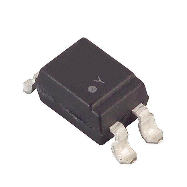
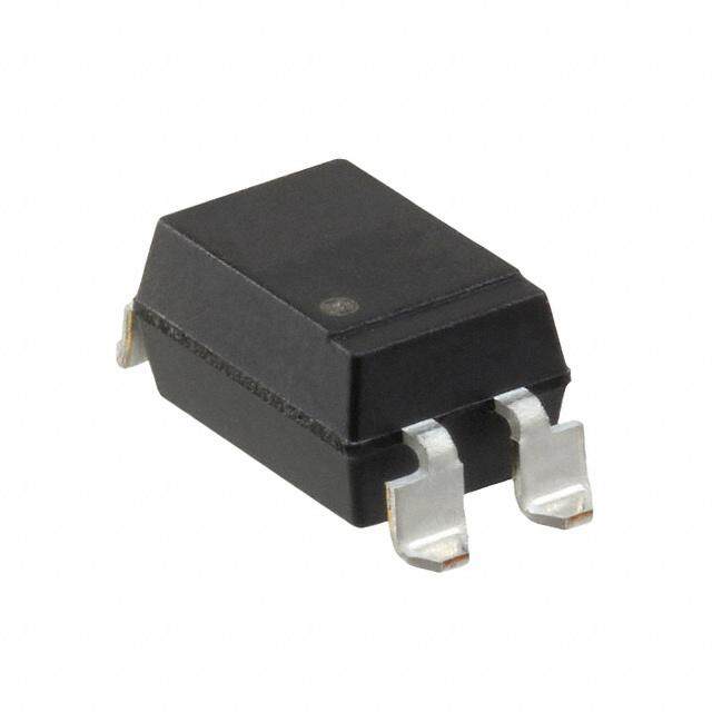
| 产品图片 |
|
| 产品型号 | 4N37S-TA1 |
| rohs | 无铅 / 符合限制有害物质指令(RoHS)规范要求 |
| 产品系列 | - |
| Vce饱和值(最大值) | 300mV |
| 上升/下降时间(典型值) | 3µs, 3µs |
| 供应商器件封装 | 6-SMD |
| 其它名称 | 160-1913-2 |
| 包装 | 带卷 (TR) |
| 安装类型 | 表面贴装 |
| 封装/外壳 | 6-SMD,鸥翼型 |
| 工作温度 | -55°C ~ 100°C |
| 打开/关闭时间(典型值) | - |
| 标准包装 | 1,000 |
| 电压-正向(Vf)(典型值) | 1.2V |
| 电压-输出(最大值) | 30V |
| 电压-隔离 | 1500Vrms |
| 电流-DC正向(If) | 60mA |
| 电流-输出/通道 | 100mA |
| 电流传输比(最大值) | - |
| 电流传输比(最小值) | 100% @ 10mA |
| 输入类型 | DC |
| 输出类型 | 有基极的晶体管 |
| 通道数 | 1 |


.jpg)


.jpg)


- 商务部:美国ITC正式对集成电路等产品启动337调查
- 曝三星4nm工艺存在良率问题 高通将骁龙8 Gen1或转产台积电
- 太阳诱电将投资9.5亿元在常州建新厂生产MLCC 预计2023年完工
- 英特尔发布欧洲新工厂建设计划 深化IDM 2.0 战略
- 台积电先进制程称霸业界 有大客户加持明年业绩稳了
- 达到5530亿美元!SIA预计今年全球半导体销售额将创下新高
- 英特尔拟将自动驾驶子公司Mobileye上市 估值或超500亿美元
- 三星加码芯片和SET,合并消费电子和移动部门,撤换高东真等 CEO
- 三星电子宣布重大人事变动 还合并消费电子和移动部门
- 海关总署:前11个月进口集成电路产品价值2.52万亿元 增长14.8%

PDF Datasheet 数据手册内容提取
Photocoupler Product Data Sheet 4N35/ 4N37 (M, S, S-TA1) Spec No. :DS-70-99-0012 Effective Date: 08/22/2017 Revision: E LITE-ON DCC RELEASE BNS-OD-FC001/A4 LITE-ON Technology Corp. / Optoelectronics No.90,Chien 1 Road, Chung Ho, New Taipei City 23585, Taiwan, R.O.C. Tel: 886-2-2222-6181 Fax: 886-2-2221-1948 / 886-2-2221-0660 http://www.liteon.com/opto
Photocoupler 4N3X series 1. DESCRIPTION 1.1 Features (cid:1) Current transfer ratio (CTR : MIN. 100% at I = 10mA, V = 10V, Ta=25oC) F CE (cid:1) High input-output isolation voltage 4N35 series : Viso = 3,550Vrms 4N37 series : Viso = 1,500Vrms (cid:1) Response time (tr : TYP. 3m s at Vcc = 10V, IC = 2mA, RL = 100W ) (cid:1) Dual-in-line package : 4N35, 4N37 (cid:1) Wide lead spacing package : 4N35M, 4N37M (cid:1) Surface mounting package : 4N35S, 4N37S (cid:1) Tape and reel packaging : 4N35S-TA, 4N37S-TA, 4N35S-TA1, 4N37S-TA1 (cid:1) Safety approval * UL approved (No. E113898) * CSA approved (No. CA91533-1) * FIMKO approved ( No. 193422-01) * VDE approved ( No. 40015248) * BSI approved (No. 9018-9) * CQC approved (No.CQC11001061921-2) (cid:1) Creepage distance > 8.0 mm ; Clearance > 8.0 mm (cid:1) The relevant models are the models Approved by VDE according to DIN EN 60747-5-5 Approved Model No.: 4N35-V / 4N37-V / 4N35M-V / 4N37M-V / 4N35S-V / 4N37S-V / 4N35STA-V / 4N37STA-V / 4N35STA1-V / 4N37STA1-V VDE approved No.: 40015248 (According to the specification DIN EN 60747-5-5) (cid:1) Operating isolation voltage VIORM : 420V (Peak) (cid:1) Transient voltage VTR : 6000V (Peak) (cid:1) Pollution : 2 (According to VDE 0110-1 : 1997-04) (cid:1) Clearances distance (Between input and output) : 7.0mm (MIN.) (cid:1) Creepage distance (Between input and output) : 7.0mm (MIN.) (cid:1) Isolation thickness between input and output : 0.4mm (MIN.) (cid:1) Safety limit values Current (Isi) : 400mA (Diode side) Power (Psi) : 700mW (Phototransistor side) Temperature(Tsi) : 175oC In order to keep safety electric isolation of photocoupler, please set the protective circuit to keep within safety limit values when the actual application equipment troubled. (cid:1) Indication of VDE approval prints " " on sleeve package. 1/15 Pa rt No . : 4N 3X serie s BNS-OD-FC002/A4 Rev.: D
Photocoupler 4N3X series (cid:1) RoHS Compliance All materials be used in device are followed EU RoHS directive (No.2002/95/EC). (cid:1) ESD pass HBM 8000V/MM2000V (cid:1) MSL class1 1.2 Applications (cid:1) Power Supply regulators (cid:1) Digital logic inputs (cid:1) Microprocessor inputs 2/15 Pa rt No . : 4N 3X serie s BNS-OD-FC002/A4 Rev.: D
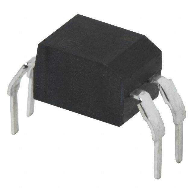
Photocoupler 4N3X series 2. PACKAGE DIMENSIONS 2.1 4N35 2.2 4N35M 2.3 4N35S Notes : 1. Year date code. 2. 2-digit work week. 3. Factory identification mark shall be marked (W: China-CZ, Y: Thailand X: China-TJ). 4. VDE option. Dimensions in millimeters(inches). 3/15 Pa rt No . : 4N 3X serie s BNS-OD-FC002/A4 Rev.: D
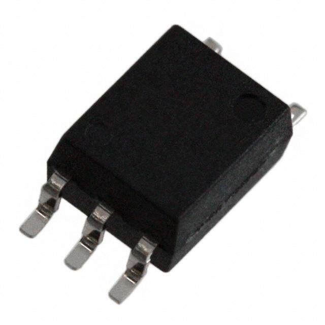
Photocoupler 4N3X series 2.4 4N37 2.5 4N37M 2.6 4N37S Notes : 1. Year date code. 2. 2-digit work week. 3. Factory identification mark shall be marked (W: China-CZ, Y: Thailand X: China-TJ). 4. VDE option. Dimensions in millimeters(inches). 4/15 Pa rt No . : 4N 3X serie s BNS-OD-FC002/A4 Rev.: D
Photocoupler 4N3X series 3. TAPING DIMENSIONS 3.1 4N35S-TA , 4N37S-TA : 3.2 4N35S-TA1 , 4N37S-TA1 : Description Symbol Dimension in mm (inch) Tape wide W 16±0.3 (0.63) Pitch of sprocket holes P 4±0.1 (0.15) 0 F 7.5±0.1 (0.295) Distance of compartment P 2±0.1 (0.079) 2 Distance of compartment to P 12±0.1 (0.472) compartment 1 3.3 Quantities Per Reel Package Type TA/TA1 Quantities (pcs) 1000 5/15 Pa rt No . : 4N 3X serie s BNS-OD-FC002/A4 Rev.: D
Photocoupler 4N3X series 4. RATING AND CHARACTERISTICS 4.1 Absolute Maximum Ratings at Ta=25°C Parameter Symbol Rating Unit Forward Current I 60 mA F Input Reverse Voltage V 6 V R Power Dissipation P 100 mW Collector - Emitter Voltage V 30 V CEO Emitter - Collector Voltage V 7 V ECO Output Collector - Base Voltage V 70 V CBO Collector Current I 100 mA C Collector Power Dissipation P 300 mW C Total Power Dissipation P 350 mW tot 4N35 series 3,550 V rms *1 Isolation Voltage V iso 4N37 series 1,500 V rms Operating Temperature Topr -55 ~ +100 °C Storage Temperature Tstg -55 ~ +150 °C *2 Soldering Temperature Tsol 260 °C *1. AC For 1 Minute, R.H. = 40 ~ 60% Isolation voltage shall be measured using the following method. (1) Short between anode and cathode on the primary side and between collector and emitter on the secondary side. (2) The isolation voltage tester with zero-cross circuit shall be used. (3) The waveform of applied voltage shall be a sine wave. *2. For 10 Seconds 6/15 Pa rt No . : 4N 3X serie s BNS-OD-FC002/A4 Rev.: D
Photocoupler 4N3X series 4.2 ELECTRICAL OPTICAL CHARACTERISTICS at Ta=25°C PARAMETER SYMBOL MIN. TYP. MAX. UNIT CONDITIONS Forward Voltage VF — 1.2 1.5 V IF=10mA INPUT Reverse Current IR — — 10 m A VR=4V Terminal Capacitance Ct — 50 — pF V=0, f=1KHz Collector Dark Ta=25(cid:176) C — — 50 nA VCE=10V, IF=0 ICEO Current Ta=100(cid:176) C — — 500 µA VCE=30V, IF=0 Collector-Emitter IC=0.1mA BVCEO 30 — — V OUTPUT Breakdown Voltage IF=0 Emitter-Collector Breakdown IE=10m A BVECO 7 — — V Voltage IF=0 Collector-Base IC=0.1mA BVCBO 70 — — V Breakdown Voltage IF=0 Collector Current IC 10 — — mA IF=10mA *Current Transfer Ratio CTR 100 — — % VCE=10V Collector-Emitter IF=50mA VCE(sat) — — 0.3 V S a tu r a t io n V o l ta g e IC=2mA TRANSFER DC500V Isolation Resistance Riso 5· 1010 1· 1011 — W CHARACTERISTICS 40 ~ 60% R.H. Floating Capacitance Cf — 1 2.5 pF V=0, f=1MHz Response Time (Rise) tr — 3 10 m s VCE=10V, IC=2mA Response Time (Fall) tf — 3 10 m s RL=100W I *CTR= C · 100% I F 7/15 Pa rt No . : 4N 3X serie s BNS-OD-FC002/A4 Rev.: D
Photocoupler 4N3X series 4.3 ISOLATION SPECIFICATION ACCORDING TO VDE Parameter Symbol Conditions Rating Unit Remark Class of environmental test - DIN IEC68 55/100/21 - Pollution - DIN VDE0110 2 - Maximum Operating V - 420 V IORM PEAK Isolation Voltage Partial Discharge Test Diagram 1 tp=60s, qc<5pC 630 VPEAK Refer to the Diagram Voltage (Between Input Vpr 1, 2 Diagram 2 tp=1s, qc<5pC 788 V and Output) PEAK Maximum Over-Voltage V t = 10s 6000 V INITIAL INI PEAK Safety Maximum Ratings 1) Case Temperature Tsi I = 0, Pc = 0 175 oC F Refer to the 2) Input Current Isi Pc=0 400 mA Figure 1, 3 3) Electric Power (Output or Total Psi - 700 mW Power Issipation) Ta=Tsi MIN.109 Isolation Resistance (Test Voltage Between RISO Ta=Topr(MAX.) MIN.1011 W Input and Output : DC500V) Ta=25 oC MIN.1012 Precautions in performing isolation test * Partial discharge test methods shall be the ones according to the specifications of DIN EN 60747-5-5 * Please don't carry out isolation test (Viso) over V ,This product deteriorates INITIAL isolation characteristics by partial discharge due to applying high voltage (ex. V ). And there is possibility that this product occurs partial discharge in INITIAL operating isolation voltage (V ) IORM 8/15 Pa rt No . : 4N 3X serie s BNS-OD-FC002/A4 Rev.: D
Photocoupler 4N3X series 4.4 PARTIAL DISCHARGE TEST METHOD Method (A) for type testing and random testing. V VINTIAL Vpr t1, t2 =1 to 10s t3, t4 =1s V IORM tp (Partial Discharge Measuring Time)=60s tb =62s tini =10s t t3 tp t4 t1 tini t2 tb Method (B) for routine testing. V V pr t3, t4 =0.1s tp (Partial Discharge Measuring Time)=1s tb =1.2s V IORM t t3 tp t4 tb The partial discharge level shall not exceed 5 pc during the partial discharge measuring time interval t under the test p conditions shown above. 9/15 Pa rt No . : 4N 3X serie s BNS-OD-FC002/A4 Rev.: D
Photocoupler 4N3X series 5. CHARACTERISTICS CURVES Fig.1 Forward Current vs. Ambient Fig.2 Collector Power Dissipation vs. Temperature Ambient Temperature 100 200 )W m )Am 80 (cnP 150 t I rr(uenF 60 issdiitpao 100 roFw radc 4200 tr r ceopoew 50 llo 0 C 0 -55 -25 0 25 50 75 100 125 -55 -25 0 25 50 75 100 125 Ambient temperature Ta ( oC) Ambient temperature Ta ( oC) Fig.3 Forward Current vs. Forward Fig.4 Current Transfer Ratio vs. Forward Voltage Current 500 50 V =10V o )% Ta=25 oC )A 200 o o (R 40 r rrt I (adcuenmF110520000 oo rfr rsTaneit aoTC 3200 roFw 5 rrt uen 10 R = 2 C 100k 1 0 0 0.5 1.0 1.5 2.0 2.5 3.0 0.10.2 0.51 2 5 10 20 50 100 Forward voltage V F (V) Forward current I F (mA) Fig.5 Collector Current vs. Fig.6 Relative Current Transfer Ratio Collector-emitter Voltage vs. Ambient Temperature 15 300 t In ()cAm 10 Ta=25 oC I F =3400mmAA Pc(MAX.) f rsneti r()ao% 200 IV F = =101m0VA e a llt rrrccoeouC 5 2100mmAA ti t trrrvcaeuen 100 5mA leR 0 0 0 5 10 15 -55 -25 0 25 50 75 100 Collector-emitter voltage VC E (V) Ambient temperature Ta ( oC) 10/15 Part No. : 4N3 X ser ies BNS-OD-FC002/A4 Rev.: D
Photocoupler 4N3X series Fig.7 Collector-emitter Saturation Voltage vs. Fig.8 Collector Dark Current vs. Ambient Temperature Ambient Temperature 0.3 10-6 ge IF=50mA 5 V =10V ilrt tvuaonoa 0.2 IC=2mA (t I)enACEO 1100---78955 itmtr tsea rrrkcdau 1100-1055 lltr-coeoet)()saV(EC 0.1 Cllt rcoeo 110-01255 CV 0 10-13 -55 -25 0 25 50 75 100 -55 -25 0 20 40 60 100 125 Ambient temperature Ta ( OC) Ambient temperature Ta ( OC) Fig.9 Response Time vs. Load Resistance Fig.10 Frequency Response 100 5 V =10V V =5V 50 Ic=2mA tf tr Ic=2mA Ta=25 OC 0 Ta=25 OC Ri t ( )ssseponeem 0 12 . 152500 tstd ltoagV i ()vegandAB - 1-05 R L=10k 1k 100 -15 0.2 0.1 -20 0.05 0.1 0.20.5 1 2 5 10 20 50 0.5 1 2 5 10 20 50100200 500 Load resistance RL(k ) Frequency f (kHz) Fig.11 Collector-emitter Saturation Test Circuit for Response Time Voltage vs. Forward Current Input 7 Vcc ltvoage 6 .05Am 1Am2Am3Am 5Am 7Am Ta=25 OC Input RD RL OutpuOtutput 10% ti aon 5 Ic= 90% trau 4 td ts s mitt re 3 Test Circuit for Frequency Respontrse tf lltr-coeoeCt)()saVV(EC 120 RD RVLcc Output 0 5 10 15 20 25 30 Forward current IF(mA) 11/15 Part No. : 4N3 X se ries BNS-OD-FC002/A4 Rev.: D
Photocoupler 4N3X series 6. TEMPERATURE PROFILE OF SOLDERING 6.1 IR Reflow soldering (JEDEC-STD-020C compliant) One time soldering reflow is recommended within the condition of temperature and time profile shown below. Do not solder more than three times. Profile item Conditions Preheat - Temperature Min (T ) 150˚C Smin - Temperature Max (T ) 200˚C Smax - Time (min to max) (ts) 90±30 sec Soldering zone - Temperature (T ) 217˚C L - Time (t ) 60 sec L Peak Temperature (T ) 260˚C P Ramp-up rate 3˚C / sec max. Ramp-down rate 3~6˚C / sec 20 sec Ramp-up TP260 C TL217 C ) C Tsmax200 C Ramp-down ( e r u at Tsmin 60 sec er 150 C tL (Soldering) p m e T 25 C Time (sec) 60 ~ 120 sec 35~70 sec ts (Preheat) 12/15 Part No. : 4N3 X ser ies BNS-OD-FC002/A4 Rev.: D
Photocoupler 4N3X series 6.2 Wave soldering (JEDEC22A111 compliant) One time soldering is recommended within the condition of temperature. Temperature: 260+0/-5˚C Time: 10 sec. Preheat temperature:25 to 140˚C Preheat time: 30 to 80 sec. 6.3 Hand soldering by soldering iron Allow single lead soldering in every single process. One time soldering is recommended. Temperature: 380+0/-5˚C Time: 3 sec max. 13/15 Part No. : 4N3 X ser ies BNS-OD-FC002/A4 Rev.: D
Photocoupler 4N3X series 7. RRECOMMENDED FOOT PRINT PATTERNS (MOUNT PAD) Unit: mm 14/15 Part No. : 4N3 X ser ies BNS-OD-FC002/A4 Rev.: D
Photocoupler 4N3X series 8. Naming rule 4N3X (1)-( 2) DEVICE PART NUMBER (1) No suffix = Dual-in-Line package M = Wide lead spacing package S = Surface mounting package (2) TAPING TYPE (TA,TA1 or none) 4N3X series have tape and reel solution. Please refer to orientation of taping on Page P5 Example : 4N35S-TA1 4N3X(1)( 2)-V DEVICE PART NUMBER (1) No suffix = Dual-in-Line package M = Wide lead spacing package S = Surface mounting package (2) TAPING TYPE (TA,TA1 or none) 4N3X series have tape and reel solution. Please refer to orientation of taping on Page P5 (3) VDE order option Example : 4N35STA1-V-G 9. Notes: (cid:1) LiteOn is continually improving the quality, reliability, function or design and LiteOn reserves the right to make changes without further notices. (cid:1) The products shown in this publication are designed for the general use in electronic applications such as office automation equipment, communications devices, audio/visual equipment, electrical application and instrumentation. (cid:1) For equipment/devices where high reliability or safety is required, such as space applications, nuclear power control equipment, medical equipment, etc, please contact our sales representatives. (cid:1) When requiring a device for any “specific” application, please contact our sales in advice. (cid:1) If there are any questions about the contents of this publication, please contact us at your convenience. (cid:1) The contents described herein are subject to change without prior notice. (cid:1) Immerge unit’s body in solder paste is not recommended. 15/15 Part No. : 4N3 X ser ies BNS-OD-FC002/A4 Rev.: D